EP1749330B1 - Antenna radiator structures - Google Patents
Antenna radiator structures Download PDFInfo
- Publication number
- EP1749330B1 EP1749330B1 EP05780139A EP05780139A EP1749330B1 EP 1749330 B1 EP1749330 B1 EP 1749330B1 EP 05780139 A EP05780139 A EP 05780139A EP 05780139 A EP05780139 A EP 05780139A EP 1749330 B1 EP1749330 B1 EP 1749330B1
- Authority
- EP
- European Patent Office
- Prior art keywords
- radiator
- array
- dielectric
- strip
- conductor pattern
- Prior art date
- Legal status (The legal status is an assumption and is not a legal conclusion. Google has not performed a legal analysis and makes no representation as to the accuracy of the status listed.)
- Expired - Lifetime
Links
Images





Classifications
-
- H—ELECTRICITY
- H01—ELECTRIC ELEMENTS
- H01Q—ANTENNAS, i.e. RADIO AERIALS
- H01Q13/00—Waveguide horns or mouths; Slot antennas; Leaky-waveguide antennas; Equivalent structures causing radiation along the transmission path of a guided wave
- H01Q13/08—Radiating ends of two-conductor microwave transmission lines, e.g. of coaxial lines, of microstrip lines
- H01Q13/085—Slot-line radiating ends
-
- H—ELECTRICITY
- H01—ELECTRIC ELEMENTS
- H01Q—ANTENNAS, i.e. RADIO AERIALS
- H01Q1/00—Details of, or arrangements associated with, antennas
- H01Q1/08—Means for collapsing antennas or parts thereof
- H01Q1/085—Flexible aerials; Whip aerials with a resilient base
-
- H—ELECTRICITY
- H01—ELECTRIC ELEMENTS
- H01Q—ANTENNAS, i.e. RADIO AERIALS
- H01Q1/00—Details of, or arrangements associated with, antennas
- H01Q1/08—Means for collapsing antennas or parts thereof
- H01Q1/085—Flexible aerials; Whip aerials with a resilient base
- H01Q1/087—Extensible roll- up aerials
-
- H—ELECTRICITY
- H01—ELECTRIC ELEMENTS
- H01Q—ANTENNAS, i.e. RADIO AERIALS
- H01Q1/00—Details of, or arrangements associated with, antennas
- H01Q1/36—Structural form of radiating elements, e.g. cone, spiral, umbrella; Particular materials used therewith
- H01Q1/38—Structural form of radiating elements, e.g. cone, spiral, umbrella; Particular materials used therewith formed by a conductive layer on an insulating support
Definitions
- Some active array apertures are under stringent weight and space constrains. For example, space based arrays need to be delivered into space, and so there a stringent weight and space limitations imposed by the lounge vehicle capabilities.
- Another example application involves stowing an array for battlefield deployment, e.g. when such an array is carried by a weight sensitive transport such as sole aperture.
- US 5,313,221 A discloses a self-deployable phased array radar antenna which comprises antenna blades as radiating elements. The antenna may be bent. This document discloses the preamble of claim 1.
- EP 197 29 64 A1 discloses a planar wide band antenna using coplanar wave guides.
- EP 0 477 951 A2 relates to a dielectric flair notch radiator with separate transmit and receive ports.
- a foldable radiator assembly includes a thin, flexible dielectric substrate structure having a radiator conductor pattern formed therein.
- the flexible substrate structure is flexible for movement between a folded position and a deployed position.
- An excitation circuit excites the radiator conductor pattern with RF energy.
- Strips of the radiator assemblies can be used to form an array aperture.
- FIG. 1 is an isometric view of an embodiment of a foldable antenna array in a deployed state.
- FIG. 2 is an exploded isometric view of a further exemplary embodiment of a foldable antenna array assembly.
- FIG. 3 is a schematic block diagram of a balun circuit.
- FIG. 4 is an exploded side view of an embodiment of a pop-up flare dipole radiator assembly.
- FIG. 5 is an isometric view of another embodiment of a pop-up flare dipole radiator assembly.
- FIG. 5A is a side view illustrating the transition from a coplanar strip transmission line to 2-wire transmission line employed in the flare dipole radiator assembly of FIG. 5 .
- FIG. 6 is an isometric view illustrating a mechanical layout of an embodiment of a pop-up flare dipole radiator structure.
- FIG. 6A is a side view of the embodiment of FIG. 6 , illustrating an exemplary 90 degree deployed position.
- FIGS. 7A-7D illustrate in successive isometric views the folded state of the radiator structure of FIG. 6 ( FIG. 7A ), intermediate states ( FIGS. 7B-7C ), and the deployed, operating position ( FIG. 7D ).
- FIG. 8 is a partially broken-away fragmentary isometric view of an embodiment of an antenna array, with the flexible radiating structures in fixed positions.
- FIG. 9 is an isometric view of a single fold TEM horn radiator array in a deployed state.
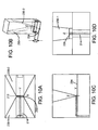
- FIG. 10A is a bottom view of a TEM radiator model.
- FIG. 10B is an isometric view of the TEM radiator model.
- FIGS. 10C is a front view of the TEM radiator model.
- FIG. 10D is a side view of the TEM radiator model.
- FIG. 11 is an isometric view of a two-dimensional antenna aperture formed by strips of foldable TEM horn radiators arrayed along the E-plane.
- FIG. 12 is an isometric view of a two-dimensional antenna aperture formed by multiple folds of a continuous sheet of flexible circuit material forming TEM horn radiators.
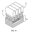
- FIG. 13 is an exploded view of an array of printed flexible TEM horns mounted on a planar active array panel assembly.
- FIGS. 14A-14C diagrammatically depict the array of FIG. 13 in respective folded, partially unfolded and fully deployed states.
- FIG. 15 is an isometric view of a foldable TEM horn array including a dielectric line arrangement to control radiator position.
- Embodiments of a thin lightweight wide band radiating element and array structure are described Exemplary applications for these embodiments include space based active array antennas.
- the radiator is foldable or rollable into a stored configuration for low volume storage within a rocket, for example, to increase the amount of antenna aperture that can be stored within a fixed volume e.g. in the rocket prior to launch.
- the radiator may be configured to pop-up by itself to the proper operating shape and configuration, or to be deployed by a dielectric line.
- the antenna can be fixed in position.
- a radiator structure 20 includes radiator elements 30 similar to the flared dipole radiator described in U.S. 5,428,364 , but with a coplanar strip transmission line (CPS) 40 comprising conductor strips 40-1 and 40-2 feeding the flared dipole section (including flared dipole elements 30-1 and 30-2) that incorporates a 90 degree H-plane bend 42, forming a CPS to microstrip transition 50.
- the 90 degree H-plane bend is realized using thin, e.g. less than 4 mils thick, flexible dielectric circuit material such as polyimide, liquid crystal polymer (LCP), polyester, or duroid to form the dielectric substrate 22.
- the flexible circuit board material is copper cladded with the shape of the flared dipole etched onto the copper, e.g., using conventional circuit fabrication processes.
- a flexible dielectric layer can optionally be formed on the flexible circuit board, e.g. to add stiffness or prevent shorting if needed for a particular application.
- FIGS. 2-5A illustrate an exemplary embodiment of an exemplary assembly 100.
- the radiator structure 20 is mounted onto a dielectric insulator layer 110 that is laid over the antenna aperture groundplane structure 120.
- the groundplane structure 120 comprises a top groundplane layer 122, e.g. fabricated of a copper layer on a top surface of a top dielectric layer 126A.
- a lower groundplane layer 124 is formed on a bottom surface of a dielectric layer 126B.
- An air strip line layer 127 is assembled between the groundplane layers 122, 124 by z-axis anisotropically conductive adhesive layers 125.
- the input of the coplanar strip transmission line section is orthogonally transitioned through the dielectric insulator layer 110 using plated through vias 90, 92 ( FIG. 5 ) in the form of a 2-wire transmission line 94, as illustrated in FIG. 5A , which has a similar E-field configuration to that of the CPS transmission line.
- the strips 40-1, 40-2 of the CPS line are connected to respective conductive vias 90, 92.
- An opening or clearout 122A in the top groundplane layer122 allows the 2-wire transmission line above the groundplane to continue through and connect to a corresponding 2-wire transmission line including stripline conductor trace 130 ( FIG. 4 ), which then transitions orthogonally to the "balance" arms of a balun circuit, described below.
- a balun circuit 160 is used to transform single ended or "unbalanced" transmission lines, typically used for many RF devices, to double ended or “balanced” transmission lines, as illustrated in FIG. 3 .
- unbalanced transmission lines include coaxial, microstrip, coplanar waveguide and stripline.
- balanced transmission lines include twin lead, 2-wire, coplanar strip and slotline.
- Balun circuits suitable for the purpose can be constructed by those skilled in the art. Examples of balun circuits are described, for example, in " Electromagnetic Simulation of Some Common Balun Structures," K.V.
- anisotropically conducting z-axis adhesive films 170, 172 FIG. 4
- Exemplary suitable commercially available anisotropically conducting z-axis adhesive films include the adhesive films marketed by 3M as part number 7373 and 9703.
- Catchpads 90A, 112A, 112B, 128A at the ends of the plated vias, e.g. vias 90, 112, 128 of each board layer make contact with the metal particles within the adhesive films to form a continuous DC/RF interconnect from the coplanar strip transmission line on the radiator to the stripline conductor 130 to the balun circuit 160 underneath the groundplane.
- the flared dipole radiator is a combination of the flared notch radiator and dipole radiator, resulting in a wider operating frequency for a short height.
- An RF signal is excited across the coplanar strip at the input port of the coplanar strip transmission line.
- the RF signal travels across the coplanar strip at the input port of the coplanar strip transmission line.
- the RF signal travels along the coplanar strip across an ever increasing gap until it radiates into free space at the end of the element.
- the upper frequency band is limited only by the balun design.
- the flare dipole overcomes the lower frequency limits by having its outer conductor edge shaped in the form of a dipole.
- the flared dipole functions as a conventional dipole which is much shorter than the conventional flared notch radiator operating for the same frequency band.
- the 90 degree H-plane bend can be incorporated into both the conventional dipole and flared notch radiators with little impact on RF performance.
- a feature of one exemplary embodiment of the radiator is its ability to fold down for low volume storage and later spring ("pop-up") to the proper operating position during deployment.
- the 90 degree H-plane bend is realized using thin 2 mil thick flexible circuit board material such as polyimide, LCP, polyester or duroid.
- the 90 degree H-plane bend in the radiator acts both as a spring and a hinge.
- Other angular deployed positions (i.e. other than 90 degree) of the radiator may also be used, depending on the requirements of a specific application.
- the radiator flexible material exerts an opposing force to return it to its original flat shape.
- slots 28 are formed in the flexible circuit board material at the hinge or fold line 25 to control the springback force, leaving areas 26 of the flexible circuit board material between the slots.
- Thin dielectric stiffener layers 48A, 48B are attached to the circuit board material, e.g. by nonconductive film adhesives, and provide stiffness and environmental protection.
- the stiffener layers are 4 mil fiberglass reinforced circuit board material.
- Gussets 24 are used to control the radiator H-plane bending to the desired 90 degree position while the thin stiffeners also control the radiator shape. The gussets in combination with the stiffener layers are thus used to shape the radiator to the proper operating configuration.
- FIGS. 5 and 6 The embodiment illustrated in FIGS. 5 and 6 is of a panel 10 fabricated from a thin sheet of flexible circuit board material, on which a plurality of flared dipole radiators 30 have been formed. Although in this example there are four radiators 30 shown, it will be appreciated that a panel with a greater number or a fewer number of radiators can be employed.
- a continuous sheet of flexible dielectric material can be used as a gusset to constrain the radiator strip, as depicted in FIG. 6
- thin strips 24A-24D ( FIG. 5 ) of flexible circuit material can also be used as gussets to position the radiator and thus eliminate potential excess material and weight. Further weight reduction can be achieved by using discrete pieces 110A, 110B, 110 C, 110D of insulating dielectric material as a spacer layer beneath the radiators, and allowing air space between the pieces, instead of a continuous dielectric layer.
- the feature of using thin flexible circuit board material, gussets and stiffeners for the flared dipole radiators can also be applied to the conventional discrete flared notch and dipole radiators.
- FIGS. 7A-7D illustrate the radiator panel 10 in several positions.
- the panel In FIG. 7A , the panel is in a folded position for storage.
- FIG. 7B the panel has started popping up, and is in a partially opened position.
- FIG. 7C shows the panel has moved further toward a fully deployed position.
- FIG. 7D shows the panel in a fully opened, deployed state, in an operating position.
- the stiffener and tie straps have controlled the movement of the radiator panel as it pops up from the folded position to the deployed, operating position.
- FIG. 8 illustrates in an isometric cutaway view an embodiment of a panel array 180, which comprises an array of flared dipole radiator structures 20, fabricated on flexible dielectric substrates.
- the radiator structures 20 are supported on a laminated RF feed assembly 184, similar to the planar antenna assembly comprising the dielectric insulator layer 110 and groundplane structure 120 of FIG. 4 , which includes balun circuits 186.
- the radiator structures 20 in this embodiment are in fixed position relative to the feed assembly 184.
- An aperture dielectric foam encapsulant 188 encapsulates the radiator strips at edges of and between strips of the radiator assemblies to support the radiators feed structures 20 in a fixed operating position. Orthogonal strips of dielectric material can also be used to form an "egg-crate" structure to support the radiator feed structures 20 in a fixed operating position.
- a dielectric radome structure 190 fits over the radiator structure.
- FIG. 9 A foldable antenna structure is shown in FIG. 9 .
- the radiator strip 200 is fabricated as a thin single layer flexible circuit 210 folded in the shape of a tear drop, as illustrated in the edge view of FIG. 9A .
- the conductor pattern 220 located on the inside of the fold, is flared such that its width is widest at the radiator output while its conductor width narrows at the input port where the radiator interfaces to the RF feed or balun circuit. Likewise, the separation between the two conductor halves is widest at the radiator output while the separation narrows at the input port.
- the folded arch 202 at the radiator output forms and sustains the radiator shape. Since the folded arch comprises thin flexible dielectric circuit material, it has little or no impact on the RF performance of the radiator and is considered relatively invisible at microwave frequencies.
- the combination of the physical tear drop shape by the flexible circuit board when folded along with the flared conductor shape thus results in the realization of a wide band TEM flared horn radiator.
- the exemplary radiator structure 200 as illustrated in FIG. 9 has five TEM flared horn radiators 230 formed by the conductor pattern 220, although it will be understood that a greater number or a fewer number of horn radiators can be implemented in a folded radiator structure.
- FIG. 9 further illustrates how a plurality of radiator strips 200 can be positioned in a side-by-side arrangement along the E-plane to provide an two dimensional aperture of TEM flared horn radiators. This is shown in further detail in FIG. 11 , showing three radiator strips 200' arranged along the E-plane, each having three horns 230 defined therein to provide a 3x3 array. Each horn radiator has an RF feed port 232' at the radiator base 234'.
- the radiator assembly is fabricated using thin (e.g. ⁇ 4 mils thick) flexible circuit board material such as polyimide, LCP, polyester, or duroid.
- the flexible circuit board material is copper clad with the shape of the flared dipole etched onto the copper, e.g. using conventional circuit fabrication processes.
- FIGS. 10A-10D One exemplary technique for feeding microwave energy into the radiator is illustrated in FIGS. 10A-10D .
- a coaxial probe 212 excites a voltage across the two halves 230-1, 230-2 of the radiator at its input port 232.
- the coaxial outer conductor 214 is electrically connected to one half, e.g. 230-1 using either conductive epoxy or solder while the center pin penetrates through a clearance hole 236 in the one half 230-1 to contact the opposite half 230-2 of the radiator using either conductive epoxy or solder.
- the back of the radiator is open circuited at its base to force the microwave signal to flow between the flare conductor patterns to the radiator output. Shielded strip line can also be used in place of the coaxial cable to excite a voltage potential across the two halves of the radiator.
- a groundplane 238 is positioned 1/4 8 below the base 234 of the radiator 230.
- Alternative techniques for driving the radiator include a balun circuit as discussed above, e.g. with respect
- a single tear drop fold of a large flexible circuit board can form several horn radiators along the H-plane. Note that this differs from conventional printed flared notch radiator strips which are formed along the E-plane. As noted above, a two dimensional array antenna aperture can be formed by arranging several radiator strips together along the E-plane as shown in FIGS. 9 and 11 . This differs from the conventional printed flared notch radiator strips in which a two dimensional array antenna can be formed by arranging several radiator strips together along the H-plane.
- FIG. 12 illustrates a TEM horn radiator structure 250 forming a 3x3 array of horn radiators.
- the array is fabricated from a continuous sheet 260 of flexible circuit material, in contrast to each radiator strip being fabricated from a separate sheet of material as with the embodiment of FIG. 10 .
- the sheet 260 has formed on an interior surface the conductor pattern 220" which defines the TEM horn radiators. The sheet is folded in such a way as to provide the folded dielectric arches 202" and the RF feed points 232" adjacent the radiator base 234".
- a similar spacing between strip portions along the E-plane is provided by the folding arrangement.
- the base 234" formed by the continuous sequential bending of horn radiator strip forms a flat/conformal surface that can mounted onto a multilayer print circuit board panel assembly containing T/R modules, circulators, storage capacitors and microwave, digital and power manifolds.
- the combined aperture and panel assembly thus realizes a 2-D active array antenna.
- An exemplary embodiment of active array antenna 300 is shown in FIG. 13 , in which an array 310 of printed circuit flexible TEM horn radiators fabricated from a continuous sheet of flexible circuit material is mounted on a multilayer printed circuit board assembly 400, which functions as an RF feed, a digital and power manifold circuit. Circulators are embedded within the printed circuit assembly, and T/R modules and storage capacitors (not shown) can be mounted on the back of the assembly 400.
- this exemplary radiator is constructed as a folded assembly, the radiator generates an E-plane polarization perpendicular to the plane of the base assembly 400.
- FIGS. 14A-14C Using thin flexible circuit material to form the radiator aperture allows the aperture to bend and flatten for low volume storage prior to deployment as illustrated in FIGS. 14A-14C , e.g. for a payload in a rocket.
- FIG. 14A shows the aperture 310 in a compressed, folded condition for storage.
- FIG. 14B shows the radiators of the aperture 310 bent to one side
- FIG. 14C shows the radiator of the aperture in a fully deployed, open state wherein the radiators are essentially perpendicular to the plane of the base.
- One method of controlling the radiator shape and position during the fold down and deployment is to attach fibers to the flexible circuits to push and pull the thin walls of the radiator as illustrated in FIG. 1 15 .
- fibers or lines 410 are bonded to the top of the arch of the radiator strips, and are fabricated of a dielectric material.
- the fibers 410 can be pushed/pulled to move the TEM horns from the array aperture edge, and thereby control the radiator position.
- Other fibers or lines 412 can be bonded to the top of the arch and to the radiator base to control the radiator shape once deployed.
Landscapes
- Variable-Direction Aerials And Aerial Arrays (AREA)
- Details Of Aerials (AREA)
- Waveguide Aerials (AREA)
- Medicines Containing Material From Animals Or Micro-Organisms (AREA)
- Amplifiers (AREA)
Description
- Some active array apertures are under stringent weight and space constrains. For example, space based arrays need to be delivered into space, and so there a stringent weight and space limitations imposed by the lounge vehicle capabilities. Another example application involves stowing an array for battlefield deployment, e.g. when such an array is carried by a weight sensitive transport such as sole aperture.
-
US 5,313,221 A discloses a self-deployable phased array radar antenna which comprises antenna blades as radiating elements. The antenna may be bent. This document discloses the preamble ofclaim 1. -
DE 197 29 64 A1 discloses a planar wide band antenna using coplanar wave guides.EP 0 477 951 A2 relates to a dielectric flair notch radiator with separate transmit and receive ports. - There is a need for an array aperture that is relatively light weight. It would be an advantage to provide an array aperture which can be stored in a relatively small space.
- A foldable radiator assembly includes a thin, flexible dielectric substrate structure having a radiator conductor pattern formed therein. The flexible substrate structure is flexible for movement between a folded position and a deployed position. An excitation circuit excites the radiator conductor pattern with RF energy.
- Strips of the radiator assemblies can be used to form an array aperture.
- Features and advantages of the disclosure will readily be appreciated by persons skilled in the art from the following detailed description when read in conjunction with the drawing wherein:
-
FIG. 1 is an isometric view of an embodiment of a foldable antenna array in a deployed state. -
FIG. 2 is an exploded isometric view of a further exemplary embodiment of a foldable antenna array assembly. -
FIG. 3 is a schematic block diagram of a balun circuit. -
FIG. 4 is an exploded side view of an embodiment of a pop-up flare dipole radiator assembly. -
FIG. 5 is an isometric view of another embodiment of a pop-up flare dipole radiator assembly. -
FIG. 5A is a side view illustrating the transition from a coplanar strip transmission line to 2-wire transmission line employed in the flare dipole radiator assembly ofFIG. 5 . -
FIG. 6 is an isometric view illustrating a mechanical layout of an embodiment of a pop-up flare dipole radiator structure.FIG. 6A is a side view of the embodiment ofFIG. 6 , illustrating an exemplary 90 degree deployed position. -
FIGS. 7A-7D illustrate in successive isometric views the folded state of the radiator structure ofFIG. 6 (FIG. 7A ), intermediate states (FIGS. 7B-7C ), and the deployed, operating position (FIG. 7D ). -
FIG. 8 is a partially broken-away fragmentary isometric view of an embodiment of an antenna array, with the flexible radiating structures in fixed positions. -
FIG. 9 is an isometric view of a single fold TEM horn radiator array in a deployed state. -
FIG. 10A is a bottom view of a TEM radiator model.FIG. 10B is an isometric view of the TEM radiator model.FIGS. 10C is a front view of the TEM radiator model.FIG. 10D is a side view of the TEM radiator model. -
FIG. 11 is an isometric view of a two-dimensional antenna aperture formed by strips of foldable TEM horn radiators arrayed along the E-plane. -
FIG. 12 is an isometric view of a two-dimensional antenna aperture formed by multiple folds of a continuous sheet of flexible circuit material forming TEM horn radiators. -
FIG. 13 is an exploded view of an array of printed flexible TEM horns mounted on a planar active array panel assembly. -
FIGS. 14A-14C diagrammatically depict the array ofFIG. 13 in respective folded, partially unfolded and fully deployed states. -
FIG. 15 is an isometric view of a foldable TEM horn array including a dielectric line arrangement to control radiator position. - In the following detailed description and in the several figures of the drawing, like elements are identified with like reference numerals.
- Embodiments of a thin lightweight wide band radiating element and array structure are described Exemplary applications for these embodiments include space based active array antennas. The radiator is foldable or rollable into a stored configuration for low volume storage within a rocket, for example, to increase the amount of antenna aperture that can be stored within a fixed volume e.g. in the rocket prior to launch. When the antenna is unfolded or unrolled during deployment, the radiator may be configured to pop-up by itself to the proper operating shape and configuration, or to be deployed by a dielectric line. In other embodiments, the antenna can be fixed in position.
- In an exemplary embodiment illustrated in
FIG. 1 , aradiator structure 20 includesradiator elements 30 similar to the flared dipole radiator described inU.S. 5,428,364 , but with a coplanar strip transmission line (CPS) 40 comprising conductor strips 40-1 and 40-2 feeding the flared dipole section (including flared dipole elements 30-1 and 30-2) that incorporates a 90 degree H-plane bend 42, forming a CPS tomicrostrip transition 50. In an exemplary embodiment, the 90 degree H-plane bend is realized using thin, e.g. less than 4 mils thick, flexible dielectric circuit material such as polyimide, liquid crystal polymer (LCP), polyester, or duroid to form thedielectric substrate 22. The flexible circuit board material is copper cladded with the shape of the flared dipole etched onto the copper, e.g., using conventional circuit fabrication processes. A flexible dielectric layer can optionally be formed on the flexible circuit board, e.g. to add stiffness or prevent shorting if needed for a particular application. - Incorporating the 90 degree H-
plane bend 42 into the CPStransmission line portion 42 of theradiator 20 allows the radiator to be easily installed into a planar multilayer active array panel antenna assembly.FIGS. 2-5A illustrate an exemplary embodiment of anexemplary assembly 100. Theradiator structure 20 is mounted onto adielectric insulator layer 110 that is laid over the antennaaperture groundplane structure 120. Thegroundplane structure 120 comprises atop groundplane layer 122, e.g. fabricated of a copper layer on a top surface of a topdielectric layer 126A. Alower groundplane layer 124 is formed on a bottom surface of adielectric layer 126B. An airstrip line layer 127 is assembled between the groundplane layers 122, 124 by z-axis anisotropically conductive adhesive layers 125. - In this exemplary embodiment, the input of the coplanar strip transmission line section is orthogonally transitioned through the
dielectric insulator layer 110 using plated throughvias 90, 92 (FIG. 5 ) in the form of a 2-wire transmission line 94, as illustrated inFIG. 5A , which has a similar E-field configuration to that of the CPS transmission line. Thus, the strips 40-1, 40-2 of the CPS line are connected to respectiveconductive vias clearout 122A in the top groundplane layer122 allows the 2-wire transmission line above the groundplane to continue through and connect to a corresponding 2-wire transmission line including stripline conductor trace 130 (FIG. 4 ), which then transitions orthogonally to the "balance" arms of a balun circuit, described below. - A
balun circuit 160 is used to transform single ended or "unbalanced" transmission lines, typically used for many RF devices, to double ended or "balanced" transmission lines, as illustrated inFIG. 3 . Examples of unbalanced transmission lines include coaxial, microstrip, coplanar waveguide and stripline. Examples of balanced transmission lines include twin lead, 2-wire, coplanar strip and slotline. Balun circuits suitable for the purpose can be constructed by those skilled in the art. Examples of balun circuits are described, for example, in "Electromagnetic Simulation of Some Common Balun Structures," K.V. Puglia, IEEE Microwave Magazine, Application Notes, pages 56-61, September 2002; and "Review of Printed Marchand and Double Y Baluns: Characteristics and Application," Velimir Trifunovic and Branka Jokanovic, IEEE Transactions on Microwave Theory and Techniques, Vol. 42, No. 8, August 1994, pages 1454-1462. - Physical and microwave interconnect attachment of the
radiator 20 to the planar antenna assembly comprising thedielectric insulator layer 110 andgroundplane structure 120 is achieved using anisotropically conducting z-axisadhesive films 170, 172 (FIG. 4 ). Exemplary suitable commercially available anisotropically conducting z-axis adhesive films include the adhesive films marketed by 3M as part number 7373 and 9703.Catchpads stripline conductor 130 to thebalun circuit 160 underneath the groundplane. - The flared dipole radiator is a combination of the flared notch radiator and dipole radiator, resulting in a wider operating frequency for a short height. An RF signal is excited across the coplanar strip at the input port of the coplanar strip transmission line. The RF signal travels across the coplanar strip at the input port of the coplanar strip transmission line. The RF signal travels along the coplanar strip across an ever increasing gap until it radiates into free space at the end of the element. The upper frequency band is limited only by the balun design. The flare dipole overcomes the lower frequency limits by having its outer conductor edge shaped in the form of a dipole. At the low frequency band edge, the flared dipole functions as a conventional dipole which is much shorter than the conventional flared notch radiator operating for the same frequency band. The 90 degree H-plane bend can be incorporated into both the conventional dipole and flared notch radiators with little impact on RF performance.
- A feature of one exemplary embodiment of the radiator is its ability to fold down for low volume storage and later spring ("pop-up") to the proper operating position during deployment. In an exemplary embodiment illustrated in
FIGS. 6 and 6A , for example, the 90 degree H-plane bend is realized using thin 2 mil thick flexible circuit board material such as polyimide, LCP, polyester or duroid. The 90 degree H-plane bend in the radiator acts both as a spring and a hinge. Other angular deployed positions (i.e. other than 90 degree) of the radiator may also be used, depending on the requirements of a specific application. When folded at the H-plane bend, the radiator flexible material exerts an opposing force to return it to its original flat shape. In an exemplary embodiment,slots 28 are formed in the flexible circuit board material at the hinge or foldline 25 to control the springback force, leavingareas 26 of the flexible circuit board material between the slots. Thin dielectric stiffener layers 48A, 48B are attached to the circuit board material, e.g. by nonconductive film adhesives, and provide stiffness and environmental protection. In an exemplary embodiment, the stiffener layers are 4 mil fiberglass reinforced circuit board material.Gussets 24 are used to control the radiator H-plane bending to the desired 90 degree position while the thin stiffeners also control the radiator shape. The gussets in combination with the stiffener layers are thus used to shape the radiator to the proper operating configuration. - The embodiment illustrated in
FIGS. 5 and6 is of apanel 10 fabricated from a thin sheet of flexible circuit board material, on which a plurality of flareddipole radiators 30 have been formed. Although in this example there are fourradiators 30 shown, it will be appreciated that a panel with a greater number or a fewer number of radiators can be employed. - While a continuous sheet of flexible dielectric material can be used as a gusset to constrain the radiator strip, as depicted in
FIG. 6 ,thin strips 24A-24D (FIG. 5 ) of flexible circuit material can also be used as gussets to position the radiator and thus eliminate potential excess material and weight. Further weight reduction can be achieved by usingdiscrete pieces -
FIGS. 7A-7D illustrate theradiator panel 10 in several positions. InFIG. 7A , the panel is in a folded position for storage. InFIG. 7B , the panel has started popping up, and is in a partially opened position.FIG. 7C shows the panel has moved further toward a fully deployed position.FIG. 7D shows the panel in a fully opened, deployed state, in an operating position. The stiffener and tie straps have controlled the movement of the radiator panel as it pops up from the folded position to the deployed, operating position. -
FIG. 8 illustrates in an isometric cutaway view an embodiment of apanel array 180, which comprises an array of flareddipole radiator structures 20, fabricated on flexible dielectric substrates. Theradiator structures 20 are supported on a laminatedRF feed assembly 184, similar to the planar antenna assembly comprising thedielectric insulator layer 110 andgroundplane structure 120 ofFIG. 4 , which includesbalun circuits 186. Instead of folding, theradiator structures 20 in this embodiment are in fixed position relative to thefeed assembly 184. An aperturedielectric foam encapsulant 188 encapsulates the radiator strips at edges of and between strips of the radiator assemblies to support the radiators feedstructures 20 in a fixed operating position. Orthogonal strips of dielectric material can also be used to form an "egg-crate" structure to support theradiator feed structures 20 in a fixed operating position. Adielectric radome structure 190 fits over the radiator structure. - A foldable antenna structure is shown in
FIG. 9 . Theradiator strip 200 is fabricated as a thin single layerflexible circuit 210 folded in the shape of a tear drop, as illustrated in the edge view ofFIG. 9A . Theconductor pattern 220, located on the inside of the fold, is flared such that its width is widest at the radiator output while its conductor width narrows at the input port where the radiator interfaces to the RF feed or balun circuit. Likewise, the separation between the two conductor halves is widest at the radiator output while the separation narrows at the input port. The foldedarch 202 at the radiator output forms and sustains the radiator shape. Since the folded arch comprises thin flexible dielectric circuit material, it has little or no impact on the RF performance of the radiator and is considered relatively invisible at microwave frequencies. The combination of the physical tear drop shape by the flexible circuit board when folded along with the flared conductor shape thus results in the realization of a wide band TEM flared horn radiator. Theexemplary radiator structure 200 as illustrated inFIG. 9 has five TEM flaredhorn radiators 230 formed by theconductor pattern 220, although it will be understood that a greater number or a fewer number of horn radiators can be implemented in a folded radiator structure. -
FIG. 9 further illustrates how a plurality of radiator strips 200 can be positioned in a side-by-side arrangement along the E-plane to provide an two dimensional aperture of TEM flared horn radiators. This is shown in further detail inFIG. 11 , showing three radiator strips 200' arranged along the E-plane, each having threehorns 230 defined therein to provide a 3x3 array. Each horn radiator has an RF feed port 232' at the radiator base 234'. - In an exemplary embodiment, the radiator assembly is fabricated using thin (e.g. < 4 mils thick) flexible circuit board material such as polyimide, LCP, polyester, or duroid. The flexible circuit board material is copper clad with the shape of the flared dipole etched onto the copper, e.g. using conventional circuit fabrication processes.
- One exemplary technique for feeding microwave energy into the radiator is illustrated in
FIGS. 10A-10D . Acoaxial probe 212 excites a voltage across the two halves 230-1, 230-2 of the radiator at itsinput port 232. The coaxialouter conductor 214 is electrically connected to one half, e.g. 230-1 using either conductive epoxy or solder while the center pin penetrates through aclearance hole 236 in the one half 230-1 to contact the opposite half 230-2 of the radiator using either conductive epoxy or solder. The back of the radiator is open circuited at its base to force the microwave signal to flow between the flare conductor patterns to the radiator output. Shielded strip line can also be used in place of the coaxial cable to excite a voltage potential across the two halves of the radiator. Agroundplane 238 is positioned 1/4 8 below thebase 234 of theradiator 230. Alternative techniques for driving the radiator include a balun circuit as discussed above, e.g. with respect toFIGS. 3 and 4 . - As shown in
FIGS. 9 and11 , a single tear drop fold of a large flexible circuit board can form several horn radiators along the H-plane. Note that this differs from conventional printed flared notch radiator strips which are formed along the E-plane.
As noted above, a two dimensional array antenna aperture can be formed by arranging several radiator strips together along the E-plane as shown inFIGS. 9 and11 . This differs from the conventional printed flared notch radiator strips in which a two dimensional array antenna can be formed by arranging several radiator strips together along the H-plane. - If the sheet of flexible circuit board material is large enough, then a two dimensional array antenna aperture can be formed by incorporating" several tear drop folds to realize several radiator strips along the E-plane on a single sheet.
FIG. 12 illustrates a TEMhorn radiator structure 250 forming a 3x3 array of horn radiators. The array is fabricated from acontinuous sheet 260 of flexible circuit material, in contrast to each radiator strip being fabricated from a separate sheet of material as with the embodiment ofFIG. 10 . Thesheet 260 has formed on an interior surface theconductor pattern 220" which defines the TEM horn radiators. The sheet is folded in such a way as to provide the foldeddielectric arches 202" and the RF feed points 232" adjacent theradiator base 234". A similar spacing between strip portions along the E-plane is provided by the folding arrangement. The base 234" formed by the continuous sequential bending of horn radiator strip forms a flat/conformal surface that can mounted onto a multilayer print circuit board panel assembly containing T/R modules, circulators, storage capacitors and microwave, digital and power manifolds. The combined aperture and panel assembly thus realizes a 2-D active array antenna. An exemplary embodiment ofactive array antenna 300 is shown inFIG. 13 , in which anarray 310 of printed circuit flexible TEM horn radiators fabricated from a continuous sheet of flexible circuit material is mounted on a multilayer printedcircuit board assembly 400, which functions as an RF feed, a digital and power manifold circuit. Circulators are embedded within the printed circuit assembly, and T/R modules and storage capacitors (not shown) can be mounted on the back of theassembly 400. - Because this exemplary radiator is constructed as a folded assembly, the radiator generates an E-plane polarization perpendicular to the plane of the
base assembly 400. - Using thin flexible circuit material to form the radiator aperture allows the aperture to bend and flatten for low volume storage prior to deployment as illustrated in
FIGS. 14A-14C , e.g. for a payload in a rocket.FIG. 14A shows theaperture 310 in a compressed, folded condition for storage.FIG. 14B shows the radiators of theaperture 310 bent to one side, andFIG. 14C shows the radiator of the aperture in a fully deployed, open state wherein the radiators are essentially perpendicular to the plane of the base. One method of controlling the radiator shape and position during the fold down and deployment is to attach fibers to the flexible circuits to push and pull the thin walls of the radiator as illustrated inFIG. 1 15 . Here, fibers orlines 410 are bonded to the top of the arch of the radiator strips, and are fabricated of a dielectric material. Thefibers 410 can be pushed/pulled to move the TEM horns from the array aperture edge, and thereby control the radiator position. Other fibers orlines 412 can be bonded to the top of the arch and to the radiator base to control the radiator shape once deployed. - Although the foregoing has been a description and illustration of specific embodiments of the invention, various modifications and changes thereto can be made by persons skilled in the art without departing from the scope of the invention as defined by the following claims.
Claims (13)
- A foldable, pop-up radiator assembly (22, 210), comprising:a thin dielectric substrate structure (20) having a radiator conductor pattern (30, 220) formed therein, andan excitation circuit (40) for exciting the radiator conductor pattern with RF energy, whereinthe substrate structure (20) is flexible for movement between a folded position and a deployed position, wherein the substrate structure has a base portion mounted to a base structure, a flexing portion which is movable with respect to the base portion, and a hinge area (25) between said base portion and said flexing portion, said radiator conductor pattern being carried by the flexing portion,
characterized in that the radiator conductor pattern (30, 220) comprises a coplanar strip transmission line (40) which passes through said hinge area (25),
anda dielectric gusset structure (24) is connected between a distal portion of said flexing portion and said base portion to set the deployed position of the flexing portion. - A radiator assembly according to Claim 1, wherein the radiator conductor pattern is a flared dipole radiator pattern (30).
- A radiator assembly according to Claim 1, wherein the radiator conductor pattern is a TEM horn radiator pattern (230).
- A radiator assembly according to Claim 1, wherein the excitation circuit comprises a two-wire transmission structure (94) which is transverse to the base portion and which connects to respective conductors of the coplanar strip transmission line to form a vertical transition.
- A radiator assembly according to Claim 4, further comprising a balun circuit (160) coupled to the two-wire transition by a transmission structure (130) transverse to the two-wire transition.
- An array aperture comprising a strip of radiator assemblies (20, 200) as recited in Claim 1 and fabricated on a common unitary flexible substrate structure (260).
- An array aperture according to Claim 6, wherein the strip of radiator assemblies is oriented along an array H-plane.
- An array aperture according to Claim 7, further comprising a plurality of strips of the radiator assemblies, each strip oriented in parallel to the array H-plane and spaced along an array E-plane.
- An array aperture according to Claim 6, wherein the radiator conductor pattern is a TEM horn radiator pattern (230).
- An array aperture according to Claim 9, further comprising a plurality of strips of the radiator assemblies (20; 200), each strip oriented in parallel to and spaced relative to other strips.
- A radiator assembly according to Claim 1, wherein the dielectric gusset structure comprises a dielectric strip (24A).
- A radiator assembly according to Claim 1, wherein a flexing portion joins a base portion along, a hinge area (25) of the substrate assembly, and wherein a plurality of spaced slots (28) are formed through the dielectric substrate assembly along the joint area to control a springback force.
- A radiator assembly according to Claim 1, further comprising a dielectric line (410) attached to a flexing portion of the substrate structure for applying a deploying force to move the flexing portion to the deployed position.
Applications Claiming Priority (2)
| Application Number | Priority Date | Filing Date | Title |
|---|---|---|---|
| US10/856,443 US7057563B2 (en) | 2004-05-28 | 2004-05-28 | Radiator structures |
| PCT/US2005/012063 WO2006001873A1 (en) | 2004-05-28 | 2005-04-08 | Antenna radiator structures |
Publications (2)
| Publication Number | Publication Date |
|---|---|
| EP1749330A1 EP1749330A1 (en) | 2007-02-07 |
| EP1749330B1 true EP1749330B1 (en) | 2010-05-12 |
Family
ID=35197894
Family Applications (1)
| Application Number | Title | Priority Date | Filing Date |
|---|---|---|---|
| EP05780139A Expired - Lifetime EP1749330B1 (en) | 2004-05-28 | 2005-04-08 | Antenna radiator structures |
Country Status (6)
| Country | Link |
|---|---|
| US (1) | US7057563B2 (en) |
| EP (1) | EP1749330B1 (en) |
| JP (1) | JP4787248B2 (en) |
| DE (1) | DE602005021215D1 (en) |
| NO (1) | NO337507B1 (en) |
| WO (1) | WO2006001873A1 (en) |
Families Citing this family (45)
| Publication number | Priority date | Publication date | Assignee | Title |
|---|---|---|---|---|
| ATE396516T1 (en) * | 2003-07-25 | 2008-06-15 | Stichting Astron | DOUBLE POLARIZED ANTENNA ARRANGEMENT AND PROCESS FOR PRODUCTION THEREOF |
| JP2006086973A (en) * | 2004-09-17 | 2006-03-30 | Fujitsu Component Ltd | Antenna device |
| US7525498B2 (en) * | 2006-10-11 | 2009-04-28 | Raytheon Company | Antenna array |
| US8026863B2 (en) | 2006-10-11 | 2011-09-27 | Raytheon Company | Transmit/receive module communication and control architechture for active array |
| US8059049B2 (en) * | 2006-10-11 | 2011-11-15 | Raytheon Company | Dual band active array antenna |
| US7301500B1 (en) * | 2007-01-25 | 2007-11-27 | Cushcraft Corporation | Offset quasi-twin lead antenna |
| US7631414B2 (en) * | 2007-08-13 | 2009-12-15 | Raytheon Company | Methods for producing large flat panel and conformal active array antennas |
| JP5334242B2 (en) * | 2008-09-05 | 2013-11-06 | 大学共同利用機関法人自然科学研究機構 | Receive imaging antenna array |
| US8009114B2 (en) * | 2009-03-16 | 2011-08-30 | Raytheon Company | Flexible transmit/receive antenna pair using a switchable 0°/180° phase shifter |
| DE102009019557A1 (en) * | 2009-04-30 | 2010-11-11 | Kathrein-Werke Kg | A method of operating a phased array antenna and a phase shifter assembly and associated phased array antenna |
| JP5488593B2 (en) * | 2009-05-14 | 2014-05-14 | 株式会社村田製作所 | Circuit board and circuit module |
| US20110024160A1 (en) * | 2009-07-31 | 2011-02-03 | Clifton Quan | Multi-layer microwave corrugated printed circuit board and method |
| US8325102B2 (en) * | 2009-10-27 | 2012-12-04 | Raytheon Company | Single sheet phased array |
| US8127432B2 (en) | 2009-11-17 | 2012-03-06 | Raytheon Company | Process for fabricating an origami formed antenna radiating structure |
| US8362856B2 (en) * | 2009-11-17 | 2013-01-29 | Raytheon Company | RF transition with 3-dimensional molded RF structure |
| US9072164B2 (en) * | 2009-11-17 | 2015-06-30 | Raytheon Company | Process for fabricating a three dimensional molded feed structure |
| US8043464B2 (en) * | 2009-11-17 | 2011-10-25 | Raytheon Company | Systems and methods for assembling lightweight RF antenna structures |
| US8547280B2 (en) | 2010-07-14 | 2013-10-01 | Raytheon Company | Systems and methods for exciting long slot radiators of an RF antenna |
| US8654031B2 (en) * | 2010-09-28 | 2014-02-18 | Raytheon Company | Plug-in antenna |
| US8665600B2 (en) | 2010-11-29 | 2014-03-04 | Ratheon Company | Single sided feed circuit providing dual polarization |
| EP2602865B1 (en) * | 2011-12-05 | 2014-10-08 | Nxp B.V. | Multi-band antenna |
| US8847840B1 (en) | 2012-02-28 | 2014-09-30 | General Atomics | Pseudo-conductor antennas |
| US8773312B1 (en) * | 2012-02-29 | 2014-07-08 | General Atomics | Magnetic pseudo-conductor conformal antennas |
| US9190720B2 (en) * | 2012-03-23 | 2015-11-17 | Apple Inc. | Flexible printed circuit structures |
| US9685707B2 (en) * | 2012-05-30 | 2017-06-20 | Raytheon Company | Active electronically scanned array antenna |
| JP2014140136A (en) * | 2013-01-21 | 2014-07-31 | Nitto Denko Corp | Antenna module and method for manufacturing the same |
| US9225058B2 (en) * | 2013-03-15 | 2015-12-29 | Blackberry Limited | Flex PCB folded antenna |
| US9402303B2 (en) * | 2013-06-03 | 2016-07-26 | Apple Inc. | Flexible printed circuit cables with slits |
| US9876283B2 (en) | 2014-06-19 | 2018-01-23 | Raytheon Company | Active electronically scanned array antenna |
| JPWO2016031078A1 (en) * | 2014-08-26 | 2017-04-27 | イスイックス・ワールド株式会社 | Near-field director |
| US9979097B2 (en) * | 2016-03-16 | 2018-05-22 | Raytheon Company | Expanding lattice notch array antenna and method of fabrication |
| JP2019016926A (en) * | 2017-07-07 | 2019-01-31 | 株式会社フジクラ | Antenna device |
| US10826193B2 (en) | 2017-07-28 | 2020-11-03 | Samsung Electro-Mechanics Co., Ltd. | Antenna module including a flexible substrate |
| US10826186B2 (en) | 2017-08-28 | 2020-11-03 | Raytheon Company | Surface mounted notch radiator with folded balun |
| WO2019182492A1 (en) * | 2018-03-21 | 2019-09-26 | Telefonaktiebolaget Lm Ericsson (Publ) | Folded antenna |
| EP3785280A4 (en) * | 2018-04-24 | 2022-03-23 | University of Connecticut | Flexible fabric antenna system comprising conductive polymers and method of making same |
| WO2020031776A1 (en) * | 2018-08-06 | 2020-02-13 | 株式会社村田製作所 | Antenna module |
| DE102020001427A1 (en) * | 2019-04-29 | 2020-10-29 | Heinz Lindenmeier | Combination antenna for mobile radio services for vehicles |
| WO2020227564A1 (en) * | 2019-05-07 | 2020-11-12 | California Institute Of Technology | Ultra-light weight flexible, collapsible and deployable antennas and antenna arrays |
| GB2585238B (en) * | 2019-07-05 | 2022-07-20 | Zuma Array Ltd | Antenna arrangement for ceiling mounted device |
| US12249751B2 (en) * | 2021-06-15 | 2025-03-11 | California Institute Of Technology | Self-deployable antenna |
| US11283516B1 (en) * | 2021-08-02 | 2022-03-22 | Hubble Network Inc | Multi spoke beamforming for low power wide area satellite and terrestrial networks |
| US11569904B1 (en) | 2021-08-02 | 2023-01-31 | Hubble Network Inc. | Differentiating orthogonally modulated signals received from multiple transmitters at one or more antenna arrays |
| KR102725655B1 (en) * | 2021-12-21 | 2024-11-05 | 서울과학기술대학교 산학협력단 | Boom assembly |
| US12322864B2 (en) | 2023-03-24 | 2025-06-03 | Raytheon Company | Conformal antenna device |
Family Cites Families (21)
| Publication number | Priority date | Publication date | Assignee | Title |
|---|---|---|---|---|
| US1689400A (en) | 1922-03-14 | 1928-10-30 | Rca Corp | Loop antenna |
| DE1972964U (en) | 1967-08-12 | 1967-11-23 | Kopat Ges Fuer Kunstruktion En | STEEL COVER FOR SHIELDING COLOR TV TUBES. |
| US4115783A (en) | 1977-06-14 | 1978-09-19 | The United States Of America As Represented By The Secretary Of The Army | Broadband hybrid monopole antenna |
| GB2194681B (en) * | 1986-08-29 | 1990-04-18 | Decca Ltd | Slotted waveguide antenna and array |
| US4931808A (en) * | 1989-01-10 | 1990-06-05 | Ball Corporation | Embedded surface wave antenna |
| CA2049597A1 (en) | 1990-09-28 | 1992-03-29 | Clifton Quan | Dielectric flare notch radiator with separate transmit and receive ports |
| CA2063147A1 (en) * | 1991-03-28 | 1992-09-29 | Alfred T. Villeneuve | Broadband continuously flared notch phase-array radiating element with controlled return loss contour |
| US5227808A (en) | 1991-05-31 | 1993-07-13 | The United States Of America As Represented By The Secretary Of The Air Force | Wide-band L-band corporate fed antenna for space based radars |
| US5313221A (en) | 1992-06-22 | 1994-05-17 | The United States Of America As Represented By The Secretary Of The Air Force | Self-deployable phased array radar antenna |
| US5428364A (en) | 1993-05-20 | 1995-06-27 | Hughes Aircraft Company | Wide band dipole radiating element with a slot line feed having a Klopfenstein impedance taper |
| US5541611A (en) * | 1994-03-16 | 1996-07-30 | Peng; Sheng Y. | VHF/UHF television antenna |
| US5557291A (en) * | 1995-05-25 | 1996-09-17 | Hughes Aircraft Company | Multiband, phased-array antenna with interleaved tapered-element and waveguide radiators |
| US5982339A (en) * | 1996-11-26 | 1999-11-09 | Ball Aerospace & Technologies Corp. | Antenna system utilizing a frequency selective surface |
| US5894288A (en) | 1997-08-08 | 1999-04-13 | Raytheon Company | Wideband end-fire array |
| US6313221B1 (en) * | 1999-05-28 | 2001-11-06 | Nippon Paint Co., Ltd. | Powder coating of epoxy-acrylic resin, polycarboxylic acid, crosslinked particles and liquid resin |
| US6476773B2 (en) * | 2000-08-18 | 2002-11-05 | Tantivy Communications, Inc. | Printed or etched, folding, directional antenna |
| US6424313B1 (en) | 2000-08-29 | 2002-07-23 | The Boeing Company | Three dimensional packaging architecture for phased array antenna elements |
| US6774852B2 (en) | 2001-05-10 | 2004-08-10 | Ipr Licensing, Inc. | Folding directional antenna |
| JP2003124728A (en) * | 2001-10-17 | 2003-04-25 | Sony Corp | Antenna device, communication module, electronic equipment |
| US6650304B2 (en) * | 2002-02-28 | 2003-11-18 | Raytheon Company | Inflatable reflector antenna for space based radars |
| US20040125017A1 (en) * | 2002-12-27 | 2004-07-01 | Garcia Robert Paul | Compressed antenna in a volume |
-
2004
- 2004-05-28 US US10/856,443 patent/US7057563B2/en not_active Expired - Lifetime
-
2005
- 2005-04-08 EP EP05780139A patent/EP1749330B1/en not_active Expired - Lifetime
- 2005-04-08 DE DE602005021215T patent/DE602005021215D1/en not_active Expired - Lifetime
- 2005-04-08 WO PCT/US2005/012063 patent/WO2006001873A1/en not_active Ceased
- 2005-04-08 JP JP2007515071A patent/JP4787248B2/en not_active Expired - Fee Related
-
2006
- 2006-12-27 NO NO20066025A patent/NO337507B1/en unknown
Also Published As
| Publication number | Publication date |
|---|---|
| NO20066025L (en) | 2007-01-16 |
| US20050264448A1 (en) | 2005-12-01 |
| DE602005021215D1 (en) | 2010-06-24 |
| WO2006001873A1 (en) | 2006-01-05 |
| NO337507B1 (en) | 2016-04-25 |
| JP2008501293A (en) | 2008-01-17 |
| JP4787248B2 (en) | 2011-10-05 |
| US7057563B2 (en) | 2006-06-06 |
| EP1749330A1 (en) | 2007-02-07 |
Similar Documents
| Publication | Publication Date | Title |
|---|---|---|
| US7057563B2 (en) | Radiator structures | |
| US8059049B2 (en) | Dual band active array antenna | |
| US7109939B2 (en) | Wideband antenna array | |
| CN1853313B (en) | Phased array antenna with edge elements and associated methods | |
| EP1787356B1 (en) | Radome structure | |
| EP2047562B1 (en) | Space-fed array operable in a reflective mode and in a feed-through mode | |
| US8564492B2 (en) | Horn antenna including integrated electronics and associated method | |
| EP2408066B1 (en) | Systems and methods for exciting long slot radiators of an RF antenna | |
| US20080088519A1 (en) | Antenna array | |
| US20120032847A1 (en) | Integrated reconfigurable solar panel antenna | |
| AU2026200125B2 (en) | Deployable antenna apparatus with inflate to latch mechanism | |
| AU2026200090A1 (en) | Antenna apparatus and deployment method employing collapsible memory metal | |
| JP7596838B2 (en) | Antenna Device | |
| US8604983B2 (en) | CRLH antenna structures | |
| JPH0590803A (en) | Multilayer microwave circuit | |
| US20250132492A1 (en) | Dual polarized, wide band, light weight p-band antenna element and array | |
| Yepes | Multilayer antenna arrays for environmental sensing applications | |
| Clénet | Design of a 44.5 GHz yagi-like antenna on ltcc material |
Legal Events
| Date | Code | Title | Description |
|---|---|---|---|
| PUAI | Public reference made under article 153(3) epc to a published international application that has entered the european phase |
Free format text: ORIGINAL CODE: 0009012 |
|
| 17P | Request for examination filed |
Effective date: 20061129 |
|
| AK | Designated contracting states |
Kind code of ref document: A1 Designated state(s): DE FR SE |
|
| DAX | Request for extension of the european patent (deleted) | ||
| 17Q | First examination report despatched |
Effective date: 20070515 |
|
| RBV | Designated contracting states (corrected) |
Designated state(s): DE FR SE |
|
| GRAP | Despatch of communication of intention to grant a patent |
Free format text: ORIGINAL CODE: EPIDOSNIGR1 |
|
| GRAS | Grant fee paid |
Free format text: ORIGINAL CODE: EPIDOSNIGR3 |
|
| GRAA | (expected) grant |
Free format text: ORIGINAL CODE: 0009210 |
|
| AK | Designated contracting states |
Kind code of ref document: B1 Designated state(s): DE FR SE |
|
| REF | Corresponds to: |
Ref document number: 602005021215 Country of ref document: DE Date of ref document: 20100624 Kind code of ref document: P |
|
| REG | Reference to a national code |
Ref country code: SE Ref legal event code: TRGR |
|
| PLBE | No opposition filed within time limit |
Free format text: ORIGINAL CODE: 0009261 |
|
| STAA | Information on the status of an ep patent application or granted ep patent |
Free format text: STATUS: NO OPPOSITION FILED WITHIN TIME LIMIT |
|
| 26N | No opposition filed |
Effective date: 20110215 |
|
| REG | Reference to a national code |
Ref country code: DE Ref legal event code: R097 Ref document number: 602005021215 Country of ref document: DE Effective date: 20110214 |
|
| REG | Reference to a national code |
Ref country code: FR Ref legal event code: PLFP Year of fee payment: 12 |
|
| REG | Reference to a national code |
Ref country code: FR Ref legal event code: PLFP Year of fee payment: 13 |
|
| REG | Reference to a national code |
Ref country code: FR Ref legal event code: PLFP Year of fee payment: 14 |
|
| P01 | Opt-out of the competence of the unified patent court (upc) registered |
Effective date: 20230530 |
|
| PGFP | Annual fee paid to national office [announced via postgrant information from national office to epo] |
Ref country code: FR Payment date: 20240320 Year of fee payment: 20 Ref country code: SE Payment date: 20240320 Year of fee payment: 20 |
|
| PGFP | Annual fee paid to national office [announced via postgrant information from national office to epo] |
Ref country code: DE Payment date: 20240320 Year of fee payment: 20 |
|
| REG | Reference to a national code |
Ref country code: DE Ref legal event code: R071 Ref document number: 602005021215 Country of ref document: DE |
|
| REG | Reference to a national code |
Ref country code: SE Ref legal event code: EUG |