EP1748519A2 - Power connector with integrated decoupling - Google Patents
Power connector with integrated decoupling Download PDFInfo
- Publication number
- EP1748519A2 EP1748519A2 EP06117791A EP06117791A EP1748519A2 EP 1748519 A2 EP1748519 A2 EP 1748519A2 EP 06117791 A EP06117791 A EP 06117791A EP 06117791 A EP06117791 A EP 06117791A EP 1748519 A2 EP1748519 A2 EP 1748519A2
- Authority
- EP
- European Patent Office
- Prior art keywords
- power
- connector
- wafer
- trace
- dielectric material
- Prior art date
- Legal status (The legal status is an assumption and is not a legal conclusion. Google has not performed a legal analysis and makes no representation as to the accuracy of the status listed.)
- Withdrawn
Links
Images



Classifications
-
- H—ELECTRICITY
- H01—ELECTRIC ELEMENTS
- H01R—ELECTRICALLY-CONDUCTIVE CONNECTIONS; STRUCTURAL ASSOCIATIONS OF A PLURALITY OF MUTUALLY-INSULATED ELECTRICAL CONNECTING ELEMENTS; COUPLING DEVICES; CURRENT COLLECTORS
- H01R12/00—Structural associations of a plurality of mutually-insulated electrical connecting elements, specially adapted for printed circuits, e.g. printed circuit boards [PCB], flat or ribbon cables, or like generally planar structures, e.g. terminal strips, terminal blocks; Coupling devices specially adapted for printed circuits, flat or ribbon cables, or like generally planar structures; Terminals specially adapted for contact with, or insertion into, printed circuits, flat or ribbon cables, or like generally planar structures
- H01R12/70—Coupling devices
- H01R12/71—Coupling devices for rigid printing circuits or like structures
- H01R12/72—Coupling devices for rigid printing circuits or like structures coupling with the edge of the rigid printed circuits or like structures
- H01R12/722—Coupling devices for rigid printing circuits or like structures coupling with the edge of the rigid printed circuits or like structures coupling devices mounted on the edge of the printed circuits
- H01R12/724—Coupling devices for rigid printing circuits or like structures coupling with the edge of the rigid printed circuits or like structures coupling devices mounted on the edge of the printed circuits containing contact members forming a right angle
-
- H—ELECTRICITY
- H01—ELECTRIC ELEMENTS
- H01R—ELECTRICALLY-CONDUCTIVE CONNECTIONS; STRUCTURAL ASSOCIATIONS OF A PLURALITY OF MUTUALLY-INSULATED ELECTRICAL CONNECTING ELEMENTS; COUPLING DEVICES; CURRENT COLLECTORS
- H01R13/00—Details of coupling devices of the kinds covered by groups H01R12/70 or H01R24/00 - H01R33/00
- H01R13/648—Protective earth or shield arrangements on coupling devices, e.g. anti-static shielding
- H01R13/658—High frequency shielding arrangements, e.g. against EMI [Electro-Magnetic Interference] or EMP [Electro-Magnetic Pulse]
- H01R13/6581—Shield structure
- H01R13/6585—Shielding material individually surrounding or interposed between mutually spaced contacts
-
- H—ELECTRICITY
- H01—ELECTRIC ELEMENTS
- H01R—ELECTRICALLY-CONDUCTIVE CONNECTIONS; STRUCTURAL ASSOCIATIONS OF A PLURALITY OF MUTUALLY-INSULATED ELECTRICAL CONNECTING ELEMENTS; COUPLING DEVICES; CURRENT COLLECTORS
- H01R13/00—Details of coupling devices of the kinds covered by groups H01R12/70 or H01R24/00 - H01R33/00
- H01R13/66—Structural association with built-in electrical component
- H01R13/6608—Structural association with built-in electrical component with built-in single component
- H01R13/6625—Structural association with built-in electrical component with built-in single component with capacitive component
Definitions
- the invention relates generally to electrical connectors and, more particularly, to a power connector that reduces fluctuations in transmitted power.
- power is distributed from a central power supply or power source connected to a backplane and then distributed from a power plane to a daughter board through a power connector.
- the power connector includes a number of wafers that typically are about two millimeters in thickness. Power is transmitted through traces on the wafers.
- the daughter board includes active components that use the power.
- the power source would deliver its rated power at all times.
- the power consuming devices include switching devices, invariably, the changing loads cause a fluctuation in the power output of the power source.
- the inductance of system components such as wires, traces, and connectors, etc., make it more difficult to avoid localized power plane voltage fluctuations. In particular, inductance within the power connector itself is sought to be reduced.
- the decoupling capacitors are more effective when they are in close proximity to the power connectors.
- the decoupling capacitors could be placed inside the power connector; however this increases the size and complexity of the connector. It would be desirable to move the decoupling effect into the power connector without the use of additional components that increase the size and complexity of the power connector.
- the invention is a power connector comprising a housing and an electrical wafer mounted in the housing.
- the wafer includes a dielectric material having a thickness between a first side and a second side. The second side is opposite the first side and substantially parallel to the first side.
- a power trace is located on the first side of the wafer, and a ground trace is located on the second side of the wafer. The power trace at least partially overlaps the ground trace, and the thickness of the dielectric material is such that the power trace and the ground trace form a decoupling capacitor that reduces fluctuations in the power transmitted through the connector.
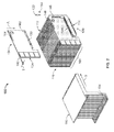
- Figure 1 is a perspective view of a power connector formed in accordance with an exemplary embodiment of the present invention.
- Figure 2 is an exploded view of the connector of Figure 1.
- Figure 3 is a side elevation view of the first side of an exemplary wafer formed in accordance with an exemplary embodiment of the present invention.
- Figure 4 is a side elevation view of the second side of the wafer shown in Figure 3.
- Figure 5 is a cross sectional view of the wafer taken along line 5-5 in Figure 3.
- Figure 1 illustrates a power connector 100 formed in accordance with an exemplary embodiment of the present invention.
- the connector 100 is configured to reduce fluctuations in power transmitted through the connector 100.
- the connector 100 exhibits some of the characteristics of a capacitor while using only materials and components necessary to transmit power through the connector 100.
- the connector 100 will be described in terms of a right angle connector, however, it is to be understood that this is for purposes of illustration only and no limitation is intended thereby. In alternative embodiments, other configurations may be employed.
- the connector 100 includes a housing 102 and a plurality of electrical wafers 104.
- the housing 102 includes a cover portion 110 and a base portion 112.
- the base 112 includes a plurality of contacts 114 that form a daughter card or daughter board interface 120.
- the contacts 114 have a resilient upper end 122 ( Figure 2) that receives an edge of the wafer 104.
- the cover 110 includes an upper shroud 130 and a lower shroud 132 that partially cover a mating end of the connector 100.
- Each of the wafers 104 includes a backplane edge 134 and these edges combine to form a backplane connector interface 140.
- FIG. 2 illustrates an exploded view of the connector 100.
- the housing base 112 includes a plurality of slots 144.
- the wafers 104 are received into the slots 144 with a card edge connection.
- An alignment slot 146 is formed into the back wall 148 of the housing base 112 at each slot 144.
- Each wafer 104 includes a daughter card or daughter board edge 150 that is received in the upper ends 122 of the contacts 114.
- the contacts 114 extend through the housing base 112 to become part of the daughter board interface 120.
- the wafers 104 are inserted into the slots 144 in a downward direction indicated by the arrow A.
- the housing cover 110 includes a plurality of alignment apertures 154 that receive the backplane edges 134 of the wafers 104.
- the apertures 154 hold and stabilize the wafers 104 in the slots 144 of the housing base 112.
- the housing cover 110 is attached by sliding the cover 110 onto the base 112 in the direction of arrow B so that the backplane edges 134 of the wafers 104 extend through the apertures 154.
- Each wafer 104 includes a planar sheet of a dielectric material 160 that has a first side 162 and a second side 164 that is opposite and substantially parallel to the first side 162.
- the wafer 104 is a printed circuit board and the dielectric material 160 is a material such as FR4.
- the dielectric material 160 has a thickness T that is substantially uniform between the first and second sides 162 and 164, respectively.
- the dielectric material is a printed circuit board. In other embodiments, any insulating material having a sufficiently high dielectric constant may be used.
- the backplane edge 134 and the daughter board edge 150 are substantially perpendicular to each other. However, in alternative embodiments, it is contemplated that edges 134 and 150 may intersect at other than a right angle, or the edges 134 and 150 may be parallel.
- Figure 3 illustrates a side elevation view of the first side 162 of the wafer 104.
- Figure 4 illustrates a side elevation view of the second side 164 of the wafer 104.
- the first side 162 includes a number of power traces 170, 172, 174, and a ground trace 176.
- the traces 170, 172, 174, and 176 extend between power contact pads 180, 182, 184, and a ground contact pad 186 arranged along the backplane edge 134, and power contact pads 190, 192, 194, and a ground contact pad 196 arranged along the daughter board edge 150.
- the ends 122 of contacts 114 engage the contact pads 190, 192, 194, and 196 along the daughter board edge 150 to connect each wafer to the daughter board interface 120.
- three power traces are present. It is to be understood however, that in other embodiments a fewer or greater number of power traces may be present.
- the second side 164 includes a single ground trace or ground plane 200.
- the power traces 170, 172, 174 and the ground trace 176 on the first side 162 are shown in phantom outline.
- Vias 202 extend through the dielectric material 160 to connect the ground plane 200 to the ground trace 176 on the first side 162 of the wafer 104.
- the ground trace 200 is substantially parallel to the power traces 170, 172, and 174 on the first side 162 of the wafer 104.
- the second side 164 is without contact pads at the backplane edge 134.
- the wafer 104 as depicted in Figures 3 and 4 exemplifies an embodiment wherein contacts are provided that make connections only with the first side 162, of the wafer 104. In such applications, a ground trace 176 is provided on the first side 162 to make the ground reference available to the backplane and daughter board.
- the power traces 170, 172, 174 at least partially overlap the ground trace 200. That is, at least a portion of the surface area of each power trace 170, 172, and 174 on the first side 162 of the wafer 104 coincides with a portion of the surface area of the ground trace 200 on the second side 164 in a direction substantially perpendicular to the surfaces of the first and second sides 162 and 164 respectively.
- the connector 100 provides decoupling with a low inductance power ⁇ ground couple inside the connector, using only the materials used for power transmission through the connector 100.
- the connector 100 acts as a capacitor that stores and releases energy to reduce voltage fluctuations in the power transmitted through the connector 100.
- the characteristics of a capacitor are achieved by the placement of the power traces 170, 172, and 174 on one side 162 and the ground trace 200 on the opposite side 164 of the wafer 104, and separating the power and ground traces by the dielectric material 160. Effectively, each wafer 104 is provided with an energy storage device integrally formed therewith.
- the dielectric material 160 and the thickness T are selected to provide a usable charge storage capability in the connector 100.
- the dielectric material 160 and the thickness T are selected such that the ratio of the dielectric constant for the dielectric material 160 to the thickness T is about four hundred or greater.
- the dielectric material 160 is comprised of a PCB material having a dielectric constant of about four, and formed with a thickness T of about 0.254 mm (0.010 inch).
- Each power trace 170, 172, and 174 forms a decoupling capacitor within the connector 100.
- the total capacitance of the connector 100 is the sum of the capacitance of the individual power traces 170, 172, and 174.
- the capacitance of each power trace 170, 172, 174 is determined by the equation:
- C is the capacitance
- A is the surface area of the power trace
- D is the thickness of the dielectric material
- E is the dielectric constant of the dielectric material.
- Figure 5 illustrates a cross section of the wafer 104 taken along the line 5-5 shown in Figure 3.
- the dielectric material 160 has a thickness T and separates the power traces 170, 172, 174 and the ground trace 200.
- the ground trace 176 on the first side 162 of the dielectric material is connected to the ground trace 200 through the vias 202 ( Figures 3 and 4) and thus the ground trace 176 is at the same electrical potential as the ground trace 200.
- the power traces 170, 172, 174 have a different electrical potential than the ground traces 200 and 176.
- the surface area A in the above equation represents the surface area of the power traces 170, 172, 174 that is parallel to the ground trace 200 and that overlaps the ground trace 200.
- the performance of the connector 100 is improved as capacitance increases. That is, as capacitance increases, so does the energy storage capacity of the connector 100.
- a thinner dielectric layer and/or a dielectric material having a higher dielectric constant increases capacitance.
- the dielectric material and its thickness are selected to provide a relatively high capacitance.
- the table below illustrates various dielectric thicknesses (measured in inches) and dielectric constant combinations that yield a dielectric constant-to-thickness ratio of 400 to 1.
- the storage and release of energy in the connector 100 occurs automatically in response to fluctuations in power being transmitted through the connector 100.
- the embodiments thus described provide a power connector 100 that reduces fluctuations in power transmitted through the connector 100.
- the connector 100 exhibits some of the characteristics of a capacitor, but uses only materials and components necessary to transmit power through the connector 100.
- the connector 100 avoids the use of decoupling capacitors external to the connector 100 thereby saving space on the backplane and daughter boards.
- the connector 100 may be in the form of a right angle connector.
Landscapes
- Details Of Connecting Devices For Male And Female Coupling (AREA)
Abstract
Description
- The invention relates generally to electrical connectors and, more particularly, to a power connector that reduces fluctuations in transmitted power.
- In some power distribution systems, power is distributed from a central power supply or power source connected to a backplane and then distributed from a power plane to a daughter board through a power connector. In some applications, the power connector includes a number of wafers that typically are about two millimeters in thickness. Power is transmitted through traces on the wafers.
- The daughter board includes active components that use the power. Ideally, the power source would deliver its rated power at all times. However, when the power consuming devices include switching devices, invariably, the changing loads cause a fluctuation in the power output of the power source. In addition, the inductance of system components such as wires, traces, and connectors, etc., make it more difficult to avoid localized power plane voltage fluctuations. In particular, inductance within the power connector itself is sought to be reduced.
- When chips or components on the daughter board switch rapidly, there is a need for a mechanism that can maintain the power supply voltage to the daughter board. Traditionally, the problems associated with power source fluctuations have been addressed through the use of decoupling capacitors in an effort to prevent large voltage drops associated with component switching. If the voltage drops below a required range, the switching of the components is affected such that the components do not function properly. The capacitors are placed on the backplane near the power connectors so that when rapid switching occurs, the capacitors store some of the energy, after which the stored energy can be drawn from the capacitor and made available to the system in an effort to maintain system voltages. Capacitors are also used on the daughter board to smooth out power fluctuations.
- Generally, the decoupling capacitors are more effective when they are in close proximity to the power connectors. The decoupling capacitors could be placed inside the power connector; however this increases the size and complexity of the connector. It would be desirable to move the decoupling effect into the power connector without the use of additional components that increase the size and complexity of the power connector.
- This problem is solved by a power connector according to the invention.
- The invention is a power connector comprising a housing and an electrical wafer mounted in the housing. The wafer includes a dielectric material having a thickness between a first side and a second side. The second side is opposite the first side and substantially parallel to the first side. A power trace is located on the first side of the wafer, and a ground trace is located on the second side of the wafer. The power trace at least partially overlaps the ground trace, and the thickness of the dielectric material is such that the power trace and the ground trace form a decoupling capacitor that reduces fluctuations in the power transmitted through the connector.
- The invention will now be described by way of example with reference to the accompanying drawings wherein:
- Figure 1 is a perspective view of a power connector formed in accordance with an exemplary embodiment of the present invention.
- Figure 2 is an exploded view of the connector of Figure 1.
- Figure 3 is a side elevation view of the first side of an exemplary wafer formed in accordance with an exemplary embodiment of the present invention.
- Figure 4 is a side elevation view of the second side of the wafer shown in Figure 3.
- Figure 5 is a cross sectional view of the wafer taken along line 5-5 in Figure 3.
- Figure 1 illustrates a
power connector 100 formed in accordance with an exemplary embodiment of the present invention. Theconnector 100 is configured to reduce fluctuations in power transmitted through theconnector 100. Theconnector 100 exhibits some of the characteristics of a capacitor while using only materials and components necessary to transmit power through theconnector 100. Theconnector 100 will be described in terms of a right angle connector, however, it is to be understood that this is for purposes of illustration only and no limitation is intended thereby. In alternative embodiments, other configurations may be employed. - The
connector 100 includes ahousing 102 and a plurality ofelectrical wafers 104. Thehousing 102 includes acover portion 110 and abase portion 112. Thebase 112 includes a plurality ofcontacts 114 that form a daughter card ordaughter board interface 120. Thecontacts 114 have a resilient upper end 122 (Figure 2) that receives an edge of thewafer 104. Thecover 110 includes anupper shroud 130 and alower shroud 132 that partially cover a mating end of theconnector 100. Each of thewafers 104 includes abackplane edge 134 and these edges combine to form abackplane connector interface 140. - Figure 2 illustrates an exploded view of the
connector 100. Thehousing base 112 includes a plurality ofslots 144. Thewafers 104 are received into theslots 144 with a card edge connection. Analignment slot 146 is formed into theback wall 148 of thehousing base 112 at eachslot 144. Eachwafer 104 includes a daughter card ordaughter board edge 150 that is received in theupper ends 122 of thecontacts 114. Thecontacts 114 extend through thehousing base 112 to become part of thedaughter board interface 120. Thewafers 104 are inserted into theslots 144 in a downward direction indicated by the arrow A. Thehousing cover 110 includes a plurality ofalignment apertures 154 that receive thebackplane edges 134 of thewafers 104. Theapertures 154 hold and stabilize thewafers 104 in theslots 144 of thehousing base 112. After thewafers 104 are installed in thehousing base 112, thehousing cover 110 is attached by sliding thecover 110 onto thebase 112 in the direction of arrow B so that thebackplane edges 134 of thewafers 104 extend through theapertures 154. - Each
wafer 104 includes a planar sheet of adielectric material 160 that has afirst side 162 and asecond side 164 that is opposite and substantially parallel to thefirst side 162. In one embodiment, thewafer 104 is a printed circuit board and thedielectric material 160 is a material such as FR4. Thedielectric material 160 has a thickness T that is substantially uniform between the first andsecond sides backplane edge 134 and thedaughter board edge 150 are substantially perpendicular to each other. However, in alternative embodiments, it is contemplated thatedges edges - Figure 3 illustrates a side elevation view of the
first side 162 of thewafer 104. Figure 4 illustrates a side elevation view of thesecond side 164 of thewafer 104. Thefirst side 162 includes a number ofpower traces ground trace 176. Thetraces power contact pads ground contact pad 186 arranged along thebackplane edge 134, andpower contact pads ground contact pad 196 arranged along thedaughter board edge 150. Theends 122 of contacts 114 (Figure 2) engage thecontact pads daughter board edge 150 to connect each wafer to thedaughter board interface 120. In the embodiment shown in Figure 3, three power traces are present. It is to be understood however, that in other embodiments a fewer or greater number of power traces may be present. - The
second side 164 includes a single ground trace orground plane 200. The power traces 170, 172, 174 and theground trace 176 on thefirst side 162 are shown in phantom outline.Vias 202 extend through thedielectric material 160 to connect theground plane 200 to theground trace 176 on thefirst side 162 of thewafer 104. Theground trace 200 is substantially parallel to the power traces 170, 172, and 174 on thefirst side 162 of thewafer 104. Thesecond side 164 is without contact pads at thebackplane edge 134. Thewafer 104 as depicted in Figures 3 and 4 exemplifies an embodiment wherein contacts are provided that make connections only with thefirst side 162, of thewafer 104. In such applications, aground trace 176 is provided on thefirst side 162 to make the ground reference available to the backplane and daughter board. - The power traces 170, 172, 174 at least partially overlap the
ground trace 200. That is, at least a portion of the surface area of eachpower trace first side 162 of thewafer 104 coincides with a portion of the surface area of theground trace 200 on thesecond side 164 in a direction substantially perpendicular to the surfaces of the first andsecond sides - The
connector 100 provides decoupling with a low inductance power ― ground couple inside the connector, using only the materials used for power transmission through theconnector 100. When switching of power consuming components occurs, theconnector 100 acts as a capacitor that stores and releases energy to reduce voltage fluctuations in the power transmitted through theconnector 100. The characteristics of a capacitor are achieved by the placement of the power traces 170, 172, and 174 on oneside 162 and theground trace 200 on theopposite side 164 of thewafer 104, and separating the power and ground traces by thedielectric material 160. Effectively, eachwafer 104 is provided with an energy storage device integrally formed therewith. Thedielectric material 160 and the thickness T are selected to provide a usable charge storage capability in theconnector 100. Thedielectric material 160 and the thickness T are selected such that the ratio of the dielectric constant for thedielectric material 160 to the thickness T is about four hundred or greater. In an exemplary embodiment, thedielectric material 160 is comprised of a PCB material having a dielectric constant of about four, and formed with a thickness T of about 0.254 mm (0.010 inch). - Each
power trace connector 100. The total capacitance of theconnector 100 is the sum of the capacitance of the individual power traces 170, 172, and 174. The capacitance of eachpower trace -

- where: C is the capacitance, A is the surface area of the power trace, D is the thickness of the dielectric material, and E is the dielectric constant of the dielectric material.
- Figure 5 illustrates a cross section of the
wafer 104 taken along the line 5-5 shown in Figure 3. Thedielectric material 160 has a thickness T and separates the power traces 170, 172, 174 and theground trace 200. Theground trace 176 on thefirst side 162 of the dielectric material is connected to theground trace 200 through the vias 202 (Figures 3 and 4) and thus theground trace 176 is at the same electrical potential as theground trace 200. The power traces 170, 172, 174 have a different electrical potential than the ground traces 200 and 176. The surface area A in the above equation represents the surface area of the power traces 170, 172, 174 that is parallel to theground trace 200 and that overlaps theground trace 200. The performance of theconnector 100 is improved as capacitance increases. That is, as capacitance increases, so does the energy storage capacity of theconnector 100. - As seen from the equation above, a thinner dielectric layer and/or a dielectric material having a higher dielectric constant increases capacitance. The dielectric material and its thickness are selected to provide a relatively high capacitance. For instance, the table below illustrates various dielectric thicknesses (measured in inches) and dielectric constant combinations that yield a dielectric constant-to-thickness ratio of 400 to 1.
-
Thickness Dielectric Constant 0.254 mm 0.01 (inch) 4 0.508 mm 0.02 (inch) 8 1.016 mm 0.04 (inch) 16 0.127 mm 0.005 (inch) 2 - In operation, the storage and release of energy in the
connector 100 occurs automatically in response to fluctuations in power being transmitted through theconnector 100. - The embodiments thus described provide a
power connector 100 that reduces fluctuations in power transmitted through theconnector 100. Theconnector 100 exhibits some of the characteristics of a capacitor, but uses only materials and components necessary to transmit power through theconnector 100. Theconnector 100 avoids the use of decoupling capacitors external to theconnector 100 thereby saving space on the backplane and daughter boards. Theconnector 100 may be in the form of a right angle connector.
Claims (5)
- A power connector (100) comprising a housing (102) and an electrical wafer (104) mounted in said housing (102), said wafer (104) including a dielectric material (160) having a thickness (T) between a first side (162) and a second side (164), said second side (164) being opposite said first side (162) and substantially parallel to said first side (162), a power trace (170, 172, 174) located on said first side (162) of said wafer (104), and a ground trace (200) located on said second side (164) of said wafer (104), said power trace (170, 172, 174) at least partially overlapping said ground trace (200), wherein the thickness (T) is such that said power trace and said ground trace (200) form a decoupling capacitor that reduces fluctuations in the power transmitted through the connector (100).
- The power connector (100) of claim 1, wherein the thickness (T) of the dielectric material (160) is no greater than about 0.254 mm. (0.010 inch).
- The power connector of claim 1 or 2, wherein said first side (162) includes a ground trace (176) and a plurality of vias (202) connecting said ground trace (176) on said first side (162) to said ground trace (200) on said second side (164).
- The power connector (100) of any preceding claim, wherein said dielectric material (160) and said thickness (T) are selected such that a ratio of a dielectric constant for said dielectric material (160) to said thickness (T) is about four hundred to one or greater.
- The power connector (100) of any preceding claim, wherein said housing (102) comprises a base portion (112) and a cover portion (110), said base portion (112) including an alignment slot (144), said wafer (104) having an edge (150) receivable in said alignment slot (144), and said cover portion (110) including an aperture (154) configured to receive and stabilize said wafer (104).
Applications Claiming Priority (1)
| Application Number | Priority Date | Filing Date | Title |
|---|---|---|---|
| US11/190,746 US7168988B1 (en) | 2005-07-27 | 2005-07-27 | Power connector with integrated decoupling |
Publications (2)
| Publication Number | Publication Date |
|---|---|
| EP1748519A2 true EP1748519A2 (en) | 2007-01-31 |
| EP1748519A3 EP1748519A3 (en) | 2007-03-28 |
Family
ID=37310794
Family Applications (1)
| Application Number | Title | Priority Date | Filing Date |
|---|---|---|---|
| EP06117791A Withdrawn EP1748519A3 (en) | 2005-07-27 | 2006-07-25 | Power connector with integrated decoupling |
Country Status (3)
| Country | Link |
|---|---|
| US (1) | US7168988B1 (en) |
| EP (1) | EP1748519A3 (en) |
| CN (1) | CN1909299B (en) |
Families Citing this family (9)
| Publication number | Priority date | Publication date | Assignee | Title |
|---|---|---|---|---|
| US8157595B2 (en) * | 2010-07-13 | 2012-04-17 | Tyco Electronics Corporation | Ground shield for an electrical connector |
| CN102761012B (en) * | 2012-07-25 | 2014-10-08 | 贵州航天电器股份有限公司 | Combining and positioning structure for modular connector |
| US9196985B2 (en) | 2014-01-09 | 2015-11-24 | Tyco Electronics Corporation | Configurable electrical connector assembly |
| US9583851B2 (en) * | 2015-06-11 | 2017-02-28 | Lenovo Enterprise Solutions (Singapore) Pte. Ltd. | Orthogonal card edge connector |
| US9559446B1 (en) * | 2016-01-12 | 2017-01-31 | Tyco Electronics Corporation | Electrical connector having a signal contact section and a power contact section |
| CN108336598A (en) * | 2018-01-31 | 2018-07-27 | 郑州云海信息技术有限公司 | A kind of connector construction with decoupling function |
| KR102828625B1 (en) * | 2020-01-31 | 2025-07-04 | 에스케이하이닉스 주식회사 | Package substrate having power trace pattern and ground trace pattern, and semiconductor package including the same |
| WO2024189600A1 (en) * | 2023-03-15 | 2024-09-19 | Te Connectivity Solutions Gmbh | Optical backplane connector system |
| US20250337198A1 (en) * | 2024-04-24 | 2025-10-30 | Te Connectivity Solutions Gmbh | Contact wafer for a connector assembly having a signal conditioning module |
Family Cites Families (9)
| Publication number | Priority date | Publication date | Assignee | Title |
|---|---|---|---|---|
| US6824391B2 (en) * | 2000-02-03 | 2004-11-30 | Tyco Electronics Corporation | Electrical connector having customizable circuit board wafers |
| US6540522B2 (en) * | 2001-04-26 | 2003-04-01 | Tyco Electronics Corporation | Electrical connector assembly for orthogonally mating circuit boards |
| US6848944B2 (en) * | 2001-11-12 | 2005-02-01 | Fci Americas Technology, Inc. | Connector for high-speed communications |
| US6638110B1 (en) * | 2002-05-22 | 2003-10-28 | Hon Hai Precision Ind. Co., Ltd. | High density electrical connector |
| US6808399B2 (en) * | 2002-12-02 | 2004-10-26 | Tyco Electronics Corporation | Electrical connector with wafers having split ground planes |
| JP2005032529A (en) * | 2003-07-10 | 2005-02-03 | Jst Mfg Co Ltd | High-speed transmission connector |
| US6808419B1 (en) * | 2003-08-29 | 2004-10-26 | Hon Hai Precision Ind. Co., Ltd. | Electrical connector having enhanced electrical performance |
| US7044794B2 (en) * | 2004-07-14 | 2006-05-16 | Tyco Electronics Corporation | Electrical connector with ESD protection |
| US7175445B2 (en) * | 2004-08-31 | 2007-02-13 | Tyco Electronics Corporation | Electrical connector power wafers |
-
2005
- 2005-07-27 US US11/190,746 patent/US7168988B1/en not_active Expired - Lifetime
-
2006
- 2006-07-25 EP EP06117791A patent/EP1748519A3/en not_active Withdrawn
- 2006-07-27 CN CN2006101257259A patent/CN1909299B/en not_active Expired - Fee Related
Also Published As
| Publication number | Publication date |
|---|---|
| EP1748519A3 (en) | 2007-03-28 |
| CN1909299B (en) | 2012-02-01 |
| US20070026737A1 (en) | 2007-02-01 |
| US7168988B1 (en) | 2007-01-30 |
| CN1909299A (en) | 2007-02-07 |
Similar Documents
| Publication | Publication Date | Title |
|---|---|---|
| EP2034806B1 (en) | Circuit board device, wiring board interconnection method | |
| US7123465B2 (en) | Decoupling capacitor for an integrated circuit and method of manufacturing thereof | |
| US7365990B2 (en) | Circuit board arrangement including heat dissipater | |
| CN107850823B (en) | Camera module | |
| US20070268677A1 (en) | System and method for processor power delivery and thermal management | |
| US5532907A (en) | Computer system with improved power bus | |
| US20020114129A1 (en) | Ultra-low impedance power interconnection system for electronic packages | |
| US9537237B2 (en) | System to improve an in-line memory module | |
| US8333597B2 (en) | Connector and interposer using connector | |
| US7549871B2 (en) | Connector with dual compression polymer and flexible contact array | |
| TWI267092B (en) | Anisotropic conductive sheet | |
| US7168988B1 (en) | Power connector with integrated decoupling | |
| US20080119070A1 (en) | Electrical Connector | |
| WO2018168352A1 (en) | Receptacle | |
| US20040264148A1 (en) | Method and system for fan fold packaging | |
| US6612851B1 (en) | Electrical connector assembly for printed circuit boards | |
| KR102766733B1 (en) | Electrical connection module, socket with electrical connection module, printed circuit board with electrical connection module and manufacturing method of electrical connection module | |
| TW461157B (en) | Low inductance connector with enhanced capacitively coupled contacts for power applications | |
| US20150201496A1 (en) | Radio module and relevant manufacturing method | |
| US10499545B2 (en) | Stacked module, stacking method, cooling/feeding mechanism, and stacked module mounting board | |
| US20060264112A1 (en) | Semiconductor device having a module board | |
| WO2018168336A1 (en) | Signal transmission module | |
| US9941567B2 (en) | Integrated PCB interconnect system | |
| US6729896B2 (en) | Electrical connector with distortion-resistant cover | |
| US20080202802A1 (en) | Printed circuit board module having two printed circuit boards for mounting inline package elements and adhibit elements respectively |
Legal Events
| Date | Code | Title | Description |
|---|---|---|---|
| PUAI | Public reference made under article 153(3) epc to a published international application that has entered the european phase |
Free format text: ORIGINAL CODE: 0009012 |
|
| AK | Designated contracting states |
Kind code of ref document: A2 Designated state(s): AT BE BG CH CY CZ DE DK EE ES FI FR GB GR HU IE IS IT LI LT LU LV MC NL PL PT RO SE SI SK TR |
|
| AX | Request for extension of the european patent |
Extension state: AL BA HR MK YU |
|
| PUAL | Search report despatched |
Free format text: ORIGINAL CODE: 0009013 |
|
| AK | Designated contracting states |
Kind code of ref document: A3 Designated state(s): AT BE BG CH CY CZ DE DK EE ES FI FR GB GR HU IE IS IT LI LT LU LV MC NL PL PT RO SE SI SK TR |
|
| AX | Request for extension of the european patent |
Extension state: AL BA HR MK YU |
|
| 17P | Request for examination filed |
Effective date: 20070924 |
|
| AKX | Designation fees paid |
Designated state(s): DE FR GB |
|
| 17Q | First examination report despatched |
Effective date: 20071115 |
|
| STAA | Information on the status of an ep patent application or granted ep patent |
Free format text: STATUS: THE APPLICATION IS DEEMED TO BE WITHDRAWN |
|
| 18D | Application deemed to be withdrawn |
Effective date: 20080326 |