EP1746566A1 - An organic light emitting display device and a method for generating scan signals for driving an organic light emitting display device having a scan driver - Google Patents
An organic light emitting display device and a method for generating scan signals for driving an organic light emitting display device having a scan driver Download PDFInfo
- Publication number
- EP1746566A1 EP1746566A1 EP06117723A EP06117723A EP1746566A1 EP 1746566 A1 EP1746566 A1 EP 1746566A1 EP 06117723 A EP06117723 A EP 06117723A EP 06117723 A EP06117723 A EP 06117723A EP 1746566 A1 EP1746566 A1 EP 1746566A1
- Authority
- EP
- European Patent Office
- Prior art keywords
- flip
- transistor
- signal
- flops
- scan
- Prior art date
- Legal status (The legal status is an assumption and is not a legal conclusion. Google has not performed a legal analysis and makes no representation as to the accuracy of the status listed.)
- Granted
Links
Images



Classifications
-
- G—PHYSICS
- G09—EDUCATION; CRYPTOGRAPHY; DISPLAY; ADVERTISING; SEALS
- G09G—ARRANGEMENTS OR CIRCUITS FOR CONTROL OF INDICATING DEVICES USING STATIC MEANS TO PRESENT VARIABLE INFORMATION
- G09G3/00—Control arrangements or circuits, of interest only in connection with visual indicators other than cathode-ray tubes
- G09G3/20—Control arrangements or circuits, of interest only in connection with visual indicators other than cathode-ray tubes for presentation of an assembly of a number of characters, e.g. a page, by composing the assembly by combination of individual elements arranged in a matrix no fixed position being assigned to or needed to be assigned to the individual characters or partial characters
- G09G3/22—Control arrangements or circuits, of interest only in connection with visual indicators other than cathode-ray tubes for presentation of an assembly of a number of characters, e.g. a page, by composing the assembly by combination of individual elements arranged in a matrix no fixed position being assigned to or needed to be assigned to the individual characters or partial characters using controlled light sources
- G09G3/30—Control arrangements or circuits, of interest only in connection with visual indicators other than cathode-ray tubes for presentation of an assembly of a number of characters, e.g. a page, by composing the assembly by combination of individual elements arranged in a matrix no fixed position being assigned to or needed to be assigned to the individual characters or partial characters using controlled light sources using electroluminescent panels
-
- G—PHYSICS
- G11—INFORMATION STORAGE
- G11C—STATIC STORES
- G11C19/00—Digital stores in which the information is moved stepwise, e.g. shift registers
- G11C19/28—Digital stores in which the information is moved stepwise, e.g. shift registers using semiconductor elements
-
- G—PHYSICS
- G09—EDUCATION; CRYPTOGRAPHY; DISPLAY; ADVERTISING; SEALS
- G09G—ARRANGEMENTS OR CIRCUITS FOR CONTROL OF INDICATING DEVICES USING STATIC MEANS TO PRESENT VARIABLE INFORMATION
- G09G3/00—Control arrangements or circuits, of interest only in connection with visual indicators other than cathode-ray tubes
- G09G3/20—Control arrangements or circuits, of interest only in connection with visual indicators other than cathode-ray tubes for presentation of an assembly of a number of characters, e.g. a page, by composing the assembly by combination of individual elements arranged in a matrix no fixed position being assigned to or needed to be assigned to the individual characters or partial characters
- G09G3/22—Control arrangements or circuits, of interest only in connection with visual indicators other than cathode-ray tubes for presentation of an assembly of a number of characters, e.g. a page, by composing the assembly by combination of individual elements arranged in a matrix no fixed position being assigned to or needed to be assigned to the individual characters or partial characters using controlled light sources
- G09G3/30—Control arrangements or circuits, of interest only in connection with visual indicators other than cathode-ray tubes for presentation of an assembly of a number of characters, e.g. a page, by composing the assembly by combination of individual elements arranged in a matrix no fixed position being assigned to or needed to be assigned to the individual characters or partial characters using controlled light sources using electroluminescent panels
- G09G3/32—Control arrangements or circuits, of interest only in connection with visual indicators other than cathode-ray tubes for presentation of an assembly of a number of characters, e.g. a page, by composing the assembly by combination of individual elements arranged in a matrix no fixed position being assigned to or needed to be assigned to the individual characters or partial characters using controlled light sources using electroluminescent panels semiconductive, e.g. using light-emitting diodes [LED]
- G09G3/3208—Control arrangements or circuits, of interest only in connection with visual indicators other than cathode-ray tubes for presentation of an assembly of a number of characters, e.g. a page, by composing the assembly by combination of individual elements arranged in a matrix no fixed position being assigned to or needed to be assigned to the individual characters or partial characters using controlled light sources using electroluminescent panels semiconductive, e.g. using light-emitting diodes [LED] organic, e.g. using organic light-emitting diodes [OLED]
- G09G3/3266—Details of drivers for scan electrodes
-
- G—PHYSICS
- G09—EDUCATION; CRYPTOGRAPHY; DISPLAY; ADVERTISING; SEALS
- G09G—ARRANGEMENTS OR CIRCUITS FOR CONTROL OF INDICATING DEVICES USING STATIC MEANS TO PRESENT VARIABLE INFORMATION
- G09G2300/00—Aspects of the constitution of display devices
- G09G2300/02—Composition of display devices
- G09G2300/026—Video wall, i.e. juxtaposition of a plurality of screens to create a display screen of bigger dimensions
-
- G—PHYSICS
- G09—EDUCATION; CRYPTOGRAPHY; DISPLAY; ADVERTISING; SEALS
- G09G—ARRANGEMENTS OR CIRCUITS FOR CONTROL OF INDICATING DEVICES USING STATIC MEANS TO PRESENT VARIABLE INFORMATION
- G09G2300/00—Aspects of the constitution of display devices
- G09G2300/04—Structural and physical details of display devices
- G09G2300/0404—Matrix technologies
- G09G2300/0408—Integration of the drivers onto the display substrate
-
- G—PHYSICS
- G09—EDUCATION; CRYPTOGRAPHY; DISPLAY; ADVERTISING; SEALS
- G09G—ARRANGEMENTS OR CIRCUITS FOR CONTROL OF INDICATING DEVICES USING STATIC MEANS TO PRESENT VARIABLE INFORMATION
- G09G2300/00—Aspects of the constitution of display devices
- G09G2300/04—Structural and physical details of display devices
- G09G2300/0404—Matrix technologies
- G09G2300/0417—Special arrangements specific to the use of low carrier mobility technology
-
- G—PHYSICS
- G09—EDUCATION; CRYPTOGRAPHY; DISPLAY; ADVERTISING; SEALS
- G09G—ARRANGEMENTS OR CIRCUITS FOR CONTROL OF INDICATING DEVICES USING STATIC MEANS TO PRESENT VARIABLE INFORMATION
- G09G2300/00—Aspects of the constitution of display devices
- G09G2300/04—Structural and physical details of display devices
- G09G2300/0421—Structural details of the set of electrodes
- G09G2300/0426—Layout of electrodes and connections
-
- G—PHYSICS
- G09—EDUCATION; CRYPTOGRAPHY; DISPLAY; ADVERTISING; SEALS
- G09G—ARRANGEMENTS OR CIRCUITS FOR CONTROL OF INDICATING DEVICES USING STATIC MEANS TO PRESENT VARIABLE INFORMATION
- G09G2330/00—Aspects of power supply; Aspects of display protection and defect management
- G09G2330/02—Details of power systems and of start or stop of display operation
- G09G2330/021—Power management, e.g. power saving
Definitions
- the present invention relates to an organic light emitting display (OLED) device and, more particularly, to a system on panel (SOP) type scan driver which generates scan signals for selecting pixels located on a display region, and an OLED device having the same.
- OLED organic light emitting display
- SOP system on panel
- FPDs flat panel displays
- CRTs cathode ray tubes
- LCDs liquid crystal displays
- FEDs field emission displays
- PDPs plasma display panels
- OLEDs organic light emitting displays
- the PDP can have a large screen but has low luminance and poor luminous efficiency resulting in high power consumption
- the LCD has a relatively slow response speed and consumes a lot of power since it employs a backlight.
- the OLED makes use of an organic material to emit light, it has a wider viewing angle and faster response speed than the LCD. Also, the OLED is an emissive display that obtains good contrast and visibility. Further, the OLED enables lower power consumption and can be made thin and lightweight because it needs no backlight.
- an electroluminescent (EL) panel for a glass substrate are limited due to fabricating process limitations and the OLED may not be easily constructed to have a large screen. Also, if the screen is large, there is a greater probability of a defect occurring somewhere on the screen and thus a reduction in yield is unavoidable. Further, it is difficult to obtain uniformity across the screen.
- EL electroluminescent
- a tiling technique was developed.
- EL panels are bonded together like tiles to form a single panel.
- Each of the EL panels includes pixels to display a predetermined image similar to a conventional OLED.
- a scan driver applies a scan signal to enable the pixels
- a data driver applies a data signal to a selected pixel.
- an emission control driver applies an emission control signal to each of the pixels in order to control the exact programming of the data signal and the time taken for an emission operation.
- the scan driver, the data driver, and the emission control driver which transmit various signals to drive the EL panels, can be electrically coupled to each of the EL panels in various manners.
- the scan driver, the data driver, and the emission control driver may be mounted as chips on a tape carrier package (TCP) that is bonded and electrically coupled to each of the EL panels.
- the drivers may be mounted as chips on a flexible printed circuit (FPC) or a film that is bonded and electrically coupled to each of the EL panels.
- FPC flexible printed circuit
- COF chip on film
- the drivers are directly mounted on a glass substrate of the EL panel. This method is referred to as a chip on glass (COG) technique.
- SOP system on panel
- each EL panel is formed as an SOP, it is easy to bond the EL panels to one another. Also, the SOP technique enables the area of drivers to be reduced and cost and labor for designing integrated circuits (ICs) of the respective drivers to be saved.
- ICs integrated circuits
- the data driver is formed separately as an IC using complementary metal oxide semiconductor (CMOS) technology and subsequently coupled to the EL panel, while the scan driver and/or the emission control driver are formed within the EL panel.
- CMOS complementary metal oxide semiconductor
- the present invention therefore, provides a scan driver for an organic light emitting display (OLED) device, which is designed as a system on panel (SOP) type in an electroluminescent (EL) panel and generates scan signals for selecting pixels.
- OLED organic light emitting display
- SOP system on panel
- EL electroluminescent
- an OLED device includes a display region having pixels and displaying a predetermined image, a scan driver having flip-flops and applying a scan signal to sequentially select the pixels, a data driver applying a data signal to the pixels that are selected by the scan signal, and an emission control driver applying an emission control signal to control an emission operation of the pixels, wherein each of the flip-flops of the scan driver includes a first transistor, coupled between a positive power supply voltage terminal and a first node, and turned on/off according to a control signal applied to a gate terminal of the first transistor, a second transistor, coupled between the first node and an inverted control signal line and turned on/off according to a voltage at a second node coupled to a gate terminal of the second transistor, and a third transistor having a first electrode and a second electrode, wherein the first electrode of the third transistor is coupled to the second node and an input signal applied to the second electrode of the third transistor is transmitted to the first electrode of the third transistor according to the control signal applied to
- an organic light emitting display device comprises a display region having pixels for displaying a predetermined image; a scan driver having flip-flops and applying a scan signal to select the pixels; a data driver for applying a data signal to selected pixels; and an emission control driver for applying an emission control signal to control an emission operation of the pixels, wherein at least one of the flip-flops of the scan driver includes:
- an OLED device in another exemplary embodiment of the present invention, includes a display region having pixels and displaying a predetermined image, a scan driver having flip-flops and applying a scan signal to sequentially select the pixels, a data driver applying a data signal to the pixels that are selected by the scan signal, and an emission control driver applying an emission control signal to control an emission operation of the pixels, wherein each of the flip-flops of the scan driver includes a first transistor, coupled between a positive power supply voltage terminal and a first node, and turned on/off according to a control signal applied to a gate terminal of the first transistor, a second transistor, coupled between the first node and one of a clock signal line and an inverted clock signal line and turned on/off according to a voltage at the second node coupled to a gate terminal of the second transistor, a third transistor having a first electrode and a second electrode, wherein the first electrode of the third transistor is coupled to a second node and an input signal applied to the second electrode of the third transistor is transmitted to the first electrode of the third
- an organic light emitting display device comprises a display region having pixels for displaying a predetermined image; a scan driver having flip-flops for applying a scan signal to select the pixels; a data driver for applying a data signal to selected pixels; and an emission control driver for applying an emission control signal for controlling an emission operation of the pixels, wherein at least one of the flip-flops of the scan driver includes:
- the control signal input portion may include a fourth transistor, coupled between a negative power supply voltage terminal and the gate terminal of the first transistor and the gate terminal of the third transistor, and turned on/off in response to either the clock signal or the inverted clock signal, and a fifth transistor, coupled between a positive power supply voltage terminal and the gate terminal of the first transistor and the gate terminal of the third transistor, and turned on/off in response to either the inverted clock signal or the clock signal.
- the clock signal and the inverted clock signal are alternately input to an odd flip-flop and an even flip-flop.
- the at least one of the flip-flops is for outputting a scan signal via the signal line for the scan signal and for inputting the scan signal to the next flip-flop.
- the at least one of the flip-flops is for outputting the scan signal every half cycle of the clock signal.
- the first transistor, the second transistor, the third transistor, the fourth transistor, and the fifth transistor are PMOS transistors.
- an organic light emitting display device including a data driver for generating data signals corresponding to an image to be displayed by the device, and an electroluminescent panel coupled to the data driver.
- the electroluminescent panel may include a scan driver for generating scan signals.
- the scan driver may have flip-flops coupled together, a first flip-flop for receiving a clock signal as a control signal and a start pulse as an input signal and generating a first scan signal, a second flip-flop for receiving an inverted clock signal as a control signal and the first scan signal as an input signal and generating a second scan signal, the second scan signal being shifted by half cycle of the clock signal with respect to the first scan signal, an emission control driver for generating emission control signals, and a display region.
- the display region may include pixels coupled to the data driver, the scan driver and the emission control driver, for receiving the data signals, the scan signals and the emission control signals, the pixels being controlled by the scan signals and the emission control signals, the pixels for generating light according to the data signals.
- Each of the flip-flops may include three transistors of a first conductivity type and a capacitor.
- Each of the flip-flops may further include a control signal input portion having two transistors also of the first conductivity type, and each of the flip-flops may receive the clock signal or the inverted clock signal at the control signal input portion.
- a method for generating scan signals for driving an organic light emitting display device may include a scan driver comprised of flip-flops coupled together in series, a first one of the flip-flops receiving a start pulse as input and each of the flip-flops after the first flip-flop receiving an output signal of a previous one of the flip-flops as input, and the output signal of each one of the flip-flops being one of the scan signals.
- the method includes providing a clock signal having a low level during a first half clock cycle to the first one of the flip-flops, providing the start pulse having the low level during the first half clock cycle to the first one of the flip-flops, generating a first one of the scan signals by the first one of the flip-flops, the first one of the scan signals having a high level during the first half clock cycle and the low level during a second half clock cycle, providing an inverted clock signal having the low level during a second half clock cycle to a second one of the flip-flops coupled to the first one of the flip-flops, providing the first one of the scan signals to the second one of the flip-flops, and generating a second one of the scan signals by the second one of the flip-flops, the second one of the scan signals having the high level during the first half clock cycle and the second half clock cycle and the low level during a third half clock cycle.
- the flip-flops include transistors of only a first conductivity type. Each of the flip-flops may further include a control signal input portion having transistors of the first conductivity type.
- the method may also include providing the clock signal to the first one of the flip-flops through the control signal input portion of the first one of the flip-flops and providing the inverted clock signal to the second one of the flip-flops through the control signal input portion of the second one of the flip-flops.
- the providing of the clock signal includes controlling a coupling of a negative power supply to the first one of the flip-flops
- the providing of the inverted clock signal includes controlling a coupling of a positive power supply to the second one of the flip-flops.
- the method further comprises providing the inverted clock signal to the first one of the flip-flops for preventing static current through the first one of the flip flops; and providing the clock signal to the second one of the flip-flops for preventing static current through the second one of the flip flops.
- the method further comprises providing storage capacitance in the flip-flops for sufficient pull-down.
- FIG. 1 is a block diagram of an organic light emitting display (OLED) device using a tiling technique
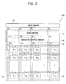
- FIG. 2 is a detailed block diagram of the OLED array shown in FIG. 1;
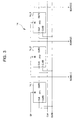
- FIG. 3 is a block diagram of a scan driver for the OLED array according to an exemplary embodiment of the present invention.
- FIG. 4A is a circuit diagram of an odd flip-flop according to an exemplary embodiment of the present invention.
- FIG. 4B is a circuit diagram of an even flip-flop according to an exemplary embodiment of the present invention.
- FIG. 5 is a timing diagram illustrating the operation of the scan driver shown in FIG. 3;
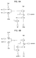
- FIG. 6A is a circuit diagram of an odd flip-flop according to an alternative exemplary embodiment of the present invention.
- FIG. 6B is a circuit diagram of an even flip-flop according to an alternative exemplary embodiment of the present invention.
- FIG. 1 is a block diagram of an organic light emitting display (OLED) device using a tiling technique.
- the OLED device is formed by bonding OLED arrays 100.
- OLED arrays 100 which are arranged four to a row and two to a column, are bonded to one another.
- the OLED device of the present invention may be designed to include a different number of OLED arrays 100 and to have various sizes.
- Each of the OLED arrays 100 includes an electroluminescent (EL) panel 10 for displaying a predetermined image, and a data driver 20 for supplying a data signal to the EL panel 10.
- EL electroluminescent
- the EL panels 10 have similar construction, and edges of the EL panels 10 are bonded to one another using an adhesive to form a combined EL panel.
- the adhesive may be an ultraviolet (UV) curing resin or a thermal curing resin, for example, epoxy resin.
- Each of the EL panels 10 can be produced by the same fabrication process as an EL panel for a conventional OLED array. Accordingly, a large combined EL panel can be fabricated by bonding EL panels that are obtained by the same fabrication process.
- Each of the EL panels 10 includes a scan driver, an emission control driver, and pixels, and each of the drivers and pixels includes a thin film transistor (TFT), which has a polysilicon channel in order to obtain fast response speed and high uniformity.
- TFT thin film transistor
- the polysilicon channel may be formed by forming an amorphous silicon (a-Si) layer on a glass substrate and crystallizing the a-Si layer using a low temperature polysilicon (LTPS) process.
- a-Si amorphous silicon
- LTPS low temperature polysilicon
- the TFTs are formed of polysilicon that is obtained using the LTPS process. Thereafter, the display region, the scan driver, and the emission control driver are formed using the transistors in each of the EL panels 10.
- the display region includes red (R), green (G), and blue (B) sub-pixels, and the scan and emission control drivers select respective pixels and generate signals for controlling an emission operation. A detailed description of the EL panel 10 will be presented later.
- Each of data drivers 20 is designed as an external integrated circuit (IC) using complementary metal oxide semiconductor (CMOS) technology and is electrically coupled to the corresponding EL panel 10.
- the EL panel 10 may be electrically coupled to the data driver 20 using a metal pattern that is printed on a flexible film. In that case, an output terminal of the data driver 20 is electrically coupled to one end of the metal pattern, and a data line located on the EL panel 10 is electrically coupled to the other end of the metal pattern. This method is referred to as a tape carrier package (TCP) technique.
- TCP tape carrier package
- Each of the data drivers 20 transmits a data signal to the display region of the EL panel 10 through conductive lines that are located on the flexible film.
- FIG. 2 is a detailed block diagram of the OLED array shown in FIG. 1.
- the OLED array 100 includes the EL panel 10 and the data driver 20.
- the EL panel 10 further includes a display region 12, a scan driver 14, and an emission control driver 16.
- the display region 12 includes data lines D1-Dm, scan lines S1-Sn, emission control lines E1-En, and pixels P11-Pnm that are formed in pixel regions 18.
- the data lines D1-Dm are electrically coupled to the data driver 20 and extend in a vertical direction of the exemplary embodiment shown in FIG. 2.
- the data lines D1-Dm transmit data signals to the respective pixels P11-Pnm.
- the data line D1 is coupled to pixels P11-Pn1
- the data line D2 is coupled to pixels P12-Pn2
- the data line Dm is coupled to pixels P1 m-Pnm.
- the scan lines S1-Sn and the emission control lines E1-En extend in the same direction as the data lines D1-Dm (i.e., in the vertical direction of the exemplary embodiment shown in FIG. 2).
- each of the scan and emission control lines S1-Sn and E1-En includes a contact hole in order to transmit the same scan and emission control signals to the pixels arranged in a horizontal direction of the exemplary embodiment of FIG. 2. Therefore, metal interconnections, which contact the scan and emission control lines S1-Sn and E1-En through the contact holes, extend in a horizontal direction so that scan and emission control signals are transmitted to the pixels arranged in the horizontal direction.
- the scan control signal from the scan line S1 and the emission control signal from the emission control line E1 are transmitted to the pixels P11-P1m
- the scan and emission control signals from S2 and E2 are transmitted to the pixels P21-P2m
- the scan and emission control signals from Sn and En are transmitted to the pixels Pn1-Pnm.
- Each of the pixels P11-Pnm includes R, G, and B sub-pixels that are repeatedly arranged in rows and columns.
- the pixels include an organic emission layer that emits light.
- the organic emission layers in the R, G, and B sub-pixels are formed of different organic materials, but are the same in interconnection layout or circuit connection of a driving circuit. Accordingly, each of the pixels P11-Pnm emits R, G, or B light at a luminance corresponding to a data signal applied to the pixel and combines the R, G, and B lights to display a specific color.
- the scan driver 14 is formed between the data driver 20 and the display region 12. Since a large panel is formed by bonding a number of EL panels 10 together, the scan driver 14 is formed on the same side as the data driver 20.
- the scan driver 14 is coupled to scan lines S1-Sn. Thus, the scan driver 14 sequentially transmits scan signals to the display region 12 and sequentially selects the pixels P11-Pnm.
- the emission control driver 16 is formed between the scan driver 14 and the display region 12 and is coupled to the emission control lines E1-En. Thus, the emission control driver 16 sequentially transmits emission control signals to the display region 12 and controls an emission time of each of the pixels P11-Pnm.
- the data driver 20 may transmit data signals to the display region 12 of the EL panel 10 through conductive lines located on the flexible film as described above.
- the OLED array 100 includes the EL panel 10 and the data driver 20, and the EL panel 10 includes the display region 12, the scan driver 14, and the emission control driver 16.
- the structure and operation of the scan driver 14 will be described in detail with reference to exemplary embodiments of the present invention.
- FIG. 3 is a block diagram of a scan driver for the OLED array according to an exemplary embodiment of the present invention.
- the scan driver 14 includes flip-flops FF1, FF2, FF3 ... FFn that are also labeled as a first flip-flop 14_1, a second flip-flop 14_2, a third filp-flop 14_3 and so on.
- the first flip-flop 14_1 receives a start pulse SP (e.g., a start signal) and outputs a first output signal OUT1 in synchronization with a clock signal CLK and an inverted clock signal CLKB.
- the first output signal OUT1 is shifted and input to a second flip-flop 14_2.
- the first output signal OUT1 becomes a first scan signal SCAN[1], which is used to select pixels located in a first row of pixels P11-P1 m of the display region 12 of FIG. 2.
- the second flip-flop 14_2 receives the first output signal OUT1 and outputs a second output signal OUT2 in synchronization with the clock signal CLK and the inverted clock signal CLKB that are shifted by a half cycle with respect to the first output signal OUT1.
- the second output signal OUT2 is input to a third flip-flop 14_3.
- the second output signal OUT2 becomes a second scan signal SCAN[2], which is used to select pixels located in a second row of pixels P21-P2m of the display region 12.
- the third flip-flop 14_3 receives the second output signal OUT2 and outputs a third output signal OUT3 in synchronization with the clock signal CLK and the inverted clock signal CLKB that are shifted by a half cycle of the clock signal CLK with respect to the second output signal OUT2.
- the third output signal OUT3 is input to a fourth flip-flop (not shown). Also, the third output signal OUT3 becomes a third scan signal that is used to select pixels located in a third row P31-P3m of the display region 12.
- the flip-flops 14_1, 14_2, 14_3 and so forth alternately receive the clock signal CLK and the inverted clock signal CLKB, and output scan signals SCAN including SCAN[1], SCAN[2], SCAN[3] and so forth, that are shifted by a half cycle of the clock signal CLK.
- a clock signal CLK input to an odd flip-flop 14_1 is input as an inverted clock signal CLKB to an even flip-flop 14_2, whereas the inverted clock signal CLKB input to the odd flip-flop 14_1 is input as a clock signal CLK to the even flip-flop 14_2.
- the scan signal SCAN can be output every half cycle of the clock signal CLK.
- the scan driver 14 includes three flip-flops 14_1, 14_2, and 14_3, but the present invention is not limited to this configuration. Rather, the scan driver 14 may include flip-flops in a number equal to the number of scan signals required (for example n in the case of the exemplary embodiment shown in FIG. 2).
- FIG. 4A is a circuit diagram of an odd flip-flop, for example 14_1, 14_3, and the like, according to an exemplary embodiment of the present invention.
- the first flip-flop 14_1 is shown in FIG. 4A as an example of odd flip-flops.
- the odd flip-flop includes three transistors M1, M2, and M3 and a capacitor C.
- the first transistor M1 is coupled between a positive power supply voltage line Vdd and a node N1, and a clock signal CLK is input to a gate terminal of the first transistor M1.
- the node N1 is the signal line for the scan signal being generated by the flip-flop.
- the second transistor M2 has a first electrode coupled to the node N1, and a gate terminal coupled to a node N2.
- the node N2 is the gate terminal of the second transistor M2.
- An inverted clock signal CLKB is input to a second electrode of the second transistor M2.
- the third transistor M3 has a first electrode coupled to the node N2.
- a start pulse SP is input to a second electrode of the third transistor M3, and the clock signal CLK is input to a gate terminal thereof.
- the inputs to the first flip-flop 14_1 are shown and therefore input to the second electrode of the third transistor M3 is shown as the start pulse SP which is the input to the first flip-flop 14_1.
- each of flip-flops 14_2, 14_3,... other than the first flip-flop 14_1 receives an output signal of the previous flip-flop as an input signal. So other odd flip-flops, such as 14_3, would receive other input signals, such as SCAN[2], at the second electrode of their third transistor M3.
- the first through third transistors M1, M2, and M3 are metal oxide semiconductor field effect transistors (MOSFETs) of the same conductivity type.
- MOSFETs metal oxide semiconductor field effect transistors
- FIG. 4A and FIG. 4B it will be described that the first through third M1, M2, and M3 are shown as p-type MOSFETs, but the present invention is not limited to this conductivity type.
- the capacitor C is coupled between the nodes N1 and N2 and maintains a voltage between the first electrode and the gate terminal of the second transistor M2.
- the capacitor C allows the flip-flop to be pulled down and generally leads the flip-flop to be in the same full-swing as a driving voltage.
- a high-level scan signal SCAN that is SCAN[1] in the exemplary case shown, is output through a scan line coupled to the node N1.
- a voltage difference between a source electrode and a drain electrode of the second transistor M2 becomes 0 V, thus static current is completely cut off from the second transistor M2.
- both the first and third transistors M1 and M3 are turned off.
- the second transistor M2 since the low-level inverted clock signal CLKB is applied to the second electrode of the second transistor M2, the second transistor M2 is turned on.
- a voltage at the node N1 is dropped as much as the low-level inverted clock signal CLKB.
- the third transistor M3 is turned off, the node N2 coupled to one terminal of the capacitor C is floated.
- a voltage at the node N2 is dropped as much as the voltage at the node N1 so that the voltage at the node N2 can be pulled down.
- a low-level scan signal SCAN[1] is output to a scan line coupled to the node N1.
- FIG. 4B is a circuit diagram of an even flip-flop, for example 14_2, 14_4, and the like, according to an exemplary embodiment of the present invention.
- the second flip-flop 14_2 is shown in FIG. 4B as an example of even flip-flops.
- the even flip-flop has the same construction as the odd flip-flop shown in FIG. 4A. That is, the even flip-flop includes three transistors M1, M2, and M3 and a capacitor C. For brevity of explanation, a description of the construction of the even flip-flop will be omitted here.
- a clock signal CLK and an inverted clock signal CLKB are input in inverse relation to the odd flip-flop.
- the output signal SCAN[1] of the previous odd flip-flop is input instead of the start pulse SP.
- the inverted clock signal CLKB is input to a gate terminal of the first transistor M1 and a gate terminal of the third transistor M3, and the clock signal CLK is input to a second electrode of the second transistor M2.
- the output signal SCAN[1] of the previous odd flip-flop is input to a second electrode of the third transistor M3.
- the above-described even flip-flop operates in the same manner as the odd flip-flop as described with reference to FIG. 4A and outputs a scan signal SCAN[2] in synchronization with a clock signal CLK that is shifted by a half clock cycle with respect to the inverted clock signal CLKB input to the previous flip flop.
- the scan driver of the present invention alternately inputs a clock signal CLK and an inverted clock signal CLKB to each of the flip-flops and outputs a scan signal that is shifted by a half clock cycle.
- each of the flip-flops includes the three transistors M1, M2, M3 and one capacitor C.
- layout area can be minimized owing to simplification of circuits.
- SCAN high-level scan signal
- the flow of static current is prevented due to a high-level signal that is applied to a drain terminal of the second transistor M2.
- power consumption can be reduced.
- the capacitor C is coupled between the source and gate of the second transistor M2, when a low-level scan signal SCAN is output, sufficient pull-down operation is enabled.
- FIG. 5 is a timing diagram illustrating the operation of the scan driver shown in FIG. 3.
- a low-level clock signal CLK, a high-level inverted clock signal CLKB, and a low-level start pulse SP are input.
- all the first, second, and third transistors M1, M2, and M3 are turned on.
- the node N1 outputs a high-level scan signal SCAN[1].
- the second transistor M2 is turned on, but a voltage between the source and drain of the second transistor M2 becomes 0V due to the high-level inverted clock signal CLKB applied to the second electrode of the second transistor M2, so that the flow of static current can be substantially cut off. As a result, power consumption caused by the static current is reduced.
- the clock signal CLK is shifted by a half clock cycle so that a high-level clock signal CLK, a low-level clock signal CLKB, and a high-level start pulse SP are input to the first flip-flop 14_1.
- both the first and third transistors M1 and M3 are turned off.
- one terminal of the capacitor C coupled to the node N2 is floated.
- the second transistor M2 is being turned on, current flows due to a voltage difference between the source and gate of the second transistor M2 and a voltage difference between the source and drain of this transistor. Accordingly, a voltage at the node N1 is dropped as much as the low-level inverted clock signal CLKB, thus the node N1 outputs a low-level scan signal SCAN[1].
- the clock signal CLK is shifted by a half clock cycle so that a low-level clock signal CLK, a high-level inverted clock signal CLKB, and a high-level start pulse SP are input to the first flip-flop 14_1.
- the second transistor M2 is turned off due to the high-level start pulse SP, and the node N1 outputs a high-level scan signal SCAN[1].
- the second flip-flop 14_2 receives the clock signal CLK that is shifted by a half clock cycle.
- a high-level clock signal CLK, a low-level inverted clock signal CLKB, and a low-level scan signal SCAN[1] are input to the second flip-flop 14_2.
- all the first, second, and third transistors M1, M2, and M3 are turned on.
- the node N1 outputs a high-level scan signal SCAN[2].
- the second transistor M2 is turned on, but a voltage between the source and drain of the second transistor M2 becomes 0V due to the high-level clock signal CLK applied to the second electrode of the second transistor M2, so that the flow of static current can be substantially cut off. As a result, power consumption caused by the static current is reduced.
- the clock signal CLK is shifted by a half clock cycle so that a low-level clock signal CLK, a high-level inverted clock signal CLKB, and a high-level scan signal SCAN[1] are input to the second flip-flop 14_2.
- both the first and third transistors M1 and M3 are turned off in response to the high-level inverted clock signal CLKB.
- one terminal of the capacitor C coupled to the node N2 is floated.
- the second transistor M2 is being turned on due to a voltage difference between the source and gate thereof, a voltage difference between the source and drain of the second transistor M2 arises from the low-level clock signal CLK, so that current flows. Accordingly, a voltage at the node N1 is dropped as much as the low-level clock signal CLK, thus the node N1 outputs a low-level scan signal SCAN[2].
- the clock signal CLK is shifted by a half clock cycle so that a high-level clock signal CLK, a low-level inverted clock signal CLKB, and a high-level scan signal SCAN[1] are input to the second flip-flop 14_2.
- the second transistor M2 is turned off due to the high-level scan signal SCAN[1], and the node N1 outputs a high-level scan signal SCAN[2].
- the remaining flip-flops 14_3, 14_4, and so forth perform the same operations as the first and second flip-flops 14_1 and 14_2 and output scan signals SCAN.
- the scan driver of the present invention makes use of three transistors and one capacitor and outputs the scan signal SCAN[n] every half cycle of the clock signal CLK.
- a clock signal CLK and an inverted clock signal CLKB are directly input to a gate terminal of a transistor.
- an output signal i.e., a scan signal SCAN
- a delay in the scan signal makes application of a data signal incorrect, thus an undesirable image may be displayed.
- FIG. 6A is a circuit diagram of an odd flip-flop according to an alternative exemplary embodiment of the present invention.
- the odd flip-flop has almost the same construction as the odd flip-flop shown in FIG. 4A. Thus, a description of the same components will be omitted here.
- a control signal input portion is coupled to gate terminals of a first transistor M1 and a third transistor M3.
- the control signal input portion includes two transistors M4 and M5.
- the fourth transistor M4 is coupled between a negative power supply voltage terminal Vss and the gate terminals of the first and third transistors M1 and M3, and a clock signal CLK is input to a gate terminal thereof.
- the fifth transistor M5 is coupled between a positive power supply voltage terminal Vdd and the gate terminals of the first and third transistors M1 and M3, and an inverted clock signal CLKB is input to a gate terminal of the fifth transistor M5.
- the fourth transistor M4 is turned on, so that the negative power supply voltage Vss is commonly applied to the gate terminals of the first and third transistors M1 and M3.
- the fifth transistor M5 is turned on, so that a positive power supply voltage Vdd is commonly applied to the gate terminals of the first and third transistors M1 and M3. Since the operating principle of the odd flip-flop of FIG. 6A is the same as the odd flip-flop of FIG. 4A, a description thereof will be omitted here.
- FIG. 6B is a circuit diagram of an even flip-flop according to an alternative exemplary embodiment of the present invention.
- the alternative even flip-flop has the same construction as the odd flip-flop shown in FIG. 6A.
- a clock signal CLK and an inverted clock signal CLKB are input in inverse relation to the odd flip-flop shown in FIG. 6A.
- the inverted clock signal CLKB is input to a terminal to which the clock signal CLK is input in the odd flip-flop of FIG. 6A, while the clock signal CLK is input to a terminal to which the inverted clock signal CLKB is input in the odd flip-flop of FIG. 6A. Since the operations of the even flip-flop of FIG. 6B are the same as that of the even flip-flop of FIG. 4B, a description thereof will not be repeated here.
- each of the flip-flops since each of the flip-flops includes the three transistors M1, M2, and M3 and a capacitor C, layout area can be minimized due to simplification of circuits. Also, when a high-level scan signal SCAN is output, the flow of static current is prevented due to a high-level signal that is applied to a drain terminal of the second transistor M2. As a result, power consumption can be reduced. Furthermore, since the capacitor C is coupled between a source terminal and a gate terminal of the second transistor M2, when a low-level scan signal SCAN is output, a sufficient pull-down operation is enabled. In addition, each of the odd and even flip-flops of the alternative embodiment, includes the control signal input portion unlike the first embodiment, with the result that a delay in an output signal caused by a delay in the clock signal CLK can be prevented.
- a display panel includes flip-flops, each of which is comprised of three transistors and a capacitor, so that layout area is minimized with simplification of circuits while facilitating construction of an SOP-type display panel.
- a low-level scan signal can be output in the same waveform as a driving voltage so that a sufficient pull-down operation is enabled.
- the present invention provides not only a simplified SOP-type scan driver but also an OLED device that can minimize power consumption.
Landscapes
- Engineering & Computer Science (AREA)
- Physics & Mathematics (AREA)
- Computer Hardware Design (AREA)
- General Physics & Mathematics (AREA)
- Theoretical Computer Science (AREA)
- Control Of Indicators Other Than Cathode Ray Tubes (AREA)
- Electroluminescent Light Sources (AREA)
- Shift Register Type Memory (AREA)
- Control Of El Displays (AREA)
Abstract
Description
- The present invention relates to an organic light emitting display (OLED) device and, more particularly, to a system on panel (SOP) type scan driver which generates scan signals for selecting pixels located on a display region, and an OLED device having the same.
- Recent years have seen considerable research into flat panel displays (FPDs) because they can be made smaller and lighter than display devices using cathode ray tubes (CRTs). As a result, liquid crystal displays (LCDs), field emission displays (FEDs), plasma display panels (PDPs), and organic light emitting displays (OLEDs) have been developed and put to practical use. Among these FPDs, the PDP can have a large screen but has low luminance and poor luminous efficiency resulting in high power consumption, and the LCD has a relatively slow response speed and consumes a lot of power since it employs a backlight.
- However, as the OLED makes use of an organic material to emit light, it has a wider viewing angle and faster response speed than the LCD. Also, the OLED is an emissive display that obtains good contrast and visibility. Further, the OLED enables lower power consumption and can be made thin and lightweight because it needs no backlight.
- Nevertheless, the dimensions of an electroluminescent (EL) panel for a glass substrate are limited due to fabricating process limitations and the OLED may not be easily constructed to have a large screen. Also, if the screen is large, there is a greater probability of a defect occurring somewhere on the screen and thus a reduction in yield is unavoidable. Further, it is difficult to obtain uniformity across the screen.
- As a solution to the above problems of the OLED, a tiling technique was developed. In the tiling technique, EL panels are bonded together like tiles to form a single panel.
- Each of the EL panels includes pixels to display a predetermined image similar to a conventional OLED. In each of the EL panels, a scan driver applies a scan signal to enable the pixels, and a data driver applies a data signal to a selected pixel. Also, an emission control driver applies an emission control signal to each of the pixels in order to control the exact programming of the data signal and the time taken for an emission operation.
- As described above, the scan driver, the data driver, and the emission control driver, which transmit various signals to drive the EL panels, can be electrically coupled to each of the EL panels in various manners.
- For example, the scan driver, the data driver, and the emission control driver may be mounted as chips on a tape carrier package (TCP) that is bonded and electrically coupled to each of the EL panels. Alternatively, the drivers may be mounted as chips on a flexible printed circuit (FPC) or a film that is bonded and electrically coupled to each of the EL panels. The latter technique is referred to as a chip on flexible board (or chip on film) (COF) technique. In another method, the drivers are directly mounted on a glass substrate of the EL panel. This method is referred to as a chip on glass (COG) technique. These methods are costly and only complicate the modules, because the drivers should be separately designed and electrically coupled to one another.
- To overcome these drawbacks, a system on panel (SOP) technique has been developed recently. Also, there have been attempts at designing a display region, scan and emission control drivers, and/or a data driver in each EL panel, in order to include all parts of the system in each of the EL panels.
- In the OLED using the tiling technique, when each EL panel is formed as an SOP, it is easy to bond the EL panels to one another. Also, the SOP technique enables the area of drivers to be reduced and cost and labor for designing integrated circuits (ICs) of the respective drivers to be saved.
- However, in order to develop the SOP-type OLED, it is necessary to consider many internal circumstances and conditions of the EL panels, such as a driving frequency and electron mobility of the data driver and/or the scan and emission control drivers. Up to present, it has been difficult to design the data driver within a panel because the data driver needs a high driving frequency.
- Accordingly, the data driver is formed separately as an IC using complementary metal oxide semiconductor (CMOS) technology and subsequently coupled to the EL panel, while the scan driver and/or the emission control driver are formed within the EL panel.
- Therefore, there is a need for a simple circuit construction in which an SOP-type scan driver and emission control driver can be optimally driven in the EL panel.
- The present invention, therefore, provides a scan driver for an organic light emitting display (OLED) device, which is designed as a system on panel (SOP) type in an electroluminescent (EL) panel and generates scan signals for selecting pixels.
- In an exemplary embodiment of the present invention, an OLED device includes a display region having pixels and displaying a predetermined image, a scan driver having flip-flops and applying a scan signal to sequentially select the pixels, a data driver applying a data signal to the pixels that are selected by the scan signal, and an emission control driver applying an emission control signal to control an emission operation of the pixels, wherein each of the flip-flops of the scan driver includes a first transistor, coupled between a positive power supply voltage terminal and a first node, and turned on/off according to a control signal applied to a gate terminal of the first transistor, a second transistor, coupled between the first node and an inverted control signal line and turned on/off according to a voltage at a second node coupled to a gate terminal of the second transistor, and a third transistor having a first electrode and a second electrode, wherein the first electrode of the third transistor is coupled to the second node and an input signal applied to the second electrode of the third transistor is transmitted to the first electrode of the third transistor according to the control signal applied to a gate terminal of the third transistor.
In other words, an organic light emitting display device comprises a display region having pixels for displaying a predetermined image; a scan driver having flip-flops and applying a scan signal to select the pixels; a data driver for applying a data signal to selected pixels; and an emission control driver for applying an emission control signal to control an emission operation of the pixels, wherein at least one of the flip-flops of the scan driver includes: - a first transistor, coupled between a positive power supply voltage terminal and a signal line for the scan signal, and turned on/off according to a control signal applied to a gate terminal of the first transistor;
- a second transistor, coupled between the signal line for the scan signal and a signal line for an inverted control signal and turned on/off according to a voltage at a gate terminal of the second transistor; and
- a third transistor having a first electrode and a second electrode,
- wherein the first electrode of the third transistor is coupled to the gate terminal of the second transistor and an input signal applied to the second electrode of the third transistor is transmitted to the first electrode of the third transistor according to the control signal applied to a gate terminal of the third transistor.
- In another exemplary embodiment of the present invention, an OLED device includes a display region having pixels and displaying a predetermined image, a scan driver having flip-flops and applying a scan signal to sequentially select the pixels, a data driver applying a data signal to the pixels that are selected by the scan signal, and an emission control driver applying an emission control signal to control an emission operation of the pixels, wherein each of the flip-flops of the scan driver includes a first transistor, coupled between a positive power supply voltage terminal and a first node, and turned on/off according to a control signal applied to a gate terminal of the first transistor, a second transistor, coupled between the first node and one of a clock signal line and an inverted clock signal line and turned on/off according to a voltage at the second node coupled to a gate terminal of the second transistor, a third transistor having a first electrode and a second electrode, wherein the first electrode of the third transistor is coupled to a second node and an input signal applied to the second electrode of the third transistor is transmitted to the first electrode of the third transistor according to the control signal applied to a gate terminal of the third transistor, and a control signal input portion, commonly coupled to the gate terminals of the first and third transistors and applying the control signal of a low or high level in response to one of the clock signal and the inverted clock signal.
In other words, an organic light emitting display device comprises a display region having pixels for displaying a predetermined image; a scan driver having flip-flops for applying a scan signal to select the pixels; a data driver for applying a data signal to selected pixels; and an emission control driver for applying an emission control signal for controlling an emission operation of the pixels, wherein at least one of the flip-flops of the scan driver includes: - a first transistor, coupled between a positive power supply voltage terminal and a signal line for scan signals, and turned on/off according to a control signal applied to a gate terminal of the first transistor;
- a second transistor, coupled between the signal line for the scan signal and either a signal line for a clock signal or a signal line for an inverted clock signal and turned on/off according to a voltage at a gate terminal of the second transistor;
- a third transistor having a first electrode and a second electrode,
- wherein the first electrode of the third transistor is coupled to the gate of the second transistor and an input signal applied to the second electrode of the third transistor is transmitted to the first electrode of the third transistor according to the control signal applied to a gate terminal of the third transistor; and a control signal input portion, commonly coupled to the gate terminal of the first transistor and the gate terminal of the third transistor and applying the control signal of a low or high level in response to either a clock signal or an inverted clock signal.
- The control signal input portion may include a fourth transistor, coupled between a negative power supply voltage terminal and the gate terminal of the first transistor and the gate terminal of the third transistor, and turned on/off in response to either the clock signal or the inverted clock signal, and a fifth transistor, coupled between a positive power supply voltage terminal and the gate terminal of the first transistor and the gate terminal of the third transistor, and turned on/off in response to either the inverted clock signal or the clock signal.
Preferably, the clock signal and the inverted clock signal are alternately input to an odd flip-flop and an even flip-flop.
Preferably, the at least one of the flip-flops is for outputting a scan signal via the signal line for the scan signal and for inputting the scan signal to the next flip-flop.
Preferably, the at least one of the flip-flops is for outputting the scan signal every half cycle of the clock signal.
Preferably, the first transistor, the second transistor, the third transistor, the fourth transistor, and the fifth transistor are PMOS transistors. - Another exemplary embodiment presents an organic light emitting display device including a data driver for generating data signals corresponding to an image to be displayed by the device, and an electroluminescent panel coupled to the data driver. The electroluminescent panel may include a scan driver for generating scan signals. The scan driver may have flip-flops coupled together, a first flip-flop for receiving a clock signal as a control signal and a start pulse as an input signal and generating a first scan signal, a second flip-flop for receiving an inverted clock signal as a control signal and the first scan signal as an input signal and generating a second scan signal, the second scan signal being shifted by half cycle of the clock signal with respect to the first scan signal, an emission control driver for generating emission control signals, and a display region. The display region may include pixels coupled to the data driver, the scan driver and the emission control driver, for receiving the data signals, the scan signals and the emission control signals, the pixels being controlled by the scan signals and the emission control signals, the pixels for generating light according to the data signals. Each of the flip-flops may include three transistors of a first conductivity type and a capacitor. Each of the flip-flops may further include a control signal input portion having two transistors also of the first conductivity type, and each of the flip-flops may receive the clock signal or the inverted clock signal at the control signal input portion.
- In another embodiment, a method for generating scan signals for driving an organic light emitting display device is presented. The device may include a scan driver comprised of flip-flops coupled together in series, a first one of the flip-flops receiving a start pulse as input and each of the flip-flops after the first flip-flop receiving an output signal of a previous one of the flip-flops as input, and the output signal of each one of the flip-flops being one of the scan signals. The method includes providing a clock signal having a low level during a first half clock cycle to the first one of the flip-flops, providing the start pulse having the low level during the first half clock cycle to the first one of the flip-flops, generating a first one of the scan signals by the first one of the flip-flops, the first one of the scan signals having a high level during the first half clock cycle and the low level during a second half clock cycle, providing an inverted clock signal having the low level during a second half clock cycle to a second one of the flip-flops coupled to the first one of the flip-flops, providing the first one of the scan signals to the second one of the flip-flops, and generating a second one of the scan signals by the second one of the flip-flops, the second one of the scan signals having the high level during the first half clock cycle and the second half clock cycle and the low level during a third half clock cycle.
- The flip-flops include transistors of only a first conductivity type. Each of the flip-flops may further include a control signal input portion having transistors of the first conductivity type. The method may also include providing the clock signal to the first one of the flip-flops through the control signal input portion of the first one of the flip-flops and providing the inverted clock signal to the second one of the flip-flops through the control signal input portion of the second one of the flip-flops.
Preferably, the providing of the clock signal includes controlling a coupling of a negative power supply to the first one of the flip-flops, and the providing of the inverted clock signal includes controlling a coupling of a positive power supply to the second one of the flip-flops.
Preferably, the method further comprises providing the inverted clock signal to the first one of the flip-flops for preventing static current through the first one of the flip flops; and providing the clock signal to the second one of the flip-flops for preventing static current through the second one of the flip flops.
Preferably, the method further comprises providing storage capacitance in the flip-flops for sufficient pull-down. - The above and other features of the present invention will be described in reference to certain exemplary embodiments thereof with reference to the attached drawings in which:
- FIG. 1 is a block diagram of an organic light emitting display (OLED) device using a tiling technique;
- FIG. 2 is a detailed block diagram of the OLED array shown in FIG. 1;
- FIG. 3 is a block diagram of a scan driver for the OLED array according to an exemplary embodiment of the present invention;
- FIG. 4A is a circuit diagram of an odd flip-flop according to an exemplary embodiment of the present invention;
- FIG. 4B is a circuit diagram of an even flip-flop according to an exemplary embodiment of the present invention;
- FIG. 5 is a timing diagram illustrating the operation of the scan driver shown in FIG. 3;
- FIG. 6A is a circuit diagram of an odd flip-flop according to an alternative exemplary embodiment of the present invention; and
- FIG. 6B is a circuit diagram of an even flip-flop according to an alternative exemplary embodiment of the present invention.
- The present invention will now be described more fully hereinafter with reference to the accompanying drawings, in which exemplary embodiments of the invention are shown.
- FIG. 1 is a block diagram of an organic light emitting display (OLED) device using a tiling technique.
- Referring to FIG. 1, the OLED device is formed by
bonding OLED arrays 100. In FIG. 1, it is illustrated that eightOLED arrays 100, which are arranged four to a row and two to a column, are bonded to one another. However, the OLED device of the present invention may be designed to include a different number ofOLED arrays 100 and to have various sizes. - Each of the
OLED arrays 100 includes an electroluminescent (EL)panel 10 for displaying a predetermined image, and adata driver 20 for supplying a data signal to theEL panel 10. - The
EL panels 10 have similar construction, and edges of theEL panels 10 are bonded to one another using an adhesive to form a combined EL panel. The adhesive may be an ultraviolet (UV) curing resin or a thermal curing resin, for example, epoxy resin. - Each of the
EL panels 10 can be produced by the same fabrication process as an EL panel for a conventional OLED array. Accordingly, a large combined EL panel can be fabricated by bonding EL panels that are obtained by the same fabrication process. - Each of the
EL panels 10 includes a scan driver, an emission control driver, and pixels, and each of the drivers and pixels includes a thin film transistor (TFT), which has a polysilicon channel in order to obtain fast response speed and high uniformity. In this case, the polysilicon channel may be formed by forming an amorphous silicon (a-Si) layer on a glass substrate and crystallizing the a-Si layer using a low temperature polysilicon (LTPS) process. - The TFTs are formed of polysilicon that is obtained using the LTPS process. Thereafter, the display region, the scan driver, and the emission control driver are formed using the transistors in each of the
EL panels 10. The display region includes red (R), green (G), and blue (B) sub-pixels, and the scan and emission control drivers select respective pixels and generate signals for controlling an emission operation. A detailed description of theEL panel 10 will be presented later. - Each of
data drivers 20 is designed as an external integrated circuit (IC) using complementary metal oxide semiconductor (CMOS) technology and is electrically coupled to thecorresponding EL panel 10. TheEL panel 10 may be electrically coupled to thedata driver 20 using a metal pattern that is printed on a flexible film. In that case, an output terminal of thedata driver 20 is electrically coupled to one end of the metal pattern, and a data line located on theEL panel 10 is electrically coupled to the other end of the metal pattern. This method is referred to as a tape carrier package (TCP) technique. Each of thedata drivers 20 transmits a data signal to the display region of theEL panel 10 through conductive lines that are located on the flexible film. - FIG. 2 is a detailed block diagram of the OLED array shown in FIG. 1.
- Referring to FIG. 2, the
OLED array 100 includes theEL panel 10 and thedata driver 20. TheEL panel 10 further includes adisplay region 12, ascan driver 14, and anemission control driver 16. - The
display region 12 includes data lines D1-Dm, scan lines S1-Sn, emission control lines E1-En, and pixels P11-Pnm that are formed inpixel regions 18. - The data lines D1-Dm are electrically coupled to the
data driver 20 and extend in a vertical direction of the exemplary embodiment shown in FIG. 2. The data lines D1-Dm transmit data signals to the respective pixels P11-Pnm. For example, the data line D1 is coupled to pixels P11-Pn1, the data line D2 is coupled to pixels P12-Pn2, and the data line Dm is coupled to pixels P1 m-Pnm. - Unlike in a conventional OLED device, the scan lines S1-Sn and the emission control lines E1-En extend in the same direction as the data lines D1-Dm (i.e., in the vertical direction of the exemplary embodiment shown in FIG. 2). However, each of the scan and emission control lines S1-Sn and E1-En includes a contact hole in order to transmit the same scan and emission control signals to the pixels arranged in a horizontal direction of the exemplary embodiment of FIG. 2. Therefore, metal interconnections, which contact the scan and emission control lines S1-Sn and E1-En through the contact holes, extend in a horizontal direction so that scan and emission control signals are transmitted to the pixels arranged in the horizontal direction. For example, the scan control signal from the scan line S1 and the emission control signal from the emission control line E1 are transmitted to the pixels P11-P1m, the scan and emission control signals from S2 and E2 are transmitted to the pixels P21-P2m, and the scan and emission control signals from Sn and En are transmitted to the pixels Pn1-Pnm.
- Each of the pixels P11-Pnm includes R, G, and B sub-pixels that are repeatedly arranged in rows and columns. The pixels include an organic emission layer that emits light. The organic emission layers in the R, G, and B sub-pixels are formed of different organic materials, but are the same in interconnection layout or circuit connection of a driving circuit. Accordingly, each of the pixels P11-Pnm emits R, G, or B light at a luminance corresponding to a data signal applied to the pixel and combines the R, G, and B lights to display a specific color.
- In the exemplary embodiment of FIG. 2, the
scan driver 14 is formed between thedata driver 20 and thedisplay region 12. Since a large panel is formed by bonding a number ofEL panels 10 together, thescan driver 14 is formed on the same side as thedata driver 20. Thescan driver 14 is coupled to scan lines S1-Sn. Thus, thescan driver 14 sequentially transmits scan signals to thedisplay region 12 and sequentially selects the pixels P11-Pnm. - In the exemplary embodiment shown, the
emission control driver 16 is formed between thescan driver 14 and thedisplay region 12 and is coupled to the emission control lines E1-En. Thus, theemission control driver 16 sequentially transmits emission control signals to thedisplay region 12 and controls an emission time of each of the pixels P11-Pnm. - The
data driver 20 may transmit data signals to thedisplay region 12 of theEL panel 10 through conductive lines located on the flexible film as described above. - According to the embodiments described above, the
OLED array 100 includes theEL panel 10 and thedata driver 20, and theEL panel 10 includes thedisplay region 12, thescan driver 14, and theemission control driver 16. Hereinafter, the structure and operation of thescan driver 14 will be described in detail with reference to exemplary embodiments of the present invention. - FIG. 3 is a block diagram of a scan driver for the OLED array according to an exemplary embodiment of the present invention.
- Referring to FIG. 3, the
scan driver 14 includes flip-flops FF1, FF2, FF3 ... FFn that are also labeled as a first flip-flop 14_1, a second flip-flop 14_2, a third filp-flop 14_3 and so on. The first flip-flop 14_1 receives a start pulse SP (e.g., a start signal) and outputs a first output signal OUT1 in synchronization with a clock signal CLK and an inverted clock signal CLKB. The first output signal OUT1 is shifted and input to a second flip-flop 14_2. Also, the first output signal OUT1 becomes a first scan signal SCAN[1], which is used to select pixels located in a first row of pixels P11-P1 m of thedisplay region 12 of FIG. 2. - The second flip-flop 14_2 receives the first output signal OUT1 and outputs a second output signal OUT2 in synchronization with the clock signal CLK and the inverted clock signal CLKB that are shifted by a half cycle with respect to the first output signal OUT1. The second output signal OUT2 is input to a third flip-flop 14_3. Also, the second output signal OUT2 becomes a second scan signal SCAN[2], which is used to select pixels located in a second row of pixels P21-P2m of the
display region 12. - The third flip-flop 14_3 receives the second output signal OUT2 and outputs a third output signal OUT3 in synchronization with the clock signal CLK and the inverted clock signal CLKB that are shifted by a half cycle of the clock signal CLK with respect to the second output signal OUT2. The third output signal OUT3 is input to a fourth flip-flop (not shown). Also, the third output signal OUT3 becomes a third scan signal that is used to select pixels located in a third row P31-P3m of the
display region 12. - The flip-flops 14_1, 14_2, 14_3 and so forth alternately receive the clock signal CLK and the inverted clock signal CLKB, and output scan signals SCAN including SCAN[1], SCAN[2], SCAN[3] and so forth, that are shifted by a half cycle of the clock signal CLK. For example, a clock signal CLK input to an odd flip-flop 14_1 is input as an inverted clock signal CLKB to an even flip-flop 14_2, whereas the inverted clock signal CLKB input to the odd flip-flop 14_1 is input as a clock signal CLK to the even flip-flop 14_2. Thus, the scan signal SCAN can be output every half cycle of the clock signal CLK.
- It is illustrated in FIG. 3 that the
scan driver 14 includes three flip-flops 14_1, 14_2, and 14_3, but the present invention is not limited to this configuration. Rather, thescan driver 14 may include flip-flops in a number equal to the number of scan signals required (for example n in the case of the exemplary embodiment shown in FIG. 2). - FIG. 4A is a circuit diagram of an odd flip-flop, for example 14_1, 14_3, and the like, according to an exemplary embodiment of the present invention. The first flip-flop 14_1 is shown in FIG. 4A as an example of odd flip-flops.
- Referring to FIG. 4A, the odd flip-flop includes three transistors M1, M2, and M3 and a capacitor C.
- The first transistor M1 is coupled between a positive power supply voltage line Vdd and a node N1, and a clock signal CLK is input to a gate terminal of the first transistor M1. The node N1 is the signal line for the scan signal being generated by the flip-flop.
- The second transistor M2 has a first electrode coupled to the node N1, and a gate terminal coupled to a node N2. The node N2 is the gate terminal of the second transistor M2. An inverted clock signal CLKB is input to a second electrode of the second transistor M2.
- The third transistor M3 has a first electrode coupled to the node N2. A start pulse SP is input to a second electrode of the third transistor M3, and the clock signal CLK is input to a gate terminal thereof. In FIG. 4A, the inputs to the first flip-flop 14_1 are shown and therefore input to the second electrode of the third transistor M3 is shown as the start pulse SP which is the input to the first flip-flop 14_1. As described with reference to FIG. 3, each of flip-flops 14_2, 14_3,... other than the first flip-flop 14_1 receives an output signal of the previous flip-flop as an input signal. So other odd flip-flops, such as 14_3, would receive other input signals, such as SCAN[2], at the second electrode of their third transistor M3.
- The first through third transistors M1, M2, and M3 are metal oxide semiconductor field effect transistors (MOSFETs) of the same conductivity type. In FIG. 4A and FIG. 4B, it will be described that the first through third M1, M2, and M3 are shown as p-type MOSFETs, but the present invention is not limited to this conductivity type.
- The capacitor C is coupled between the nodes N1 and N2 and maintains a voltage between the first electrode and the gate terminal of the second transistor M2. The capacitor C allows the flip-flop to be pulled down and generally leads the flip-flop to be in the same full-swing as a driving voltage.
- For example, when the clock signal CLK is at a low level, the inverted clock signal CLKB is at a high level, and the start pulse SP is at a low level, both the first and third transistors M1 and M3 are turned on. Thus, a low-level start pulse SP is input to the gate terminal of the second transistor M2, so that the second transistor M2 is also turned on. However, because the high-level inverted clock signal CLKB is applied to the second electrode of the second transistor M2, no current flows through the second transistor M2. Thus, a high-level scan signal SCAN, that is SCAN[1] in the exemplary case shown, is output through a scan line coupled to the node N1. In this case, since the inverted clock signal CLKB is elevated to a high level, a voltage difference between a source electrode and a drain electrode of the second transistor M2 becomes 0 V, thus static current is completely cut off from the second transistor M2.
- Next, when the clock signal CLK is at a high level, the inverted clock signal CLKB is at a low level, and the start pulse SP is at a high level, both the first and third transistors M1 and M3 are turned off. In this case, since the low-level inverted clock signal CLKB is applied to the second electrode of the second transistor M2, the second transistor M2 is turned on. As current flows through the second transistor M2 due to a high-level voltage stored in the node N1, a voltage at the node N1 is dropped as much as the low-level inverted clock signal CLKB. Specifically, as the third transistor M3 is turned off, the node N2 coupled to one terminal of the capacitor C is floated. Thus, a voltage at the node N2 is dropped as much as the voltage at the node N1 so that the voltage at the node N2 can be pulled down. As a result, a low-level scan signal SCAN[1] is output to a scan line coupled to the node N1.
- FIG. 4B is a circuit diagram of an even flip-flop, for example 14_2, 14_4, and the like, according to an exemplary embodiment of the present invention. The second flip-flop 14_2 is shown in FIG. 4B as an example of even flip-flops.
- Referring to FIG. 4B, the even flip-flop has the same construction as the odd flip-flop shown in FIG. 4A. That is, the even flip-flop includes three transistors M1, M2, and M3 and a capacitor C. For brevity of explanation, a description of the construction of the even flip-flop will be omitted here.
- However, a clock signal CLK and an inverted clock signal CLKB are input in inverse relation to the odd flip-flop. Also, the output signal SCAN[1] of the previous odd flip-flop is input instead of the start pulse SP. Specifically, the inverted clock signal CLKB is input to a gate terminal of the first transistor M1 and a gate terminal of the third transistor M3, and the clock signal CLK is input to a second electrode of the second transistor M2. Also, the output signal SCAN[1] of the previous odd flip-flop is input to a second electrode of the third transistor M3.
- The above-described even flip-flop operates in the same manner as the odd flip-flop as described with reference to FIG. 4A and outputs a scan signal SCAN[2] in synchronization with a clock signal CLK that is shifted by a half clock cycle with respect to the inverted clock signal CLKB input to the previous flip flop.
- As described above, the scan driver of the present invention alternately inputs a clock signal CLK and an inverted clock signal CLKB to each of the flip-flops and outputs a scan signal that is shifted by a half clock cycle.
- In the embodiment of the present invention, each of the flip-flops includes the three transistors M1, M2, M3 and one capacitor C. Thus, layout area can be minimized owing to simplification of circuits. Also, when a high-level scan signal SCAN is output, the flow of static current is prevented due to a high-level signal that is applied to a drain terminal of the second transistor M2. As a result, power consumption can be reduced. Furthermore, since the capacitor C is coupled between the source and gate of the second transistor M2, when a low-level scan signal SCAN is output, sufficient pull-down operation is enabled.
- Hereinafter, the operation of the scan driver including flip-flops will be described with reference to FIG. 5.
- FIG. 5 is a timing diagram illustrating the operation of the scan driver shown in FIG. 3.
- First, the operation of the first flip-flop 14_1 that is a representative odd flip-flop will be described with reference to FIGs. 3, 4A, 4B, and 5.
- Referring to FIGs. 3 through 5, a low-level clock signal CLK, a high-level inverted clock signal CLKB, and a low-level start pulse SP are input. In this case, all the first, second, and third transistors M1, M2, and M3 are turned on. Thus, the node N1 outputs a high-level scan signal SCAN[1]. Here, the second transistor M2 is turned on, but a voltage between the source and drain of the second transistor M2 becomes 0V due to the high-level inverted clock signal CLKB applied to the second electrode of the second transistor M2, so that the flow of static current can be substantially cut off. As a result, power consumption caused by the static current is reduced.
- Thereafter, the clock signal CLK is shifted by a half clock cycle so that a high-level clock signal CLK, a low-level clock signal CLKB, and a high-level start pulse SP are input to the first flip-flop 14_1. Thus, both the first and third transistors M1 and M3 are turned off. In this case, one terminal of the capacitor C coupled to the node N2 is floated. While the second transistor M2 is being turned on, current flows due to a voltage difference between the source and gate of the second transistor M2 and a voltage difference between the source and drain of this transistor. Accordingly, a voltage at the node N1 is dropped as much as the low-level inverted clock signal CLKB, thus the node N1 outputs a low-level scan signal SCAN[1].
- Thereafter, the clock signal CLK is shifted by a half clock cycle so that a low-level clock signal CLK, a high-level inverted clock signal CLKB, and a high-level start pulse SP are input to the first flip-flop 14_1. In this case, the second transistor M2 is turned off due to the high-level start pulse SP, and the node N1 outputs a high-level scan signal SCAN[1].
- From the next cycle, although the clock signal CLK and the inverted clock signal CLKB make an upward or downward transition, since the start pulse SP is fixed at a high level, the node N1 always remains at a high level.
- Next, the operation of the second flip-flop 14_2 that is a representative even flip-flop will be described. The second flip-flop 14_2 receives the clock signal CLK that is shifted by a half clock cycle.
- Specifically, a high-level clock signal CLK, a low-level inverted clock signal CLKB, and a low-level scan signal SCAN[1] are input to the second flip-flop 14_2. In this case, all the first, second, and third transistors M1, M2, and M3 are turned on. Thus, the node N1 outputs a high-level scan signal SCAN[2]. Here, the second transistor M2 is turned on, but a voltage between the source and drain of the second transistor M2 becomes 0V due to the high-level clock signal CLK applied to the second electrode of the second transistor M2, so that the flow of static current can be substantially cut off. As a result, power consumption caused by the static current is reduced.
- Thereafter, the clock signal CLK is shifted by a half clock cycle so that a low-level clock signal CLK, a high-level inverted clock signal CLKB, and a high-level scan signal SCAN[1] are input to the second flip-flop 14_2. Thus, both the first and third transistors M1 and M3 are turned off in response to the high-level inverted clock signal CLKB. In this case, one terminal of the capacitor C coupled to the node N2 is floated. While the second transistor M2 is being turned on due to a voltage difference between the source and gate thereof, a voltage difference between the source and drain of the second transistor M2 arises from the low-level clock signal CLK, so that current flows. Accordingly, a voltage at the node N1 is dropped as much as the low-level clock signal CLK, thus the node N1 outputs a low-level scan signal SCAN[2].
- Thereafter, the clock signal CLK is shifted by a half clock cycle so that a high-level clock signal CLK, a low-level inverted clock signal CLKB, and a high-level scan signal SCAN[1] are input to the second flip-flop 14_2. In this case, the second transistor M2 is turned off due to the high-level scan signal SCAN[1], and the node N1 outputs a high-level scan signal SCAN[2].
- From now on, although the clock signal CLK and the inverted clock signal CLKB make an upward or downward transition every half cycle, since the scan signal SCAN[1] is fixed at a high level, the node N1 always remains at a high level.
- Subsequently, the remaining flip-flops 14_3, 14_4, and so forth, perform the same operations as the first and second flip-flops 14_1 and 14_2 and output scan signals SCAN.
- As described above, the scan driver of the present invention makes use of three transistors and one capacitor and outputs the scan signal SCAN[n] every half cycle of the clock signal CLK.
- In FIGS. 4A and 4B, a clock signal CLK and an inverted clock signal CLKB are directly input to a gate terminal of a transistor. Thus, when the clock signal CLK is delayed due to a line load, an output signal (i.e., a scan signal SCAN) also may be delayed. In particular, when the transistor has a large size, a delay in the scan signal makes application of a data signal incorrect, thus an undesirable image may be displayed.
- FIG. 6A is a circuit diagram of an odd flip-flop according to an alternative exemplary embodiment of the present invention.
- Referring to FIG. 6A, the odd flip-flop has almost the same construction as the odd flip-flop shown in FIG. 4A. Thus, a description of the same components will be omitted here.
- Referring to FIG. 6A, a control signal input portion is coupled to gate terminals of a first transistor M1 and a third transistor M3. The control signal input portion includes two transistors M4 and M5. The fourth transistor M4 is coupled between a negative power supply voltage terminal Vss and the gate terminals of the first and third transistors M1 and M3, and a clock signal CLK is input to a gate terminal thereof. The fifth transistor M5 is coupled between a positive power supply voltage terminal Vdd and the gate terminals of the first and third transistors M1 and M3, and an inverted clock signal CLKB is input to a gate terminal of the fifth transistor M5.
- Accordingly, once a low-level clock signal CLK is input, the fourth transistor M4 is turned on, so that the negative power supply voltage Vss is commonly applied to the gate terminals of the first and third transistors M1 and M3. Also, once a low-level inverted clock signal CLKB is input, the fifth transistor M5 is turned on, so that a positive power supply voltage Vdd is commonly applied to the gate terminals of the first and third transistors M1 and M3. Since the operating principle of the odd flip-flop of FIG. 6A is the same as the odd flip-flop of FIG. 4A, a description thereof will be omitted here.
- FIG. 6B is a circuit diagram of an even flip-flop according to an alternative exemplary embodiment of the present invention.
- Referring to FIG. 6B, the alternative even flip-flop has the same construction as the odd flip-flop shown in FIG. 6A. However, a clock signal CLK and an inverted clock signal CLKB are input in inverse relation to the odd flip-flop shown in FIG. 6A. Accordingly, in the even flip-flop of FIG. 6B, the inverted clock signal CLKB is input to a terminal to which the clock signal CLK is input in the odd flip-flop of FIG. 6A, while the clock signal CLK is input to a terminal to which the inverted clock signal CLKB is input in the odd flip-flop of FIG. 6A. Since the operations of the even flip-flop of FIG. 6B are the same as that of the even flip-flop of FIG. 4B, a description thereof will not be repeated here.
- In the alternative embodiment of the present invention, shown in FIGs. 6A and 6B, since each of the flip-flops includes the three transistors M1, M2, and M3 and a capacitor C, layout area can be minimized due to simplification of circuits. Also, when a high-level scan signal SCAN is output, the flow of static current is prevented due to a high-level signal that is applied to a drain terminal of the second transistor M2. As a result, power consumption can be reduced. Furthermore, since the capacitor C is coupled between a source terminal and a gate terminal of the second transistor M2, when a low-level scan signal SCAN is output, a sufficient pull-down operation is enabled. In addition, each of the odd and even flip-flops of the alternative embodiment, includes the control signal input portion unlike the first embodiment, with the result that a delay in an output signal caused by a delay in the clock signal CLK can be prevented.
- According to the present invention as described above, a display panel includes flip-flops, each of which is comprised of three transistors and a capacitor, so that layout area is minimized with simplification of circuits while facilitating construction of an SOP-type display panel.
- Also, when a high-level scan signal is output, the flow of static current into a second transistor is cut off, thus reducing power consumption.
- Furthermore, as the capacitor is coupled between a source terminal and a gate terminal of the second transistor, a low-level scan signal can be output in the same waveform as a driving voltage so that a sufficient pull-down operation is enabled.
- Consequently, the present invention provides not only a simplified SOP-type scan driver but also an OLED device that can minimize power consumption.
- While this invention has been described in connection with what is presently considered to be practical exemplary embodiments, it is to be understood that the invention is not limited to the disclosed embodiments, but, on the contrary, is intended to cover various modifications and equivalent arrangements included within the spirit and scope of the appended claims.
Preferably, the control signal applied to the at least one of the flip-flops is either a clock signal or an inverted clock signal, and the clock signal and the inverted clock signal are alternately input to an odd flip-flop and an even flip-flop, respectively.
Preferably, the at least one of the flip-flops is for outputting a scan signal via the signal line for the scan signal and for inputting the scan signal to a next flip-flop.
Preferably, the at least one of the flip-flops is for outputting the scan signal every half cycle of the clock signal.
Preferably, the first transistor, the second transistor, and the third transistor are PMOS transistors.
Claims (16)
- An organic light emitting display device comprising:a data driver adapted for applying a data signal to selected pixels, wherein the data driver is adapted for generating data signals corresponding to an image to be displayed by the device; anda scan driver having flip-flops and adapted for applying a scan signal to select the pixels, wherein the scan driver is adapted for generating scan signals comprising flip-flops coupled together, a first flip-flop adapted for receiving a clock signal as a control signal and a start pulse as an input signal and generating a first scan signal, a second flip-flop adapted for receiving an inverted clock signal as a control signal and the first scan signal as an input signal and adapted for generating a second scan signal, the second scan signal being shifted by half cycle of the clock signal with respect to the first scan signal; andan emission control driver adapted for applying an emission control signal to control an emission operation of the pixels; anda display region having pixels for displaying a predetermined image, whereinthe pixels are coupled to the data driver, the scan driver and the emission control driver, for receiving the data signals, the scan signals and the emission control signals, the pixels being controlled by the scan signals and the emission control signals, the pixels for generating light according to the data signals.
- The organic light emitting display device according to claim 1,
wherein at least one of the flip-flops of the scan driver includes:a first transistor, coupled between a positive power supply voltage terminal and a signal line for the scan signal, and turned on/off according to a control signal applied to a gate terminal of the first transistor;a second transistor, coupled between the signal line for the scan signal and a signal line for an inverted control signal and turned on/off according to a voltage at a gate terminal of the second transistor; anda third transistor having a first electrode and a second electrode,wherein the first electrode of the third transistor is coupled to the gate terminal of the second transistor and an input signal applied to the second electrode of the third transistor is transmitted to the first electrode of the third transistor according to the control signal applied to a gate terminal of the third transistor. - The organic light emitting display device according to claim 1,
wherein at least one of the flip-flops of the scan driver includes:a first transistor, coupled between a positive power supply voltage terminal and a signal line for scan signals, and turned on/off according to a control signal applied to a gate terminal of the first transistor;a second transistor, coupled between the signal line for the scan signal and either a signal line for a clock signal or a signal line for an inverted clock signal and turned on/off according to a voltage at a gate terminal of the second transistor;a third transistor having a first electrode and a second electrode,wherein the first electrode of the third transistor is coupled to the gate of the second transistor and an input signal applied to the second electrode of the third transistor is transmitted to the first electrode of the third transistor according to the control signal applied to a gate terminal of the third transistor; anda control signal input portion, commonly coupled to the gate terminal of the first transistor and the gate terminal of the third transistor and applying the control signal of a low or high level in response to either a clock signal or an inverted clock signal. - The organic light emitting display device according to one of the claims 1-3, wherein the at least one of the flip-flops further includes a capacitor, coupled between a source terminal and the gate terminal of the second transistor for maintaining a voltage for a predetermined time.
- The organic light emitting display device according to one of the preceding claims ,
wherein the control signal applied to the at least one of the flip-flops is either a clock signal or an inverted clock signal, and
wherein the clock signal and the inverted clock signal are alternately input to an odd flip-flop and an even flip-flop, respectively. - The organic light emitting display device according to one of the preceding claims, wherein the at least one of the flip-flops is for outputting a scan signal via the signal line for the scan signal and for inputting the scan signal to a next flip-flop.
- The organic light emitting display device according to one of the claims 5-6 , wherein the at least one of the flip-flops is for outputting the scan signal every half cycle of the clock signal.
- The organic light emitting display device according to one of the preceding claims, wherein the first transistor, the second transistor, and the third transistor are PMOS transistors.
- The organic light emitting display device according to one of the claims 3-8, wherein the control signal input portion includes:a fourth transistor, coupled between a negative power supply voltage terminal and the gate terminal of the first transistor and the gate terminal of the third transistor, and turned on/off in response to either the clock signal or the inverted clock signal; anda fifth transistor, coupled between a positive power supply voltage terminal and the gate terminal of the first transistor and the gate terminal of the third transistor, and turned on/off in response to either the inverted clock signal or the clock signal.
- The organic light emitting display device according to one of the claims 3-9 , wherein the clock signal and the inverted clock signal are alternately input to an odd flip-flop and an even flip-flop.
- The organic light emitting display device according to one of the claims 8-10, wherein the first transistor, the second transistor, the third transistor, the fourth transistor, and the fifth transistor are PMOS transistors.
- A method for generating scan signals for driving an organic light emitting display device having a scan driver comprised of flip-flops coupled together in series, a first one of the flip-flops receiving a start pulse as input and each of the flip-flops after the first flip-flop receiving an output signal of a previous one of the flip-flops as input, and the output signal of each one of the flip-flops being one of the scan signals, the method comprising:providing a clock signal having a low level during a first half clock cycle to the first one of the flip-flops;providing the start pulse having the low level during the first half clock cycle to the first one of the flip-flops;generating a first one of the scan signals by the first one of the flip-flops, the first one of the scan signals having a high level during the first half clock cycle and the low level during a second half clock cycle;providing an inverted clock signal having the low level during a second half clock cycle to a second one of the flip-flops coupled to the first one of the flip-flops;providing the first one of the scan signals to the second one of the flip-flops; andgenerating a second one of the scan signals by the second one of the flip-flops, the second one of the scan signals having the high level during the first half clock cycle and the second half clock cycle and the low level during a third half clock cycle,wherein the flip-flops include transistors of only a first conductivity type.
- The method of claim 12, wherein each of the flip-flops further includes a control signal input portion having transistors of the first conductivity type, the method further comprising:providing the clock signal to the first one of the flip-flops through the control signal input portion of the first one of the flip-flops; andproviding the inverted clock signal to the second one of the flip-flops through the control signal input portion of the second one of the flip-flops.
- The method according to one of the claims 12-13 ,
wherein the providing of the clock signal includes controlling a coupling of a negative power supply to the first one of the flip-flops, and
wherein the providing of the inverted clock signal includes controlling a coupling of a positive power supply to the second one of the flip-flops. - The method according to one of the claims 12-14, further comprising:providing the inverted clock signal to the first one of the flip-flops for preventing static current through the first one of the flip flops; andproviding the clock signal to the second one of the flip-flops for preventing static current through the second one of the flip flops.
- The method according to one of the claims 12-15, further comprising:providing storage capacitance in the flip-flops for sufficient pull-down.
Applications Claiming Priority (1)
| Application Number | Priority Date | Filing Date | Title |
|---|---|---|---|
| KR1020050066946A KR100667075B1 (en) | 2005-07-22 | 2005-07-22 | Scan driver and organic light emitting display device comprising the same |
Publications (2)
| Publication Number | Publication Date |
|---|---|
| EP1746566A1 true EP1746566A1 (en) | 2007-01-24 |
| EP1746566B1 EP1746566B1 (en) | 2010-06-02 |
Family
ID=37024962
Family Applications (1)
| Application Number | Title | Priority Date | Filing Date |
|---|---|---|---|
| EP06117723A Active EP1746566B1 (en) | 2005-07-22 | 2006-07-24 | An organic light emitting display device and a method for generating scan signals for driving an organic light emitting display device having a scan driver |
Country Status (6)
| Country | Link |
|---|---|
| US (1) | US8264426B2 (en) |
| EP (1) | EP1746566B1 (en) |
| JP (1) | JP4489736B2 (en) |
| KR (1) | KR100667075B1 (en) |
| CN (1) | CN1901017B (en) |
| DE (1) | DE602006014622D1 (en) |
Families Citing this family (39)
| Publication number | Priority date | Publication date | Assignee | Title |
|---|---|---|---|---|
| KR100666641B1 (en) * | 2005-09-15 | 2007-01-09 | 삼성에스디아이 주식회사 | Data driver and organic electro-luminescent display device having the same |
| KR100813839B1 (en) * | 2006-08-01 | 2008-03-17 | 삼성에스디아이 주식회사 | Organic light emitting display |
| JP4932415B2 (en) | 2006-09-29 | 2012-05-16 | 株式会社半導体エネルギー研究所 | Semiconductor device |
| DE102007040712B4 (en) * | 2007-08-23 | 2014-09-04 | Seereal Technologies S.A. | Electronic display device and device for driving pixels of a display |
| PH12012500940B1 (en) * | 2009-11-13 | 2018-09-26 | Receptos Llc | Selective heterocyclic sphingosine 1 phosphate receptor modulators |
| ES2665461T3 (en) | 2009-11-13 | 2018-04-25 | Celgene International Ii Sàrl | Sphingosine 1-phosphate receptor modulators and chiral synthesis methods |
| MX2012005560A (en) | 2009-11-13 | 2012-10-05 | Receptos Inc | Selective sphingosine 1 phosphate receptor modulators and methods of chiral synthesis. |
| KR101097351B1 (en) | 2010-05-06 | 2011-12-23 | 삼성모바일디스플레이주식회사 | A scan driving circuit and a display apparatus using the same |
| KR101719187B1 (en) * | 2010-09-14 | 2017-03-24 | 삼성디스플레이 주식회사 | Emission driver and organic light emitting display using the same |
| KR101479297B1 (en) * | 2010-09-14 | 2015-01-05 | 삼성디스플레이 주식회사 | Scan driver and organic light emitting display using the same |
| CN102479477B (en) | 2010-11-26 | 2015-03-04 | 京东方科技集团股份有限公司 | Shifting register unit and grid drive circuit as well as display device |
| CN102479476B (en) | 2010-11-26 | 2014-07-16 | 京东方科技集团股份有限公司 | Shifting register unit and grid drive circuit as well as display device |
| US9481659B2 (en) | 2011-05-13 | 2016-11-01 | Celgene International Ii Sàrl | Selective heterocyclic sphingosine 1 phosphate receptor modulators |
| KR101873723B1 (en) * | 2012-02-02 | 2018-07-04 | 삼성디스플레이 주식회사 | Organic electro luminescence display device |
| KR101871420B1 (en) * | 2012-02-08 | 2018-06-28 | 삼성디스플레이 주식회사 | Organic Light Emitting Display device |
| KR101939233B1 (en) * | 2012-05-11 | 2019-04-10 | 엘지디스플레이 주식회사 | Image display device and method of driving the same |
| KR102007906B1 (en) | 2012-09-28 | 2019-08-07 | 삼성디스플레이 주식회사 | Display panel |
| US9343031B2 (en) * | 2012-11-28 | 2016-05-17 | Apple Inc. | Electronic device with compact gate driver circuitry |
| KR102000738B1 (en) | 2013-01-28 | 2019-07-23 | 삼성디스플레이 주식회사 | Circuit for preventing static electricity and display device comprising the same |
| US9412799B2 (en) * | 2013-08-26 | 2016-08-09 | Apple Inc. | Display driver circuitry for liquid crystal displays with semiconducting-oxide thin-film transistors |
| US9818765B2 (en) | 2013-08-26 | 2017-11-14 | Apple Inc. | Displays with silicon and semiconducting oxide thin-film transistors |
| US9734756B2 (en) | 2013-10-18 | 2017-08-15 | Apple Inc. | Organic light emitting diode displays with reduced leakage current |
| US10223975B2 (en) | 2013-10-18 | 2019-03-05 | Apple Inc. | Organic light emitting diode displays with improved driver circuitry |
| KR102167715B1 (en) * | 2014-07-04 | 2020-10-20 | 삼성디스플레이 주식회사 | Display apparatus |
| CN104282269B (en) * | 2014-10-17 | 2016-11-09 | 京东方科技集团股份有限公司 | A kind of display circuit and driving method thereof and display device |
| CN104282270B (en) | 2014-10-17 | 2017-01-18 | 京东方科技集团股份有限公司 | Gate drive circuit, displaying circuit, drive method and displaying device |
| CN105989797B (en) * | 2015-02-06 | 2018-10-02 | 上海和辉光电有限公司 | Scan control line drive module and display device |
| CN105321490B (en) * | 2015-11-11 | 2018-04-17 | 信利(惠州)智能显示有限公司 | Array base palte horizontal drive circuit, array base palte and liquid crystal display device |
| US9818344B2 (en) | 2015-12-04 | 2017-11-14 | Apple Inc. | Display with light-emitting diodes |
| US10102802B2 (en) * | 2015-12-30 | 2018-10-16 | Lg Display Co., Ltd. | Organic light-emitting display device and method for driving the same |
| CN106328064B (en) * | 2016-09-28 | 2019-05-03 | 昆山工研院新型平板显示技术中心有限公司 | A kind of scan drive circuit |
| CN107591139B (en) * | 2017-09-22 | 2020-12-25 | 京东方科技集团股份有限公司 | Scanning trigger unit, grid drive circuit, driving method of grid drive circuit and display device |
| KR102806402B1 (en) | 2019-05-02 | 2025-05-13 | 삼성디스플레이 주식회사 | Display device |
| CN112202446B (en) * | 2019-07-08 | 2024-06-14 | 北京三中科技有限公司 | Phase synchronization device and method |
| CN112684631A (en) * | 2019-10-18 | 2021-04-20 | 群创光电股份有限公司 | Display device |
| KR102751161B1 (en) * | 2020-06-26 | 2025-01-13 | 삼성디스플레이 주식회사 | Scan driving circuit and display device including the same |
| CN111883084B (en) * | 2020-07-30 | 2021-11-09 | 惠科股份有限公司 | Driving method, construction method of compensation schedule and display device |
| CN111883083B (en) * | 2020-07-30 | 2021-11-09 | 惠科股份有限公司 | Grid driving circuit and display device |
| CN114446156B (en) * | 2020-11-02 | 2024-05-31 | 群创光电股份有限公司 | Splicing display device |
Citations (7)
| Publication number | Priority date | Publication date | Assignee | Title |
|---|---|---|---|---|
| US5633653A (en) * | 1994-08-31 | 1997-05-27 | David Sarnoff Research Center, Inc. | Simultaneous sampling of demultiplexed data and driving of an LCD pixel array with ping-pong effect |
| US5644653A (en) | 1993-05-07 | 1997-07-01 | Canon Kabushiki Kaisha | Information processing apparatus and control method thereof having user character recognition |
| US6339631B1 (en) | 1999-03-02 | 2002-01-15 | Lg. Philips Lcd Co., Ltd. | Shift register |
| US20020109658A1 (en) * | 2001-02-15 | 2002-08-15 | Sanyo Electric Co., Ltd. | Display device |
| US20040252084A1 (en) * | 2002-12-27 | 2004-12-16 | Keisuke Miyagawa | Semiconductor device, light-emitting display device and driving method thereof |
| EP1531450A2 (en) | 2003-11-14 | 2005-05-18 | Samsung SDI Co., Ltd. | Liquid crystal display device and driving method thereof |
| US20050220262A1 (en) * | 2004-03-31 | 2005-10-06 | Lg Philips Lcd Co., Ltd. | Shift register |
Family Cites Families (11)
| Publication number | Priority date | Publication date | Assignee | Title |
|---|---|---|---|---|
| GB1459951A (en) * | 1974-07-25 | 1976-12-31 | Integrated Photomatrix Ltd | Shift registers |
| JP2559407B2 (en) * | 1987-05-25 | 1996-12-04 | キヤノン株式会社 | Scanning circuit |
| US5434899A (en) * | 1994-08-12 | 1995-07-18 | Thomson Consumer Electronics, S.A. | Phase clocked shift register with cross connecting between stages |
| JPH1186586A (en) * | 1997-09-03 | 1999-03-30 | Furontetsuku:Kk | Shift resistor device and display device |
| JP2003195810A (en) * | 2001-12-28 | 2003-07-09 | Casio Comput Co Ltd | Driving circuit, driving device, and driving method of optical element |
| JP2004145278A (en) * | 2002-08-30 | 2004-05-20 | Seiko Epson Corp | Electronic circuit, method of driving electronic circuit, electro-optical device, method of driving electro-optical device, and electronic apparatus |
| KR100551734B1 (en) * | 2003-05-21 | 2006-02-13 | 비오이 하이디스 테크놀로지 주식회사 | Shift register used in row drive circuit of liquid crystal drive |
| US6867619B2 (en) * | 2003-06-04 | 2005-03-15 | Wintek Corporation | Shift registers |
| KR100951895B1 (en) * | 2003-07-09 | 2010-04-09 | 삼성전자주식회사 | Shift register, scan driving circuit and display device having same |
| JP2005285168A (en) * | 2004-03-29 | 2005-10-13 | Alps Electric Co Ltd | Shift register and liquid crystal driving circuit using the same |
| US6970530B1 (en) * | 2004-08-24 | 2005-11-29 | Wintek Corporation | High-reliability shift register circuit |
-
2005
- 2005-07-22 KR KR1020050066946A patent/KR100667075B1/en not_active Expired - Lifetime
-
2006
- 2006-07-10 JP JP2006189074A patent/JP4489736B2/en active Active
- 2006-07-18 US US11/489,028 patent/US8264426B2/en active Active
- 2006-07-21 CN CN2006101077326A patent/CN1901017B/en active Active
- 2006-07-24 EP EP06117723A patent/EP1746566B1/en active Active
- 2006-07-24 DE DE602006014622T patent/DE602006014622D1/en active Active
Patent Citations (7)
| Publication number | Priority date | Publication date | Assignee | Title |
|---|---|---|---|---|
| US5644653A (en) | 1993-05-07 | 1997-07-01 | Canon Kabushiki Kaisha | Information processing apparatus and control method thereof having user character recognition |
| US5633653A (en) * | 1994-08-31 | 1997-05-27 | David Sarnoff Research Center, Inc. | Simultaneous sampling of demultiplexed data and driving of an LCD pixel array with ping-pong effect |
| US6339631B1 (en) | 1999-03-02 | 2002-01-15 | Lg. Philips Lcd Co., Ltd. | Shift register |
| US20020109658A1 (en) * | 2001-02-15 | 2002-08-15 | Sanyo Electric Co., Ltd. | Display device |
| US20040252084A1 (en) * | 2002-12-27 | 2004-12-16 | Keisuke Miyagawa | Semiconductor device, light-emitting display device and driving method thereof |
| EP1531450A2 (en) | 2003-11-14 | 2005-05-18 | Samsung SDI Co., Ltd. | Liquid crystal display device and driving method thereof |
| US20050220262A1 (en) * | 2004-03-31 | 2005-10-06 | Lg Philips Lcd Co., Ltd. | Shift register |
Also Published As
| Publication number | Publication date |
|---|---|
| JP4489736B2 (en) | 2010-06-23 |
| US8264426B2 (en) | 2012-09-11 |
| DE602006014622D1 (en) | 2010-07-15 |
| CN1901017B (en) | 2011-06-01 |
| JP2007034288A (en) | 2007-02-08 |
| EP1746566B1 (en) | 2010-06-02 |
| US20070018918A1 (en) | 2007-01-25 |
| KR100667075B1 (en) | 2007-01-10 |
| CN1901017A (en) | 2007-01-24 |
Similar Documents
| Publication | Publication Date | Title |
|---|---|---|
| EP1746566B1 (en) | An organic light emitting display device and a method for generating scan signals for driving an organic light emitting display device having a scan driver | |
| US7623097B2 (en) | Emission control driver and organic light emitting display device having the same and a logical or circuit for an emission control driver for outputting an emission control signal | |
| KR100666637B1 (en) | Light emission control driving device of organic electroluminescent display | |
| US7714815B2 (en) | Organic light emitting display utilizing parasitic capacitors for storing data signals | |
| JP2009217291A (en) | Method for driving light emitting display device | |
| KR20210080781A (en) | Gate driver and display device including the same | |
| US12334023B2 (en) | Display device and display panel | |
| TWI898331B (en) | Display device and display panel | |
| KR20210076761A (en) | Gate driver and display device including the same | |
| KR100624117B1 (en) | An emission control driver and an organic electroluminescence display including the same | |
| CN100456902C (en) | Electroluminescent display device | |
| US20260087998A1 (en) | Display device and display panel | |
| KR100685842B1 (en) | Light emission control driving device and organic light emitting display device including the same | |
| US12586513B2 (en) | Display device | |
| KR100685833B1 (en) | An emission control driver and an organic electroluminescence display including the same | |
| KR101057781B1 (en) | Electro-luminescence display | |
| KR102937938B1 (en) | Display panel and display device including the same | |
| KR100624133B1 (en) | Light emission control driving device and organic light emitting display device including the same | |
| KR100538331B1 (en) | Electro luminescence display device | |
| CN119866519A (en) | Display module |
Legal Events
| Date | Code | Title | Description |
|---|---|---|---|
| PUAI | Public reference made under article 153(3) epc to a published international application that has entered the european phase |
Free format text: ORIGINAL CODE: 0009012 |
|
| 17P | Request for examination filed |
Effective date: 20060724 |
|
| AK | Designated contracting states |
Kind code of ref document: A1 Designated state(s): AT BE BG CH CY CZ DE DK EE ES FI FR GB GR HU IE IS IT LI LT LU LV MC NL PL PT RO SE SI SK TR |
|
| AX | Request for extension of the european patent |
Extension state: AL BA HR MK YU |
|
| 17Q | First examination report despatched |
Effective date: 20070608 |
|
| AKX | Designation fees paid |
Designated state(s): DE FR GB |
|
| RAP1 | Party data changed (applicant data changed or rights of an application transferred) |
Owner name: SAMSUNG MOBILE DISPLAY CO., LTD. |
|
| GRAP | Despatch of communication of intention to grant a patent |
Free format text: ORIGINAL CODE: EPIDOSNIGR1 |
|
| GRAS | Grant fee paid |
Free format text: ORIGINAL CODE: EPIDOSNIGR3 |
|
| GRAA | (expected) grant |
Free format text: ORIGINAL CODE: 0009210 |
|
| AK | Designated contracting states |
Kind code of ref document: B1 Designated state(s): DE FR GB |
|
| REG | Reference to a national code |
Ref country code: GB Ref legal event code: FG4D |
|
| REF | Corresponds to: |
Ref document number: 602006014622 Country of ref document: DE Date of ref document: 20100715 Kind code of ref document: P |
|
| PLBE | No opposition filed within time limit |
Free format text: ORIGINAL CODE: 0009261 |
|
| STAA | Information on the status of an ep patent application or granted ep patent |
Free format text: STATUS: NO OPPOSITION FILED WITHIN TIME LIMIT |
|
| 26N | No opposition filed |
Effective date: 20110303 |
|
| REG | Reference to a national code |
Ref country code: DE Ref legal event code: R097 Ref document number: 602006014622 Country of ref document: DE Effective date: 20110302 |
|
| REG | Reference to a national code |
Ref country code: DE Ref legal event code: R082 Ref document number: 602006014622 Country of ref document: DE Representative=s name: GULDE HENGELHAUPT ZIEBIG & SCHNEIDER, DE |
|
| REG | Reference to a national code |
Ref country code: DE Ref legal event code: R081 Ref document number: 602006014622 Country of ref document: DE Owner name: SAMSUNG DISPLAY CO., LTD., KR Free format text: FORMER OWNER: SAMSUNG MOBILE DISPLAY CO. LTD., SUWON, KR Effective date: 20121026 Ref country code: DE Ref legal event code: R082 Ref document number: 602006014622 Country of ref document: DE Representative=s name: GULDE HENGELHAUPT ZIEBIG & SCHNEIDER, DE Effective date: 20121026 Ref country code: DE Ref legal event code: R081 Ref document number: 602006014622 Country of ref document: DE Owner name: SAMSUNG DISPLAY CO., LTD., YONGIN-CITY, KR Free format text: FORMER OWNER: SAMSUNG MOBILE DISPLAY CO. LTD., SUWON, GYEONGGI, KR Effective date: 20121026 Ref country code: DE Ref legal event code: R082 Ref document number: 602006014622 Country of ref document: DE Representative=s name: GULDE & PARTNER PATENT- UND RECHTSANWALTSKANZL, DE Effective date: 20121026 |
|
| REG | Reference to a national code |
Ref country code: GB Ref legal event code: 732E Free format text: REGISTERED BETWEEN 20130103 AND 20130109 |
|
| REG | Reference to a national code |
Ref country code: FR Ref legal event code: TP Owner name: SAMSUNG DISPLAY CO., LTD., KR Effective date: 20130130 |
|
| REG | Reference to a national code |
Ref country code: FR Ref legal event code: PLFP Year of fee payment: 11 |
|
| REG | Reference to a national code |
Ref country code: FR Ref legal event code: PLFP Year of fee payment: 12 |
|
| REG | Reference to a national code |
Ref country code: FR Ref legal event code: PLFP Year of fee payment: 13 |
|
| P01 | Opt-out of the competence of the unified patent court (upc) registered |
Effective date: 20230515 |
|
| PGFP | Annual fee paid to national office [announced via postgrant information from national office to epo] |
Ref country code: GB Payment date: 20250624 Year of fee payment: 20 |
|
| PGFP | Annual fee paid to national office [announced via postgrant information from national office to epo] |
Ref country code: FR Payment date: 20250624 Year of fee payment: 20 |
|
| PGFP | Annual fee paid to national office [announced via postgrant information from national office to epo] |
Ref country code: DE Payment date: 20250624 Year of fee payment: 20 |