EP1744363A1 - Monolithic integrated circuit with integrated noise reduction - Google Patents
Monolithic integrated circuit with integrated noise reduction Download PDFInfo
- Publication number
- EP1744363A1 EP1744363A1 EP06014307A EP06014307A EP1744363A1 EP 1744363 A1 EP1744363 A1 EP 1744363A1 EP 06014307 A EP06014307 A EP 06014307A EP 06014307 A EP06014307 A EP 06014307A EP 1744363 A1 EP1744363 A1 EP 1744363A1
- Authority
- EP
- European Patent Office
- Prior art keywords
- circuit
- conductors
- strip line
- interference
- ground
- Prior art date
- Legal status (The legal status is an assumption and is not a legal conclusion. Google has not performed a legal analysis and makes no representation as to the accuracy of the status listed.)
- Granted
Links
Images

Classifications
-
- H—ELECTRICITY
- H01—ELECTRIC ELEMENTS
- H01L—SEMICONDUCTOR DEVICES NOT COVERED BY CLASS H10
- H01L23/00—Details of semiconductor or other solid state devices
- H01L23/52—Arrangements for conducting electric current within the device in operation from one component to another, i.e. interconnections, e.g. wires, lead frames
- H01L23/522—Arrangements for conducting electric current within the device in operation from one component to another, i.e. interconnections, e.g. wires, lead frames including external interconnections consisting of a multilayer structure of conductive and insulating layers inseparably formed on the semiconductor body
- H01L23/5222—Capacitive arrangements or effects of, or between wiring layers
- H01L23/5225—Shielding layers formed together with wiring layers
-
- H—ELECTRICITY
- H01—ELECTRIC ELEMENTS
- H01L—SEMICONDUCTOR DEVICES NOT COVERED BY CLASS H10
- H01L23/00—Details of semiconductor or other solid state devices
- H01L23/58—Structural electrical arrangements for semiconductor devices not otherwise provided for, e.g. in combination with batteries
- H01L23/64—Impedance arrangements
- H01L23/66—High-frequency adaptations
-
- H—ELECTRICITY
- H01—ELECTRIC ELEMENTS
- H01P—WAVEGUIDES; RESONATORS, LINES, OR OTHER DEVICES OF THE WAVEGUIDE TYPE
- H01P1/00—Auxiliary devices
- H01P1/20—Frequency-selective devices, e.g. filters
- H01P1/201—Filters for transverse electromagnetic waves
- H01P1/203—Strip line filters
- H01P1/20327—Electromagnetic interstage coupling
- H01P1/20336—Comb or interdigital filters
-
- H—ELECTRICITY
- H01—ELECTRIC ELEMENTS
- H01L—SEMICONDUCTOR DEVICES NOT COVERED BY CLASS H10
- H01L2223/00—Details relating to semiconductor or other solid state devices covered by the group H01L23/00
- H01L2223/58—Structural electrical arrangements for semiconductor devices not otherwise provided for
- H01L2223/64—Impedance arrangements
- H01L2223/66—High-frequency adaptations
- H01L2223/6605—High-frequency electrical connections
- H01L2223/6627—Waveguides, e.g. microstrip line, strip line, coplanar line
-
- H—ELECTRICITY
- H01—ELECTRIC ELEMENTS
- H01L—SEMICONDUCTOR DEVICES NOT COVERED BY CLASS H10
- H01L2924/00—Indexing scheme for arrangements or methods for connecting or disconnecting semiconductor or solid-state bodies as covered by H01L24/00
- H01L2924/0001—Technical content checked by a classifier
- H01L2924/0002—Not covered by any one of groups H01L24/00, H01L24/00 and H01L2224/00
-
- H—ELECTRICITY
- H01—ELECTRIC ELEMENTS
- H01L—SEMICONDUCTOR DEVICES NOT COVERED BY CLASS H10
- H01L2924/00—Indexing scheme for arrangements or methods for connecting or disconnecting semiconductor or solid-state bodies as covered by H01L24/00
- H01L2924/19—Details of hybrid assemblies other than the semiconductor or other solid state devices to be connected
- H01L2924/1901—Structure
- H01L2924/1903—Structure including wave guides
- H01L2924/19033—Structure including wave guides being a coplanar line type
-
- H—ELECTRICITY
- H01—ELECTRIC ELEMENTS
- H01L—SEMICONDUCTOR DEVICES NOT COVERED BY CLASS H10
- H01L2924/00—Indexing scheme for arrangements or methods for connecting or disconnecting semiconductor or solid-state bodies as covered by H01L24/00
- H01L2924/30—Technical effects
- H01L2924/301—Electrical effects
- H01L2924/3011—Impedance
Definitions
- the invention relates to a monolithic integrated circuit having at least one signal terminal carrying a signal and with a suppression device integrated in the circuit for reducing interference radiation.
- Circuits of this type are known per se and are based essentially on a shielding of elements to be protected against interference by means of electrical conductors which are as large as possible to arrange the respective elements and to be connected to a reference potential, in particular a ground potential of the circuit.
- FIG US 6,307,252 B1 An example of such a conventional circuit is shown in FIG US 6,307,252 B1 specified. There is a signal to be protected from interference on three sides of To shield serving conductors surrounded, which are electrically connected to each other.
- the suppression device comprises at least one stripline having a portion whose beginning is coupled to the signal terminal, and whose end is short-circuited, wherein a length of the section in response to a predetermined frequency, in particular as a function of a frequency of the interference to be suppressed, is selected.
- the length of the section of the stripline is chosen such that it corresponds to an integer multiple of that half wavelength, which corresponds to a frequency of the interference radiation to be suppressed.
- the short circuit arranged at the end of the section is transformed again by the stripline according to the invention into a short circuit at the beginning of the section of the stripline, so that, for example, interfering signals of the corresponding frequency coupled from the signal terminal into the stripline are applied to the stripline according to the invention Short-circuited at the beginning of the section.
- ⁇ / 2 transformer targeted suppression of interference or interference signals that frequency is possible for the ⁇ / 2 transformer has been designed.
- the invention allows interference suppression directly within the monolithic integrated circuit.
- Such frequency-selective interference suppression is particularly useful when the circuit according to the invention is intended for use in systems in which high-frequency interference sources of known frequency, such as e.g. Oscillators or the like can be used.
- the suppression device can be set up so that a maximum suppression of a certain frequency of emanating from the high-frequency interference source interference is possible.
- the power density can be influenced in a targeted manner over a certain frequency range in the manner described above, for example in order not to exceed the maximum power density values to be maintained at predetermined frequencies.
- a characteristic impedance of the stripline is selected such that power adaptation is provided at the beginning of the section for a predefinable frequency. In this variant of the invention, it is ensured that a maximum interference power is coupled into the stripline according to the invention and thus removed from the signal terminal.
- a first conductor of the stripline is arranged in a first metallization level of the circuit, and a second conductor of the same stripline is arranged in a second metallization level of the circuit.
- the stripline according to the invention forms one between the two metallization levels arranged insulating layer, which is, for example, an oxide layer of the circuit, inter alia, the characteristic impedance of the strip line affecting dielectric.
- the effective dielectric constant of the stripline can be influenced by the choice of the insulating layer located between the metallization levels or also by the geometry of the individual conductors of the stripline.
- a resulting characteristic impedance of the stripline can be estimated, for example, with one of the known approximation formulas. Due to the integration of the stripline into the monolithically integrated circuit, however, depending on the implementation of the circuit, for example, deviating characteristic impedances may result, for which reason a numerical simulation of a planned interference suppression device according to the invention is expedient.
- the strip line is designed as a coplanar line, in which all conductors of the strip line are arranged in a single metallization plane of the circuit. Due to the design of the stripline as a coplanar line, the interference suppression device according to the invention can also be provided in monolithically integrated circuits which have only a single metallization level.
- the strip line is formed as a tri-conductor comprising three conductors, in which a first ground conductor and a second ground conductor of the triplate line is arranged in different metallization levels.
- a signal conductor of the triplate line is arranged between the metallization planes receiving the ground conductors, preferably in a further metallization plane.
- Another advantageous embodiment of the present invention provides a plurality of strip lines, which can be used, for example, for a single signal terminal of the circuit as ⁇ / 2 transformers operating at different frequencies or wavelengths. With such an arrangement, it is possible to simultaneously suppress a plurality of predetermined frequencies of the interference radiation and thus a broadband interference suppression, compared to the use of a single stripline.
- each of the several strip lines for different frequencies as a ⁇ / 2 transformer
- the lengths of the respective strip line are to be selected according to the frequency or wavelength to be suppressed.
- the characteristic impedance of each stripline can be adjusted individually by the appropriate choice of the geometry of the respective conductor.
- each of the two sections of the stripline represents a separate ⁇ / 2 transformer for the corresponding wavelength or frequency.
- the stripline is connected to the signal terminal via means for capacitive coupling.
- the high-pass characteristic of a capacitive coupling prevents a low-frequency useful signal from the signal terminal of the circuit from being coupled into the strip line of the interference suppression device, while high-frequency interference signals can be removed from the signal terminal to the strip line.
- a capacitance used for the realization of the capacitive coupling is accordingly to be selected as a function of the maximum frequencies of the useful signal occurring at the signal terminal.
- a plurality of signal terminals of the circuit can also be connected to the same stripline.
- a stripline of the suppression device at the same time serve to suppress interference of two or more signal terminals of the circuit.
- the respective connection points are preferably to be selected so that at least one section of the strip line represents a ⁇ / 2 transformer for each signal connection.
- the ground conductors of different strip lines are arranged side by side, in particular parallel to each other, and / or orthogonal to each other and connected to a ground potential of the circuit to form a shielding matrix.
- the fact is exploited that in the presence of a plurality of strip lines in any case a corresponding number of ground conductors is present, which are connected to a ground potential of the circuit.
- these grounding conductors can simultaneously additionally assume a shielding function against interfering radiation, which is particularly effective if several of the ground conductors are arranged next to one another, parallel to one another or else orthogonal to one another.
- the shielding matrix at least partially covers a component of the circuit in order to shield interference radiation acting on the component and / or interference circuit emanating from the component.
- the shielding matrix according to the invention it is also possible to reduce emission of interference radiation emanating from components arranged in the circuit.
- components such as integrated oscillators or DC-DC converters can be covered by means of the shielding matrix in order to reduce interference emanating from the circuit according to the invention.
- the shielding matrix according to the invention also protects the circuit or components of the circuit from interfering radiation which arrives at the circuit from the outside.
- the shielding effect realized by the shielding matrix is broader than the effect of a stripline designed as a ⁇ / 2 transformer, because all those frequencies of the interfering radiation are shielded or attenuated by the shielding matrix according to the invention, which are below a certain cutoff frequency, which depends on the distance Ground conductor of the strip lines depends on each other.
- the respective distance between the ground conductors with one another is accordingly preferably to be selected as a function of at least one frequency of interference radiation to be suppressed or to be shielded.
- a plurality of ground conductors can be arranged in the same metallization level of the circuit.
- first number of ground conductors in a first metallization level of the circuit, and to provide a second number of ground conductors, which are arranged, for example, orthogonal to the ground conductors of the first metallization level, in a second metallization level of the circuit.
- the associated signal conductors of the strip lines can each be arranged in the same or a different metallization level of the circuit.
- a strip line embodied as a triplate line is particularly suitable for constructing the shielding matrix according to the invention.
- all Head of stripline connected to each other and / or to a ground potential.
- the conductors can also be connected to each other directly in the region of the signal terminal, so that the relevant signal terminal is connected directly to a ground potential via the means for capacitive coupling, whereby all exceeding a defined by the coupling capacitance cutoff frequencies from the signal terminal directly after Mass are derived.
- the signal terminal is a bonding pad of the circuit.
- a bond pad is connected to the interference suppression device according to the invention, which carries a communication signal for the communication on the data bus and which is therefore more exposed to line-bound interference than other bond pads of the circuit.
- the circuit according to the invention can be a controller area network (CAN), a local interconnect network (LIN) or a flexray transceiver.
- the interference suppression device according to the invention, a reduction of conducted disturbances, for example in the region of a bond pad of the circuit, is possible, as well as a relatively broadband shielding of at least individual components of the circuit against interference radiation.
- the suppression device both interference is reduced in the circuit as well as emanating from the circuit spurious emission.
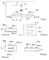
- FIG. 1 shows a part of a suppression device integrated monolithically in an integrated circuit IC according to the invention, which has a strip line 20a, wherein a signal terminal of the circuit formed as a bonding pad 10 is connected via a coupling capacitor C_1 to the beginning of a first section 21a of the strip line 20a. At the end of section 21a, stripline 20a is shorted to ground GND. A signal line connected to the bond pad 10 is indicated in FIG. 1 by the line 11.
- the strip line 20a has the signal conductor 20a_1 already shown in FIG. 1 as well as an associated ground conductor 20a_2 not shown in FIG. 1, which can be seen from the cross section of the strip line 20a shown in FIG. 2a. Between the conductors 20a_1, 20a_2 of the strip line 20a is located as a dielectric oxide layer Ox, which is a part of the monolithic integrated circuit.
- the frequency or wavelength ⁇ for which stripline 20a is to operate as a ⁇ / 2 transformer, is selected as a function of an interference signal which is applied to bonding pad 10, e.g. is applied in the form of a conducted fault or due to interference, and is to be reduced or suppressed by the suppression device according to the invention. Due to the relatively narrowband effect of the formed by the stripline 20a ⁇ / 2 transformer targeted interference suppression for a particular frequency or wavelength is possible.
- FIG. 3 shows a power density spectrum measured in the region of the bond pad 10 (FIG. 1), in which a power density S is plotted over the frequency f.
- the curve labeled S_1 indicates the power density spectrum for the case in which no suppression device according to the invention is provided in the circuit.
- the power density S_1 in this case exceeds a permissible maximum value S_0, in particular in a frequency range around the frequency f_0.
- a further section 21b is provided in addition to the section 21a, which extends from the beginning of the section 21a to the right in FIG. 1 and is also short-circuited to ground GND at its end.
- the second section 21b of the stripline 20a preferably has a length different from the length 1 of the first section 21a, and can thus be used as a ⁇ / 2 transformer for a further frequency of interference radiation to be suppressed.
- the sections 21a, 21b of the stripline 20a form a parallel circuit of a short circuit realized by the first section 21a designed as a ⁇ / 2 transformer for the frequency f_0, and one of Zero different impedance, which is realized by the second portion 21b, because the second portion is formed as a ⁇ / 2 transformer for a different frequency. That is, the two sections 21 a, 21 b of the strip line 20 a do not influence each other their effect as a ⁇ / 2 transformer for the respective frequency.
- the inventive combination of the sections 21a, 21b, the bandwidth of the inventive suppression device can be increased.
- the strip line 20a has only one of the two sections 21a, 21b.
- FIG. 2b shows a layer structure of a part of the circuit according to the invention, in which a total of three metallization levels M_1, M_2, M_3 are arranged one above the other within an oxide layer Ox.
- M_1, M_2, M_3 are arranged one above the other within an oxide layer Ox.
- the strip line 20a shown in FIG. 1 is realized in the metallization planes M_1, M_2 from FIG. 2b and an oxide layer arranged therebetween according to the present exemplary embodiment.
- the ground conductor 20a_2 (FIG. 2a) of the stripline 20a is realized in the first metallization level M_1 according to FIG. 2b
- the signal conductor 20a_1 (FIG. 2a) of the stripline 20a is arranged in the second metallization level M_2 according to FIG. 2b, which is shown in FIG first metallization M_1 is indicated.
- a connection of a conductor 20a_1, 20a_2 of the strip line 20a to a ground potential and / or to the coupling capacitor C_1 (FIG. 1) or to another connection point is realized by means of vias, not shown, in a conventional manner.
- the strip line 20a in the circuit to arrange.
- different metallization levels M_1, M_2, M_3 of the circuit can be used to realize the respective conductors 20a_1, 20a_2 of the strip line 20a, so that there are many possibilities in the interference suppression device according to the invention, the strip line 20a in the circuit to arrange.
- the signal conductor 20b_3 is located between the two grounding conductors 20b_1, 20b_2 and is thus particularly well shielded from other parts of the circuit in a strip line designed as a triplate line 20b, the cross section for illustration in FIG. 2c.
- the signal conductor 20b_3 of the triplate line 20b shown in FIG. 2c can be connected, for example, in the second metallization level M_2 of the circuit, cf. 2b, while the ground conductors 20b_1, 20b_2 are realized in the first and third metallization levels M_1, M_3 of the circuit.
- both the signal conductor 20c_1 and the two ground conductors surrounding the signal conductor are located 20c_2, 20c_3 in the same metallization level of the circuit, which may, for example, be the first metallization level M_1 according to FIG. 2b. Accordingly, the coplanar line 20c for the realization of the suppression device according to the invention particularly useful in circuits usable, which have only a single metallization.
- a plurality of strip lines 20a, 20b, 20c can also be provided in the interference suppression device according to the invention and monolithically integrated into the integrated circuit, wherein, for example, one strip line 20a, 20b, 20c each is connected to a bond pad 10 to be protected against interference radiation or another connection of the circuit can.
- a plurality of preferably different electrical lengths strip lines 20a, 20b, 20c may be connected to a bonding pad 10, so that these different strip lines 20a, 20b, 20c each act for different frequencies as a ⁇ / 2 transformer and a single stripline a enable broadband interference suppression at the bondpad 10.
- a characteristic impedance of the stripline 20a, 20b, 20c is selected so that at the beginning of the portion 21a, 2 1 b ( Figure 1) for a given frequency power adjustment is given, so that a maximum Disturbing power can be dissipated by the bonding pad 10.
- different strip lines 20a, 20b, 20c of the interference suppression device according to the invention are equipped with different lengths.
- different strip lines 20a, 20b, 20c each have different characteristic impedances. Different characteristic impedances can be achieved, for example, by changing the geometry of the conductors of the respective stripline 20a, 20b, 20c or by a corresponding selection of the dielectric disposed between the conductors of the stripline 20a, 20b, 20c.
- a plurality of signal terminals 10 of the circuit can also be connected to the same stripline 20a.
- a strip line 20a of the suppression device can simultaneously serve for suppressing two or more signal terminals 10 of the circuit.
- a plurality of ground conductors 20a_2, 20b_2, 20c_2, 20c_3 of different strip lines 20a, 20b, 20c according to FIG. 4 are each arranged next to one another or orthogonal to one another and connected to a ground potential GND of the circuit and thus form a shielding matrix AT THE.
- the ground conductors 20a_2, 20b_2 and further ground conductors arranged in parallel therewith and unspecified form a group of ground conductors arranged horizontally in FIG. 4, all of which are connected to the ground potential GND of the circuit.
- the ground conductors 20c_2, 20c_3 and other, not shown in more detail in Figure 4 designated ground conductors are provided, which are also all connected to the ground potential GND of the circuit.
- the ground conductors 20a_2, 20b_2 arranged horizontally in FIG. 4 are realized, for example, in a first metallization plane M_1 (FIG. 2b) of the circuit, while the ground conductors 20c_2, 20c_3 shown vertically in FIG.
- the shield matrix AM formed from the ground conductors provides effective protection the circuit according to the invention against interference or spurious emission.
- Frequency-selective interference suppression by forming stripline 20a as a ⁇ / 2 transformer, as described above with reference to FIG. 1, is not impaired by the configuration of the ground conductors shown in FIG.
- the signal conductors belonging to the ground conductors 20a_2, 20b_2, 20c_2, 20c_3 shown in FIG. 4 are not shown in FIG. 4, but depending on the embodiment of the stripline in question may be arranged in further metallization levels of the circuit or in the same plane as the associated ground conductor.
- the shielding matrix AM according to the invention is particularly advantageously arranged in a targeted manner in a region of the circuit which is to be protected against interference radiation or whose interference emission is to be reduced.
- FIG. 5 contains a greatly simplified plan view of the integrated circuit IC according to the invention, which has a plurality of components 100, 110, 120.
- the component 120 is an integrated into the circuit IC oscillator, which is provided for example for generating a reference signal for the circuit IC and the interference radiation of a frequency f_0 ( Figure 3) emits.
- the shielding matrix AM is arranged within the circuit IC such that it at least partially covers the oscillator 120.
- a distance of the ground conductors 20a_2, 20b_2, 20c_2, 20c_3 (FIG. 4) with one another is selected as a function of the frequency f_0 of the interference radiation to be shielded.
- the shielding matrix AM according to the invention introduces an at least partial shielding of the circuit IC according to the Faraday principle, which in comparison to the interference suppression by means of a ⁇ / 2 transformer stripline 20a is relatively broadband.
- the shielding matrix AM In addition to a shield of interference, emanating from the oscillator 120, is through the shielding matrix AM according to the invention also achieves a shielding of interfering radiation acting on the oscillator 120.
- the shielding matrix AM according to the invention can also be arranged over other components 100, 110 of the circuit IC in order to protect it from interference from external components or other interferers or the like.
- the frequency-selective interference suppression according to FIG. 1 is furthermore given by the individual strip lines of the shielding matrix AM.
- all conductors of the strip line 20a are connected to one another and / or to a ground potential GND, in particular directly in the region of a first bond pad 10 (FIG. 1), the first bond pad 10 preferably being connected to the strip line 20a via a coupling capacitor C_1 is connected to the ground potential GND. That is, in contrast to the embodiment depicted in Figure 1, the beginning of portion 21a is shorted to ground GND directly in the region of coupling capacitor C_1, and an output of e.g.
Landscapes
- Physics & Mathematics (AREA)
- Electromagnetism (AREA)
- Condensed Matter Physics & Semiconductors (AREA)
- General Physics & Mathematics (AREA)
- Engineering & Computer Science (AREA)
- Computer Hardware Design (AREA)
- Microelectronics & Electronic Packaging (AREA)
- Power Engineering (AREA)
- Semiconductor Integrated Circuits (AREA)
Abstract
Description
Die Erfindung betrifft eine monolithisch integrierte Schaltung mit mindestens einem ein Signal führenden Signalanschluss und mit einer in die Schaltung integrierten Entstörvorrichtung zur Verringerung von Störstrahlung.The invention relates to a monolithic integrated circuit having at least one signal terminal carrying a signal and with a suppression device integrated in the circuit for reducing interference radiation.
Schaltungen dieser Art sind per se bekannt und basieren im Wesentlichen auf einer Abschirmung von vor Störstrahlung zu schützenden Elementen mittels elektrischer Leiter, die möglichst großflächig um die betreffenden Elemente anzuordnen und mit einem Bezugspotential, insbesondere einem Massepotential der Schaltung, zu verbinden sind.Circuits of this type are known per se and are based essentially on a shielding of elements to be protected against interference by means of electrical conductors which are as large as possible to arrange the respective elements and to be connected to a reference potential, in particular a ground potential of the circuit.
Ein Beispiel für eine derartige herkömmliche Schaltung ist in der
Die beschriebene Anordnung sowie weitere herkömmliche Schaltungen, welche nach dem Faraday-Prinzip abgeschirmt werden, haben den Nachteil, dass einerseits eine verhältnismäßig große Metallfläche innerhalb der integrierten Schaltung zur Ausbildung von abschirmenden Leitern verwendet wird und dass andererseits keine gezielte Verringerung von Störstrahlung und/oder leitungsgebundenen Störungen bestimmter Frequenzen möglich ist.The described arrangement and other conventional circuits, which are shielded according to the Faraday principle, have the disadvantage that on the one hand a relatively large metal surface is used within the integrated circuit for forming shielding conductors and on the other hand, no targeted reduction of interference and / or conducted Disturbances of certain frequencies is possible.
Demgemäß ist es Aufgabe der vorliegenden Erfindung, eine monolithisch integrierte Schaltung der eingangs genannten Art derart zu verbessern, dass eine Verringerung von Störstrahlung bzw. leitungsgebundenen Störungen in einem vorgebbaren Frequenzbereich möglich ist und gleichzeitig eine im Vergleich zu herkömmlichen Schaltungen verhältnismäßig geringe Metallfläche in der integrierten Schaltung verwendet wird.Accordingly, it is an object of the present invention to improve a monolithic integrated circuit of the type mentioned in such a way that a reduction of interference or conducted interference in a predetermined frequency range is possible and at the same time compared to conventional circuits relatively small metal surface in the integrated circuit is used.
Diese Aufgabe wird bei der Schaltung der eingangs genannten Art erfindungsgemäß dadurch gelöst, dass die Entstörvorrichtung mindestens eine Streifenleitung mit einem Abschnitt aufweist, dessen Anfang mit dem Signalanschluss gekoppelt ist, und dessen Ende kurzgeschlossen ist, wobei eine Länge des Abschnitts in Abhängigkeit einer vorgebbaren Frequenz, insbesondere in Abhängigkeit einer zu unterdrückenden Frequenz der Störstrahlung, gewählt ist.This object is achieved in the circuit of the type mentioned in the present invention, that the suppression device comprises at least one stripline having a portion whose beginning is coupled to the signal terminal, and whose end is short-circuited, wherein a length of the section in response to a predetermined frequency, in particular as a function of a frequency of the interference to be suppressed, is selected.
Bevorzugt wird die Länge des Abschnitts der Streifenleitung so gewählt, dass sie einem ganzzahligen Vielfachen derjenigen halben Wellenlänge entspricht, die mit einer zu unterdrückenden Frequenz der Störstrahlung korrespondiert. Auf diese Weise wird der an dem Ende des Abschnitts angeordnete Kurzschluss durch die erfindungsgemäße Streifenleitung wieder in einen Kurzschluss an dem Anfang des Abschnitts der Streifenleitung transformiert, so dass bspw. von dem Signalanschluss in die Streifenleitung eingekoppelte Störsignale der entsprechenden Frequenz durch die erfindungsgemäße Streifenleitung an dem Anfang des Abschnitts kurzgeschlossen werden.Preferably, the length of the section of the stripline is chosen such that it corresponds to an integer multiple of that half wavelength, which corresponds to a frequency of the interference radiation to be suppressed. In this way, the short circuit arranged at the end of the section is transformed again by the stripline according to the invention into a short circuit at the beginning of the section of the stripline, so that, for example, interfering signals of the corresponding frequency coupled from the signal terminal into the stripline are applied to the stripline according to the invention Short-circuited at the beginning of the section.
Durch die verhältnismäßig schmalbandige Wirkung des auf diese Weise durch die erfindungsgemäße Streifenleitung realisierten λ/2-Transformators ist eine gezielte Unterdrückung von Störstrahlung bzw. Störsignalen derjenigen Frequenz möglich, für die der λ/2-Transformator ausgelegt worden ist. Im Gegensatz zu einer externen, d.h. z.B. die Schaltung komplett umgebenden Abschirmung, ermöglicht die Erfindung eine Störunterdrückung direkt innerhalb der monolithisch integrierten Schaltung.Due to the relatively narrow-band effect of the realized in this way by the stripline according to the invention λ / 2 transformer targeted suppression of interference or interference signals that frequency is possible for the λ / 2 transformer has been designed. Unlike an external, i. e.g. The circuit completely surrounding the shield, the invention allows interference suppression directly within the monolithic integrated circuit.
Eine derartige frequenzselektive Störunterdrückung ist insbesondere dann zweckmäßig, wenn die erfindungsgemäße Schaltung zum Einsatz in Systemen vorgesehen ist, bei denen Hochfrequenz-Störquellen bekannter Frequenz wie z.B. Oszillatoren oder dergleichen verwendet werden. Durch eine entsprechende Auslegung der erfindungsgemäßen Streifenleitung kann die Entstörvorrichtung so eingerichtet werden, dass eine maximale Unterdrückung einer bestimmten Frequenz der von der Hochfrequenz-Störquelle ausgehenden Störstrahlung möglich ist.Such frequency-selective interference suppression is particularly useful when the circuit according to the invention is intended for use in systems in which high-frequency interference sources of known frequency, such as e.g. Oscillators or the like can be used. By an appropriate design of the stripline according to the invention, the suppression device can be set up so that a maximum suppression of a certain frequency of emanating from the high-frequency interference source interference is possible.
Bei einem bekannten Leistungsdichtespektrum der Störstrahlung, wie es zur Veranschaulichung in Figur 3 abgebildet ist, kann die Leistungsdichte auf die vorstehend beschriebene Weise über einen bestimmten Frequenzbereich gezielt beeinflusst werden, beispielsweise um bei vorgegebenen Frequenzen einzuhaltende Maximalwerte der Leistungsdichte nicht zu überschreiten.In the case of a known power density spectrum of the interference radiation, as illustrated in FIG. 3 for the purpose of illustration, the power density can be influenced in a targeted manner over a certain frequency range in the manner described above, for example in order not to exceed the maximum power density values to be maintained at predetermined frequencies.
Bei einer vorteilhaften Ausführungsform der vorliegenden Erfindung ist ein Wellenwiderstand der Streifenleitung so gewählt, dass an dem Anfang des Abschnitts für eine vorgebbare Frequenz Leistungsanpassung gegeben ist. Bei dieser Erfindungsvariante ist sichergestellt, dass eine maximale Störleistung in die erfindungsgemäße Streifenleitung eingekoppelt und damit von dem Signalanschluss abgeführt wird.In an advantageous embodiment of the present invention, a characteristic impedance of the stripline is selected such that power adaptation is provided at the beginning of the section for a predefinable frequency. In this variant of the invention, it is ensured that a maximum interference power is coupled into the stripline according to the invention and thus removed from the signal terminal.
Bei einer weiteren, ganz besonders vorteilhaften Ausführungsform der vorliegenden Erfindung ist ein erster Leiter der Streifenleitung in einer ersten Metallisierungsebene der Schaltung angeordnet, und ein zweiter Leiter derselben Streifenleitung ist in einer zweiten Metallisierungsebene der Schaltung angeordnet. Bei dieser Konfiguration der erfindungsgemäßen Streifenleitung bildet eine zwischen den beiden Metallisierungsebenen angeordnete Isolierschicht, bei der es sich beispielsweise um eine Oxidschicht der Schaltung handelt, das u.a. den Wellenwiderstand der Streifenleitung beeinflussende Dielektrikum. Die effektive Dielektrizitätszahl der Streifenleitung kann über die Wahl der zwischen den Metallisierungsebenen befindlichen Isolierschicht oder auch durch die Geometrie der einzelnen Leiter der Streifenleitung beeinflusst werden. Ausgehend von einer vorgegebenen Geometrie der Leiter der Streifenleitung kann ein resultierender Wellenwiderstand der Streifenleitung beispielsweise mit einer der bekannten Näherungsformeln abgeschätzt werden. Aufgrund der Integration der Streifenleitung in die monolithisch integrierte Schaltung können sich jedoch je nach Realisierung der Schaltung z.B. abweichende Wellenwiderstände ergeben, weswegen eine numerische Simulation einer geplanten erfindungsgemäßen Entstörvorrichtung zweckmäßig ist.In a further, particularly advantageous embodiment of the present invention, a first conductor of the stripline is arranged in a first metallization level of the circuit, and a second conductor of the same stripline is arranged in a second metallization level of the circuit. In this configuration of the stripline according to the invention forms one between the two metallization levels arranged insulating layer, which is, for example, an oxide layer of the circuit, inter alia, the characteristic impedance of the strip line affecting dielectric. The effective dielectric constant of the stripline can be influenced by the choice of the insulating layer located between the metallization levels or also by the geometry of the individual conductors of the stripline. Starting from a predetermined geometry of the conductors of the stripline, a resulting characteristic impedance of the stripline can be estimated, for example, with one of the known approximation formulas. Due to the integration of the stripline into the monolithically integrated circuit, however, depending on the implementation of the circuit, for example, deviating characteristic impedances may result, for which reason a numerical simulation of a planned interference suppression device according to the invention is expedient.
Bei einer weiteren, besonders vielseitigen Ausführungsform der erfindungsgemäßen Entstörvorrichtung ist die Streifenleitung als Koplanarleitung ausgebildet, bei der alle Leiter der Streifenleitung in einer einzigen Metallisierungsebene der Schaltung angeordnet sind. Durch die Ausbildung der Streifenleitung als Koplanarleitung kann die erfindungsgemäße Entstörvorrichtung auch bei monolithisch integrierten Schaltungen vorgesehen werden, die nur eine einzige Metallisierungsebene aufweisen.In a further, particularly versatile embodiment of the interference suppression device according to the invention, the strip line is designed as a coplanar line, in which all conductors of the strip line are arranged in a single metallization plane of the circuit. Due to the design of the stripline as a coplanar line, the interference suppression device according to the invention can also be provided in monolithically integrated circuits which have only a single metallization level.
In vorteilhafter Weiterbildung der vorliegenden Erfindung ist es auch möglich, dass die Streifenleitung als eine drei Leiter umfassende Triplate-Leitung ausgebildet ist, bei der ein erster Masseleiter und ein zweiter Masseleiter der Triplate-Leitung jeweils in verschiedenen Metallisierungsebenen angeordnet ist. Ein Signalleiter der Triplate-Leitung ist zwischen den die Masseleiter aufnehmenden Metallisierungsebenen, vorzugsweise in einer weiteren Metallisierungsebene, angeordnet. Bei der Verwendung der vorstehend beschriebenen Triplate-Leitung ergibt sich eine besonders effektive Abschirmung des Signalleiters.In an advantageous embodiment of the present invention, it is also possible that the strip line is formed as a tri-conductor comprising three conductors, in which a first ground conductor and a second ground conductor of the triplate line is arranged in different metallization levels. A signal conductor of the triplate line is arranged between the metallization planes receiving the ground conductors, preferably in a further metallization plane. When using the triplate line described above results in a particularly effective shielding of the signal conductor.
Eine andere vorteilhafte Ausführungsform der vorliegenden Erfindung sieht mehrere Streifenleitungen vor, die bspw. für einen einzigen Signalanschluss der Schaltung als jeweils bei unterschiedlichen Frequenzen bzw. Wellenlängen arbeitende λ/2-Transformatoren eingesetzt werden können. Mit einer derartigen Anordnung ist es möglich, gleichzeitig gezielt mehrere vorgebbare Frequenzen der Störstrahlung zu unterdrücken und somit eine breitbandigere Entstörung zu ermöglichen, verglichen mit dem Einsatz einer einzigen Streifenleitung.Another advantageous embodiment of the present invention provides a plurality of strip lines, which can be used, for example, for a single signal terminal of the circuit as λ / 2 transformers operating at different frequencies or wavelengths. With such an arrangement, it is possible to simultaneously suppress a plurality of predetermined frequencies of the interference radiation and thus a broadband interference suppression, compared to the use of a single stripline.
Um die mehreren Streifenleitungen für verschiedene Frequenzen jeweils als λ/2-Transformator auszubilden sind die Längen der jeweiligen Streifenleitung entsprechend der zu unterdrückenden Frequenz bzw. Wellenlänge zu wählen. Ferner ist es, bspw. durch die Wahl von Isolierschichtbereichen mit unterschiedlicher Dielektrizitätszahl, möglich, verschiedene Streifenleitungen mit einem unterschiedlichen Wellenwiderstand zu versehen. Darüber hinaus kann der Wellenwiderstand jeder Streifenleitung individuell durch die entsprechende Wahl der Geometrie der jeweiligen Leiter eingestellt werden.In order to form each of the several strip lines for different frequencies as a λ / 2 transformer, the lengths of the respective strip line are to be selected according to the frequency or wavelength to be suppressed. Furthermore, it is possible, for example by the choice of insulating layer regions with different dielectric constant, to provide different strip lines with a different characteristic impedance. In addition, the characteristic impedance of each stripline can be adjusted individually by the appropriate choice of the geometry of the respective conductor.
Erfindungsgemäß ist es auch möglich, eine einzige Streifenleitung derart vorzusehen, dass zwei verschiedene Abschnitte der Streifenleitung hinsichtlich ihrer Länge bis zu dem jeweiligen Ende oder hinsichtlich ihres Wellenwiderstands jeweils unterschiedlich konfiguriert sind, so dass auf diese Weise mit einer einzigen Streifenleitung insgesamt z.B. zwei λ/2-Transformatoren realisierbar sind, die jeweils für verschiedene Frequenzen ausgelegt sind. Bei dieser Konfiguration ist der Anfang beider Abschnitte jeweils in bekannter Weise mit dem Signalanschluss der Schaltung gekoppelt, während z.B. die Länge des ersten Abschnitts von der Länge des zweiten Abschnitts, der ebenfalls an seinem Ende kurzgeschlossen ist, verschieden ist. In diesem Fall stellt also jeder der beiden Abschnitte der Streifenleitung einen separaten λ/2-Transformator für die entsprechende Wellenlänge bzw. Frequenz dar.According to the invention, it is also possible to provide a single stripline such that two different sections of the stripline are each differently configured in their length to the respective end or in terms of their characteristic impedance, so that in this way with a single stripline in total e.g. two λ / 2 transformers can be realized, which are each designed for different frequencies. In this configuration, the beginning of both sections are each coupled in a known manner to the signal terminal of the circuit, while e.g. the length of the first section is different from the length of the second section, which is also shorted at its end. In this case, therefore, each of the two sections of the stripline represents a separate λ / 2 transformer for the corresponding wavelength or frequency.
Bei einer weiteren vorteilhaften Ausführungsform der vorliegenden Erfindung ist die Streifenleitung über Mittel zur kapazitiven Kopplung mit dem Signalanschluss verbunden. Durch die Hochpasscharakteristik einer kapazitiven Kopplung wird verhindert, dass ein niederfrequentes Nutzsignal von dem Signalanschluss der Schaltung in die Streifenleitung der Entstörvorrichtung einkoppelt, während jedoch hochfrequente Störsignale von dem Signalanschluss zu der Streifenleitung abgeführt werden können. Eine zur Realisierung der kapazitiven Kopplung verwendete Kapazität ist dementsprechend in Abhängigkeit der maximal an dem Signalanschluss auftretenden Frequenzen des Nutzsignals zu wählen.In a further advantageous embodiment of the present invention, the stripline is connected to the signal terminal via means for capacitive coupling. The high-pass characteristic of a capacitive coupling prevents a low-frequency useful signal from the signal terminal of the circuit from being coupled into the strip line of the interference suppression device, while high-frequency interference signals can be removed from the signal terminal to the strip line. A capacitance used for the realization of the capacitive coupling is accordingly to be selected as a function of the maximum frequencies of the useful signal occurring at the signal terminal.
Vorteilhaft können erfindungsgemäß auch mehrere Signalanschlüsse der Schaltung mit derselben Streifenleitung verbunden werden. Auf diese Weise kann eine Streifenleitung der Entstörvorrichtung gleichzeitig zur Entstörung von zwei oder mehr Signalanschlüssen der Schaltung dienen. Entsprechend den vorstehenden Ausführungen sind die jeweiligen Anschlusspunkte vorzugsweise so zu wählen, dass zumindest ein Abschnitt der Streifenleitung für jeweils einen Signalanschluss einen λ/2-Transformator darstellt.Advantageously, according to the invention, a plurality of signal terminals of the circuit can also be connected to the same stripline. In this way, a stripline of the suppression device at the same time serve to suppress interference of two or more signal terminals of the circuit. According to the above explanations, the respective connection points are preferably to be selected so that at least one section of the strip line represents a λ / 2 transformer for each signal connection.
Bei einer weiteren, ganz besonders vorteilhaften Ausführungsform der vorliegenden Erfindung sind die Masseleiter verschiedener Streifenleitungen nebeneinander, insbesondere parallel zueinander, und/oder orthogonal zueinander angeordnet und mit einem Massepotential der Schaltung verbunden, um eine Abschirmungsmatrix zu bilden. Bei dieser Ausführungsform der vorliegenden Erfindung wird die Tatsache ausgenutzt, dass bei dem Vorhandensein mehrerer Streifenleitungen ohnehin eine entsprechende Anzahl von Masseleitern vorhanden ist, die mit einem Massepotential der Schaltung verbunden sind. Diese Masseleiter können neben ihrer Funktion in der jeweiligen Streifenleitung gleichzeitig zusätzlich eine Abschirmfunktion gegen Störstrahlung übernehmen, die besonders wirksam ist, wenn mehrere der Masseleiter nebeneinander, parallel zueinander oder auch orthogonal zueinander angeordnet sind.In a further, particularly advantageous embodiment of the present invention, the ground conductors of different strip lines are arranged side by side, in particular parallel to each other, and / or orthogonal to each other and connected to a ground potential of the circuit to form a shielding matrix. In this embodiment of the present invention, the fact is exploited that in the presence of a plurality of strip lines in any case a corresponding number of ground conductors is present, which are connected to a ground potential of the circuit. In addition to their function in the respective strip line, these grounding conductors can simultaneously additionally assume a shielding function against interfering radiation, which is particularly effective if several of the ground conductors are arranged next to one another, parallel to one another or else orthogonal to one another.
Durch eine derartige Abschirmungsmatrix aus den Masseleitern verschiedener Streifenleitungen ist neben der frequenzselektiven Störunterdrückung an den Signalanschlüssen gleichzeitig eine allgemeine elektrische Abschirmung realisiert, die nach dem Prinzip des Faradayschen Käfigs arbeitet.By such a shielding matrix of the ground conductors of different strip lines in addition to the frequency-selective interference suppression at the signal terminals simultaneously a general electrical shield is realized, which operates on the principle of Faraday cage.
Ganz besonders vorteilhaft deckt die Abschirmungsmatrix eine Komponente der Schaltung zumindest teilweise ab, um auf die Komponente einwirkende Störstrahlung und/oder von der Komponente ausgehende Störschaltung abzuschirmen. Auf diese Weise kann mittels der erfindungsgemäßen Abschirmungsmatrix auch eine Aussendung von Störstrahlung reduziert werden, die von in der Schaltung angeordneten Komponenten ausgeht. Bspw. können insbesondere Komponenten wie integrierte Oszillatoren oder Gleichspannungswandler mittels der Abschirmungsmatrix abgedeckt werden, um eine von der erfindungsgemäßen Schaltung ausgehende Störstrahlung zu vermindern.In a particularly advantageous manner, the shielding matrix at least partially covers a component of the circuit in order to shield interference radiation acting on the component and / or interference circuit emanating from the component. In this way, by means of the shielding matrix according to the invention, it is also possible to reduce emission of interference radiation emanating from components arranged in the circuit. For example. In particular, components such as integrated oscillators or DC-DC converters can be covered by means of the shielding matrix in order to reduce interference emanating from the circuit according to the invention.
Analog zu der Reduzierung von nach außen dringender Störstrahlung ist durch die erfindungsgemäße Abschirmungsmatrix auch ein Schutz der Schaltung bzw. von Komponenten der Schaltung vor Störstrahlung gegeben, die von außen auf die Schaltung eintrifft.Analogous to the reduction of outwardly directed interference radiation, the shielding matrix according to the invention also protects the circuit or components of the circuit from interfering radiation which arrives at the circuit from the outside.
Generell ist die durch die Abschirmungsmatrix realisierte Abschirmwirkung breitbandiger als die Wirkung einer als λ/2-Transformator ausgebildeten Streifenleitung, weil alle diejenigen Frequenzen der Störstrahlung durch die erfindungsgemäße Abschirmungsmatrix abgeschirmt bzw. gedämpft werden, die unterhalb einer bestimmten Grenzfrequenz liegen, die von dem Abstand der Masseleiter der Streifenleitungen untereinander abhängt. Der jeweilige Abstand der Masseleiter untereinander ist dementsprechend vorzugsweise in Abhängigkeit mindestens einer Frequenz von zu unterdrückender bzw. abzuschirmender Störstrahlung zu wählen.In general, the shielding effect realized by the shielding matrix is broader than the effect of a stripline designed as a λ / 2 transformer, because all those frequencies of the interfering radiation are shielded or attenuated by the shielding matrix according to the invention, which are below a certain cutoff frequency, which depends on the distance Ground conductor of the strip lines depends on each other. The respective distance between the ground conductors with one another is accordingly preferably to be selected as a function of at least one frequency of interference radiation to be suppressed or to be shielded.
Zur Bildung der erfindungsgemäßen Abschirmungsmatrix können mehrere Masseleiter in derselben Metallisierungsebene der Schaltung angeordnet sein. Alternativ hierzu ist es auch möglich, mehrere, insbesondere auch parallel zueinander verlaufende Masseleiter, in verschiedenen Metallisierungsebenen der Schaltung vorzusehen, wobei diese untereinander mittels die verschiedenen Metallisierungsebenen verbindenden Kontaktierungen zu verbinden sind.To form the shielding matrix according to the invention, a plurality of ground conductors can be arranged in the same metallization level of the circuit. Alternatively, it is also possible to provide several, in particular also parallel to each other grounding conductor, in different metallization levels of the circuit, which are to be connected to each other by means of the different metallization levels connecting contacts.
Ferner ist es möglich, eine erste Anzahl von Masseleitern in einer ersten Metallisierungsebene der Schaltung anzuordnen, und eine zweite Anzahl von Masseleitern, die beispielsweise jeweils orthogonal zu den Masseleitern der ersten Metallisierungsebene angeordnet sind, in einer zweiten Metallisierungsebene der Schaltung vorzusehen. Die zugehörigen Signalleiter der Streifenleitungen können jeweils in derselben oder auch einer anderen Metallisierungsebene der Schaltung angeordnet sein.Furthermore, it is possible to arrange a first number of ground conductors in a first metallization level of the circuit, and to provide a second number of ground conductors, which are arranged, for example, orthogonal to the ground conductors of the first metallization level, in a second metallization level of the circuit. The associated signal conductors of the strip lines can each be arranged in the same or a different metallization level of the circuit.
Aufgrund der guten Abschirmung des Signalleiters ist eine als Triplate-Leitung ausgeführte Streifenleitung besonders geeignet zum Aufbau der erfindungsgemäßen Abschirmungsmatrix.Due to the good shielding of the signal conductor, a strip line embodied as a triplate line is particularly suitable for constructing the shielding matrix according to the invention.
Bei einer weiteren vorteilhaften Ausführungsform der vorliegenden Erfindung sind alle Leiter der Streifenleitung miteinander und/oder mit einem Massepotential verbunden. Insbesondere können bei dieser Ausführungsform die Leiter auch direkt im Bereich des Signalanschlusses miteinander verbunden sein, so dass der betreffende Signalanschluss über die Mittel zur kapazitiven Kopplung direkt mit einem Massepotential verbunden ist, wodurch alle eine durch die Kopplungskapazität definierte Grenzfrequenz übersteigenden Frequenzen von dem Signalanschluss direkt nach Masse abgeleitet werden.In a further advantageous embodiment of the present invention, all Head of stripline connected to each other and / or to a ground potential. In particular, in this embodiment, the conductors can also be connected to each other directly in the region of the signal terminal, so that the relevant signal terminal is connected directly to a ground potential via the means for capacitive coupling, whereby all exceeding a defined by the coupling capacitance cutoff frequencies from the signal terminal directly after Mass are derived.
Bei einer weiteren Ausführungsform der vorliegenden Erfindung ist der Signalanschluss ein Bondpad der Schaltung. Besonders zweckmäßig wird z.B. bei einer Ausbildung der Schaltung als Transceiver für einen Datenbus ein Bondpad mit der erfindungsgemäßen Entstörvorrichtung verbunden, das ein Kommunikationssignal für die Kommunikation auf dem Datenbus führt und das daher insbesondere leitungsgebundenen Störungen stärker ausgesetzt ist als andere Bondpads der Schaltung. Beispielsweise kann es sich bei der erfindungsgemäßen Schaltung um einen CAN (controller area network)-, LIN (local interconnect network)- oder einen Flexray-Transceiver handeln.In a further embodiment of the present invention, the signal terminal is a bonding pad of the circuit. Particularly useful is e.g. in an embodiment of the circuit as a transceiver for a data bus, a bond pad is connected to the interference suppression device according to the invention, which carries a communication signal for the communication on the data bus and which is therefore more exposed to line-bound interference than other bond pads of the circuit. For example, the circuit according to the invention can be a controller area network (CAN), a local interconnect network (LIN) or a flexray transceiver.
Insgesamt ist mittels der erfindungsgemäßen Entstörvorrichtung eine Reduktion von leitungsgebundenen Störungen, bspw. im Bereich eines Bondpads der Schaltung, möglich sowie eine verhältnismäßig breitbandige Abschirmung zumindest einzelner Komponenten der Schaltung vor Störstrahlung. Durch die Entstörvorrichtung wird sowohl eine Störeinstrahlung in die Schaltung als auch eine von der Schaltung ausgehende Störausstrahlung verringert.Overall, by means of the interference suppression device according to the invention, a reduction of conducted disturbances, for example in the region of a bond pad of the circuit, is possible, as well as a relatively broadband shielding of at least individual components of the circuit against interference radiation. By the suppression device both interference is reduced in the circuit as well as emanating from the circuit spurious emission.
Weitere Vorteile, Merkmale und Einzelheiten ergeben sich aus der nachfolgenden Beschreibung, in der unter Bezugnahme auf die Zeichnung verschiedene Ausführungsbeispiele der Erfindung dargestellt sind. Dabei können die in den Ansprüchen und in der Beschreibung erwähnten Merkmale jeweils einzeln für sich oder in beliebiger Kombination erfindungswesentlich sein.Further advantages, features and details will become apparent from the following description in which, with reference to the drawings, various embodiments of the invention are shown. The features mentioned in the claims and in the description may each be essential to the invention individually or in any desired combination.
In der Zeichnung zeigen:
Figur 1- eine erste Ausführungsform der erfindungsgemäßen Entstörvorrichtung,
- Figur 2a
- einen Querschnitt durch eine erste Ausführungsform einer monolithisch in die erfindungsgemäße Schaltung integrierten Streifenleitung,
- Figur 2b
- einen Schichtaufbau eines Teils der erfindungsgemäßen Schaltung,
- Figur 2c
- einen Querschnitt durch eine zweite Ausführungsform einer monolithisch in die erfindungsgemäße Schaltung integrierten Streifenleitung,
- Figur 2d
- einen Querschnitt durch eine weitere Ausführungsform einer monolithisch in die erfindungsgemäße Schaltung integrierten Streifenleitung,
Figur 3- ein Leistungsdichtespektrum von Störstrahlung,
- Figur 4
- eine durch mehrere Masseleiter von in der Schaltung vorgesehenen Streifenleitungen gebildete Abschirmungsmatrix, und
- Figur 5
- eine Ausführungsform der erfindungsgemäßen Schaltung mit einer Abschirmungsmatrix gemäß Figur 4.
- FIG. 1
- a first embodiment of the suppression device according to the invention,
- FIG. 2a
- a cross section through a first embodiment of a monolithic integrated in the circuit according to the invention stripline,
- FIG. 2b
- a layer structure of a part of the circuit according to the invention,
- Figure 2c
- a cross section through a second embodiment of a monolithic integrated in the circuit according to the invention stripline,
- Figure 2d
- a cross-section through a further embodiment of a monolithic integrated in the circuit according to the invention stripline
- FIG. 3
- a power density spectrum of interference radiation,
- FIG. 4
- a shielding matrix formed by a plurality of ground conductors of strip lines provided in the circuit, and
- FIG. 5
- an embodiment of the circuit according to the invention with a shielding matrix according to Figure 4.
Figur 1 zeigt einen Teil einer monolithisch in eine erfindungsgemäße integrierte Schaltung IC integrierten Entstörvorrichtung, die eine Streifenleitung 20a aufweist, wobei ein als Bondpad 10 ausgebildeter Signalanschluss der Schaltung über einen Koppelkondensator C_1 mit dem Anfang eines ersten Abschnitts 21 a der Streifenleitung 20a verbunden ist. An dem Ende des Abschnitts 21a ist die Streifenleitung 20a nach Masse GND kurzgeschlossen. Eine mit dem Bondpad 10 verbundene Signalleitung ist in Figur 1 durch die Linie 11 angedeutet.FIG. 1 shows a part of a suppression device integrated monolithically in an integrated circuit IC according to the invention, which has a
Insgesamt weist die Streifenleitung 20a den bereits in Figur 1 dargestellten Signalleiter 20a_1 sowie einen nicht in Figur 1 abgebildeten zugehörigen Masseleiter 20a_2 auf, der aus dem in Figur 2a gezeigten Querschnitt der Streifenleitung 20a ersichtlich ist. Zwischen den Leitern 20a_1, 20a_2 der Streifenleitung 20a befindet sich als Dielektrikum eine Oxidschicht Ox, die ein Bestandteil der monolithisch integrierten Schaltung ist.Overall, the
Die Länge 1 des Abschnitts 21a der Streifenleitung 20a (Figur 1) ist erfindungsgemäß so gewählt, dass der Kurzschluss nach Masse GND von dem Ende des Abschnitts 21 a durch den Abschnitt 21a der Streifenleitung 20a in einen Kurzschluss an dem Anfang des Abschnitts 21a transformiert wird, der über den Koppelkondensator C_1 mit dem Bondpad 10 der Schaltung verbunden ist. D.h., die erfindungsgemäße Streifenleitung 20a wird als λ/2-Transformator eingesetzt, 1= λ/2.The
Die Frequenz bzw. Wellenlänge λ, für die die Streifenleitung 20a als λ/2-Transformator arbeiten soll, wird in Abhängigkeit eines Störsignals gewählt, das an dem Bondpad 10 z.B. in Form einer leitungsgebundenen Störung oder auch aufgrund einer Störeinstrahlung anliegt, und das durch die erfindungsgemäße Entstörvorrichtung vermindert bzw. unterdrückt werden soll. Aufgrund der verhältnismäßig schmalbandigen Wirkung des durch die Streifenleitung 20a gebildeten λ/2-Transformators ist eine gezielte Störunterdrückung für eine bestimmte Frequenz bzw. Wellenlänge möglich.The frequency or wavelength λ, for which
Die Wirkung der erfindungsgemäßen Entstörvorrichtung ist nachfolgend unter Bezug auf Figur 3 beispielhaft beschrieben. Figur 3 zeigt ein im Bereich des Bondpads 10 (Figur 1) gemessenes Leistungsdichtespektrum, bei dem eine Leistungsdichte S über der Frequenz f aufgetragen ist. Die mit S_1 bezeichnete Kurve gibt hierbei das Leistungsdichtespektrum für denjenigen Fall an, in dem keine erfindungsgemäße Entstörvorrichtung in der Schaltung vorgesehen ist. Wie aus Figur 3 ersichtlich, überschreitet die Leistungsdichte S_1 in diesem Fall insbesondere in einem Frequenzbereich um die Frequenz f_0 einen zulässigen maximalen Wert S_0. Im Gegensatz hierzu ergibt sich bei der Verwendung der erfmdungsgemäßen Entstörvorrichtung und einer entsprechenden Auslegung der Streifenleitung 20a als λ/2-Transformator für die Frequenz f_0 der in Figur 3 durch die gestrichelte Kurve S_2 angedeutete Verlauf des Leistungsdichtespektrums. Der Einsatz der erfindungsgemäßen Entstörvorrichtung, die in Form der beschriebenen Streifenleitung 20a monolithisch in die integrierte Schaltung integriert wird, ermöglicht demzufolge eine effiziente Unterdrückung beziehungsweise Verminderung von Störstrahlung im Bereich des Bondpads 10.The effect of the suppression device according to the invention is described below by way of example with reference to FIG. FIG. 3 shows a power density spectrum measured in the region of the bond pad 10 (FIG. 1), in which a power density S is plotted over the frequency f. The curve labeled S_1 indicates the power density spectrum for the case in which no suppression device according to the invention is provided in the circuit. As can be seen from FIG. 3, the power density S_1 in this case exceeds a permissible maximum value S_0, in particular in a frequency range around the frequency f_0. In contrast, results in the use of the inventive interference suppression and a corresponding design of the
Neben leitungsgebundenen Störungen, die über den Koppelkondensator C_1 (Figur 1) direkt zu der Streifenleitung 20a abgeführt werden, können durch die erfindungsgemäße Entstörvorrichtung auch auf das Bondpad 10 beziehungsweise dessen ggf. vorhandene elektrische Zuleitungen 11 wie beispielsweise Bonddrähte und dergleichen einwirkende Störstrahlungskomponenten vermindert beziehungsweise unterdrückt werden. Mit der erfindungsgemäßen Entstörvorrichtung sind sowohl von außen in die Schaltung eingestrahlte Störstrahlungskomponenten sowie beispielsweise von in der Schaltung vorgesehenen aktiven Komponenten ausgehende Störstrahlung unterdrückbar.In addition to conducted interference, which are discharged via the coupling capacitor C_1 (Figure 1) directly to the
Bei der in Figur 1 abgebildeten Streifenleitung 20a ist neben dem Abschnitt 21a ein weiterer Abschnitt 21b vorgesehen, der sich von dem Anfang des Abschnitts 21a ausgehend in Figur 1 nach rechts erstreckt und an seinem Ende ebenfalls nach Masse GND kurzgeschlossen ist. Der zweite Abschnitt 21 b der Streifenleitung 20a weist vorzugsweise eine von der Länge 1 des ersten Abschnitts 21 a verschiedene Länge auf, und kann somit als λ/2-Transformator für eine weitere Frequenz von zu unterdrückender Störstrahlung eingesetzt werden.In the case of the
Für zu unterdrückende Störsignale einer ersten Frequenz f_0 (Figur 3) bilden die Abschnitte 21a, 21b der Streifenleitung 20a eine Parallelschaltung aus einem Kurzschluss, der durch den als λ/2-Transformator für die Frequenz f_0 ausgebildeten ersten Abschnitt 21a realisiert wird, und einer von Null verschiedenen Impedanz, die durch den zweiten Abschnitt 21b realisiert wird, weil der zweite Abschnitt als λ/2-Transformator für eine andere Frequenz ausgebildet ist. Das heißt, die beiden Abschnitte 21 a, 21b der Streifenleitung 20a beeinflussen sich gegenseitig ihrer Wirkung als λ/2-Transformator für die jeweilige Frequenz nicht.For suppressing spurious signals of a first frequency f_0 (FIG. 3), the sections 21a, 21b of the
Durch die erfindungsgemäße Kombination der Abschnitte 21a, 21b kann die Bandbreite der erfmdungsgemäßen Entstörvorrichtung gesteigert werden.The inventive combination of the sections 21a, 21b, the bandwidth of the inventive suppression device can be increased.
Alternativ hierzu ist es jedoch auch möglich, dass die Streifenleitung 20a lediglich einen der beiden Abschnitte 21 a, 21b aufweist.Alternatively, however, it is also possible that the
Figur 2b zeigt einen Schichtaufbau eines Teils der erfindungsgemäßen Schaltung, bei dem innerhalb einer Oxidschicht Ox insgesamt drei Metallisierungsebenen M_1, M_2, M_3 jeweils übereinander angeordnet sind. Ein bei der Darstellung nach Figur 2b unterhalb der Oxidschicht Ox angeordnetes Substrat, das aktive Komponenten der erfindungsgemäßen Schaltung wie beispielsweise Transistoren, Spannungsregler, Oszillatoren oder dergleichen enthält, ist in Figur 2b nicht abgebildet.FIG. 2b shows a layer structure of a part of the circuit according to the invention, in which a total of three metallization levels M_1, M_2, M_3 are arranged one above the other within an oxide layer Ox. A in the illustration of Figure 2b below the oxide layer Ox arranged substrate, the active components of the invention Circuit such as transistors, voltage regulators, oscillators or the like, is not shown in Figure 2b.
Die in Figur 1 abgebildete Streifenleitung 20a ist gemäß dem vorliegenden Ausführungsbeispiel in den Metallisierungsebenen M_1, M_2 aus Figur 2b und einer dazwischen angeordneten Oxidschicht realisiert. Beispielsweise ist der Masseleiter 20a_2 (Figur 2a) der Streifenleitung 20a in der ersten Metallisierungsebene M_1 gemäß Figur 2b realisiert, während der Signalleiter 20a_1 (Figur 2a) der Streifenleitung 20a in der zweiten Metallisierungsebene M_2 gemäß Figur 2b angeordnet ist, die in Figur 2b oberhalb der ersten Metallisierungsebene M_1 angedeutet ist.The
Eine Verbindung eines Leiters 20a_1, 20a_2 der Streifenleitung 20a zu einem Massepotential und/oder zu dem Koppelkondensator C_1 (Figur 1) oder zu einem sonstigen Anschlusspunkt ist durch nicht abgebildete Durchkontaktierungselemente, Vias, in herkömmlicher Weise realisiert.A connection of a conductor 20a_1, 20a_2 of the
Generell können je nach Ausbildung der Streifenleitung 20a verschiedene Metallisierungsebenen M_1, M_2, M_3 der Schaltung verwendet werden, um die jeweiligen Leiter 20a_1, 20a_2 der Streifenleitung 20a zu realisieren, so dass sich bei der erfindungsgemäßen Entstörvorrichtung vielfältige Möglichkeiten ergeben, die Streifenleitung 20a in der Schaltung anzuordnen.Generally, depending on the design of the
Bei einer als Triplate-Leitung ausgebildeten Streifenleitung 20b, deren Querschnitt zur Veranschaulichung in Figur 2c abgebildet ist, befindet sich der Signalleiter 20b_3 zwischen den beiden Masseleitern 20b_1, 20b_2 und ist auf diese Weise besonders gut von weiteren Teilen der Schaltung abgeschirmt. Der Signalleiter 20b_3 der in Figur 2c gezeigten Triplate-Leitung 20b kann beispielsweise in der zweiten Metallisierungsebene M_2 der Schaltung, vgl. Figur 2b, angeordnet sein, während die Masseleiter 20b_1, 20b_2 in der ersten und dritten Metallisierungsebene M_1, M_3 der Schaltung realisiert sind.2c, the signal conductor 20b_3 is located between the two grounding conductors 20b_1, 20b_2 and is thus particularly well shielded from other parts of the circuit in a strip line designed as a triplate line 20b, the cross section for illustration in FIG. 2c. The signal conductor 20b_3 of the triplate line 20b shown in FIG. 2c can be connected, for example, in the second metallization level M_2 of the circuit, cf. 2b, while the ground conductors 20b_1, 20b_2 are realized in the first and third metallization levels M_1, M_3 of the circuit.
Bei einer als Koplanarleitung ausgebildeten Streifenleitung 20c nach Figur 2d befindet sich sowohl der Signalleiter 20c_1 als auch die beiden den Signalleiter umgebenden Masseleiter 20c_2, 20c_3 in derselben Metallisierungsebene der Schaltung, bei der es sich beispielsweise um die erste Metallisierungsebene M_1 gemäß Figur 2b handeln kann. Demgemäß ist die Koplanarleitung 20c zur Realisierung der erfindungsgemäßen Entstörvorrichtung besonders zweckmäßig in Schaltungen verwendbar, die nur eine einzige Metallisierungsebene aufweisen.In a
Generell können bei der erfindungsgemäßen Entstörvorrichtung auch mehrere Streifenleitungen 20a, 20b, 20c vorgesehen und monolithisch in die integrierte Schaltung integriert sein, wobei beispielsweise jeweils eine Streifenleitung 20a, 20b, 20c mit einem vor Störstrahlung zu schützenden Bondpad 10 oder einem sonstigen Anschluss der Schaltung verbunden sein kann. Ferner können auch mehrere, vorzugsweise verschiedene elektrische Längen aufweisende Streifenleitungen 20a, 20b, 20c mit einem Bondpad 10 verbunden sein, so dass diese verschiedenen Streifenleitungen 20a, 20b, 20c jeweils für verschiedene Frequenzen als λ/2-Transformator wirken und gegenüber einer einzigen Streifenleitung eine breitbandigere Störunterdrückung an dem Bondpad 10 ermöglichen.In general, a plurality of
Bei einer weiteren ganz besonders vorteilhaften Ausführungsform der vorliegenden Erfindung ist ein Wellenwiderstand der Streifenleitung 20a, 20b, 20c so gewählt, dass an dem Anfang des Abschnitts 21a, 2 1 b (Figur 1) für eine vorgebbare Frequenz Leistungsanpassung gegeben ist, so dass eine maximale Störleistung von dem Bondpad 10 abgeführt werden kann.In a further particularly advantageous embodiment of the present invention, a characteristic impedance of the
Neben der Möglichkeit, verschiedene Streifenleitungen 20a, 20b, 20c der erfindungsgemäßen Entstörvorrichtung mit unterschiedlichen Längen auszustatten, ist es erfindungsgemäß auch möglich, dass verschiedene Streifenleitungen 20a, 20b, 20c jeweils unterschiedliche Wellenwiderstände aufweisen. Unterschiedliche Wellenwiderstände können beispielsweise über eine Veränderung der Geometrie der Leiter der betreffenden Streifenleitung 20a, 20b, 20c beziehungsweise durch eine entsprechende Auswahl des zwischen den Leitern der Streifenleitung 20a, 20b, 20c angeordneten Dielektrikums erzielt werden.In addition to the possibility of equipping
Anstelle der in Figur 1 abgebildeten kapazitiven Kopplung des Bondpads 10 zu der Streifenleitung 20a mittels des Koppelkondensators C_1 ist es erfindungsgemäß ferner denkbar, das Bondpad 10 direkt an die Streifenleitung 20a anzuschließen, d.h. galvanisch miteinander zu verbinden. Diese Lösung ist insbesondere dann zweckmäßig, wenn ein an dem Bondpad 10 anliegendes Nutzsignal ein hochfrequentes Bandpaßsignal darstellt, für dessen Signalfrequenzen der an dem Ende des Abschnitts 21a (Figur 1) vorhandene Kurzschluss nach Masse GND durch die Streifenleitung 20a bzw. deren Abschnitt 21 a in eine von Null verschiedene Impedanz transformiert wird, wobei der Koppelkondensator C_1 eingespart werden kann.Instead of the capacitive coupling of the
Vorteilhaft können erfindungsgemäß auch mehrere Signalanschlüsse 10 der Schaltung mit derselben Streifenleitung 20a verbunden werden. Auf diese Weise kann eine Streifenleitung 20a der Entstörvorrichtung gleichzeitig zur Entstörung von zwei oder mehr Signalanschlüssen 10 der Schaltung dienen.Advantageously, according to the invention, a plurality of
Bei einer weiteren sehr vorteilhaften Ausführungsform der vorliegenden Erfindung sind mehrere Masseleiter 20a_2, 20b_2, 20c_2, 20c_3 verschiedener Streifenleitungen 20a, 20b, 20c gemäß Figur 4 jeweils nebeneinander beziehungsweise orthogonal zueinander angeordnet und mit einem Massepotential GND der Schaltung verbunden und bilden auf diese Weise eine Abschirmungsmatrix AM.In a further very advantageous embodiment of the present invention, a plurality of ground conductors 20a_2, 20b_2, 20c_2, 20c_3 of
Wie aus Figur 4 ersichtlich, bilden die Masseleiter 20a_2, 20b_2 sowie dazu parallel angeordnete, nicht näher bezeichnete weitere Masseleiter eine Gruppe von in Figur 4 waagerecht angeordneten Masseleitern, die alle mit dem Massepotential GND der Schaltung verbunden sind. Orthogonal hierzu sind die Masseleiter 20c_2, 20c_3 sowie weitere, nicht näher in Figur 4 bezeichnete Masseleiter vorgesehen, die ebenfalls alle mit dem Massepotential GND der Schaltung verbunden sind. Die in Figur 4 waagerecht angeordneten Masseleiter 20a_2, 20b_2 sind beispielsweise in einer ersten Metallisierungsebene M_1 (Figur 2b) der Schaltung realisiert, während die in Figur 4 vertikal dargestellten Masseleiter 20c_2, 20c_3 in der zweiten Metallisierungsebene M_2 (Figur 2b) der Schaltung realisiert sind. Es ist ferner möglich, die Masseleiter 20a_2, 20b_2, 20c_2, 20c_3 untereinander durch entsprechende Durchkontaktierungen zu verbinden.As can be seen from FIG. 4, the ground conductors 20a_2, 20b_2 and further ground conductors arranged in parallel therewith and unspecified form a group of ground conductors arranged horizontally in FIG. 4, all of which are connected to the ground potential GND of the circuit. Orthogonal thereto, the ground conductors 20c_2, 20c_3 and other, not shown in more detail in Figure 4 designated ground conductors are provided, which are also all connected to the ground potential GND of the circuit. The ground conductors 20a_2, 20b_2 arranged horizontally in FIG. 4 are realized, for example, in a first metallization plane M_1 (FIG. 2b) of the circuit, while the ground conductors 20c_2, 20c_3 shown vertically in FIG. 4 are realized in the second metallization plane M_2 (FIG. 2b) of the circuit. It is also possible to connect the ground conductors 20a_2, 20b_2, 20c_2, 20c_3 with each other by means of corresponding plated-through holes.
Die aus den Masseleitern gebildete Abschirmungsmatrix AM bietet einen wirksamen Schutz der erfindungsgemäßen Schaltung vor Störeinstrahlung beziehungsweise Störausstrahlung. Eine frequenzselektive Störunterdrückung durch eine Ausbildung der Streifenleitung 20a als λ/2-Transformator, wie sie vorstehend unter Bezugnahme auf Figur 1 beschrieben ist, wird durch die in Figur 4 gezeigte Konfiguration der Masseleiter nicht beeinträchtigt. Die zu den in Figur 4 abgebildeten Masseleitern 20a_2, 20b_2, 20c_2, 20c_3 gehörenden Signalleiter sind nicht in Figur 4 abgebildet, können aber je nach Ausführungsform der betreffenden Streifenleitung in weiteren Metallisierungsebenen der Schaltung oder auch in derselben Ebene wie der zugehörige Masseleiter angeordnet sein.The shield matrix AM formed from the ground conductors provides effective protection the circuit according to the invention against interference or spurious emission. Frequency-selective interference suppression by forming
Besonders vorteilhaft wird die erfindungsgemäße Abschirmungsmatrix AM gezielt in einem Bereich der Schaltung angeordnet, der vor Störeinstrahlung geschützt werden soll beziehungsweise dessen Störausstrahlung vermindert werden soll. Eine entsprechende Anordnung ist in Figur 5 wiedergegeben, die eine stark vereinfachte Draufsicht auf die erfindungsgemäße integrierte Schaltung IC enthält, die mehrere Komponenten 100, 110, 120 aufweist. Bei der Komponente 120 handelt es sich um einen in die Schaltung IC integrierten Oszillator, der beispielsweise zur Erzeugung eines Referenzsignals für die Schaltung IC vorgesehen ist und der Störstrahlung einer Frequenz f_0 (Figur 3) abstrahlt. Um die von dem Oszillator 120 ausgehende Störstrahlung so abzuschirmen, dass vorgegebene Grenzwerte für die von der Schaltung IC ausgehende Störabstrahlung nicht überschritten werden, ist die erfindungsgemäße Abschirmungsmatrix AM so innerhalb der Schaltung IC angeordnet, dass sie zumindest teilweise den Oszillator 120 abdeckt.The shielding matrix AM according to the invention is particularly advantageously arranged in a targeted manner in a region of the circuit which is to be protected against interference radiation or whose interference emission is to be reduced. A corresponding arrangement is shown in FIG. 5, which contains a greatly simplified plan view of the integrated circuit IC according to the invention, which has a plurality of
Besonders vorteilhaft ist ein Abstand der Masseleiter 20a_2, 20b_2, 20c_2, 20c_3 (Figur 4) untereinander in Abhängigkeit der Frequenz f_0 der abzuschirmenden Störstrahlung gewählt. Bei einem hinreichend kleinen Abstand, der beispielsweise etwa einem Achtel der Wellenlänge der zu unterdrückenden Störstrahlung entspricht, stellt sich durch die erfindungsgemäße Abschirmungsmatrix AM eine zumindest partielle Abschirmung der Schaltung IC nach dem Faraday-Prinzip ein, die im Vergleich zu der Störunterdrückung mittels einer als λ/2-Transformator ausgebildeten Streifenleitung 20a verhältnismäßig breitbandig ist.Particularly advantageously, a distance of the ground conductors 20a_2, 20b_2, 20c_2, 20c_3 (FIG. 4) with one another is selected as a function of the frequency f_0 of the interference radiation to be shielded. At a sufficiently small distance, which corresponds for example to about one eighth of the wavelength of the interference to be suppressed, the shielding matrix AM according to the invention introduces an at least partial shielding of the circuit IC according to the Faraday principle, which in comparison to the interference suppression by means of a λ / 2
Neben einer Abschirmung von Störstrahlung, die von dem Oszillator 120 ausgeht, wird durch die erfindungsgemäße Abschirmungsmatrix AM auch eine Abschirmung von auf den Oszillator 120 einwirkender Störstrahlung erzielt.In addition to a shield of interference, emanating from the
Demgemäß kann die erfindungsgemäße Abschirmungsmatrix AM auch über weiteren Komponenten 100, 110 der Schaltung IC angeordnet sein, um diese vor Störstrahlung von externen Bauteilen oder sonstigen Störern oder dergleichen zu schützen.Accordingly, the shielding matrix AM according to the invention can also be arranged over
Neben der Abschirmung nach dem Faraday-Prinzip ist weiterhin die frequenzselektive Störunterdrückung gemäß der Figur 1 durch die einzelnen Streifenleitungen der Abschirmungsmatrix AM gegeben.In addition to the shielding according to the Faraday principle, the frequency-selective interference suppression according to FIG. 1 is furthermore given by the individual strip lines of the shielding matrix AM.
Bei einer weiteren Ausführungsform der vorliegenden Erfindung sind alle Leiter der Streifenleitung 20a miteinander und/oder mit einem Massepotential GND insbesondere direkt im Bereich eines ersten Bondpads 10 (Figur 1) verbunden, wobei das erste Bondpad 10 vorzugsweise über einen Koppelkondensator C_1 mit der Streifenleitung 20a bzw. mit dem Massepotential GND verbunden ist. D.h., im Gegensatz zu der in Figur 1 abgebildeten Ausführungsform ist der Anfang des Abschnitts 21 a direkt im Bereich des Koppelkondensators C_1 nach Masse GND kurzgeschlossen, und eine z.B. um eine halbe Wellenlänge der zu unterdrückenden Störstrahlung entfernte Stelle des Abschnitts 21 a kann beispielsweise mit einem weiteren Bondpad (nicht gezeigt), vorzugsweise ebenfalls über einen Koppelkondensator, verbunden sein und von diesem weiteren Bondpad Störungen in der vorstehend beschriebenen Weise abführen.In a further embodiment of the present invention, all conductors of the
Claims (17)
Applications Claiming Priority (1)
| Application Number | Priority Date | Filing Date | Title |
|---|---|---|---|
| DE102005033306A DE102005033306B3 (en) | 2005-07-16 | 2005-07-16 | Monolithic integrated circuit for use as FlexRay (RTM) transceiver, has interference suppressing device for reducing interference radiation, and comprising strip conductor with section whose length is selected based on radiation frequency |
Publications (2)
| Publication Number | Publication Date |
|---|---|
| EP1744363A1 true EP1744363A1 (en) | 2007-01-17 |
| EP1744363B1 EP1744363B1 (en) | 2008-03-26 |
Family
ID=36686631
Family Applications (1)
| Application Number | Title | Priority Date | Filing Date |
|---|---|---|---|
| EP06014307A Expired - Fee Related EP1744363B1 (en) | 2005-07-16 | 2006-07-11 | Monolithic integrated circuit with integrated noise reduction |
Country Status (3)
| Country | Link |
|---|---|
| US (1) | US7385455B2 (en) |
| EP (1) | EP1744363B1 (en) |
| DE (2) | DE102005033306B3 (en) |
Families Citing this family (2)
| Publication number | Priority date | Publication date | Assignee | Title |
|---|---|---|---|---|
| US7777594B2 (en) * | 2004-08-09 | 2010-08-17 | Ontario Centres Of Excellence Inc. | Negative-refraction metamaterials using continuous metallic grids over ground for controlling and guiding electromagnetic radiation |
| US8212634B2 (en) * | 2009-06-04 | 2012-07-03 | International Business Machines Corporation | Vertical coplanar waveguide with tunable characteristic impedance design structure and method of fabricating the same |
Citations (4)
| Publication number | Priority date | Publication date | Assignee | Title |
|---|---|---|---|---|
| US6307252B1 (en) | 1999-03-05 | 2001-10-23 | Agere Systems Guardian Corp. | On-chip shielding of signals |
| US6369678B1 (en) * | 2000-06-12 | 2002-04-09 | Motorola, Inc. | RF assembly with ground-plane slot between components and method therefor |
| EP1251561A2 (en) * | 2001-04-19 | 2002-10-23 | Sanyo Electric Co., Ltd. | Semiconductor switching device |
| US20040036165A1 (en) * | 2001-05-21 | 2004-02-26 | Xytrans, Inc. | Millimeter wave (MMW) transceiver module with transmitter, receiver and local oscillator frequency multiplier surface mounted chip set |
Family Cites Families (6)
| Publication number | Priority date | Publication date | Assignee | Title |
|---|---|---|---|---|
| US5063362A (en) * | 1990-05-04 | 1991-11-05 | International Business Machines Corporation | Suppression of electrical interferences from an electronic circuit |
| JP4148615B2 (en) * | 1998-11-27 | 2008-09-10 | 三洋電機株式会社 | Manufacturing method of semiconductor device |
| JP2000307304A (en) * | 1999-04-26 | 2000-11-02 | Mitsubishi Electric Corp | Microwave module |
| US6731189B2 (en) * | 2002-06-27 | 2004-05-04 | Raytheon Company | Multilayer stripline radio frequency circuits and interconnection methods |
| US7242272B2 (en) * | 2003-07-23 | 2007-07-10 | President And Fellows Of Harvard College | Methods and apparatus based on coplanar striplines |
| US7221240B2 (en) * | 2005-02-01 | 2007-05-22 | Alpha Networks Inc. | Narrow bandpass filter installed on a circuit board for suppressing a high-frequency harmonic wave |
-
2005
- 2005-07-16 DE DE102005033306A patent/DE102005033306B3/en not_active Withdrawn - After Issue
-
2006
- 2006-07-11 EP EP06014307A patent/EP1744363B1/en not_active Expired - Fee Related
- 2006-07-11 DE DE502006000519T patent/DE502006000519D1/en not_active Expired - Fee Related
- 2006-07-17 US US11/487,414 patent/US7385455B2/en not_active Expired - Fee Related
Patent Citations (4)
| Publication number | Priority date | Publication date | Assignee | Title |
|---|---|---|---|---|
| US6307252B1 (en) | 1999-03-05 | 2001-10-23 | Agere Systems Guardian Corp. | On-chip shielding of signals |
| US6369678B1 (en) * | 2000-06-12 | 2002-04-09 | Motorola, Inc. | RF assembly with ground-plane slot between components and method therefor |
| EP1251561A2 (en) * | 2001-04-19 | 2002-10-23 | Sanyo Electric Co., Ltd. | Semiconductor switching device |
| US20040036165A1 (en) * | 2001-05-21 | 2004-02-26 | Xytrans, Inc. | Millimeter wave (MMW) transceiver module with transmitter, receiver and local oscillator frequency multiplier surface mounted chip set |
Also Published As
| Publication number | Publication date |
|---|---|
| US20070013037A1 (en) | 2007-01-18 |
| EP1744363B1 (en) | 2008-03-26 |
| US7385455B2 (en) | 2008-06-10 |
| DE502006000519D1 (en) | 2008-05-08 |
| DE102005033306B3 (en) | 2006-08-03 |
Similar Documents
| Publication | Publication Date | Title |
|---|---|---|
| DE3638748C2 (en) | ||
| DE69119506T2 (en) | Printed circuit board with EMI suppression | |
| DE69920792T2 (en) | High frequency power amplifier circuit and high frequency power amplifier module | |
| DE102015118829A1 (en) | Common mode suppressor based on differential transmission line | |
| DE102005025680A1 (en) | Combined varistor and LC filter device | |
| EP1004149B1 (en) | Waveguide filter | |
| DE102012106174A1 (en) | Printed circuit board equipped with a radio frequency module emitting disturbing waves | |
| EP2609796B1 (en) | Multi-level circuit board for high-frequency applications | |
| DE69507938T2 (en) | Assembly of printed circuit boards with improved insulation of the reference plane | |
| DE10012700A1 (en) | Semiconductor device | |
| DE112017007145T5 (en) | BETWEEN PLATE CONNECTION STRUCTURE | |
| EP1744363B1 (en) | Monolithic integrated circuit with integrated noise reduction | |
| DE10241431B4 (en) | Overvoltage protection system for a coaxial transmission line | |
| DE10301982B4 (en) | waveguides | |
| DE2921790A1 (en) | MICROWAVE MIXING | |
| WO2004021567A1 (en) | Feedthrough component, filter circuit provided with the feedthrough component, and shielding wall for shielded spaces | |
| DE19847663C2 (en) | Detector for a microwave band power amplifier | |
| DE10308556B4 (en) | Field effect transistor device | |
| DE4311125B4 (en) | EMC filters for systems, systems and shielded rooms | |
| EP1595432B1 (en) | Device and method for damping cavity resonance in a multi-layer carrier module | |
| DE112020007383T5 (en) | POWER CONVERTER DEVICE | |
| DE2446631C2 (en) | Active receiving antenna made of a conductive base and a conductive rod connected to it | |
| DE102016213699A1 (en) | Electronic component | |
| DE102008024898B4 (en) | Broadband RF power divider circuit | |
| EP1333454B1 (en) | Overvoltage protection device |
Legal Events
| Date | Code | Title | Description |
|---|---|---|---|
| PUAI | Public reference made under article 153(3) epc to a published international application that has entered the european phase |
Free format text: ORIGINAL CODE: 0009012 |
|
| 17P | Request for examination filed |
Effective date: 20060711 |
|
| AK | Designated contracting states |
Kind code of ref document: A1 Designated state(s): AT BE BG CH CY CZ DE DK EE ES FI FR GB GR HU IE IS IT LI LT LU LV MC NL PL PT RO SE SI SK TR |
|
| AX | Request for extension of the european patent |
Extension state: AL BA HR MK YU |
|
| 17Q | First examination report despatched |
Effective date: 20070328 |
|
| GRAP | Despatch of communication of intention to grant a patent |
Free format text: ORIGINAL CODE: EPIDOSNIGR1 |
|
| AKX | Designation fees paid |
Designated state(s): DE FR |
|
| GRAS | Grant fee paid |
Free format text: ORIGINAL CODE: EPIDOSNIGR3 |
|
| GRAA | (expected) grant |
Free format text: ORIGINAL CODE: 0009210 |
|
| AK | Designated contracting states |
Kind code of ref document: B1 Designated state(s): DE FR |
|
| REF | Corresponds to: |
Ref document number: 502006000519 Country of ref document: DE Date of ref document: 20080508 Kind code of ref document: P |
|
| ET | Fr: translation filed | ||
| PLBE | No opposition filed within time limit |
Free format text: ORIGINAL CODE: 0009261 |
|
| STAA | Information on the status of an ep patent application or granted ep patent |
Free format text: STATUS: NO OPPOSITION FILED WITHIN TIME LIMIT |
|
| 26N | No opposition filed |
Effective date: 20081230 |
|
| PGFP | Annual fee paid to national office [announced via postgrant information from national office to epo] |
Ref country code: FR Payment date: 20090716 Year of fee payment: 4 |
|
| PGFP | Annual fee paid to national office [announced via postgrant information from national office to epo] |
Ref country code: DE Payment date: 20090722 Year of fee payment: 4 |
|
| REG | Reference to a national code |
Ref country code: FR Ref legal event code: ST Effective date: 20110331 |
|
| PG25 | Lapsed in a contracting state [announced via postgrant information from national office to epo] |
Ref country code: DE Free format text: LAPSE BECAUSE OF NON-PAYMENT OF DUE FEES Effective date: 20110201 |
|
| REG | Reference to a national code |
Ref country code: DE Ref legal event code: R119 Ref document number: 502006000519 Country of ref document: DE Effective date: 20110201 |
|
| PG25 | Lapsed in a contracting state [announced via postgrant information from national office to epo] |
Ref country code: FR Free format text: LAPSE BECAUSE OF NON-PAYMENT OF DUE FEES Effective date: 20100802 |