EP1737286A2 - Sealed fastenerless multi-board electronic module and method of manufacture - Google Patents
Sealed fastenerless multi-board electronic module and method of manufacture Download PDFInfo
- Publication number
- EP1737286A2 EP1737286A2 EP06076169A EP06076169A EP1737286A2 EP 1737286 A2 EP1737286 A2 EP 1737286A2 EP 06076169 A EP06076169 A EP 06076169A EP 06076169 A EP06076169 A EP 06076169A EP 1737286 A2 EP1737286 A2 EP 1737286A2
- Authority
- EP
- European Patent Office
- Prior art keywords
- circuit board
- housing
- support surface
- potting material
- connector pins
- Prior art date
- Legal status (The legal status is an assumption and is not a legal conclusion. Google has not performed a legal analysis and makes no representation as to the accuracy of the status listed.)
- Withdrawn
Links
Images



Classifications
-
- H—ELECTRICITY
- H05—ELECTRIC TECHNIQUES NOT OTHERWISE PROVIDED FOR
- H05K—PRINTED CIRCUITS; CASINGS OR CONSTRUCTIONAL DETAILS OF ELECTRIC APPARATUS; MANUFACTURE OF ASSEMBLAGES OF ELECTRICAL COMPONENTS
- H05K5/00—Casings, cabinets or drawers for electric apparatus
- H05K5/06—Hermetically-sealed casings
- H05K5/064—Hermetically-sealed casings sealed by potting, e.g. waterproof resin poured in a rigid casing
-
- H—ELECTRICITY
- H05—ELECTRIC TECHNIQUES NOT OTHERWISE PROVIDED FOR
- H05K—PRINTED CIRCUITS; CASINGS OR CONSTRUCTIONAL DETAILS OF ELECTRIC APPARATUS; MANUFACTURE OF ASSEMBLAGES OF ELECTRICAL COMPONENTS
- H05K1/00—Printed circuits
- H05K1/02—Details
- H05K1/14—Structural association of two or more printed circuits
- H05K1/144—Stacked arrangements of planar printed circuit boards
-
- H—ELECTRICITY
- H05—ELECTRIC TECHNIQUES NOT OTHERWISE PROVIDED FOR
- H05K—PRINTED CIRCUITS; CASINGS OR CONSTRUCTIONAL DETAILS OF ELECTRIC APPARATUS; MANUFACTURE OF ASSEMBLAGES OF ELECTRICAL COMPONENTS
- H05K5/00—Casings, cabinets or drawers for electric apparatus
- H05K5/0026—Casings, cabinets or drawers for electric apparatus provided with connectors and printed circuit boards [PCB], e.g. automotive electronic control units
- H05K5/0047—Casings, cabinets or drawers for electric apparatus provided with connectors and printed circuit boards [PCB], e.g. automotive electronic control units having a two-part housing enclosing a PCB
- H05K5/006—Casings, cabinets or drawers for electric apparatus provided with connectors and printed circuit boards [PCB], e.g. automotive electronic control units having a two-part housing enclosing a PCB characterized by features for holding the PCB within the housing
-
- H—ELECTRICITY
- H05—ELECTRIC TECHNIQUES NOT OTHERWISE PROVIDED FOR
- H05K—PRINTED CIRCUITS; CASINGS OR CONSTRUCTIONAL DETAILS OF ELECTRIC APPARATUS; MANUFACTURE OF ASSEMBLAGES OF ELECTRICAL COMPONENTS
- H05K7/00—Constructional details common to different types of electric apparatus
- H05K7/14—Mounting supporting structure in casing or on frame or rack
- H05K7/1417—Mounting supporting structure in casing or on frame or rack having securing means for mounting boards, plates or wiring boards
-
- H—ELECTRICITY
- H05—ELECTRIC TECHNIQUES NOT OTHERWISE PROVIDED FOR
- H05K—PRINTED CIRCUITS; CASINGS OR CONSTRUCTIONAL DETAILS OF ELECTRIC APPARATUS; MANUFACTURE OF ASSEMBLAGES OF ELECTRICAL COMPONENTS
- H05K2201/00—Indexing scheme relating to printed circuits covered by H05K1/00
- H05K2201/09—Shape and layout
- H05K2201/09009—Substrate related
- H05K2201/09063—Holes or slots in insulating substrate not used for electrical connections
-
- H—ELECTRICITY
- H05—ELECTRIC TECHNIQUES NOT OTHERWISE PROVIDED FOR
- H05K—PRINTED CIRCUITS; CASINGS OR CONSTRUCTIONAL DETAILS OF ELECTRIC APPARATUS; MANUFACTURE OF ASSEMBLAGES OF ELECTRICAL COMPONENTS
- H05K3/00—Apparatus or processes for manufacturing printed circuits
- H05K3/22—Secondary treatment of printed circuits
- H05K3/28—Applying non-metallic protective coatings
- H05K3/284—Applying non-metallic protective coatings for encapsulating mounted components
Definitions
- the present invention relates to an electronic module including multiple circuit boards disposed in a housing that is sealed with potting material, and more particularly to an arrangement for using the potting material to secure the circuit boards in the housing.
- one or more circuit boards populated with electronic components are inserted into a plastic or metal housing that is open on one end.
- the circuit boards are supported on one or more internal posts or flanges formed in the housing, fasteners are used to rigidly affix the circuit boards to the supports, and a sealed cover is secured to the housing to seal the module.
- a housing for a single circuit board is provided with an interior ledge that supports the margin of the circuit board, and the circuit board is inserted into the housing with the components facing downward so that potting material can be applied to the exposed face of the circuit board to both affix the circuit board to the housing and environmentally seal the module.
- Hinze While the approach disclosed by Hinze is advantageous because it eliminates the circuit board and housing cover fasteners, it does not address modules having more than one circuit board. Accordingly, what is needed is an electronic module that is sealed with potting material and configured to receive and secure two or more circuit boards without fasteners.
- the present invention is directed to a sealed electronic module and manufacturing method including a housing having an open end, a main circuit board and at least one auxiliary circuit board, where the main and auxiliary circuit boards are both secured in the housing without fasteners by a potting material that is applied to the exposed face of the main circuit board.
- the main circuit board is peripherally supported by a housing ledge, and the auxiliary circuit board is disposed inboard of the main circuit board.
- a controlled amount of the potting material applied to the exposed face of the main circuit board flows through one or more strategically placed apertures in the main circuit board, forming one or more bridges or plugs of potting material between the main circuit board and the underlying surface of the auxiliary circuit board so that potting material applied in a single step secures both main and auxiliary circuit boards in the housing while environmentally sealing the electronic module.
- the housing is formed of plastic or other nonconductive material
- electrical interconnections among the main and auxiliary circuit boards and a connector of the electronic module are established by compliant conductor pins that protrude from housing surfaces that provide peripheral support for the main and auxiliary circuit boards.
- the reference numerals 10, 12 and 14 respectively designate a housing, a main circuit board and an auxiliary circuit board.
- the main and auxiliary circuit boards 12, 14 are each populated with electronic components such as the capacitors 16 and accelerometer 17, and each board is oriented so that its major components face downward - i.e., toward the bottom 20 of housing 10.
- the main and auxiliary circuit boards 12, 14 are installed into the housing 10 in the order depicted in FIG. 1, and then sealed in place with a potting material such as polyurethane applied to the exposed face of the main circuit board 12.
- the housing 10 includes side walls 22, 24, 26, 28 depending from the bottom 20 and a set of integral mounting tabs 30, 32, 34.
- the housing 10 is open-ended as shown to receive the populated circuit boards 12, 14.
- the auxiliary circuit board 14 is installed inboard of the main circuit board 12 as indicated in FIG. 1, and rests on a set of four L-shaped ledges 36 formed by four stepped L-shaped inner housing walls 38, 40, 42, 44 as illustrated in FIGS. 2B and 4.
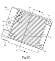
- the main circuit board 12 when installed rests on a ledge 46 above the auxiliary circuit board, as illustrated in FIG. 2C.
- the ledge 46 is formed by a lateral offset in the housing walls 22, 24, 26, 28 and extends around the inner periphery of the housing 10 as shown in FIG. 2A.
- connector pins molded into a pair of connector blocks 48a, 48b are provided by connector pins molded into a pair of connector blocks 48a, 48b.
- the connector blocks 48a, 48b are preferably insert-molded in the housing 10 and are disposed adjacent the housing wall 28.
- the connector block 48a supports both L-shaped connector pins 50 (only two of which are shown) and J-shaped connector pins 52 (only one of which is shown).
- the connector pins of connector block 48b are all L-shaped.
- the L-shaped connector pins 50 of connector blocks 48a, 48b protrude horizontally through the housing wall 28 and vertically through respective connector block surfaces 54, 56 that lie in the same plane as the ledge 46 that supports main circuit board 12.
- the J-shaped connector pins 52 of connector block 48a protrude vertically through the connector block surface 54 and a connector block surface 58 that lies in the same plane as the ledges 36 that support auxiliary circuit board 14.
- the terminal portions of the L-shaped connector pins 50 that protrude horizontally through the housing wall 28 are shrouded by connector headers 60a, 60b of housing 10.
- the terminal portions of the J-shaped connector pins 52 that protrude vertically through the connector block surface 58 electrically interconnect with plated through-holes formed in the auxiliary circuit board 14.
- the terminal portions of the L-shaped and J-shaped connector pins 50, 52 that protrude vertically through the connector block surfaces 54, 56 electrically interconnect with plated through-holes formed in the main circuit board 12.
- the terminal portions of the connector pins 50, 52 that protrude vertically through the connector block surfaces 54, 56, 58 are compliant and yield resiliently when passing through the circuit board through-holes so that soldered connections are not required.
- the main and auxiliary circuit boards 12, 14 are both secured the within the housing 10 by the application of a potting material 70 such as polyurethane to the exposed face 62 of main circuit board 12.
- the potting material 70 is applied in a single step following installation of the main and auxiliary circuit boards 12, 14 as described above.
- the main circuit board 12 is provided with a set of apertures or through-holes 64 in a portion of the circuit board that overlies the auxiliary circuit board 14. Potting material 70 deposited on the exposed face 62 of the main circuit board 12 floods a volume bounded by the exposed face 62 and portions of the housing side walls 22, 24, 26, 28 that extend above main circuit board 12.
- the potting material 70 adheres to the main circuit board 14 and the housing side walls 22, 24, 26, 28 to structurally bond the main circuit board 12 to the housing 10.
- the potting material 70 is sufficiently thin in its uncured state that it additionally flows into the apertures 64 in the main circuit board 12, forming plugs of cured potting material 70a that bridge the gap between the main and auxiliary circuit boards 12, 14 beneath the apertures 64 as shown in FIG. 3.
- the potting material plugs 70a structurally bond the auxiliary circuit board 14 to the main circuit board 12 (and hence, to housing 10), and vertically retain the auxiliary circuit board 14 on the ledge 36.
- the layer of cured potting material 70b remaining on the exposed face 62 of main circuit board 12 serves to environmentally seal the module.
- the present invention provides a sealed electronic module and manufacturing method with fastenerless support of a main circuit board and at least one auxiliary circuit board with a single application of potting material to the exposed face of the main circuit board.
- the housing 10 may have a shape other than rectangular, there may be more than one auxiliary circuit board, the number of potting material bridges may be different than illustrated, and so forth. Accordingly, it is intended that the invention not be limited to the disclosed embodiment, but that it have the full scope permitted by the language of the following claims.
Landscapes
- Engineering & Computer Science (AREA)
- Microelectronics & Electronic Packaging (AREA)
- Combinations Of Printed Boards (AREA)
- Casings For Electric Apparatus (AREA)
Abstract
Description
- The present invention relates to an electronic module including multiple circuit boards disposed in a housing that is sealed with potting material, and more particularly to an arrangement for using the potting material to secure the circuit boards in the housing.
- In the manufacture of an electronic module, one or more circuit boards populated with electronic components are inserted into a plastic or metal housing that is open on one end. In a typical application, the circuit boards are supported on one or more internal posts or flanges formed in the housing, fasteners are used to rigidly affix the circuit boards to the supports, and a sealed cover is secured to the housing to seal the module. In an alternative approach described in the
U.S. Patent No. 5,703,754 to Hinze , a housing for a single circuit board is provided with an interior ledge that supports the margin of the circuit board, and the circuit board is inserted into the housing with the components facing downward so that potting material can be applied to the exposed face of the circuit board to both affix the circuit board to the housing and environmentally seal the module. While the approach disclosed by Hinze is advantageous because it eliminates the circuit board and housing cover fasteners, it does not address modules having more than one circuit board. Accordingly, what is needed is an electronic module that is sealed with potting material and configured to receive and secure two or more circuit boards without fasteners. - The present invention is directed to a sealed electronic module and manufacturing method including a housing having an open end, a main circuit board and at least one auxiliary circuit board, where the main and auxiliary circuit boards are both secured in the housing without fasteners by a potting material that is applied to the exposed face of the main circuit board. The main circuit board is peripherally supported by a housing ledge, and the auxiliary circuit board is disposed inboard of the main circuit board. A controlled amount of the potting material applied to the exposed face of the main circuit board flows through one or more strategically placed apertures in the main circuit board, forming one or more bridges or plugs of potting material between the main circuit board and the underlying surface of the auxiliary circuit board so that potting material applied in a single step secures both main and auxiliary circuit boards in the housing while environmentally sealing the electronic module. In applications where the housing is formed of plastic or other nonconductive material, electrical interconnections among the main and auxiliary circuit boards and a connector of the electronic module are established by compliant conductor pins that protrude from housing surfaces that provide peripheral support for the main and auxiliary circuit boards.
-
- FIG. 1 is an exploded isometric view of an electronic module according to this invention, including a housing, a main circuit board and an auxiliary circuit board;
- FIG. 2A is an overhead isometric view of the housing of FIG. 1 prior to installation of the main and auxiliary circuit boards;
- FIG. 2B is an overhead isometric view of the housing of FIG. 1 following installation of auxiliary circuit board, but prior to installation of the main circuit board;
- FIG. 2C is an overhead isometric view of the housing of FIG. 1 following installation of the main and auxiliary circuit boards;
- FIG. 3 is a cross-sectional view of the completed electronic module of this invention, taken along lines A-A of FIG. 2C; and
- FIG. 4 is an isometric cross-sectional view of the housing of FIG. 1 prior to installation of the main and auxiliary circuit boards, showing connector pins electrically interconnecting the main and auxiliary circuit boards.
- Referring to FIG. 1, the
reference numerals auxiliary circuit boards capacitors 16 andaccelerometer 17, and each board is oriented so that its major components face downward - i.e., toward thebottom 20 ofhousing 10. In general, the main andauxiliary circuit boards housing 10 in the order depicted in FIG. 1, and then sealed in place with a potting material such as polyurethane applied to the exposed face of themain circuit board 12. - Referring additionally to FIGS. 2A-2C, the
housing 10 includesside walls bottom 20 and a set ofintegral mounting tabs housing 10 is open-ended as shown to receive the populatedcircuit boards auxiliary circuit board 14 is installed inboard of themain circuit board 12 as indicated in FIG. 1, and rests on a set of four L-shaped ledges 36 formed by four stepped L-shapedinner housing walls main circuit board 12 when installed rests on aledge 46 above the auxiliary circuit board, as illustrated in FIG. 2C. Theledge 46 is formed by a lateral offset in thehousing walls housing 10 as shown in FIG. 2A. - Electrical connections among the main and
auxiliary circuit boards connector blocks housing 10 and are disposed adjacent thehousing wall 28. Referring to FIG. 4, theconnector block 48a supports both L-shaped connector pins 50 (only two of which are shown) and J-shaped connector pins 52 (only one of which is shown). Although not illustrated in FIG. 4, the connector pins ofconnector block 48b are all L-shaped. The L-shaped connector pins 50 of connector blocks 48a, 48b protrude horizontally through thehousing wall 28 and vertically through respectiveconnector block surfaces ledge 46 that supportsmain circuit board 12. The J-shaped connector pins 52 ofconnector block 48a protrude vertically through theconnector block surface 54 and aconnector block surface 58 that lies in the same plane as theledges 36 that supportauxiliary circuit board 14. The terminal portions of the L-shaped connector pins 50 that protrude horizontally through thehousing wall 28 are shrouded byconnector headers housing 10. The terminal portions of the J-shaped connector pins 52 that protrude vertically through theconnector block surface 58 electrically interconnect with plated through-holes formed in theauxiliary circuit board 14. And the terminal portions of the L-shaped and J-shaped connector pins connector block surfaces main circuit board 12. Preferably, the terminal portions of theconnector pins connector block surfaces - According to the invention, the main and
auxiliary circuit boards housing 10 by the application of apotting material 70 such as polyurethane to the exposedface 62 ofmain circuit board 12. Thepotting material 70 is applied in a single step following installation of the main andauxiliary circuit boards main circuit board 12 is provided with a set of apertures or through-holes 64 in a portion of the circuit board that overlies theauxiliary circuit board 14.Potting material 70 deposited on the exposedface 62 of themain circuit board 12 floods a volume bounded by the exposedface 62 and portions of thehousing side walls main circuit board 12. When cured, thepotting material 70 adheres to themain circuit board 14 and thehousing side walls main circuit board 12 to thehousing 10. Thepotting material 70 is sufficiently thin in its uncured state that it additionally flows into theapertures 64 in themain circuit board 12, forming plugs of curedpotting material 70a that bridge the gap between the main andauxiliary circuit boards apertures 64 as shown in FIG. 3. The potting material plugs 70a structurally bond theauxiliary circuit board 14 to the main circuit board 12 (and hence, to housing 10), and vertically retain theauxiliary circuit board 14 on theledge 36. Additionally, the layer of curedpotting material 70b remaining on the exposedface 62 ofmain circuit board 12 serves to environmentally seal the module. - In summary, the present invention provides a sealed electronic module and manufacturing method with fastenerless support of a main circuit board and at least one auxiliary circuit board with a single application of potting material to the exposed face of the main circuit board. While the present invention has been described in reference to the illustrated embodiment, it will be recognized that various modifications will occur to those skilled in the art. For example, the
housing 10 may have a shape other than rectangular, there may be more than one auxiliary circuit board, the number of potting material bridges may be different than illustrated, and so forth. Accordingly, it is intended that the invention not be limited to the disclosed embodiment, but that it have the full scope permitted by the language of the following claims.
Claims (10)
- A sealed and fastenerless electronic module comprising:first and second circuit boards (14, 12);a housing (10) having an open end through which said first and second circuit boards (14, 12) are inserted, where said first circuit board (14) is disposed inboard of said second circuit board (12), and said second circuit board (12) closes the open end of said housing (10); anda quantity of potting material (70) sealing said housing (10) and securing said first and second circuit boards (14, 12) within said housing (10), including a layer of potting material (70b) filling a volume defined by said housing (10) and an outboard face (62) of said second circuit board (12), and one or more plugs of potting material (70a) extending through one or more apertures (64) formed in said second circuit board (12) and bridging a gap between said first and second circuit boards (14, 12).
- The sealed electronic module of claim 1, further comprising:a first set of connector pins (50) electrically coupling said second circuit board (12) to a connector (60a) of said housing (10); anda second set of connector pins (52) electrically coupling said first circuit board (14) to said second circuit board (12).
- The sealed electronic module of claim 1, further comprising:an upper support surface (54) for supporting a margin of said second circuit board (12) within said housing (10); anda set of connector pins (50, 52) protruding through a portion of said upper support surface (54) and said second circuit board (12).
- The sealed electronic module of claim 1, further comprising:a lower support surface (58) for supporting a margin of said first circuit board (14) within said housing (10); anda set of connector pins (52) protruding through a portion of said lower support surface (58) and said first circuit board (14).
- The sealed electronic module of claim 1, further comprising:a lower support surface (58) for supporting a margin of said first circuit board (14) and an upper support surface (54) for supporting a margin of said second circuit board (12); anda set of connector pins (52) protruding at one end through said lower support surface (58) for electrical connection with said first circuit board (14), and at the other end through said upper support surface (54) for electrical connection with said second circuit board (12).
- A method of manufacturing a sealed and fastenerless electronic module comprising the steps of:providing a housing (10) having an open end and lower and upper support surfaces (58, 54) for supporting first and second circuit boards (14, 12), respectively, where said upper support surface (54, 46) is an interior ledge that bounds the open end of said housing (10);placing said first circuit board (14) on the lower support surface (58) of said housing (10);placing the second circuit board (12) on the upper support surface (54) of said housing (10) to close the open end of said housing (10); anddispensing a quantity of potting material (70) on an exposed face (62) of said second circuit board (12) so that a first portion of said potting material (70b) covers said exposed face (62) to thereby seal said housing (10) and secure said second circuit board (12) in said housing (10), and a second portion of said potting material (70a) flows through one or more apertures (64) formed in said second circuit board (12) to form one or more bridges of potting material (70a) between said second circuit board (12) and an underlying surface of said first circuit board (14) to thereby secure said first circuit board (14) in said housing (10).
- The method of Claim 6, including the steps of:providing a set of electrical connector pins (50) that protrude through said upper support surface (54) for electrically coupling said second circuit board (14) to a connector (60a) of said housing (10); andinserting terminal portions of said connector pins (50) through openings formed in said second circuit board (14) when said second circuit board (14) is placed on said upper support surface (54).
- The method of Claim 7, where said terminal portions of said connector pins (50) yield compliantly when inserted into the openings of said second circuit board (14).
- The method of Claim 6, including the steps of:providing a set of electrical connector pins (52) that protrude through both said lower support surface (58) and said upper support surface (54) for electrically connecting said first circuit board (14) to said second circuit board (12);inserting first terminal portions of said connector pins (50) through openings in said first circuit board (14) when said first circuit board (14) is placed on said lower support surface (58); andinserting second terminal portions of said connector pins (52) through openings in said second circuit board (12) when said second circuit board (12) is placed on said upper support surface (54).
- The method of Claim 9, where said first and second terminal portions of said connector pins (52) yield compliantly when inserted into the openings of said first and second circuit boards (14, 12).
Applications Claiming Priority (1)
| Application Number | Priority Date | Filing Date | Title |
|---|---|---|---|
| US11/157,007 US20060286845A1 (en) | 2005-06-20 | 2005-06-20 | Sealed fastenerless multi-board electronic module and method of manufacture |
Publications (2)
| Publication Number | Publication Date |
|---|---|
| EP1737286A2 true EP1737286A2 (en) | 2006-12-27 |
| EP1737286A3 EP1737286A3 (en) | 2009-01-21 |
Family
ID=37072570
Family Applications (1)
| Application Number | Title | Priority Date | Filing Date |
|---|---|---|---|
| EP06076169A Withdrawn EP1737286A3 (en) | 2005-06-20 | 2006-06-06 | Sealed fastenerless multi-board electronic module and method of manufacture |
Country Status (2)
| Country | Link |
|---|---|
| US (1) | US20060286845A1 (en) |
| EP (1) | EP1737286A3 (en) |
Cited By (7)
| Publication number | Priority date | Publication date | Assignee | Title |
|---|---|---|---|---|
| EP2031947A1 (en) * | 2007-08-30 | 2009-03-04 | Delphi Technologies, Inc. | Electronic assembly having housing with embedded conductor connecting electrical component |
| EP2040527A1 (en) | 2007-09-21 | 2009-03-25 | Continental Automotive GmbH | Electronics housing |
| EP1996000A3 (en) * | 2007-05-24 | 2009-07-22 | Delphi Technologies, Inc. | Stand-off mounting apparatus for discrete electrical components |
| FR2933267A1 (en) * | 2008-06-27 | 2010-01-01 | Thales Sa | Electronic cabinet for receiving electronic components of airplane, has enclosure incorporating electronic board that is surrounded by aeraulics circuit, with wall incorporating motherboard, to circulate refrigerant to interior of cabinet |
| EP2775809A3 (en) * | 2013-03-05 | 2017-08-02 | WABCO GmbH | Housing for accommodating a printed circuit board with at least one connector interface, electronic module with such a housing, motor vehicle with the same and method for producing such a housing or electronic module |
| CN110235532A (en) * | 2017-01-25 | 2019-09-13 | 罗伯特·博世有限公司 | For being mechanically connected and the method for arranging electronic structural detail |
| EP3897084A1 (en) * | 2020-04-16 | 2021-10-20 | Pegatron Corporation | Housing and electronic device using same |
Families Citing this family (7)
| Publication number | Priority date | Publication date | Assignee | Title |
|---|---|---|---|---|
| EP2064704A1 (en) * | 2006-09-20 | 2009-06-03 | John W Hannay & Company Limited | Methods and apparatus for creation, distribution and presentation of polymorphic media |
| JP2013093372A (en) * | 2011-10-24 | 2013-05-16 | Keihin Corp | Electronic control device |
| US9368905B2 (en) | 2014-07-22 | 2016-06-14 | Cooper Technologies Company | Potting compound chamber designs for electrical connectors |
| WO2017079416A1 (en) | 2015-11-06 | 2017-05-11 | Cooper Technologies Company | Potting compound chamber designs for electrical connectors |
| JP2017098332A (en) * | 2015-11-19 | 2017-06-01 | 株式会社ジェイテクト | Electronic circuit equipment |
| EP3361842B1 (en) | 2017-02-10 | 2021-04-07 | W & H Dentalwerk Bürmoos GmbH | Medical regulating or controlling device |
| US11088066B2 (en) * | 2018-03-19 | 2021-08-10 | Tactotek Oy | Multilayer structure and related method of manufacture for electronics |
Family Cites Families (18)
| Publication number | Priority date | Publication date | Assignee | Title |
|---|---|---|---|---|
| DE2305484C3 (en) * | 1973-02-05 | 1978-08-24 | Siemens Ag, 1000 Berlin Und 8000 Muenchen | Excitation device for a DC alternator |
| US4600969A (en) * | 1984-07-06 | 1986-07-15 | Hendrickson Max S | Protective apparatus for encapsulating electrical circuits |
| JPH02170597A (en) * | 1988-12-23 | 1990-07-02 | Mazda Motor Corp | On-vehicle control unit structure |
| JP2705368B2 (en) * | 1991-05-31 | 1998-01-28 | 株式会社デンソー | Electronic equipment |
| JP2936855B2 (en) * | 1991-12-26 | 1999-08-23 | 富士電機株式会社 | Power semiconductor device |
| JP2956363B2 (en) * | 1992-07-24 | 1999-10-04 | 富士電機株式会社 | Power semiconductor device |
| US5381304A (en) * | 1993-06-11 | 1995-01-10 | Honeywell Inc. | Reworkable encapsulated electronic assembly and method of making same |
| JPH07297575A (en) * | 1994-04-21 | 1995-11-10 | Mitsubishi Electric Corp | Power module equipment |
| EP0722200B1 (en) * | 1995-01-10 | 2001-03-21 | Sumitomo Wiring Systems, Ltd. | Junction box |
| US5703754A (en) * | 1996-02-26 | 1997-12-30 | Delco Electronics Corporation | Fastenerless sealed electronic module |
| US6012223A (en) * | 1998-07-31 | 2000-01-11 | Delco Electronics Corp. | Process for structurally securing stick-leaded components to a circuit board |
| JP2000165068A (en) * | 1998-11-25 | 2000-06-16 | Alps Electric Co Ltd | Mounting structure for printed board |
| US6245995B1 (en) * | 1999-12-20 | 2001-06-12 | General Electric Company | Methods and apparatus for removing moisture from an enclosure |
| US6317324B1 (en) * | 2000-02-01 | 2001-11-13 | Shiaw-Jong Steve Chen | Encapsulated power supply with a high thermal conductivity molded insert |
| DE10121776B4 (en) * | 2001-05-04 | 2006-10-19 | Sick Ag | sensor |
| US7336500B1 (en) * | 2004-09-03 | 2008-02-26 | Altera Corporation | Method and apparatus for encapsulating a printed circuit board |
| US7209360B1 (en) * | 2005-10-28 | 2007-04-24 | Lear Corporation | Leak-tight system for boxes containing electrical and electronic components |
| TWI402952B (en) * | 2007-09-27 | 2013-07-21 | 三洋電機股份有限公司 | Circuit device and method of manufacturing same |
-
2005
- 2005-06-20 US US11/157,007 patent/US20060286845A1/en not_active Abandoned
-
2006
- 2006-06-06 EP EP06076169A patent/EP1737286A3/en not_active Withdrawn
Cited By (12)
| Publication number | Priority date | Publication date | Assignee | Title |
|---|---|---|---|---|
| EP1996000A3 (en) * | 2007-05-24 | 2009-07-22 | Delphi Technologies, Inc. | Stand-off mounting apparatus for discrete electrical components |
| US7791901B2 (en) | 2007-05-24 | 2010-09-07 | Delphi Technologies, Inc. | Stand-off mounting apparatus for discrete electrical components |
| EP2031947A1 (en) * | 2007-08-30 | 2009-03-04 | Delphi Technologies, Inc. | Electronic assembly having housing with embedded conductor connecting electrical component |
| EP2040527A1 (en) | 2007-09-21 | 2009-03-25 | Continental Automotive GmbH | Electronics housing |
| FR2933267A1 (en) * | 2008-06-27 | 2010-01-01 | Thales Sa | Electronic cabinet for receiving electronic components of airplane, has enclosure incorporating electronic board that is surrounded by aeraulics circuit, with wall incorporating motherboard, to circulate refrigerant to interior of cabinet |
| EP2775809A3 (en) * | 2013-03-05 | 2017-08-02 | WABCO GmbH | Housing for accommodating a printed circuit board with at least one connector interface, electronic module with such a housing, motor vehicle with the same and method for producing such a housing or electronic module |
| CN110235532A (en) * | 2017-01-25 | 2019-09-13 | 罗伯特·博世有限公司 | For being mechanically connected and the method for arranging electronic structural detail |
| CN110235532B (en) * | 2017-01-25 | 2022-07-12 | 罗伯特·博世有限公司 | Method for mechanically connecting and arranging electronic components |
| EP3897084A1 (en) * | 2020-04-16 | 2021-10-20 | Pegatron Corporation | Housing and electronic device using same |
| CN113543540A (en) * | 2020-04-16 | 2021-10-22 | 和硕联合科技股份有限公司 | Shell and electronic device using same |
| US11291132B2 (en) | 2020-04-16 | 2022-03-29 | Pegatron Corporation | Housing and electronic device using same |
| CN113543540B (en) * | 2020-04-16 | 2023-03-21 | 和硕联合科技股份有限公司 | Shell and electronic device using same |
Also Published As
| Publication number | Publication date |
|---|---|
| US20060286845A1 (en) | 2006-12-21 |
| EP1737286A3 (en) | 2009-01-21 |
Similar Documents
| Publication | Publication Date | Title |
|---|---|---|
| US7146721B2 (en) | Method of manufacturing a sealed electronic module | |
| EP1581036A2 (en) | Method of manufacturing a sealed electronic module | |
| EP1737286A2 (en) | Sealed fastenerless multi-board electronic module and method of manufacture | |
| US5452948A (en) | Apparatus and method for electronically controlled hydraulic actuator | |
| US5999067A (en) | High performance RF/microwave filters for surface mount technology with a shielding metal bracket | |
| US9258918B2 (en) | Module for integrated control electronics having simplified design | |
| US6283769B1 (en) | Electric connecting box | |
| AU622596B2 (en) | Connector with means for securing to a substrate | |
| US6477052B1 (en) | Multiple layer thin flexible circuit board | |
| US10834833B1 (en) | Sealed ECU module housing with comb support | |
| US6547597B2 (en) | Apparatus and method for incorporating surface mount components into connectors | |
| US8139377B2 (en) | IC device and method of manufacturing the same | |
| CN116937963A (en) | EMC filter assembly, inverter and assembly method of EMC filter assembly | |
| US6919221B2 (en) | Electronic module having a plastic housing with conductive tracks and method of its production | |
| FI115110B (en) | Microcircuit boards and process for making and designing and mounting microcircuits | |
| DE102007044394A1 (en) | Module for integrated control electronics with simplified design | |
| EP2031947A1 (en) | Electronic assembly having housing with embedded conductor connecting electrical component | |
| CN1955454B (en) | Electronic circuit unit | |
| US6939147B2 (en) | Junction box and soldering method for printed circuit board of the junction box | |
| CN222147875U (en) | Circuit board, motor base and motor | |
| CN222763236U (en) | Vehicle-mounted connector | |
| EP4593208A1 (en) | Connector | |
| JP2738317B2 (en) | connector | |
| RU2191494C2 (en) | Radio-electronic unit | |
| CN1110445A (en) | Electronic product components that are integrated and easy to dissipate heat |
Legal Events
| Date | Code | Title | Description |
|---|---|---|---|
| PUAI | Public reference made under article 153(3) epc to a published international application that has entered the european phase |
Free format text: ORIGINAL CODE: 0009012 |
|
| AK | Designated contracting states |
Kind code of ref document: A2 Designated state(s): AT BE BG CH CY CZ DE DK EE ES FI FR GB GR HU IE IS IT LI LT LU LV MC NL PL PT RO SE SI SK TR |
|
| AX | Request for extension of the european patent |
Extension state: AL BA HR MK YU |
|
| PUAL | Search report despatched |
Free format text: ORIGINAL CODE: 0009013 |
|
| AK | Designated contracting states |
Kind code of ref document: A3 Designated state(s): AT BE BG CH CY CZ DE DK EE ES FI FR GB GR HU IE IS IT LI LT LU LV MC NL PL PT RO SE SI SK TR |
|
| AX | Request for extension of the european patent |
Extension state: AL BA HR MK RS |
|
| RIC1 | Information provided on ipc code assigned before grant |
Ipc: H05K 5/00 20060101ALI20081218BHEP Ipc: H05K 5/06 20060101ALI20081218BHEP Ipc: H05K 7/14 20060101ALI20081218BHEP Ipc: B60R 16/023 20060101AFI20081218BHEP |
|
| 17P | Request for examination filed |
Effective date: 20090721 |
|
| AKX | Designation fees paid |
Designated state(s): AT BE BG CH CY CZ DE DK EE ES FI FR GB GR HU IE IS IT LI LT LU LV MC NL PL PT RO SE SI SK TR |
|
| GRAP | Despatch of communication of intention to grant a patent |
Free format text: ORIGINAL CODE: EPIDOSNIGR1 |
|
| STAA | Information on the status of an ep patent application or granted ep patent |
Free format text: STATUS: THE APPLICATION IS DEEMED TO BE WITHDRAWN |
|
| 18D | Application deemed to be withdrawn |
Effective date: 20110102 |