EP1737207A1 - System for selecting a format for control data in an imaging device - Google Patents
System for selecting a format for control data in an imaging device Download PDFInfo
- Publication number
- EP1737207A1 EP1737207A1 EP06114476A EP06114476A EP1737207A1 EP 1737207 A1 EP1737207 A1 EP 1737207A1 EP 06114476 A EP06114476 A EP 06114476A EP 06114476 A EP06114476 A EP 06114476A EP 1737207 A1 EP1737207 A1 EP 1737207A1
- Authority
- EP
- European Patent Office
- Prior art keywords
- photosensors
- control data
- subset
- data format
- subsystem
- Prior art date
- Legal status (The legal status is an assumption and is not a legal conclusion. Google has not performed a legal analysis and makes no representation as to the accuracy of the status listed.)
- Granted
Links
- 238000003384 imaging method Methods 0.000 title claims abstract description 7
- 230000010354 integration Effects 0.000 claims abstract description 38
- 230000008859 change Effects 0.000 claims description 7
- 238000010586 diagram Methods 0.000 description 7
- 238000003491 array Methods 0.000 description 5
- 238000000034 method Methods 0.000 description 5
- XUIMIQQOPSSXEZ-UHFFFAOYSA-N Silicon Chemical group [Si] XUIMIQQOPSSXEZ-UHFFFAOYSA-N 0.000 description 3
- 230000000694 effects Effects 0.000 description 3
- 238000002955 isolation Methods 0.000 description 2
- 230000008569 process Effects 0.000 description 2
- 230000009471 action Effects 0.000 description 1
- 230000000903 blocking effect Effects 0.000 description 1
- 238000006243 chemical reaction Methods 0.000 description 1
- 239000003086 colorant Substances 0.000 description 1
- 230000000052 comparative effect Effects 0.000 description 1
- 238000010276 construction Methods 0.000 description 1
- 230000003993 interaction Effects 0.000 description 1
- 230000003287 optical effect Effects 0.000 description 1
- 230000002829 reductive effect Effects 0.000 description 1
- 230000004044 response Effects 0.000 description 1
- 229910052710 silicon Inorganic materials 0.000 description 1
- 239000010703 silicon Substances 0.000 description 1
- 238000001429 visible spectrum Methods 0.000 description 1
Images



Classifications
-
- H—ELECTRICITY
- H04—ELECTRIC COMMUNICATION TECHNIQUE
- H04N—PICTORIAL COMMUNICATION, e.g. TELEVISION
- H04N1/00—Scanning, transmission or reproduction of documents or the like, e.g. facsimile transmission; Details thereof
- H04N1/40—Picture signal circuits
- H04N1/40056—Circuits for driving or energising particular reading heads or original illumination means
-
- H—ELECTRICITY
- H04—ELECTRIC COMMUNICATION TECHNIQUE
- H04N—PICTORIAL COMMUNICATION, e.g. TELEVISION
- H04N1/00—Scanning, transmission or reproduction of documents or the like, e.g. facsimile transmission; Details thereof
- H04N1/00912—Arrangements for controlling a still picture apparatus or components thereof not otherwise provided for
- H04N1/00933—Timing control or synchronising
-
- H—ELECTRICITY
- H04—ELECTRIC COMMUNICATION TECHNIQUE
- H04N—PICTORIAL COMMUNICATION, e.g. TELEVISION
- H04N1/00—Scanning, transmission or reproduction of documents or the like, e.g. facsimile transmission; Details thereof
- H04N1/04—Scanning arrangements, i.e. arrangements for the displacement of active reading or reproducing elements relative to the original or reproducing medium, or vice versa
- H04N1/19—Scanning arrangements, i.e. arrangements for the displacement of active reading or reproducing elements relative to the original or reproducing medium, or vice versa using multi-element arrays
Definitions
- the present disclosure relates to image scanning arrays, as in a digital copier or digital camera.
- Image sensor arrays typically comprise a linear array of photosensors which raster scan an image-bearing document and convert the microscopic image areas viewed by each photosensor to video image signals. Following an integration period, the image signal charges formed on the photosensors are amplified and transferred as analog video signals to a common output line or bus through successively actuated multiplexing transistors.
- one embodiment includes an array of photosensors of a width comparable to the width of a page being scanned, to permit imaging generally without the use of reductive optics.
- relatively large silicon structures must be used to define the large number of photosensors.
- an array is made of twenty silicon chips, butted end-to-end, each chip having 248 active photosensors spaced at 400 photosensors per inch.
- the chips which are butted to form the array are formed in a silicon wafer, which is then "diced” into a number of chips, which are individually tested and then arranged into a bar shape.
- the present disclosure relates to a chip configuration that can be readily adapted for use in a larger system or apparatus, taking into account a given format of control data by which the larger system controls the chips.
- an imaging apparatus comprising at least one controllable subset of photosensors.
- a first subsystem operates the subset of photosensors according to a first control data format
- second subsystem for operating the subset of photosensors according to a second control data format.
- an imaging apparatus comprising at least a first subset of photosensors.
- a first subsystem operates the first subset of photosensors according to a first control data format, the first control data format including a signal being in a predetermined state for substantially a duration of a desired integration period for the subset of photosensors.
- a second subsystem operates the first subset of photosensors according to a second control data format, the second control data format including a signal causing the beginning or ending of an integration period of the subset of photosensors.
- a selector selects one of the first control data format and the second control data format.
- Figure 1 is a plan view of a portion of a "full-width-array" input scanner as would be used in office equipment such as a digital copier.
- Figure 2 is a plan view of a photosensor chip in isolation.
- Figure 3 is a simplified timing diagram showing a typical operation of a chip for one cycle of operation according one type of control data format.
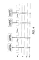
- Figure 4 is a simplified timing diagram showing a typical operation of a chip for one cycle of operation according to another type of control data format.
- Figure 5 is a simplified block diagram of a control system of a photosensor chip, by which the control data format to operate the chip can be selected.
- FIG. 1 is a plan view of a portion of a "full-width-array" input scanner as would be used in office equipment such as a digital copier.
- a set of photosensor chips, each indicated as 10 is arranged on a circuit board 100.
- Each chip 10 includes a set of photosensors, as will be described below.
- the chips 10 on board 100 form one or more linear arrays of photosensors that extend a length comparable to the width of an image-bearing sheet such as S effectively moving in a process direction P.
- the sheet S can move relative to the board 100 by being placed on a platen (not shown) relative to which the board 100 moves; or the sheet S can be fed through a document handler (not shown).
- a series of small areas on the sheet S reflect light (from a source, not shown) into photosensors on the chips 10.
- the chips 10 receive the reflected light from sheet S and output image signals for subsequent recording and processing.
- FIG. 2 shows a photosensor chip 10 in isolation.
- each chip 10 includes four linear arrays, or rows, of photosensors, labeled 20M (for monochrome, or white), 20R (for red), 20G (for green) and 20B (for blue).
- Each array is provided with a translucent filter (not shown) that causes the array to be sensitive to a particular color or range of wavelength.
- the monochrome array 20M is sensitive to light throughout the visible spectrum, and is useful when scanning images for monochrome-only image data, as would be useful, for example, in a monochrome copier or facsimile machine, or for optical character scanning.
- the photosensors may also be provided with other types of filters, such as for infrared blocking.
- each photosensor in a subset undergoes different changes in its "integration state.”
- the photosensor enters an "integration period,” in which any light falling on the photosensor is used to accumulate a charge on the photosensor.
- another predetermined potential is placed on the photosensor.
- the accumulated charge which relates generally to the intensity of light having fallen on the photosensor during the integration period, is transferred off the photosensor in a known manner.
- "changing the integration state" of a photosensor includes any instance in which a potential or charge is placed on or is associated with a photosensor, to begin or end an integration period.
- the controller 26 (which need not be a discrete portion of the chip 10, as shown in the embodiment, but rather may reflect capabilities that reside in various places on or off chip 10) accepts a set of control lines, generally indicated as 30, each carrying a specific type of signal, from a control system off the chip.
- the control data entering on lines 30 must be in a predetermined format.
- Figures 3 and 4 are comparative, simplified diagrams of typical control data formats for operating subsets of photosensors on a chip over the recording of one or more scanlines.
- One possible type of format for controlling the photosensors is characterized by a signal entering the chip, the signal being in a predetermined state for substantially a duration of a desired integration period for a selected subset of photosensors.
- a signal entering the chip the signal being in a predetermined state for substantially a duration of a desired integration period for a selected subset of photosensors.
- FIG 3 there is a simplified diagram of how signals ⁇ FR, ⁇ FG, ⁇ FB (entered on one or more lines such as 30) control the integration times of the individual rows of photosensors. The overall operation is described in more detail in, for example, US Patent 5,519,514 mentioned above.
- the integration period for the red row 20R corresponds to the relevant signal ⁇ FR being high on a line 30: when ⁇ FR is high, the red row of photosensors 20R undergoes its integration period (in effect, "the shutter is open"), and when ⁇ FR is low, integration is not occurring (in effect, "the shutter is closed”).
- the same principle applies, as can be seen, to other rows and corresponding signals (the operation of the monochrome row 20M is typically optional depending on a desired scanning operation).
- Another possible format for controlling the photosensors includes a signal (such as, but not limited to, a pulse, or a change in state) causing the beginning or ending of the integration period of a subset of photosensors.
- a signal such as, but not limited to, a pulse, or a change in state
- a chip accepts an integration control signal IC on one of the control lines such as 30.
- the integration control signal IC causes the photosensors in a selected row or other subset to have a change in integration state.
- the photosensors When a subset of photosensors such as row 30R receives an IC signal, the photosensors simply change their integration state from whatever the state happens to be at the time: the salient feature is that the IC signal changes the integration state of a subset of photosensors, as opposed to defining the duration of the integration state, as with the above-described method.
- the row select signals RS1 and RS0 which can be loaded through other lines 30, represent a two-bit parallel code identifying the subset to change in integration state in response to the next IC signal.
- the two-bit parallel lines can thus select, over time, one of the four rows of photosensors 20M, 20R, 20G, 20B in the chip of Figure 2, to have its integration state changed with the next IC signal.
- the pixel clock ⁇ S is typically a constantly-running square wave of a predetermined frequency.
- the larger system such as a digital scanner or digital copier
- the larger system may use one or another type of control data format to control the operation of the chips 10. It is desirable to provide chips 10 of a design that enables control with either control data format, so one basic chip design can be installed in machines with either type of control data format.
- FIG. 5 is a simplified block diagram of a system within a control system 26 of a chip 10 by which the control data format to operate the chip can be selected.
- the input lines 30 onto chip 10 branch off to both a "duration" based integration control subsystem 40 and a "change integration state” based integration control subsystem 42: as such, the inputs into subsystem 40 are ⁇ FR, ⁇ FG, ⁇ FB as seen in Figure 3, and the inputs into subsystem 42 are IC, RS0, and RS1 as seen in Figure 4. Regardless of which type of control signals are used in the larger apparatus, these control signals are entered on input lines 30 and, depending on the type, are sent to one or the other subsystem 40 or 42.
- the term "subsystem” shall mean any signal-processing entity, incorporating hardware and/or software, which processes the incoming control signals; and may or may not include, or go beyond, elements in the illustrated embodiment.
- the subsystems 40 and 42 each accept incoming control signals of a given type and, in the present embodiment, in turn output control data for starting and stopping the integration periods in the various subsets of photosensors 20M, 20R, 20G, 20B, as can be seen by the output labels in Figure 5.
- the conversions of data within each subsystem 40, 42 may be carried out in hardware or software.
- the converted data from either subsystem 40 or 42 is then multiplexed in a multiplexer 44.
- the output of multiplexer 44 is signals that directly affect the integration states of the photosensors in each subset.
- Another input to multiplexer 44 is one or more selection lines, here indicated as Sel_T and Sel_S. These selection lines tell the multiplexer 44 which input (from either subsystem 40 or 42) to use in its output.
- Sample gating arrangement 46 is representative of the interaction of the various signals for each combination xY of inputs to multiplexer 44.
- the aspects of the multiplexer 44 responsive to selection lines Sel_T and Sel_S can be considered a example of a "selector" for selecting which type of control data format will be processed by chip 10.
- chips 10 of a single basic design are installed on a board 100 (as shown in Figure 1) that is disposed within a larger apparatus such as a scanner or digital copier.
- the larger apparatus will use one control data format, either "duration” based or "change integration state” based.
- By setting the control lines Sel_T and Sel_S of each chip 10, typically (but not necessarily) at the time of construction of the larger apparatus one can adapt the chips to accept the control data format of the larger apparatus.
- Chips 10 can thus be installed in a larger system or apparatus using either type of control data format.
- Figure 5 shows a common set of input lines 30 going into subsystems 40 and 42
- an alternate design could provide two separate sets of input lines, one set for each subsystem 40 and 42; in such an arrangement one subsystem could in effect be "selected" by the larger apparatus being connected only to the lines of the subsystem suitable for the apparatus' control data format.
- the present embodiment is directed toward controlling the integration times of different-filtered linear rows of photosensors
- the principle can be applied to controlling any kind of subsets of photosensors in an apparatus, such as in a two-dimensional photosensor array as would be found in a digital camera.
- the different, effectively independently-controllable subsets could be related by color (such as to alter the color balance or other output of the apparatus); or by sub-area within a the linear or two-dimensional array (in case only a portion of the array is desired to be used at a particular time).
- Photosensors of different selectable subsets could be commingled with each other within the array, such as to enable "low resolution" operation; i.e., in low resolution only an evenly-distributed subset of photosensors in the array would be read out.
- the overall system can also facilitate an array wherein one subset of photosensors are effectively provided with a longer integration or exposure time than another commingled subset: such an arrangement may be useful in improving the exposure latitude of a digital camera, such as to allow taking a long-exposure picture and a short-exposure picture simultaneously.
Landscapes
- Engineering & Computer Science (AREA)
- Multimedia (AREA)
- Signal Processing (AREA)
- Facsimile Heads (AREA)
- Transforming Light Signals Into Electric Signals (AREA)
Abstract
Description
- The present disclosure relates to image scanning arrays, as in a digital copier or digital camera.
- Image sensor arrays typically comprise a linear array of photosensors which raster scan an image-bearing document and convert the microscopic image areas viewed by each photosensor to video image signals. Following an integration period, the image signal charges formed on the photosensors are amplified and transferred as analog video signals to a common output line or bus through successively actuated multiplexing transistors.
- For high-performance image sensor arrays, one embodiment includes an array of photosensors of a width comparable to the width of a page being scanned, to permit imaging generally without the use of reductive optics. In order to provide such a "full-width" array, however, relatively large silicon structures must be used to define the large number of photosensors. In one design, an array is made of twenty silicon chips, butted end-to-end, each chip having 248 active photosensors spaced at 400 photosensors per inch. Typically, the chips which are butted to form the array are formed in a silicon wafer, which is then "diced" into a number of chips, which are individually tested and then arranged into a bar shape.
- The present disclosure relates to a chip configuration that can be readily adapted for use in a larger system or apparatus, taking into account a given format of control data by which the larger system controls the chips.
- According to one aspect, there is provided an imaging apparatus, comprising at least one controllable subset of photosensors. A first subsystem operates the subset of photosensors according to a first control data format, and second subsystem for operating the subset of photosensors according to a second control data format.
- According to another aspect, there is provided an imaging apparatus comprising at least a first subset of photosensors. A first subsystem operates the first subset of photosensors according to a first control data format, the first control data format including a signal being in a predetermined state for substantially a duration of a desired integration period for the subset of photosensors. A second subsystem operates the first subset of photosensors according to a second control data format, the second control data format including a signal causing the beginning or ending of an integration period of the subset of photosensors. A selector selects one of the first control data format and the second control data format.
- Figure 1 is a plan view of a portion of a "full-width-array" input scanner as would be used in office equipment such as a digital copier.
- Figure 2 is a plan view of a photosensor chip in isolation.
- Figure 3 is a simplified timing diagram showing a typical operation of a chip for one cycle of operation according one type of control data format.
- Figure 4 is a simplified timing diagram showing a typical operation of a chip for one cycle of operation according to another type of control data format.
- Figure 5 is a simplified block diagram of a control system of a photosensor chip, by which the control data format to operate the chip can be selected.
- Figure 1 is a plan view of a portion of a "full-width-array" input scanner as would be used in office equipment such as a digital copier. A set of photosensor chips, each indicated as 10, is arranged on a
circuit board 100. Eachchip 10 includes a set of photosensors, as will be described below. Together, thechips 10 onboard 100 form one or more linear arrays of photosensors that extend a length comparable to the width of an image-bearing sheet such as S effectively moving in a process direction P. The sheet S can move relative to theboard 100 by being placed on a platen (not shown) relative to which theboard 100 moves; or the sheet S can be fed through a document handler (not shown). As the sheet S moves pastboard 100, a series of small areas on the sheet S reflect light (from a source, not shown) into photosensors on thechips 10. Thechips 10 receive the reflected light from sheet S and output image signals for subsequent recording and processing. - Figure 2 shows a
photosensor chip 10 in isolation. In this embodiment, eachchip 10 includes four linear arrays, or rows, of photosensors, labeled 20M (for monochrome, or white), 20R (for red), 20G (for green) and 20B (for blue). Each array is provided with a translucent filter (not shown) that causes the array to be sensitive to a particular color or range of wavelength. Themonochrome array 20M is sensitive to light throughout the visible spectrum, and is useful when scanning images for monochrome-only image data, as would be useful, for example, in a monochrome copier or facsimile machine, or for optical character scanning. The photosensors may also be provided with other types of filters, such as for infrared blocking. - In the present embodiment, for each "column" (as shown in the Figure) of one photosensor of each
type output shift register 24. A general description of how multiple photosensors in a column send signals over one line to a shift register is given inUS patent 5,148,168 mentioned above. It will be evident that each photosensor of eachtype US Patent 5,519,514 mentioned above. Once a "scanline" of digital image signals is loaded intoshift register 24, the image data for that scanline is output from thechip 10, such as through line VOUT. - When reading out video signals from various subsets of photosensors, each photosensor in a subset undergoes different changes in its "integration state." Briefly, with any of various basic arrangements of photosensor design, when a predetermined charge or potential level is placed on a photosensor, the photosensor enters an "integration period," in which any light falling on the photosensor is used to accumulate a charge on the photosensor. To end the integration period, another predetermined potential is placed on the photosensor. Following the integration period, the accumulated charge, which relates generally to the intensity of light having fallen on the photosensor during the integration period, is transferred off the photosensor in a known manner. As used herein, "changing the integration state" of a photosensor includes any instance in which a potential or charge is placed on or is associated with a photosensor, to begin or end an integration period.
- As can be seen in Figure 2, the controller 26 (which need not be a discrete portion of the
chip 10, as shown in the embodiment, but rather may reflect capabilities that reside in various places on or off chip 10) accepts a set of control lines, generally indicated as 30, each carrying a specific type of signal, from a control system off the chip. In order to control the integration period of a selected subset of photosensors on the chip as it records a series of scanlines, the control data entering onlines 30 must be in a predetermined format. Figures 3 and 4 are comparative, simplified diagrams of typical control data formats for operating subsets of photosensors on a chip over the recording of one or more scanlines. - One possible type of format for controlling the photosensors is characterized by a signal entering the chip, the signal being in a predetermined state for substantially a duration of a desired integration period for a selected subset of photosensors. For instance, in Figure 3, there is a simplified diagram of how signals φFR, φFG, φFB (entered on one or more lines such as 30) control the integration times of the individual rows of photosensors. The overall operation is described in more detail in, for example,
US Patent 5,519,514 mentioned above. In the Figure, the integration period for thered row 20R corresponds to the relevant signal φFR being high on a line 30: when φFR is high, the red row ofphotosensors 20R undergoes its integration period (in effect, "the shutter is open"), and when φFR is low, integration is not occurring (in effect, "the shutter is closed"). The same principle applies, as can be seen, to other rows and corresponding signals (the operation of themonochrome row 20M is typically optional depending on a desired scanning operation). - Another possible format for controlling the photosensors includes a signal (such as, but not limited to, a pulse, or a change in state) causing the beginning or ending of the integration period of a subset of photosensors. As an example, which can be seen in the diagram of Figure 4, a chip accepts an integration control signal IC on one of the control lines such as 30. The integration control signal IC causes the photosensors in a selected row or other subset to have a change in integration state. When a subset of photosensors such as row 30R receives an IC signal, the photosensors simply change their integration state from whatever the state happens to be at the time: the salient feature is that the IC signal changes the integration state of a subset of photosensors, as opposed to defining the duration of the integration state, as with the above-described method.
- Also in the method illustrated in Figure 4, the row select signals RS1 and RS0, which can be loaded through
other lines 30, represent a two-bit parallel code identifying the subset to change in integration state in response to the next IC signal. The two-bit parallel lines can thus select, over time, one of the four rows ofphotosensors - When
chips 10 are installed in a larger apparatus such as 100 in Figure 1, the larger system (such as a digital scanner or digital copier) may use one or another type of control data format to control the operation of thechips 10. It is desirable to providechips 10 of a design that enables control with either control data format, so one basic chip design can be installed in machines with either type of control data format. - Figure 5 is a simplified block diagram of a system within a
control system 26 of achip 10 by which the control data format to operate the chip can be selected. Theinput lines 30 ontochip 10 branch off to both a "duration" basedintegration control subsystem 40 and a "change integration state" based integration control subsystem 42: as such, the inputs intosubsystem 40 are φFR, φFG, φFB as seen in Figure 3, and the inputs into subsystem 42 are IC, RS0, and RS1 as seen in Figure 4. Regardless of which type of control signals are used in the larger apparatus, these control signals are entered oninput lines 30 and, depending on the type, are sent to one or theother subsystem 40 or 42. As used herein, the term "subsystem" shall mean any signal-processing entity, incorporating hardware and/or software, which processes the incoming control signals; and may or may not include, or go beyond, elements in the illustrated embodiment. - The
subsystems 40 and 42 each accept incoming control signals of a given type and, in the present embodiment, in turn output control data for starting and stopping the integration periods in the various subsets ofphotosensors subsystem 40, 42 may be carried out in hardware or software. The converted data from eithersubsystem 40 or 42 is then multiplexed in amultiplexer 44. The output ofmultiplexer 44 is signals that directly affect the integration states of the photosensors in each subset. Another input tomultiplexer 44 is one or more selection lines, here indicated as Sel_T and Sel_S. These selection lines tell themultiplexer 44 which input (from eithersubsystem 40 or 42) to use in its output.Sample gating arrangement 46, seen in Figure 5, is representative of the interaction of the various signals for each combination xY of inputs tomultiplexer 44. The aspects of themultiplexer 44 responsive to selection lines Sel_T and Sel_S can be considered a example of a "selector" for selecting which type of control data format will be processed bychip 10. - In a practical operation, chips 10 of a single basic design, particularly including the elements shown in Figure 5, are installed on a board 100 (as shown in Figure 1) that is disposed within a larger apparatus such as a scanner or digital copier. The larger apparatus will use one control data format, either "duration" based or "change integration state" based. By setting the control lines Sel_T and Sel_S of each
chip 10, typically (but not necessarily) at the time of construction of the larger apparatus, one can adapt the chips to accept the control data format of the larger apparatus.Chips 10 can thus be installed in a larger system or apparatus using either type of control data format. - Although Figure 5 shows a common set of
input lines 30 going intosubsystems 40 and 42, an alternate design could provide two separate sets of input lines, one set for eachsubsystem 40 and 42; in such an arrangement one subsystem could in effect be "selected" by the larger apparatus being connected only to the lines of the subsystem suitable for the apparatus' control data format. - Although the present embodiment is directed toward controlling the integration times of different-filtered linear rows of photosensors, the principle can be applied to controlling any kind of subsets of photosensors in an apparatus, such as in a two-dimensional photosensor array as would be found in a digital camera. The different, effectively independently-controllable subsets could be related by color (such as to alter the color balance or other output of the apparatus); or by sub-area within a the linear or two-dimensional array (in case only a portion of the array is desired to be used at a particular time). Photosensors of different selectable subsets could be commingled with each other within the array, such as to enable "low resolution" operation; i.e., in low resolution only an evenly-distributed subset of photosensors in the array would be read out. The overall system can also facilitate an array wherein one subset of photosensors are effectively provided with a longer integration or exposure time than another commingled subset: such an arrangement may be useful in improving the exposure latitude of a digital camera, such as to allow taking a long-exposure picture and a short-exposure picture simultaneously.
Claims (10)
- An imaging apparatus comprising:at least one controllable subset of photosensors,a first subsystem for operating the subset of photosensors according to a first control data format; anda second subsystem for operating the subset of photosensors according to a second control data format.
- The apparatus of claim 1, further comprising
a selector for selecting one of the first control data format and the second control data format. - The apparatus of claim 2, wherein the first control data format includes a signal being in a predetermined state for substantially a duration of a desired integration period for the subset of photosensors, and
the second control data format includes a signal causing the beginning or ending of an integration period of the subset of photosensors. - The apparatus of claim 3, the signal being characterized by at least one of a pulse or a change in state.
- The apparatus of claim 2, further comprising
a multiplexer accepting an output from the first subsystem and the second subsystem; and
wherein the selector is operative of the multiplexer. - The apparatus of claim 1, further comprising a second controllable subset of photosensors.
- The apparatus of claim 1, further comprising
a plurality of chips, each chip including one controllable subset of photosensors. - An imaging apparatus comprising:at least a first subset of photosensors,a first subsystem for operating the first subset of photosensors according to a first control data format, the first control data format including a signal being in a predetermined state for substantially a duration of a desired integration period for the subset of photosensors;a second subsystem for operating the first subset of photosensors according to a second control data format, the second control data format including a signal causing the beginning or ending of an integration period of the subset of photosensors; anda selector for selecting one of the first control data format and the second control data format.
- The apparatus of claim 8, the first subset of photosensors being substantially sensitive to a first color, and further comprising a second subset of photosensors being substantially sensitive to a second color.
- The apparatus of claim 8, further comprising
a plurality of chips, each chip including one controllable subset of photosensors.
Applications Claiming Priority (1)
| Application Number | Priority Date | Filing Date | Title |
|---|---|---|---|
| US11/158,643 US7656448B2 (en) | 2005-06-22 | 2005-06-22 | System for selecting a format for control data in an imaging device |
Publications (2)
| Publication Number | Publication Date |
|---|---|
| EP1737207A1 true EP1737207A1 (en) | 2006-12-27 |
| EP1737207B1 EP1737207B1 (en) | 2018-07-11 |
Family
ID=37000077
Family Applications (1)
| Application Number | Title | Priority Date | Filing Date |
|---|---|---|---|
| EP06114476.2A Ceased EP1737207B1 (en) | 2005-06-22 | 2006-05-24 | System for selecting a format for control data in an imaging device |
Country Status (4)
| Country | Link |
|---|---|
| US (1) | US7656448B2 (en) |
| EP (1) | EP1737207B1 (en) |
| JP (1) | JP4870481B2 (en) |
| TW (1) | TWI379521B (en) |
Families Citing this family (2)
| Publication number | Priority date | Publication date | Assignee | Title |
|---|---|---|---|---|
| JP2009060491A (en) * | 2007-09-03 | 2009-03-19 | Seiko Epson Corp | Image reading apparatus and image reading method. |
| IT201600073087A1 (en) * | 2016-07-13 | 2018-01-13 | St Microelectronics Srl | RECEIVING CIRCUIT, RELATED INTEGRATED CIRCUIT AND DEVICE |
Citations (4)
| Publication number | Priority date | Publication date | Assignee | Title |
|---|---|---|---|---|
| US4691237A (en) * | 1983-07-18 | 1987-09-01 | Canon Kabushiki Kaisha | Image data processing apparatus adaptable to output devices of different types |
| US4714963A (en) * | 1986-07-03 | 1987-12-22 | Eastman Kodak Company | Asynchronous still timing for a video camera producing movie or still images |
| US5838373A (en) * | 1995-10-17 | 1998-11-17 | Protec Japan Corporation | Imaging circuit having Interlaced and non-interlaced mode |
| US20040095497A1 (en) * | 2002-09-20 | 2004-05-20 | Compton John T. | Timing generator for electronic image sensor with tables that control line and frame timing |
Family Cites Families (12)
| Publication number | Priority date | Publication date | Assignee | Title |
|---|---|---|---|---|
| JPH0421215A (en) * | 1990-05-16 | 1992-01-24 | Sony Corp | Digital/analog converter |
| US5519514A (en) * | 1995-05-22 | 1996-05-21 | Xerox Corporation | Color sensor array with independently controllable integration times for each color |
| KR100445213B1 (en) * | 1996-06-11 | 2004-12-08 | 소니 가부시끼 가이샤 | Image pickup device and controller for the same |
| US6028630A (en) * | 1996-11-05 | 2000-02-22 | Sony Corporation | Driving control method for imaging element, imaging control method, imaging control device, imaging system and imaging device |
| US6344906B1 (en) * | 1997-09-16 | 2002-02-05 | Cyberscan Technology, Inc. | Universal document scanner controller |
| US6133563A (en) * | 1997-09-29 | 2000-10-17 | Intel Corporation | Sensor cell having a soft saturation circuit |
| US6507365B1 (en) * | 1998-11-30 | 2003-01-14 | Kabushiki Kaisha Toshiba | Solid-state imaging device |
| US6771309B1 (en) * | 1998-12-01 | 2004-08-03 | Olympus Corporation | Camera controller providing correction capability for variances in circuits |
| JP3917428B2 (en) * | 2002-01-07 | 2007-05-23 | 富士フイルム株式会社 | Imaging device and imaging element driving pulse generation method |
| US7164506B2 (en) * | 2002-06-07 | 2007-01-16 | Xerox Corporation | Multi-chip image sensor, on chip apparatus for causing each chip to selectably function in a parallel or serial readout |
| JP2004040317A (en) * | 2002-07-01 | 2004-02-05 | Canon Inc | Timing signal generator, system, and imaging device |
| JP2004297145A (en) * | 2003-03-25 | 2004-10-21 | Seiko Epson Corp | Control signal generator and method for generating control signal |
-
2005
- 2005-06-22 US US11/158,643 patent/US7656448B2/en active Active
-
2006
- 2006-05-24 EP EP06114476.2A patent/EP1737207B1/en not_active Ceased
- 2006-06-20 JP JP2006169529A patent/JP4870481B2/en not_active Expired - Fee Related
- 2006-06-21 TW TW095122198A patent/TWI379521B/en not_active IP Right Cessation
Patent Citations (4)
| Publication number | Priority date | Publication date | Assignee | Title |
|---|---|---|---|---|
| US4691237A (en) * | 1983-07-18 | 1987-09-01 | Canon Kabushiki Kaisha | Image data processing apparatus adaptable to output devices of different types |
| US4714963A (en) * | 1986-07-03 | 1987-12-22 | Eastman Kodak Company | Asynchronous still timing for a video camera producing movie or still images |
| US5838373A (en) * | 1995-10-17 | 1998-11-17 | Protec Japan Corporation | Imaging circuit having Interlaced and non-interlaced mode |
| US20040095497A1 (en) * | 2002-09-20 | 2004-05-20 | Compton John T. | Timing generator for electronic image sensor with tables that control line and frame timing |
Also Published As
| Publication number | Publication date |
|---|---|
| JP4870481B2 (en) | 2012-02-08 |
| JP2007006483A (en) | 2007-01-11 |
| US7656448B2 (en) | 2010-02-02 |
| EP1737207B1 (en) | 2018-07-11 |
| US20060291009A1 (en) | 2006-12-28 |
| TW200718030A (en) | 2007-05-01 |
| TWI379521B (en) | 2012-12-11 |
Similar Documents
| Publication | Publication Date | Title |
|---|---|---|
| US8411182B2 (en) | System for controlling integration times of photosensors in an imaging device | |
| US6172352B1 (en) | Sensing module for accelerating signal readout from image sensors | |
| US7804540B2 (en) | Image pickup apparatus having a plurality of different readout modes | |
| US6972791B1 (en) | Electronic camera and solid-state camera element that provides a reduced pixel set | |
| KR101331132B1 (en) | Solid-state image-pickup device, method of driving solid-state image-pickup device and image-pickup apparatus | |
| US20160323494A1 (en) | Image sensor, imaging apparatus, electronic device, and imaging method | |
| JP4041695B2 (en) | Image apparatus comprising a plurality of linear photosensor arrays having different spatial resolutions | |
| CN100493151C (en) | Solid-state image sensor and digital camera | |
| JPH05145859A (en) | Solid-state imaging device and control method thereof | |
| EP1558024B1 (en) | Image sensor array with variable resolution and high-speed output | |
| US7656448B2 (en) | System for selecting a format for control data in an imaging device | |
| EP1729504B1 (en) | System for controlling image data readout from an imaging device | |
| JP2004328737A (en) | Image sensor array | |
| US7470881B2 (en) | Solid-state imaging device including plural groups of photoelectric conversion devices with plural microlenses being shifted in a peripheral portion of the imaging device, and imaging apparatus including the imaging device | |
| US20040246544A1 (en) | Image sensor array with multiple exposure times | |
| US20020075530A1 (en) | Photosensor array with decreased scan time for decreased optical sampling rates | |
| JP3985123B2 (en) | Drive control method for two-dimensional image sensor | |
| US20060197859A1 (en) | Solid-state image sensor having its photosensitive cells broadened in area | |
| US20040212857A1 (en) | Control for a photosensor array | |
| JPH06343144A (en) | Solid-state image pickup device | |
| US20030020820A1 (en) | Method of reading pixel signals from a multiple staggered sensor | |
| JP2008078794A (en) | Image sensor driving device | |
| US20070058058A1 (en) | Method of reading pixel signals from a multiple staggered sensor | |
| JPH04268882A (en) | High speed color video camera |
Legal Events
| Date | Code | Title | Description |
|---|---|---|---|
| PUAI | Public reference made under article 153(3) epc to a published international application that has entered the european phase |
Free format text: ORIGINAL CODE: 0009012 |
|
| AK | Designated contracting states |
Kind code of ref document: A1 Designated state(s): AT BE BG CH CY CZ DE DK EE ES FI FR GB GR HU IE IS IT LI LT LU LV MC NL PL PT RO SE SI SK TR |
|
| AX | Request for extension of the european patent |
Extension state: AL BA HR MK YU |
|
| 17P | Request for examination filed |
Effective date: 20070227 |
|
| 17Q | First examination report despatched |
Effective date: 20070329 |
|
| AKX | Designation fees paid |
Designated state(s): DE FR GB |
|
| REG | Reference to a national code |
Ref country code: DE Ref legal event code: R079 Ref document number: 602006055789 Country of ref document: DE Free format text: PREVIOUS MAIN CLASS: H04N0001040000 Ipc: H04N0001190000 |
|
| RIC1 | Information provided on ipc code assigned before grant |
Ipc: H04N 1/40 20060101ALI20120420BHEP Ipc: H04N 1/19 20060101AFI20120420BHEP |
|
| GRAP | Despatch of communication of intention to grant a patent |
Free format text: ORIGINAL CODE: EPIDOSNIGR1 |
|
| RAP1 | Party data changed (applicant data changed or rights of an application transferred) |
Owner name: XEROX CORPORATION |
|
| INTG | Intention to grant announced |
Effective date: 20180109 |
|
| GRAS | Grant fee paid |
Free format text: ORIGINAL CODE: EPIDOSNIGR3 |
|
| GRAA | (expected) grant |
Free format text: ORIGINAL CODE: 0009210 |
|
| AK | Designated contracting states |
Kind code of ref document: B1 Designated state(s): DE FR GB |
|
| REG | Reference to a national code |
Ref country code: GB Ref legal event code: FG4D |
|
| REG | Reference to a national code |
Ref country code: DE Ref legal event code: R096 Ref document number: 602006055789 Country of ref document: DE |
|
| REG | Reference to a national code |
Ref country code: DE Ref legal event code: R097 Ref document number: 602006055789 Country of ref document: DE |
|
| PLBE | No opposition filed within time limit |
Free format text: ORIGINAL CODE: 0009261 |
|
| STAA | Information on the status of an ep patent application or granted ep patent |
Free format text: STATUS: NO OPPOSITION FILED WITHIN TIME LIMIT |
|
| 26N | No opposition filed |
Effective date: 20190412 |
|
| REG | Reference to a national code |
Ref country code: DE Ref legal event code: R119 Ref document number: 602006055789 Country of ref document: DE |
|
| GBPC | Gb: european patent ceased through non-payment of renewal fee |
Effective date: 20190524 |
|
| PG25 | Lapsed in a contracting state [announced via postgrant information from national office to epo] |
Ref country code: GB Free format text: LAPSE BECAUSE OF NON-PAYMENT OF DUE FEES Effective date: 20190524 Ref country code: DE Free format text: LAPSE BECAUSE OF NON-PAYMENT OF DUE FEES Effective date: 20191203 |
|
| PG25 | Lapsed in a contracting state [announced via postgrant information from national office to epo] |
Ref country code: FR Free format text: LAPSE BECAUSE OF NON-PAYMENT OF DUE FEES Effective date: 20190531 |