EP1736751B1 - Image sensor - Google Patents
Image sensor Download PDFInfo
- Publication number
- EP1736751B1 EP1736751B1 EP06253186A EP06253186A EP1736751B1 EP 1736751 B1 EP1736751 B1 EP 1736751B1 EP 06253186 A EP06253186 A EP 06253186A EP 06253186 A EP06253186 A EP 06253186A EP 1736751 B1 EP1736751 B1 EP 1736751B1
- Authority
- EP
- European Patent Office
- Prior art keywords
- switching instruction
- switch
- value
- output
- signal
- Prior art date
- Legal status (The legal status is an assumption and is not a legal conclusion. Google has not performed a legal analysis and makes no representation as to the accuracy of the status listed.)
- Active
Links
- 238000009825 accumulation Methods 0.000 claims description 24
- 239000003990 capacitor Substances 0.000 description 8
- 238000010276 construction Methods 0.000 description 8
- 238000005259 measurement Methods 0.000 description 8
- 238000001228 spectrum Methods 0.000 description 7
- 238000010586 diagram Methods 0.000 description 6
- 229920006395 saturated elastomer Polymers 0.000 description 6
- 230000000630 rising effect Effects 0.000 description 5
- 230000035945 sensitivity Effects 0.000 description 4
- 230000000694 effects Effects 0.000 description 2
- YZCKVEUIGOORGS-OUBTZVSYSA-N Deuterium Chemical compound [2H] YZCKVEUIGOORGS-OUBTZVSYSA-N 0.000 description 1
- 238000003705 background correction Methods 0.000 description 1
- 229910052805 deuterium Inorganic materials 0.000 description 1
- 230000000737 periodic effect Effects 0.000 description 1
- 238000000411 transmission spectrum Methods 0.000 description 1
- WFKWXMTUELFFGS-UHFFFAOYSA-N tungsten Chemical compound [W] WFKWXMTUELFFGS-UHFFFAOYSA-N 0.000 description 1
- 229910052721 tungsten Inorganic materials 0.000 description 1
- 239000010937 tungsten Substances 0.000 description 1
Images


Classifications
-
- G—PHYSICS
- G01—MEASURING; TESTING
- G01J—MEASUREMENT OF INTENSITY, VELOCITY, SPECTRAL CONTENT, POLARISATION, PHASE OR PULSE CHARACTERISTICS OF INFRARED, VISIBLE OR ULTRAVIOLET LIGHT; COLORIMETRY; RADIATION PYROMETRY
- G01J3/00—Spectrometry; Spectrophotometry; Monochromators; Measuring colours
- G01J3/28—Investigating the spectrum
- G01J3/2803—Investigating the spectrum using photoelectric array detector
Definitions
- the present invention relates to an image sensor containing plural photodiodes.
- An image sensor containing plural photodiodes is used for a spectroscopic device, for example.
- the spectroscopic device light in some wavelength band which is output from a light source is made incident to a sample, light which is a part of the incident light and transmitted through the sample is spectroscopically separated by a spectroscope, and then the spectroscopically separated light beams having respective wavelengths are detected by the image sensor.
- the intensity spectrum I( ⁇ ) of light output from the light source and the detecting sensitivity spectrum D( ⁇ ) of each photodiode contained in the image sensor are not flat in wavelength bands used for spectroscopic measurements.
- the photodiode generates charges whose amount corresponds to the amount of light received, and accumulates the thus generated charges into a junction capacitance portion.
- the junction capacitance portion is electrically connected to another circuit, the charges which have been accumulated in the junction capacitance portion until then are transmitted to the circuit concerned.
- the amount of charges to be accumulated in the junction capacitance portion of the photodiode is limited.
- the accumulated charge amount is proportional to the amount of light received, however, when the amount of light received is large, the accumulated charge amount is saturated.
- 3,572,681 is designed so that the charge accumulation time is set to be as long as possible to the extent that the accumulated charge amount is not saturated at a wavelength ⁇ at which the product (I( ⁇ )•D( ⁇ )) has a peak, whereby a spectroscopic measurement having high sensitivity can be performed.
- the present invention has been implemented to solve the above problem point, and has an object to provide a spectroscopic device that can perform high-sensitivity spectroscopic measurements in each wavelength, and an image sensor suitably used for the spectroscopic device as described above.
- the present invention is an image sensor according to claim 1 or claim 2.
- the switching instruction part contains (a) a shift register for successively outputting each of switching instruction signals S 1 to S N for instructing the switching operation of the N switches SW 1 to SW N as a value instructing the close state, and (b) N gate circuits G 1 to G N that are provided in one-to-one correspondence to the N switches SW 1 to SW N .
- each gate circuit G n inputs the switching instruction signal S n output from the shift register and also inputs a control signal T n , whereby when the control signal T n is equal to a first value, each gate circuit G n directly outputs the switching instruction signal S n to the switch SW n , and when the control signal T n is equal to a second value, each gate circuit G n outputs the switching instruction signal having a value instructing an open state to the switch SW n .
- each gate circuit G n inputs the switching instruction signal S n output from the shift register and also inputs a common control signal T o , whereby when the control signal T o is equal to a first value, each gate circuit G n directly outputs the switching instruction signal S n to the switch SW n , and when the control signal T o is equal to a second value, each gate circuit G n outputs the switching instruction signal having a value instructing an open state to the switch SW n .
- Each gate circuit G n is constructed by a logic circuit such as an AND circuit or the like, and the first value and the second value are set so that one of the values is set to a high level while the other is set to a low level.
- each switching instruction signal S n for instructing the switching operation of the switch SW n is output from the shift register and input to the gate circuit G n .
- the switching instruction signal supplied from each gate circuit G n to the switch SW n remains as the switching instruction signal S n when the control signal T n or the common control signal T 0 is equal to the first value, and the switching instruction signal concerned is set to the value instructing the open state when the control signal T n or the common control signal T 0 is equal to the second value. That is, the charge accumulation time of the photodiode PD n is set to an integral multiple of the base period on the basis of the control signal T n or the common control signal T 0 .
- the image sensor according to the present invention is further provided with a signal processor for accumulating charges input from each photodiode PD n through the switch SW n and the common output line into a variable capacitance portion whose capacitance value is variable, and outputting the voltage value corresponding to the ratio between the amount of charges accumulated in the variable capacitance portion and the capacitance value of the variable capacitance portion.
- the charges output from each photodiode PD n through the switch SW n to the common output line are input to the signal processor and accumulated in the variable capacitance portion contained in the signal processor, and the voltage value corresponding to the ratio between the amount of charges accumulated in the variable capacitance portion and the capacitance value of the variable capacitance portion is output from the signal processor.
- a spectroscopic device is characterized by including: a light source for outputting light; a spectroscope for spectroscopically separating light output from the light source and transmitted through a sample; and the above-described image sensor for receiving light of each wavelength which is spectroscopically separated by the spectroscope.
- a light source for outputting light
- a spectroscope for spectroscopically separating light output from the light source and transmitted through a sample
- the above-described image sensor for receiving light of each wavelength which is spectroscopically separated by the spectroscope.
- a high-sensitivity spectroscopic measurement can be performed at each wavelength.
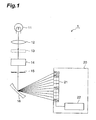
- Fig. 1 is a schematic diagram showing the construction of a spectroscopic device 1 according to an embodiment
- Fig. 2 is a diagram showing the construction of an image sensor 20A according to a first embodiment
- Fig. 3 is a timing chart showing the operation of the image sensor 20A according to the first embodiment
- Fig. 4 is a diagram showing the construction of an image sensor 20B according to a second embodiment.
- Fig. 5 is a timing chart showing the operation of the image sensor 20B according to the second embodiment.
- Fig. 1 is a diagram showing the construction of the spectroscopic device 1 according to the embodiment.
- the spectroscopic device 1 shown in Fig. 1 is provided with a light source 11, a lens 12, a shutter 13, a sample cell 14, a slit 15, a diffraction grating 16 and an image sensor 20.
- the light source 11 outputs light in some wavelength band, for example. It contains a deuterium lamp and a tungsten lamp, for example, and turns on these two lamps at the same time to output light in a broadband.
- the lens 12 condenses light output from the light source 11.
- the shutter 13 is provided at the rear stage of the condensing lens 12, and sets whether light is made incident to the sample cell 14.
- the sample cell 14 is a cell in which a sample as a measurement target is inserted. Light transmitted through the shutter 13 is made incident to the sample, and light transmitted through the sample is emitted.
- the diffraction grating 16 is a concave reflection type diffraction grating, and it acts as a spectroscope for inputting light emitted from the sample cell 14 and is then passed through the slit 15 and spectroscopically separates the light thus input.
- the image sensor 20 contains a photodiode array portion 21 and a signal processor 22.
- the photodiode array portion 21 includes N photodiodes PD 1 to PD N arranged, and receives light of each wavelength ⁇ n spectroscopically separated by the diffraction grating 16 by each photodiode PD n .
- the charge accumulation time in each photodiode PD n is variable.
- the signal processor 22 inputs charges output from each photodiode PD n contained in the photodiode array portion 21 and outputs the voltage value corresponding to the charge amount and the charge accumulation time.
- N represents an integer of 2 or more
- n represents any integer from not less than 1 to not more than N.
- the spectroscopic device 1 In this spectroscopic device 1, light output from the light source 11 is condensed by the lens 12, passed through the shutter 13 and then incident to the sample in the sample cell 14. Light out of the incident light, which is transmitted through the sample in the sample cell 14, is passed through the slit 15 and then spectroscopically separated by the diffraction grating 16. Light of each wavelength ⁇ n , thus spectroscopically separated is received by the photodiode PD n contained in the photodiode array portion 21. The voltage value corresponding to the amount of charges output from each photodiode PD n and the charge accumulation time is output from the signal processor 22.
- the spectrum of the light passed through the sample in the sample cell 14 is measured by the image sensor 20. Furthermore, the spectrum of light when no sample is inserted in the sample cell 14 is also measured by the image sensor 20. A transmission spectrum of the sample in the sample cell 14 is determined from the two spectra. It is preferable to carry out dark current correction on the basis of a result measured by the image sensor 20 in a state that the light source 11 is turned off and the shutter 13 is closed. Furthermore, it is also preferable to carry out background correction on the basis of a result measured by the image sensor 20 in a state that the light source 11 is turned off and the shutter 13 is opened.
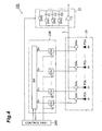
- FIG. 2 is a diagram showing the construction of an image sensor 20A according to the first embodiment.
- the image sensor 20A shown in Fig. 2 is suitably used as an image sensor 20 contained in the spectroscopic device 1 shown in Fig. 1 , and contains a switching instruction part 23A and a control part 24A in addition to the photodiode array portion 21 and the signal processor 22.
- the photodiode array portion 21 contains the N photodiode PD 1 to PD N and the N switches SW 1 to SW N .
- the anode terminal thereof is grounded and the cathode terminal thereof is connected to one end of the switch SW n , and it generates charges whose amount corresponds to the amount of light received.
- Each photodiode PD n accumulates the charges into the junction capacitance portion thereof when the switch SW n is opened, and outputs the charges to a common output line L when the switch SW n is closed.
- Each switch SW n is provided between the corresponding photodiode PD n and the common output line L.
- the signal processor 22 contains an amplifier A, capacitors C1 to C3 and switches SW0 to SW3.
- the input terminal of the amplifier A is connected to the common output line L.
- the capacitor C1 and the switch SW1 are connected to each other in series, and provided between the input and output terminals of the amplifier A.
- the capacitor C2 and the switch SW2 are connected to each other in series and provided between the input and output terminals of the amplifier A.
- the capacitor C3 and the switch SW3 are connected to each other in series, and provided between the input and output terminals of the amplifier A.
- the switch SW0 is provided between the input and output terminals of the amplifier A.
- the capacitors C1 to C3 and the switches SW1 to SW3 constitute the variable capacitance portion whose capacitance value is variable.
- the capacitance value of the variable capacitance portion is changed in accordance with the switching state of each of the switches SW1 to SW3.
- each of the capacitors C1 to C3 is discharged.
- the switch SW0 is opened, input charges are accumulated in the variable capacitance portion.
- the signal processor 22 can accumulate charges input from each photodiode PD n through the switch SW n and the common output line L into the variable capacitance portion, and output the voltage value corresponding to the ratio between the charge amount accumulated in the variable capacitance portion and the capacitance value of the variable capacitance portion.
- the switching instruction part 23A instructs the switching operation of each of the N switches SW 1 to SW N contained in the photodiode array portion 21.
- the switching instruction part 23A instructs the switching operation of each switch SW n so that the N switches SW 1 to SW N are set to the close state in different periods, and also the interval at which the respective switches SW n are set to the close state is equal to an integral multiple of a base period T.
- the switching instruction part 23A contains a shift register SR and N gate circuits G 1 to G N .
- the shift register SR successively outputs the switching instruction signals S 1 to S N for instructing the switching operation of the N switches SW 1 to SW N as a value instructing the close state on the basis of a start signal and a clock signal output from the control part 24A.
- Each gate circuit G n is provided in correspondence with the switch SW n . It inputs the switching instruction signal S n output from the shift register SR, and also inputs a control signal T n output from the control part 24A.
- each gate circuit G n When the control signal T n is equal to a first value, each gate circuit G n directly outputs the switching instruction signal S n to the switch SW n , and when the control signal T n is equal to a second value, each gate circuit G n outputs the switching instruction signal having a value indicating the open state to the switch SW n .
- a proper logic circuit (AND circuit, OR circuit, NAND circuit, NOR circuit or the like) is selected for each gate circuit G n in accordance with the polarity of the signal instructing the switching operation of the switch SW n , the polarity of the switching instruction signal S n output from the shift register SR and the polarity of the control signal T n output from the control part 24A.
- the switch SW n is closed when the signal instructing the switching operation of the switch SW n is set to a high level
- the switching instruction signal S n instructs the close state of the switch SW n when the switching instruction signal S n output from the shift register SR is set to a high level
- the gate circuit G n directly outputs the switching instruction signal S n to the switch SW n when the control signal T n output from the control part 24A is set to a high level.
- the gate circuit G n may be constructed by an AND circuit. This condition is assumed to be satisfied when the operation is described hereunder.
- the control part 24A outputs a signal for controlling the operation of each of the signal processor 22 and the switching instruction part 23A. Specifically, the control part 24A outputs a signal for controlling the switching operation of each of the switches SW0 to SW3 contained in the signal processor 22, outputs the start signal and the clock signal to the shift register SR contained in the switching instruction part 23A, and outputs the control signal T n to each gate circuit G n contained in the switching instruction part 23A.
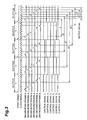
- Fig. 3 is a timing chart showing the operation of the image sensor 20A according to the first embodiment.
- the start signal and the clock signal supplied from the control part 24A to the shift register SR, the switching instruction signals S 1 to S 6 output from the shift register SR, the control signals T 1 to T 6 supplied from the control part 24A to the gate circuits G 1 to G 6 and the amount of charges passed through the common output line L and input to the signal processor 22 are shown from the upper side in Fig. 3 .
- the value of N is set to 6. Furthermore, it is assumed that the switching instruction part 23A instructs the switching operation of each switch SW n so that the interval at which each switch SW n is set to the close state is equal to be one to four times as long as the base period T.
- Each of the start signal and the clock signal supplied from the control part 24A to the shift register SR is a periodic signal whose level is varied at a fixed period.
- the period of the start signal is represented by T, and the period of the clock signal is shorter than T.
- the period from some rising time of the start signal until the next rising time is referred to as "cycle.”
- the time of each cycle is equal to T.
- the shift register SR is initialized at the rising time of the start signal, and then the switching instruction signals S 1 to S 6 for instructing the switching operation of the respective switches SW 1 to SW 6 are successively output as a value instructing the close state at each rising time of the subsequent clock signal. That is, in each cycle, the switching instruction signals S 1 to S 6 output from the shift register SR are successively set to a high level.
- the control signals T 1 to T 6 supplied from the control part 24A to the gate circuits G 1 to G 6 are as follows. Each of the control signals T 1 and T 6 is set to a high level in a first cycle, to a low level in second and third cycles, and to a high level in fourth and fifth cycles. Each of the control signals T 2 and T 5 is set to a high level in the first cycle, to a low level in the second cycle, to a high level in the third cycle, to a low level in the fourth cycle, and to a high level in the fifth cycle.
- the control signal T 3 is set to a high level in the first and second cycles, to a low level in the third and fourth cycles, and to a high level in the fifth cycle. Furthermore, the control signal T 4 is set to a high level in the first cycle, to a low level in the second to fourth cycles and to a high level in the fifth cycle.
- the switching instruction signal output from each gate circuit G n to the switch SW n is still the switching instruction signal S n output from the shift register SR during the cycle in which the control signal T n is set to a high level, however, it has a value instructing the open state during the cycle in which the control signal T n is set to a low level. That is, the switching instruction signal supplied from each gate circuit G n to the switch SW n has a value instructing the close state when both the switching instruction signal S n output from the shift register SR and the control signal T n are set to a high level, and it has a value instructing the open state when any one of the switching instruction signal S n and the control signal T n is set to a low level.
- the switching instruction signal output from the gate circuit G 1 to the switch SW 1 is still the switching instruction signal S 1 output from the shift register SR in the first, fourth and fifth cycles, however, it has a value instructing the open state in the other cycles.
- the switching instruction signal output from the gate circuit G 2 to the switch SW 2 is still the switching instruction signal S 2 output from the shift register SR in the first, third and fifth cycles, however, it has a value instructing the open state in the other cycles.
- the switching instruction signal output from the gate circuit G 3 to the switch SW 3 is still the switching instruction signal S 3 output from the shift register SR in the first, second and fifth cycles, however, it has a value instructing the open state in the other cycles.
- the switching instruction signal output from the gate circuit G 4 to the switch SW 4 is still the switching instruction signal S 4 output from the shift register SR in the first and fifth cycles, however, it has a value instructing the open state in the other cycles.
- the switching instruction signal output from the gate circuit G 5 to the switch SW 5 is still the switching instruction signal S 5 output from the shift register SR in the first, third and fifth cycles, however, it has a value instructing the open state in the other cycles.
- the switching instruction signal output from the gate circuit G 6 to the switch SW 6 is still the switching instruction signal S 6 output from the shift register SR in the first, fourth and fifth cycles, however, it has a value instructing the open state in the other cycles.
- Each switch SW n contained in the photodiode array portion 21 is closed for some period when the switching instruction signal arriving from the gate circuit G n is set to a high level, and opened in another period. In each of the first and fifth cycles, the switches SW 1 to SW 6 are successively closed.
- the switch SW 1 is closed when the switching instruction signal S 1 is set to a high level during the fifth cycle, whereby the charges accumulated in the junction capacitance portion of the photodiode PD 1 are output to the signal processor 22 via the common output line L during the period T subsequent to the time when the switching instruction signal S 1 is set to a high level during the preceding fourth cycle.
- the switch SW 2 is closed when the switching instruction signal S 2 is set to a high level during the fifth cycle, whereby the charges accumulated in the junction capacitance portion of the photodiode PD 2 are output to the signal processor 22 via the common output line L during the time 2T subsequent to the time when the switching instruction signal S 2 is set to a high level during the preceding third cycle.
- the switch SW 3 is closed when the switching instruction signal S 3 is set to a high level during the fifth cycle, whereby the charges accumulated in the junction capacitance portion of the photodiode PD 3 are output to the signal processor 22 via the common output line L during the time 3T subsequent to the time when the switching instruction signal S 3 is set to a high level during the preceding second cycle.
- the switch SW 4 is closed when the switching instruction signal S 4 is set to a high level during the fifth cycle, whereby the charges accumulated in the junction capacitance portion of the photodiode PD 4 are output to the signal processor 22 via the common output line L during the time 4T subsequent to the time when the switching instruction signal S 4 is set to a high level during the preceding first cycle.
- the switch SW 5 is closed when the switching instruction signal S 5 is set to a high level during the fifth cycle, whereby the charges accumulated in the junction capacitance portion of the photodiode PD 5 are output to the signal processor 22 via the common output line L during the time 2T subsequent to the time when the switching instruction signal S 5 is set to a high level during the preceding third cycle.
- the switch SW 6 is closed when the switching instruction signal S 6 is set to a high level during the fifth cycle, whereby the charges accumulated in the junction capacitance portion of the photodiode PD 6 are output to the signal processor 22 via the common output line L during the period T subsequent to the time when the switching instruction signal S 6 is set to a high level during the preceding fourth cycle.
- the charges passed through the common output line L and then input to the processor 22 in the fifth cycle correspond to the charges accumulated in the junction capacitance portion during the period T with respect to the photodiode PD1, the charges accumulated in the junction capacitance portion during the time 2T with respect to the photodiode PD 2 , the charges accumulated in the junction capacitance portion during the time 3T with respect to the photodiode PD 3 , the charges accumulated in the junction capacitance portion during the time 4T with respect to the photodiode PD 4 , the charges accumulated in the junction capacitance portion during the time 2T with respect to the photodiode PD 5 , and the charges accumulated in the junction capacitance portion during the period T with respect to the photodiode PD 6 .
- the interval at which each switch SW n is set to the close state is equal to an integral multiple of the base period T, whereby the charge accumulation time in each photodiode PD n is also equal to
- the charges which are passed from each photodiode PD n through the switch SW n and the common output line L and then input to the signal processor 22 are accumulated in the variable capacitance portion of the signal processor 22, and the voltage value corresponding to the ratio between the amount of charges accumulated in the variable capacitance portion and the capacitance value of the variable capacitance portion is output from the signal processor 22.
- the capacitance value of the variable capacitance portion is set in proportion to the charge accumulation time in each photodiode PD n for generating charges to be accumulated.
- the capacitance value of the variable capacitance portion is set to C.
- the capacitance value of the variable capacitance portion is set to 2C.
- the capacitance value of the variable capacitance portion is set to 3C.
- the capacitance value of the variable capacitance portion is set to 4C.
- the capacitance value of the variable capacitance portion is set to 2C.
- the capacitance value of the variable capacitance portion is set to C.
- the interval at which each switch SW n is set to the close state is set to an integral multiple of the base period T, whereby the charge accumulation time in each photodiode PD n can be set to an integral multiple of the base period T. Accordingly, with respect to each photodiode PD n , the charge accumulation time can be changed to the extent that the accumulated charge amount in the junction capacitance portion is not saturated. Accordingly, the spectroscopic device 1 provided with the image sensor 20A as described above can perform high-sensitivity spectroscopic measurements in each wavelength.
- each photodiode PD n by changing the capacitance value of the variable capacitance portion of the signal processor 22 in accordance with the charge accumulation time, the effect caused by the difference in charge accumulation time between the respective photodiodes PD n is excluded from the voltage value output from the signal processor 22.
- the setting of the charge accumulating time in each photodiode PD n is carried out as follows. First, in the state that the charge accumulation time in each of the photodiodes PD 1 to PD N is set as the base period T and the capacitance value of the variable capacitance portion of the signal processor 22 is set to C, when light having excessive intensity is made incident to each photodiode PD n and the accumulated charge amount in the junction capacitance portion of the photodiode PD n is saturated, the voltage value V sat output from the signal processor 22 is determined. Furthermore, in this state, light to be measured is made incident to each photodiode PD n , and the voltage value V n output from the signal processor 22 is determined.
- Fig. 4 is a diagram showing the construction of an image sensor 20B according to the second embodiment.
- the image sensor 20B shown in Fig. 4 is suitably used as the image sensor 20 contained in the spectroscopic device 1 shown in Fig. 1 , and it further contains a switching instruction part 23B and a control part 24B in addition to the photodiode array portion 21 and the signal processor 22.
- the image sensor 20B according to the second embodiment shown in Fig. 4 has the same construction with respect to the photodiode array portion 21 and the signal processor 22, however, it is different in that it contains a switching instruction part 23B in place of the switching instruction part 23A, and also in that it contains a control part 24B in place of the control part 24A.
- the switching instruction part 23B instructs the switching operation of each of the N switches SW 1 to SW N contained in the photodiode array portion 21. Particularly, the switching instruction part 23B instructs the switching operation of each switch SW n so that the N switches SW 1 to SW N are set to the close state in different periods, and also the interval at which each switch SW n is set to the close state is equal to an integral multiple of the base period T.
- the switching instruction part 23B contains the shift register SR and the N gate circuits G 1 to G N .
- the shift register SR On the basis of the start signal and the clock signal output from the control part 24B, the shift register SR successively outputs the switching instruction signals S 1 to S N for instructing the switching operation of the respective N switches SW 1 to SW N as a value instructing the close state.
- Each gate circuit G n is provided in correspondence with the switch SW n . It inputs the switching instruction signal S n output from the shift register SR and also inputs a common control signal T 0 output from the control part 24B.
- each gate circuit G n When the control signal T 0 is equal to a first value, each gate circuit G n directly outputs the switching instruction signal S n to the switch SW n , and when the control signal T 0 is equal to a second value, each gate circuit G n outputs the switching instruction signal having a value instructing the open state to the switch SW n .
- a proper logic circuit (AND circuit, OR circuit, NAND circuit, NOR circuit or the like) is selected in accordance with the polarity of a signal instructing the switching operation of the switch SW n , the polarity of the switching instruction signal S n output from the shift register SR and the polarity of the control signal T 0 output from the control part 24B.
- the switch SW n when the signal instructing the switching operation of the switch SW n is set to a high level, the switch SW n is closed, when the switching instruction signal S n output from the shift register SR is set to a high level, the switching instruction signal S n instructs the close state of the switch SW n and when the control signal T 0 output from the control part 24B is set to a high level, the gate circuit G n directly outputs the switching instruction signal S n to the switch SW n .
- the gate circuit G n may be constructed by an AND circuit. This condition is satisfied when the operation is described below.
- the control part 24B outputs signals for controlling the operation of the signal processor 22 and the switching instruction part 23B. Specifically, the control part 24B outputs a signal for controlling the switching operation of each of the switches SW0 to SW3 contained in the signal processor 22, outputs the start signal and the clock signal to the shift register SR contained in the switching instruction part 23B and outputs the common control signal T 0 to each gate circuit G n contained in the switching instruction part 23B.
- Fig 5 is a timing chart showing the operation of the image sensor 20B according to the second embodiment.
- the start signal and the clock signal supplied from the control part 24B to the shift register SR, the switching instruction signals S 1 to S 6 output from the shift register SR, the common control signal T 0 supplied from the control part 24B to the gate circuits G 1 to G 6 and the amount of charges input to the signal processor 22 through the common output line L are shown from the upper side in Fig. 5 .
- the switching instruction part 23B instructs the switching operation of each switch SW n so that the interval at which each switch SW n is set to the close state is set to one to four times of the base period T.
- the start signal and the clock signal supplied from the control part 24B to the shift register SR and the switching instruction signals S 1 to S 6 output from the shift register SR are the same as the first embodiment.
- the common control signal T 0 supplied from the control part 24B to the gate circuits G 1 to G 6 is as follows. In the first and fifth cycles, the control signal T 0 is set to a high level during the period when any one of the switching instruction signals S 1 to S 6 output from the shift register SR is set to a high level, and in the other period, the control signal T 0 is set to a low level. In the second cycle, during the period when the switching instruction signal S 3 output from the shift register SR is set to a high level, the control signal T 0 is set to a high level, and in the other period, the control signal T 0 is set to a low level.
- the control signal T 0 is set to a high level, and in the other period, the control signal T 0 is set to a low level.
- the control signal T 0 is set to a high level, and in the other period, the control signal T 0 is set to a low level.
- the switching instruction signal output from each gate circuit G n to the switch SW n is still the switching instruction signal S n output from the shift register SR for the period when the control signal T 0 is set to a high level, however, it has a value instructing the open state during the period when the control signal T 0 is set to a low level. That is, the switching instruction signal from each gate circuit G n to the switch SW n has a value instructing the close state when both the switching instruction signal S n output from the shift register SR and the control signal T 0 are set to a high level, however, it has a value instructing the open state when any one of the switching instruction signal S n and the control signal T 0 is set to a low level.
- the switching instruction signal output from the gate circuit G 1 to the switch SW 1 is still the switching instruction signal S 1 output from the shift register SR in the first, fourth and fifth cycles, however, it has a value instructing the open state in the other cycles.
- the switching instruction signal output from the gate circuit G 2 to the switch SW 2 is still the switching instruction signal S 2 output from the shift register SR in the first, third and fifth cycles, however, it has a value instructing the open state in the other cycles.
- the switching instruction signal output from the gate circuit G 3 to the switch SW 3 is still the switching instruction signal S 3 output from the shift register SR in the first, second and fifth cycles, however, it has a value instructing the open state in the other cycles.
- the switching instruction signal output from the gate circuit G 4 to the switch SW 4 is still the switching instruction signal S 4 output from the shift register SR in the first and fifth cycles, however, it has a value instructing the open state in the other cycles.
- the switching instruction signal output from the gate circuit G 5 to the switch SW 5 is still the switching instruction signal S 5 output from the shift register SR in the first, third and fifth cycles, however, it has a value instructing the open state in the other cycles.
- the switching instruction signal output from the gate circuit G 6 to the switch SW 6 is still the switching instruction signal S 6 output from the shift register SR in the first, fourth and fifth cycles, however, it has a value instructing the open state in the other cycles.
- Each switch SW n contained in the photodiode array portion 21 is closed during the period when the switching instruction signal arriving from the gate circuit G n is set to a high level, and it is opened in the other period.
- the switching operation of each switch SW n and the operation of the signal processor 22 are the same as the operation of the first embodiment.
- the image sensor 20B by setting the interval of the close state of each switch SW n to an integral multiple of the base period T, the charge accumulation time in each photodiode PD n can be set to an integral multiple of the base period T, whereby the charge accumulation time can be changed to the extent that the accumulated charge amount in the junction capacitance portion with respect to each photodiode PD n is not saturated. Accordingly, the spectroscopic device 1 having the image sensor 20B as described above can perform high-sensitivity spectroscopic measurement in each wavelength.
- the effect caused by the difference in charge accumulation time among the respective photodiodes PD n is excluded from the voltage value output from the signal processor 22.
- the common control signal T 0 is supplied from the control part 24B to the N gate circuits G 1 to G N , and thus it is sufficient to provide only one wire for the control signal T 0 . Accordingly, the image sensor 20B according to the second embodiment can be miniaturized, and thus manufactured at a low price.
Description
- The present invention relates to an image sensor containing plural photodiodes.
- An image sensor containing plural photodiodes is used for a spectroscopic device, for example. In the spectroscopic device, light in some wavelength band which is output from a light source is made incident to a sample, light which is a part of the incident light and transmitted through the sample is spectroscopically separated by a spectroscope, and then the spectroscopically separated light beams having respective wavelengths are detected by the image sensor. In such a spectroscopic device, it is common that the intensity spectrum I(λ) of light output from the light source and the detecting sensitivity spectrum D(λ) of each photodiode contained in the image sensor are not flat in wavelength bands used for spectroscopic measurements.
- Furthermore, the photodiode generates charges whose amount corresponds to the amount of light received, and accumulates the thus generated charges into a junction capacitance portion. When the junction capacitance portion is electrically connected to another circuit, the charges which have been accumulated in the junction capacitance portion until then are transmitted to the circuit concerned. However, the amount of charges to be accumulated in the junction capacitance portion of the photodiode is limited. When the amount of light received is small, the accumulated charge amount is proportional to the amount of light received, however, when the amount of light received is large, the accumulated charge amount is saturated.
- As described above, it is required to set the charge accumulation time in the spectroscopic device so that the accumulated charge amount in the junction capacitance portion of the photodiode is not saturated at a wavelength λ at which the product (I(λ)•D(λ)) with the intensity spectrum I(λ) of light output from the light source and the detecting sensitivity spectrum D(λ) of the photodiode has a peak. An image sensor contained in a spectroscopic device disclosed in Japanese Patent No.
3,572,681 - In the spectroscopic device containing the image sensor as disclosed in the
above Patent Document 1, it is possible to carry out a high-sensitivity spectroscopic measurement in a wavelength range where the product (I(λ)•D(λ)) is large. However, in a wavelength range where the product (I(λ)•D(λ)) is small, noise components cannot be disregarded with respect to signal components and thus the sensitivity is low.US Patent 4,674,880 EP 355174 EP 399057 - The present invention has been implemented to solve the above problem point, and has an object to provide a spectroscopic device that can perform high-sensitivity spectroscopic measurements in each wavelength, and an image sensor suitably used for the spectroscopic device as described above.
- The present invention is an image sensor according to
claim 1 or claim 2. - The switching instruction part contains (a) a shift register for successively outputting each of switching instruction signals S1 to SN for instructing the switching operation of the N switches SW1 to SWN as a value instructing the close state, and (b) N gate circuits G1 to GN that are provided in one-to-one correspondence to the N switches SW1 to SWN. In this case, it is preferable that each gate circuit Gn inputs the switching instruction signal Sn output from the shift register and also inputs a control signal Tn, whereby when the control signal Tn is equal to a first value, each gate circuit Gn directly outputs the switching instruction signal Sn to the switch SWn, and when the control signal Tn is equal to a second value, each gate circuit Gn outputs the switching instruction signal having a value instructing an open state to the switch SWn. It is also preferable that each gate circuit Gn inputs the switching instruction signal Sn output from the shift register and also inputs a common control signal To, whereby when the control signal To is equal to a first value, each gate circuit Gn directly outputs the switching instruction signal Sn to the switch SWn, and when the control signal To is equal to a second value, each gate circuit Gn outputs the switching instruction signal having a value instructing an open state to the switch SWn. Each gate circuit Gn is constructed by a logic circuit such as an AND circuit or the like, and the first value and the second value are set so that one of the values is set to a high level while the other is set to a low level.
- When the switching instruction part is constructed as described above, each switching instruction signal Sn for instructing the switching operation of the switch SWn is output from the shift register and input to the gate circuit Gn. The switching instruction signal supplied from each gate circuit Gn to the switch SWn remains as the switching instruction signal Sn when the control signal Tn or the common control signal T0 is equal to the first value, and the switching instruction signal concerned is set to the value instructing the open state when the control signal Tn or the common control signal T0 is equal to the second value. That is, the charge accumulation time of the photodiode PDn is set to an integral multiple of the base period on the basis of the control signal Tn or the common control signal T0.
- The image sensor according to the present invention is further provided with a signal processor for accumulating charges input from each photodiode PDn through the switch SWn and the common output line into a variable capacitance portion whose capacitance value is variable, and outputting the voltage value corresponding to the ratio between the amount of charges accumulated in the variable capacitance portion and the capacitance value of the variable capacitance portion. In this case, the charges output from each photodiode PDn through the switch SWn to the common output line are input to the signal processor and accumulated in the variable capacitance portion contained in the signal processor, and the voltage value corresponding to the ratio between the amount of charges accumulated in the variable capacitance portion and the capacitance value of the variable capacitance portion is output from the signal processor.
- A spectroscopic device according to the present invention is characterized by including: a light source for outputting light; a spectroscope for spectroscopically separating light output from the light source and transmitted through a sample; and the above-described image sensor for receiving light of each wavelength which is spectroscopically separated by the spectroscope. In the spectroscopic device, light which is a part of light output from the light source and transmitted through the sample is spectroscopically separated by the spectroscope and then received by the image sensor.
- According to the present invention, a high-sensitivity spectroscopic measurement can be performed at each wavelength.
-
Fig. 1 is a schematic diagram showing the construction of aspectroscopic device 1 according to an embodiment; -
Fig. 2 is a diagram showing the construction of animage sensor 20A according to a first embodiment; -
Fig. 3 is a timing chart showing the operation of theimage sensor 20A according to the first embodiment; -
Fig. 4 is a diagram showing the construction of animage sensor 20B according to a second embodiment; and -
Fig. 5 is a timing chart showing the operation of theimage sensor 20B according to the second embodiment. - Preferred embodiments for implementing the present invention will be described in detail with reference to the accompanying drawings. In the description of the drawings, the same elements are represented by the same reference numerals, and overlapping description thereof is omitted.
- (Embodiment of Spectroscopic Device)
- First, an embodiment of the spectroscopic device according to the present invention will be described.
Fig. 1 is a diagram showing the construction of thespectroscopic device 1 according to the embodiment. Thespectroscopic device 1 shown inFig. 1 is provided with alight source 11, alens 12, ashutter 13, asample cell 14, aslit 15, a diffraction grating 16 and animage sensor 20. - The
light source 11 outputs light in some wavelength band, for example. It contains a deuterium lamp and a tungsten lamp, for example, and turns on these two lamps at the same time to output light in a broadband. Thelens 12 condenses light output from thelight source 11. Theshutter 13 is provided at the rear stage of thecondensing lens 12, and sets whether light is made incident to thesample cell 14. Thesample cell 14 is a cell in which a sample as a measurement target is inserted. Light transmitted through theshutter 13 is made incident to the sample, and light transmitted through the sample is emitted. The diffraction grating 16 is a concave reflection type diffraction grating, and it acts as a spectroscope for inputting light emitted from thesample cell 14 and is then passed through theslit 15 and spectroscopically separates the light thus input. - The
image sensor 20 contains aphotodiode array portion 21 and asignal processor 22. Thephotodiode array portion 21 includes N photodiodes PD1 to PDN arranged, and receives light of each wavelength λn spectroscopically separated by the diffraction grating 16 by each photodiode PDn. The charge accumulation time in each photodiode PDn is variable. Thesignal processor 22 inputs charges output from each photodiode PDn contained in thephotodiode array portion 21 and outputs the voltage value corresponding to the charge amount and the charge accumulation time. Here, N represents an integer of 2 or more, and n represents any integer from not less than 1 to not more than N. - In this
spectroscopic device 1, light output from thelight source 11 is condensed by thelens 12, passed through theshutter 13 and then incident to the sample in thesample cell 14. Light out of the incident light, which is transmitted through the sample in thesample cell 14, is passed through theslit 15 and then spectroscopically separated by the diffraction grating 16. Light of each wavelength λn, thus spectroscopically separated is received by the photodiode PDn contained in thephotodiode array portion 21. The voltage value corresponding to the amount of charges output from each photodiode PDn and the charge accumulation time is output from thesignal processor 22. - As described above, the spectrum of the light passed through the sample in the
sample cell 14 is measured by theimage sensor 20. Furthermore, the spectrum of light when no sample is inserted in thesample cell 14 is also measured by theimage sensor 20. A transmission spectrum of the sample in thesample cell 14 is determined from the two spectra. It is preferable to carry out dark current correction on the basis of a result measured by theimage sensor 20 in a state that thelight source 11 is turned off and theshutter 13 is closed. Furthermore, it is also preferable to carry out background correction on the basis of a result measured by theimage sensor 20 in a state that thelight source 11 is turned off and theshutter 13 is opened. - (First Embodiment of Image Sensor)
- Next, a first embodiment of the image sensor according to the present invention will be described.
Fig. 2 is a diagram showing the construction of animage sensor 20A according to the first embodiment. Theimage sensor 20A shown inFig. 2 is suitably used as animage sensor 20 contained in thespectroscopic device 1 shown inFig. 1 , and contains a switchinginstruction part 23A and acontrol part 24A in addition to thephotodiode array portion 21 and thesignal processor 22. - The
photodiode array portion 21 contains the N photodiode PD1 to PDN and the N switches SW1 to SWN. With respect to each photodiode PDn, the anode terminal thereof is grounded and the cathode terminal thereof is connected to one end of the switch SWn, and it generates charges whose amount corresponds to the amount of light received. Each photodiode PDn accumulates the charges into the junction capacitance portion thereof when the switch SWn is opened, and outputs the charges to a common output line L when the switch SWn is closed. Each switch SWn is provided between the corresponding photodiode PDn and the common output line L. - The
signal processor 22 contains an amplifier A, capacitors C1 to C3 and switches SW0 to SW3. The input terminal of the amplifier A is connected to the common output line L. The capacitor C1 and the switch SW1 are connected to each other in series, and provided between the input and output terminals of the amplifier A. The capacitor C2 and the switch SW2 are connected to each other in series and provided between the input and output terminals of the amplifier A. The capacitor C3 and the switch SW3 are connected to each other in series, and provided between the input and output terminals of the amplifier A. The switch SW0 is provided between the input and output terminals of the amplifier A. - The capacitors C1 to C3 and the switches SW1 to SW3 constitute the variable capacitance portion whose capacitance value is variable. The capacitance value of the variable capacitance portion is changed in accordance with the switching state of each of the switches SW1 to SW3. When all the switches SW0 to SW3 are closed, each of the capacitors C1 to C3 is discharged. Furthermore, when the switch SW0 is opened, input charges are accumulated in the variable capacitance portion. The
signal processor 22 can accumulate charges input from each photodiode PDn through the switch SWn and the common output line L into the variable capacitance portion, and output the voltage value corresponding to the ratio between the charge amount accumulated in the variable capacitance portion and the capacitance value of the variable capacitance portion. - The switching
instruction part 23A instructs the switching operation of each of the N switches SW1 to SWN contained in thephotodiode array portion 21. In particular, the switchinginstruction part 23A instructs the switching operation of each switch SWn so that the N switches SW1 to SWN are set to the close state in different periods, and also the interval at which the respective switches SWn are set to the close state is equal to an integral multiple of a base period T. - Specifically, the switching
instruction part 23A contains a shift register SR and N gate circuits G1 to GN. The shift register SR successively outputs the switching instruction signals S1 to SN for instructing the switching operation of the N switches SW1 to SWN as a value instructing the close state on the basis of a start signal and a clock signal output from thecontrol part 24A. Each gate circuit Gn is provided in correspondence with the switch SWn. It inputs the switching instruction signal Sn output from the shift register SR, and also inputs a control signal Tn output from thecontrol part 24A. When the control signal Tn is equal to a first value, each gate circuit Gn directly outputs the switching instruction signal Sn to the switch SWn, and when the control signal Tn is equal to a second value, each gate circuit Gn outputs the switching instruction signal having a value indicating the open state to the switch SWn. - A proper logic circuit (AND circuit, OR circuit, NAND circuit, NOR circuit or the like) is selected for each gate circuit Gn in accordance with the polarity of the signal instructing the switching operation of the switch SWn, the polarity of the switching instruction signal Sn output from the shift register SR and the polarity of the control signal Tn output from the
control part 24A. For example, it is assumed that the switch SWn is closed when the signal instructing the switching operation of the switch SWn is set to a high level, the switching instruction signal Sn instructs the close state of the switch SWn when the switching instruction signal Sn output from the shift register SR is set to a high level, and the gate circuit Gn directly outputs the switching instruction signal Sn to the switch SWn when the control signal Tn output from thecontrol part 24A is set to a high level. In this case, the gate circuit Gn may be constructed by an AND circuit. This condition is assumed to be satisfied when the operation is described hereunder. - The
control part 24A outputs a signal for controlling the operation of each of thesignal processor 22 and the switchinginstruction part 23A. Specifically, thecontrol part 24A outputs a signal for controlling the switching operation of each of the switches SW0 to SW3 contained in thesignal processor 22, outputs the start signal and the clock signal to the shift register SR contained in the switchinginstruction part 23A, and outputs the control signal Tn to each gate circuit Gn contained in the switchinginstruction part 23A. - Next, an example of the operation of the
image sensor 20A according to the first embodiment will be described.Fig. 3 is a timing chart showing the operation of theimage sensor 20A according to the first embodiment. The start signal and the clock signal supplied from thecontrol part 24A to the shift register SR, the switching instruction signals S1 to S6 output from the shift register SR, the control signals T1 to T6 supplied from thecontrol part 24A to the gate circuits G1 to G6 and the amount of charges passed through the common output line L and input to thesignal processor 22 are shown from the upper side inFig. 3 . - In this case, the value of N is set to 6. Furthermore, it is assumed that the switching
instruction part 23A instructs the switching operation of each switch SWn so that the interval at which each switch SWn is set to the close state is equal to be one to four times as long as the base period T. The capacitance values of the capacitors C1 to C3 contained in thesignal processor 22 may be set to C, 2C and 4C, and the capacitance value of the variable capacitance portion may be set to any one of C, 2C, 3C (=C+2C) and 4C. The following operation is carried out under the control of thecontrol part 24A. - Each of the start signal and the clock signal supplied from the
control part 24A to the shift register SR is a periodic signal whose level is varied at a fixed period. The period of the start signal is represented by T, and the period of the clock signal is shorter than T. In the following description, the period from some rising time of the start signal until the next rising time is referred to as "cycle." The time of each cycle is equal to T. Furthermore, the clock signal contains at least N (in this case, N=6) pulses for the period from some falling time of the start signal until the next rising time. - The shift register SR is initialized at the rising time of the start signal, and then the switching instruction signals S1 to S6 for instructing the switching operation of the respective switches SW1 to SW6 are successively output as a value instructing the close state at each rising time of the subsequent clock signal. That is, in each cycle, the switching instruction signals S1 to S6 output from the shift register SR are successively set to a high level.
- The control signals T1 to T6 supplied from the
control part 24A to the gate circuits G1 to G6 are as follows. Each of the control signals T1 and T6 is set to a high level in a first cycle, to a low level in second and third cycles, and to a high level in fourth and fifth cycles. Each of the control signals T2 and T5 is set to a high level in the first cycle, to a low level in the second cycle, to a high level in the third cycle, to a low level in the fourth cycle, and to a high level in the fifth cycle. The control signal T3 is set to a high level in the first and second cycles, to a low level in the third and fourth cycles, and to a high level in the fifth cycle. Furthermore, the control signal T4 is set to a high level in the first cycle, to a low level in the second to fourth cycles and to a high level in the fifth cycle. - The switching instruction signal output from each gate circuit Gn to the switch SWn is still the switching instruction signal Sn output from the shift register SR during the cycle in which the control signal Tn is set to a high level, however, it has a value instructing the open state during the cycle in which the control signal Tn is set to a low level. That is, the switching instruction signal supplied from each gate circuit Gn to the switch SWn has a value instructing the close state when both the switching instruction signal Sn output from the shift register SR and the control signal Tn are set to a high level, and it has a value instructing the open state when any one of the switching instruction signal Sn and the control signal Tn is set to a low level.
- Accordingly, the switching instruction signal output from the gate circuit G1 to the switch SW1 is still the switching instruction signal S1 output from the shift register SR in the first, fourth and fifth cycles, however, it has a value instructing the open state in the other cycles. The switching instruction signal output from the gate circuit G2 to the switch SW2 is still the switching instruction signal S2 output from the shift register SR in the first, third and fifth cycles, however, it has a value instructing the open state in the other cycles.
- The switching instruction signal output from the gate circuit G3 to the switch SW3 is still the switching instruction signal S3 output from the shift register SR in the first, second and fifth cycles, however, it has a value instructing the open state in the other cycles. The switching instruction signal output from the gate circuit G4 to the switch SW4 is still the switching instruction signal S4 output from the shift register SR in the first and fifth cycles, however, it has a value instructing the open state in the other cycles.
- The switching instruction signal output from the gate circuit G5 to the switch SW5 is still the switching instruction signal S5 output from the shift register SR in the first, third and fifth cycles, however, it has a value instructing the open state in the other cycles. The switching instruction signal output from the gate circuit G6 to the switch SW6 is still the switching instruction signal S6 output from the shift register SR in the first, fourth and fifth cycles, however, it has a value instructing the open state in the other cycles.
- Each switch SWn contained in the
photodiode array portion 21 is closed for some period when the switching instruction signal arriving from the gate circuit Gn is set to a high level, and opened in another period. In each of the first and fifth cycles, the switches SW1 to SW6 are successively closed. - The switch SW1 is closed when the switching instruction signal S1 is set to a high level during the fifth cycle, whereby the charges accumulated in the junction capacitance portion of the photodiode PD1 are output to the
signal processor 22 via the common output line L during the period T subsequent to the time when the switching instruction signal S1 is set to a high level during the preceding fourth cycle. The switch SW2 is closed when the switching instruction signal S2 is set to a high level during the fifth cycle, whereby the charges accumulated in the junction capacitance portion of the photodiode PD2 are output to thesignal processor 22 via the common output line L during thetime 2T subsequent to the time when the switching instruction signal S2 is set to a high level during the preceding third cycle. - The switch SW3 is closed when the switching instruction signal S3 is set to a high level during the fifth cycle, whereby the charges accumulated in the junction capacitance portion of the photodiode PD3 are output to the
signal processor 22 via the common output line L during thetime 3T subsequent to the time when the switching instruction signal S3 is set to a high level during the preceding second cycle. The switch SW4 is closed when the switching instruction signal S4 is set to a high level during the fifth cycle, whereby the charges accumulated in the junction capacitance portion of the photodiode PD4 are output to thesignal processor 22 via the common output line L during thetime 4T subsequent to the time when the switching instruction signal S4 is set to a high level during the preceding first cycle. - The switch SW5 is closed when the switching instruction signal S5 is set to a high level during the fifth cycle, whereby the charges accumulated in the junction capacitance portion of the photodiode PD5 are output to the
signal processor 22 via the common output line L during thetime 2T subsequent to the time when the switching instruction signal S5 is set to a high level during the preceding third cycle. The switch SW6 is closed when the switching instruction signal S6 is set to a high level during the fifth cycle, whereby the charges accumulated in the junction capacitance portion of the photodiode PD6 are output to thesignal processor 22 via the common output line L during the period T subsequent to the time when the switching instruction signal S6 is set to a high level during the preceding fourth cycle. - As described above, the charges passed through the common output line L and then input to the
processor 22 in the fifth cycle correspond to the charges accumulated in the junction capacitance portion during the period T with respect to the photodiode PD1, the charges accumulated in the junction capacitance portion during thetime 2T with respect to the photodiode PD2, the charges accumulated in the junction capacitance portion during thetime 3T with respect to the photodiode PD3, the charges accumulated in the junction capacitance portion during thetime 4T with respect to the photodiode PD4, the charges accumulated in the junction capacitance portion during thetime 2T with respect to the photodiode PD5, and the charges accumulated in the junction capacitance portion during the period T with respect to the photodiode PD6. As described above, the interval at which each switch SWn is set to the close state is equal to an integral multiple of the base period T, whereby the charge accumulation time in each photodiode PDn is also equal to an integral multiple of the base period T. - In the fifth cycle, the charges which are passed from each photodiode PDn through the switch SWn and the common output line L and then input to the
signal processor 22 are accumulated in the variable capacitance portion of thesignal processor 22, and the voltage value corresponding to the ratio between the amount of charges accumulated in the variable capacitance portion and the capacitance value of the variable capacitance portion is output from thesignal processor 22. The capacitance value of the variable capacitance portion is set in proportion to the charge accumulation time in each photodiode PDn for generating charges to be accumulated. - That is, when the charges input from the photodiode PD1 are accumulated in the variable capacitance portion, the capacitance value of the variable capacitance portion is set to C. When the charges input from the photodiode PD2 are accumulated in the variable capacitance portion, the capacitance value of the variable capacitance portion is set to 2C. When the charges input from the photodiode PD3 are accumulated in the variable capacitance portion, the capacitance value of the variable capacitance portion is set to 3C. When the charges input from the photodiode PD4 are accumulated in the variable capacitance portion, the capacitance value of the variable capacitance portion is set to 4C. When the charges input from the photodiode PD5 are accumulated in the variable capacitance portion, the capacitance value of the variable capacitance portion is set to 2C. When the charges input from the photodiode PD6 are accumulated in the variable capacitance portion, the capacitance value of the variable capacitance portion is set to C.
- As described above, in the
image sensor 20A according to the first embodiment, the interval at which each switch SWn is set to the close state is set to an integral multiple of the base period T, whereby the charge accumulation time in each photodiode PDn can be set to an integral multiple of the base period T. Accordingly, with respect to each photodiode PDn, the charge accumulation time can be changed to the extent that the accumulated charge amount in the junction capacitance portion is not saturated. Accordingly, thespectroscopic device 1 provided with theimage sensor 20A as described above can perform high-sensitivity spectroscopic measurements in each wavelength. - Furthermore, with respect to each photodiode PDn, by changing the capacitance value of the variable capacitance portion of the
signal processor 22 in accordance with the charge accumulation time, the effect caused by the difference in charge accumulation time between the respective photodiodes PDn is excluded from the voltage value output from thesignal processor 22. - For example, the setting of the charge accumulating time in each photodiode PDn is carried out as follows. First, in the state that the charge accumulation time in each of the photodiodes PD1 to PDN is set as the base period T and the capacitance value of the variable capacitance portion of the
signal processor 22 is set to C, when light having excessive intensity is made incident to each photodiode PDn and the accumulated charge amount in the junction capacitance portion of the photodiode PDn is saturated, the voltage value Vsat output from thesignal processor 22 is determined. Furthermore, in this state, light to be measured is made incident to each photodiode PDn, and the voltage value Vn output from thesignal processor 22 is determined. On the basis of the ratio (Vsat/Vn) between the voltage value Vsat and the voltage value Vn, it is determined how many times the base period T should be multiplied to achieve the charge accumulation time in the photodiode PDn. - (Second Embodiment of Image Sensor)
- Next, a second embodiment of the image sensor according to the present invention will be described.
Fig. 4 is a diagram showing the construction of animage sensor 20B according to the second embodiment. Theimage sensor 20B shown inFig. 4 is suitably used as theimage sensor 20 contained in thespectroscopic device 1 shown inFig. 1 , and it further contains a switchinginstruction part 23B and acontrol part 24B in addition to thephotodiode array portion 21 and thesignal processor 22. - As compared with the
image sensor 20A according to the first embodiment shown inFig. 2 , theimage sensor 20B according to the second embodiment shown inFig. 4 has the same construction with respect to thephotodiode array portion 21 and thesignal processor 22, however, it is different in that it contains a switchinginstruction part 23B in place of the switchinginstruction part 23A, and also in that it contains acontrol part 24B in place of thecontrol part 24A. - The switching
instruction part 23B instructs the switching operation of each of the N switches SW1 to SWN contained in thephotodiode array portion 21. Particularly, the switchinginstruction part 23B instructs the switching operation of each switch SWn so that the N switches SW1 to SWN are set to the close state in different periods, and also the interval at which each switch SWn is set to the close state is equal to an integral multiple of the base period T. - Specifically, the switching
instruction part 23B contains the shift register SR and the N gate circuits G1 to GN. On the basis of the start signal and the clock signal output from thecontrol part 24B, the shift register SR successively outputs the switching instruction signals S1 to SN for instructing the switching operation of the respective N switches SW1 to SWN as a value instructing the close state. Each gate circuit Gn is provided in correspondence with the switch SWn. It inputs the switching instruction signal Sn output from the shift register SR and also inputs a common control signal T0 output from thecontrol part 24B. When the control signal T0 is equal to a first value, each gate circuit Gn directly outputs the switching instruction signal Sn to the switch SWn, and when the control signal T0 is equal to a second value, each gate circuit Gn outputs the switching instruction signal having a value instructing the open state to the switch SWn. - For each gate circuit Gn, a proper logic circuit (AND circuit, OR circuit, NAND circuit, NOR circuit or the like) is selected in accordance with the polarity of a signal instructing the switching operation of the switch SWn, the polarity of the switching instruction signal Sn output from the shift register SR and the polarity of the control signal T0 output from the
control part 24B. For example, it is assumed that when the signal instructing the switching operation of the switch SWn is set to a high level, the switch SWn is closed, when the switching instruction signal Sn output from the shift register SR is set to a high level, the switching instruction signal Sn instructs the close state of the switch SWn and when the control signal T0 output from thecontrol part 24B is set to a high level, the gate circuit Gn directly outputs the switching instruction signal Sn to the switch SWn. In this case, the gate circuit Gn may be constructed by an AND circuit. This condition is satisfied when the operation is described below. - The
control part 24B outputs signals for controlling the operation of thesignal processor 22 and the switchinginstruction part 23B. Specifically, thecontrol part 24B outputs a signal for controlling the switching operation of each of the switches SW0 to SW3 contained in thesignal processor 22, outputs the start signal and the clock signal to the shift register SR contained in the switchinginstruction part 23B and outputs the common control signal T0 to each gate circuit Gn contained in the switchinginstruction part 23B. - Next, an example of the operation of the
image sensor 20B according to the second embodiment will be described.Fig 5 is a timing chart showing the operation of theimage sensor 20B according to the second embodiment. The start signal and the clock signal supplied from thecontrol part 24B to the shift register SR, the switching instruction signals S1 to S6 output from the shift register SR, the common control signal T0 supplied from thecontrol part 24B to the gate circuits G1 to G6 and the amount of charges input to thesignal processor 22 through the common output line L are shown from the upper side inFig. 5 . - In this case, the value of N is set to 6. The switching
instruction part 23B instructs the switching operation of each switch SWn so that the interval at which each switch SWn is set to the close state is set to one to four times of the base period T. The capacitance values of the capacitors C1 to C3 contained in thesignal processor 22 are set to C, 2C and 4C, and the capacitance value of the variable capacitance portion is set to any one of C, 2C, 3C (=C+2C) and 4C. The following operation is carried out under the control of thecontrol part 24B. - The start signal and the clock signal supplied from the
control part 24B to the shift register SR and the switching instruction signals S1 to S6 output from the shift register SR are the same as the first embodiment. - The common control signal T0 supplied from the
control part 24B to the gate circuits G1 to G6 is as follows. In the first and fifth cycles, the control signal T0 is set to a high level during the period when any one of the switching instruction signals S1 to S6 output from the shift register SR is set to a high level, and in the other period, the control signal T0 is set to a low level. In the second cycle, during the period when the switching instruction signal S3 output from the shift register SR is set to a high level, the control signal T0 is set to a high level, and in the other period, the control signal T0 is set to a low level. In the third cycle, during the period when the switching instruction signal S2 or S5 output from the shift register SR is set to high period, the control signal T0 is set to a high level, and in the other period, the control signal T0 is set to a low level. In the fourth cycle, during the period when the switching instruction signal S1 or S6 output from the shift register SR is set to a high level, the control signal T0 is set to a high level, and in the other period, the control signal T0 is set to a low level. - The switching instruction signal output from each gate circuit Gn to the switch SWn is still the switching instruction signal Sn output from the shift register SR for the period when the control signal T0 is set to a high level, however, it has a value instructing the open state during the period when the control signal T0 is set to a low level. That is, the switching instruction signal from each gate circuit Gn to the switch SWn has a value instructing the close state when both the switching instruction signal Sn output from the shift register SR and the control signal T0 are set to a high level, however, it has a value instructing the open state when any one of the switching instruction signal Sn and the control signal T0 is set to a low level.
- Accordingly, the switching instruction signal output from the gate circuit G1 to the switch SW1 is still the switching instruction signal S1 output from the shift register SR in the first, fourth and fifth cycles, however, it has a value instructing the open state in the other cycles. The switching instruction signal output from the gate circuit G2 to the switch SW2 is still the switching instruction signal S2 output from the shift register SR in the first, third and fifth cycles, however, it has a value instructing the open state in the other cycles.
- The switching instruction signal output from the gate circuit G3 to the switch SW3 is still the switching instruction signal S3 output from the shift register SR in the first, second and fifth cycles, however, it has a value instructing the open state in the other cycles. The switching instruction signal output from the gate circuit G4 to the switch SW4 is still the switching instruction signal S4 output from the shift register SR in the first and fifth cycles, however, it has a value instructing the open state in the other cycles.
- The switching instruction signal output from the gate circuit G5 to the switch SW5 is still the switching instruction signal S5 output from the shift register SR in the first, third and fifth cycles, however, it has a value instructing the open state in the other cycles. The switching instruction signal output from the gate circuit G6 to the switch SW6 is still the switching instruction signal S6 output from the shift register SR in the first, fourth and fifth cycles, however, it has a value instructing the open state in the other cycles.
- Each switch SWn contained in the
photodiode array portion 21 is closed during the period when the switching instruction signal arriving from the gate circuit Gn is set to a high level, and it is opened in the other period. As a result, in the operation of the second embodiment, the switching operation of each switch SWn and the operation of thesignal processor 22 are the same as the operation of the first embodiment. - As described above, according to the
image sensor 20B according to the second embodiment, by setting the interval of the close state of each switch SWn to an integral multiple of the base period T, the charge accumulation time in each photodiode PDn can be set to an integral multiple of the base period T, whereby the charge accumulation time can be changed to the extent that the accumulated charge amount in the junction capacitance portion with respect to each photodiode PDn is not saturated. Accordingly, thespectroscopic device 1 having theimage sensor 20B as described above can perform high-sensitivity spectroscopic measurement in each wavelength. - Furthermore, by changing the capacitance value of the variable capacitance portion of the signal processor 2 in accordance with the charge accumulation time with respect to each photodiode PDn, the effect caused by the difference in charge accumulation time among the respective photodiodes PDn is excluded from the voltage value output from the
signal processor 22. - Furthermore, as compared with the construction of the
image sensor 20A of the first embodiment, in theimage sensor 20B of the second embodiment, the common control signal T0 is supplied from thecontrol part 24B to the N gate circuits G1 to GN, and thus it is sufficient to provide only one wire for the control signal T0. Accordingly, theimage sensor 20B according to the second embodiment can be miniaturized, and thus manufactured at a low price.
Claims (3)
- An image sensor comprising:N photodiodes PD1 to PDN each of which generates charges whose amount corresponds to the amount of light received;N switches SW1 to SWN that are provided in one-to-one correspondence to the N photodiodes PD1 to PDN, each of the N switches being provided between the corresponding photodiode and common output line, N representing an integer of 2 or more, and n representing an integer from not less than 1 to not more than N;a switching instruction part (23A) for instructing the switching operation of each of the N switches SW1 to SWN, the switching instruction part (23A) being adapted to instruct the switching operation of each switch SWn so that the N switches SW1 to SWN are set to a closed state at different times, and wherein an interval at which each switch state SWn is set to the closed state defines a charge accumulation time for the respective photodiode, and is equal to an integral multiple of a base period, the plurality of photodiodes not all having the same charge accumulation time; anda signal processor (22) arranged to accumulate charges input from each photodiode PDn through the switch SWn and the common output line into a variable capacitance portion whose capacitance value is variable and to output the voltage value corresponding to the ratio between the amount of charges accumulated in the variable capacitance portion and the capacitance value of the variable capacitance portion, the capacitance value of the variable capacitance portion being arranged to be set in proportion to the charge accumulation time for the respective photodiode;wherein the switching instruction part (23A) includes:a shift register for successively outputting switching instruction signals S1 to SN for instructing the switching operation of each of the N switches SW1 to SWN as a value instructing the close state, andN gate circuits G1 to GN provided in one-to-one correspondence to the N switches SW1 to SWN; and wherein
each gate circuit Gn is adapted to receive as input a switching instruction signal Sn output from the shift register and a control signal Tn, whereby
each gate circuit Gn is adapted to output directly both the switching instruction signal Sn to a switch SWn when the control signal Tn is equal to a first value, and also a switching instruction signal having a value instructing an open state to the switch SWn when the control signal Tn is equal to a second value. - An image sensor comprising:N photodiodes PD1 to PDN each of which generates charges whose amount corresponds to the amount of light received;N switches SW1 to SWN that are provided in one-to-one correspondence to the N photodiodes PD1 to PDN, each of the N switches being provided between the corresponding photodiode and common output line, N representing an integer of 2 or more, and n representing an integer from not less than 1 to not more than N;a switching instruction part (23A) for instructing the switching operation of each of the N switches SW1 to SWN, the switching instruction part (23A) being adapted to instruct the switching operation of each switch SWn so that the N switches SW1 to SWN are set to a closed state at different times, and wherein an interval at which each switch state SWn is set to the closed state defines a charge accumulation time for the respective photodiode, and is equal to an integral multiple of a base period, the plurality of photodiodes not all having the same charge accumulation time; anda signal processor (22) arranged to accumulate charges input from each photodiode PDn through the switch SWn and the common output line into a variable capacitance portion whose capacitance value is variable and to output the voltage value corresponding to the ratio between the amount of charges accumulated in the variable capacitance portion and the capacitance value of the variable capacitance portion, the capacitance value of the variable capacitance portion being arranged to be set in proportion to the charge accumulation time for the respective photodiode;wherein the switching instruction part (23A) includes:a shift register for successively outputting switching instruction signals S1 to SN for instructing the switching operation of each of the N switches SW1 to SWN as a value instructing the close state, andN gate circuits G1 to GN provided in one-to-one correspondence to the N switches SW1 to SWN; and wherein
each gate circuit Gn is adapted to receive as input a switching instruction signal Sn output from the shift register and a common control signal To, whereby
when the control signal T0 is equal to a first value, each gate circuit Gn is adapted to output directly the switching instruction signal Sn to the switch SWn, and
when the control signal T0 is equal to a second value, each gate circuit Gn is adapted to output the switching instruction signal having a value instructing an open state to the switch SWn. - A spectroscopic device comprising a light source (11) for outputting light, a spectroscope for spectroscopically separating light output from the light source and transmitted through a sample, and the image sensor according to either claim 1 or 2 for receiving light of each wavelength which is spectroscopically separated by the spectroscope.
Applications Claiming Priority (1)
| Application Number | Priority Date | Filing Date | Title |
|---|---|---|---|
| JP2005179466A JP5197915B2 (en) | 2005-06-20 | 2005-06-20 | Image sensor |
Publications (2)
| Publication Number | Publication Date |
|---|---|
| EP1736751A1 EP1736751A1 (en) | 2006-12-27 |
| EP1736751B1 true EP1736751B1 (en) | 2013-01-09 |
Family
ID=36997952
Family Applications (1)
| Application Number | Title | Priority Date | Filing Date |
|---|---|---|---|
| EP06253186A Active EP1736751B1 (en) | 2005-06-20 | 2006-06-20 | Image sensor |
Country Status (3)
| Country | Link |
|---|---|
| US (1) | US7800791B2 (en) |
| EP (1) | EP1736751B1 (en) |
| JP (1) | JP5197915B2 (en) |
Families Citing this family (6)
| Publication number | Priority date | Publication date | Assignee | Title |
|---|---|---|---|---|
| CN101622517B (en) * | 2007-03-01 | 2012-03-21 | 皇家飞利浦电子股份有限公司 | Optical detector device |
| JP2009260865A (en) * | 2008-04-21 | 2009-11-05 | Shimadzu Corp | Photodiode array and signal readout method for the same |
| JP5654778B2 (en) * | 2010-06-10 | 2015-01-14 | 日置電機株式会社 | Image sensor, spectroscopic device, and method of operating image sensor |
| US8901480B2 (en) | 2010-09-10 | 2014-12-02 | Denso Corporation | Optical sensor having a blocking film disposed over light receiving elements on a semiconductor substrate via a light transparent film for detecting an incident angle of light |
| JP2012149917A (en) | 2011-01-17 | 2012-08-09 | Olympus Corp | Method for adjusting output level of measurement pixel, color sensor and virtual slide device |
| WO2014069394A1 (en) | 2012-10-30 | 2014-05-08 | 株式会社島津製作所 | Linear image sensor and driving method therefor |
Family Cites Families (20)
| Publication number | Priority date | Publication date | Assignee | Title |
|---|---|---|---|---|
| JPS54111878A (en) * | 1978-02-22 | 1979-09-01 | Hitachi Ltd | Multiwavelength spectrophotometer |
| US4330209A (en) * | 1978-08-28 | 1982-05-18 | Nippon Kogaku K.K. | Spectrophotometer receiving a variable quantity of light |
| JPS5918424A (en) * | 1982-07-23 | 1984-01-30 | Hitachi Ltd | Line sensor driving device |
| JPS6111622A (en) * | 1984-06-27 | 1986-01-20 | Hitachi Ltd | Spectrophotometer |
| JPH01288732A (en) * | 1988-05-16 | 1989-11-21 | Minolta Camera Co Ltd | Multi-split photometry circuit |
| DE3878687T2 (en) | 1988-08-17 | 1993-06-09 | Hewlett Packard Gmbh | SPECTROMETER WITH PHOTODIOD ARRANGEMENT. |
| EP0399057B1 (en) | 1989-05-20 | 1992-12-09 | Hewlett-Packard GmbH | Method for operating a photodiode array spectrometer and photodiode array spectrometer |
| JPH03102689A (en) | 1989-09-14 | 1991-04-30 | Fuji Photo Film Co Ltd | Method for inserting reel for magnetic tape |
| US5357351A (en) * | 1992-02-21 | 1994-10-18 | Mita Industrial Co., Ltd. | Image reading device |
| JPH0611392A (en) | 1992-06-25 | 1994-01-21 | Toshiba Corp | Spectrophotometer |
| JPH0815013A (en) * | 1994-06-29 | 1996-01-19 | Shimadzu Corp | Spectrophotometer |
| JP3572681B2 (en) * | 1994-10-26 | 2004-10-06 | 株式会社島津製作所 | Multi-channel spectrophotometer |
| JP3183390B2 (en) * | 1995-09-05 | 2001-07-09 | キヤノン株式会社 | Photoelectric conversion device and imaging device using the same |
| US5990469A (en) * | 1997-04-02 | 1999-11-23 | Gentex Corporation | Control circuit for image array sensors |
| US6054703A (en) * | 1998-03-20 | 2000-04-25 | Syscan, Inc. | Sensing module for accelerating signal readout from image sensors |
| JP4672918B2 (en) * | 2001-07-12 | 2011-04-20 | キヤノン株式会社 | Image sensor and image reading apparatus |
| TW530480B (en) * | 2001-09-27 | 2003-05-01 | Microtek Int Inc | Image sensor device and control method of scanner using the same |
| US7084973B1 (en) * | 2002-06-11 | 2006-08-01 | Dalsa Inc. | Variable binning CCD for spectroscopy |
| US7408683B2 (en) * | 2002-07-15 | 2008-08-05 | Brother Kogyo Kabushiki Kaisha | Image sensor for reading image and image reading apparatus including the image sensor |
| JP2007311555A (en) * | 2006-05-18 | 2007-11-29 | Fujifilm Corp | Solid-state imaging device and its driving method |
-
2005
- 2005-06-20 JP JP2005179466A patent/JP5197915B2/en active Active
-
2006
- 2006-06-19 US US11/455,218 patent/US7800791B2/en active Active
- 2006-06-20 EP EP06253186A patent/EP1736751B1/en active Active
Also Published As
| Publication number | Publication date |
|---|---|
| JP2006349623A (en) | 2006-12-28 |
| US20070002407A1 (en) | 2007-01-04 |
| JP5197915B2 (en) | 2013-05-15 |
| US7800791B2 (en) | 2010-09-21 |
| EP1736751A1 (en) | 2006-12-27 |
Similar Documents
| Publication | Publication Date | Title |
|---|---|---|
| EP0519105B1 (en) | Photodiode array | |
| EP1736751B1 (en) | Image sensor | |
| JP3143747B2 (en) | Photodiode array spectral detector and method of operating photodiode array spectral detector | |
| EP1757912B1 (en) | Photo detector apparatus | |
| EP0355174B1 (en) | Photodiode array spectrometer | |
| US4905033A (en) | Image sensing system | |
| US4674880A (en) | Spectrophotometer | |
| EP0967794B1 (en) | Photodiode array | |
| US8564704B2 (en) | Solid-state imaging device having transimpedance amplifier | |
| US6462819B1 (en) | Light measuring apparatus and colorimeter | |
| US6813019B2 (en) | Method and apparatus for spectrochemical analysis | |
| JPH0815013A (en) | Spectrophotometer | |
| EP0986250B1 (en) | Photodiode array | |
| US20060261245A1 (en) | Optical sensing device | |
| US5920389A (en) | Multi-channel spectro-photometers | |
| JP3572681B2 (en) | Multi-channel spectrophotometer | |
| JP2000171296A (en) | Photodetector | |
| JPH05157628A (en) | Broad-band spectrometric measuring instrument | |
| JPWO2014069394A1 (en) | Linear image sensor and driving method thereof | |
| JPH09145478A (en) | Multichannel type spectrophotometer | |
| JP2004037282A (en) | Spectrometer using 0-th diffracted light of diffraction means | |
| US20060227229A1 (en) | Optical sensor | |
| EP1758376B1 (en) | Sensor apparatus | |
| JPH0611392A (en) | Spectrophotometer | |
| JP2006201094A (en) | Multichannel spectrophotometer |
Legal Events
| Date | Code | Title | Description |
|---|---|---|---|
| PUAI | Public reference made under article 153(3) epc to a published international application that has entered the european phase |
Free format text: ORIGINAL CODE: 0009012 |
|
| AK | Designated contracting states |
Kind code of ref document: A1 Designated state(s): AT BE BG CH CY CZ DE DK EE ES FI FR GB GR HU IE IS IT LI LT LU LV MC NL PL PT RO SE SI SK TR |
|
| AX | Request for extension of the european patent |
Extension state: AL BA HR MK YU |
|
| 17P | Request for examination filed |
Effective date: 20070119 |
|
| 17Q | First examination report despatched |
Effective date: 20070220 |
|
| AKX | Designation fees paid |
Designated state(s): CH DE FR GB LI |
|
| GRAP | Despatch of communication of intention to grant a patent |
Free format text: ORIGINAL CODE: EPIDOSNIGR1 |
|
| GRAS | Grant fee paid |
Free format text: ORIGINAL CODE: EPIDOSNIGR3 |
|
| GRAA | (expected) grant |
Free format text: ORIGINAL CODE: 0009210 |
|
| AK | Designated contracting states |
Kind code of ref document: B1 Designated state(s): CH DE FR GB LI |
|
| REG | Reference to a national code |
Ref country code: GB Ref legal event code: FG4D |
|
| REG | Reference to a national code |
Ref country code: CH Ref legal event code: EP |
|
| REG | Reference to a national code |
Ref country code: DE Ref legal event code: R096 Ref document number: 602006034082 Country of ref document: DE Effective date: 20130307 |
|
| PLBE | No opposition filed within time limit |
Free format text: ORIGINAL CODE: 0009261 |
|
| STAA | Information on the status of an ep patent application or granted ep patent |
Free format text: STATUS: NO OPPOSITION FILED WITHIN TIME LIMIT |
|
| 26N | No opposition filed |
Effective date: 20131010 |
|
| REG | Reference to a national code |
Ref country code: DE Ref legal event code: R097 Ref document number: 602006034082 Country of ref document: DE Effective date: 20131010 |
|
| REG | Reference to a national code |
Ref country code: FR Ref legal event code: PLFP Year of fee payment: 11 |
|
| REG | Reference to a national code |
Ref country code: FR Ref legal event code: PLFP Year of fee payment: 12 |
|
| REG | Reference to a national code |
Ref country code: FR Ref legal event code: PLFP Year of fee payment: 13 |
|
| P01 | Opt-out of the competence of the unified patent court (upc) registered |
Effective date: 20230517 |
|
| PGFP | Annual fee paid to national office [announced via postgrant information from national office to epo] |
Ref country code: FR Payment date: 20230510 Year of fee payment: 18 Ref country code: DE Payment date: 20230502 Year of fee payment: 18 |
|
| PGFP | Annual fee paid to national office [announced via postgrant information from national office to epo] |
Ref country code: GB Payment date: 20230427 Year of fee payment: 18 Ref country code: CH Payment date: 20230702 Year of fee payment: 18 |