EP1734000A2 - Method of making a soi silicon structure - Google Patents
Method of making a soi silicon structure Download PDFInfo
- Publication number
- EP1734000A2 EP1734000A2 EP06076128A EP06076128A EP1734000A2 EP 1734000 A2 EP1734000 A2 EP 1734000A2 EP 06076128 A EP06076128 A EP 06076128A EP 06076128 A EP06076128 A EP 06076128A EP 1734000 A2 EP1734000 A2 EP 1734000A2
- Authority
- EP
- European Patent Office
- Prior art keywords
- layer
- semiconductor layer
- moveable component
- silicon
- insulator
- Prior art date
- Legal status (The legal status is an assumption and is not a legal conclusion. Google has not performed a legal analysis and makes no representation as to the accuracy of the status listed.)
- Withdrawn
Links
Images

Classifications
-
- B—PERFORMING OPERATIONS; TRANSPORTING
- B81—MICROSTRUCTURAL TECHNOLOGY
- B81C—PROCESSES OR APPARATUS SPECIALLY ADAPTED FOR THE MANUFACTURE OR TREATMENT OF MICROSTRUCTURAL DEVICES OR SYSTEMS
- B81C1/00—Manufacture or treatment of devices or systems in or on a substrate
- B81C1/00912—Treatments or methods for avoiding stiction of flexible or moving parts of MEMS
- B81C1/0092—For avoiding stiction during the manufacturing process of the device, e.g. during wet etching
- B81C1/00944—Maintaining a critical distance between the structures to be released
-
- B—PERFORMING OPERATIONS; TRANSPORTING
- B81—MICROSTRUCTURAL TECHNOLOGY
- B81C—PROCESSES OR APPARATUS SPECIALLY ADAPTED FOR THE MANUFACTURE OR TREATMENT OF MICROSTRUCTURAL DEVICES OR SYSTEMS
- B81C2201/00—Manufacture or treatment of microstructural devices or systems
- B81C2201/01—Manufacture or treatment of microstructural devices or systems in or on a substrate
- B81C2201/0101—Shaping material; Structuring the bulk substrate or layers on the substrate; Film patterning
- B81C2201/0128—Processes for removing material
- B81C2201/013—Etching
- B81C2201/0132—Dry etching, i.e. plasma etching, barrel etching, reactive ion etching [RIE], sputter etching or ion milling
Definitions
- This invention relates to a method of making a microelectromechanical system (MEMS) having a moveable component defined by a gap pattern in the semiconductor layer of a silicon-on-insulator (SOI) wafer.
- MEMS microelectromechanical system
- SOI silicon-on-insulator
- Microelectromechanical systems are being utilized in a variety of micro-sensor applications, with specific applications including accelerometers having a component that is moveable with respect to the main body or substrate of the device when subjected to acceleration, whereby a resulting change in a capacitive gap is used to generate an electrical output that can be correlated to the magnitude and/or direction of the acceleration.
- the MEMS device should be fabricated to form a functional element in a semiconductor wafer having an overall structure of small dimensions.
- MEMS fabrication processes commonly use a release technique to free the moveable component of the MEMS structure from the substrate or underlying films to allow the structure to freely move.
- the most common release method is to remove an oxide film from under a poly-silicon or silicon device layer using a wet etch technique.
- the use of a wet etch leads to stiction, which occurs when the moveable component contacts another surface of the device and becomes permanently or temporarily bonded to the other surface.
- DRIE deep reactive ion etching
- SOI silicon-on-insulator
- a plurality of DRIE etching steps at different depths are used to allow a buried oxide layer of an SOI wafer to be exposed in selected areas before the entire moveable component of a resulting MEMS device is freed for movement.
- This method allows a wet release technique to be used to remove the buried oxide layer without developing stiction problems, since the structure that will eventually constitute the moveable component remains rigidly connected (i.e., remains immoveable) during the wet etching step.
- An additional DRIE etching step is used after the wet etching step to free the moveable component via a dry process.
- SOI wafer 10 is a layered device including a substrate or base layer 12, which may be either electrically conductive or non-conductive. Suitable materials for base layer 12 include silicon, crystalline sapphire, crystalline silicon, polycrystalline silicon, silicon carbide, alumina, alumina nitride, and gallium, arsenide.
- the base layer 12 is silicon. This ensures that the thermal and mechanical properties of base layer 12 and the MEMS structure fabricated from the other layers of the SOI are sufficiently similar to make processing easier and eliminate the possibility of undesirable thermally induced stresses, either during fabrication or use of the device.
- Layer 14 is typically silicon dioxide or silicon nitride.
- Adjacent insulator layer 14 is an electrically semi-conductive layer 16, such as a phosphorus-doped or arsenic-doped silicon layer of material.
- Layer 16 is typically formed by bonding a substrate to layer 14 followed by grinding, capping, or polishing to control the thickness.
- Layer 14 is typically prepared by thermal oxidation, chemical vapor deposition (CVD), physical vapor deposition (PVD), plasma enhanced physical vapor deposition (PEPVD), or other well known techniques.
- CVD chemical vapor deposition
- PVD physical vapor deposition
- PEPVD plasma enhanced physical vapor deposition
- the thickness of layers 12, 14 and 16 are not especially critical. Typically, the thickness of layer 12 is from about 350 to 750 microns.
- the typical thickness for layer 14 is 1-3 ⁇ m, and the typical thickness for layer 16 is 1-100 ⁇ m.
- an etch inhibiting material 18 (Fig. 2) is deposited on the exposed surface of layer 16 in a desired pattern generally corresponding with a separation pattern that defines a moveable component of a MEMS structure.
- Etched inhibiting material 18 is any suitable material that will resist DRIE.
- Suitable DRIE inhibiting materials 18 include thin film oxides or nitrides such as silicon dioxide, which can be deposited on selected exposed surfaces of layer 16 in a desired pattern using PVD, CVD, PEPVD or other suitable techniques.
- a photoresist mask 20 which defines the shape of the moving component of the MEMS structure is patterned onto layer 16.
- Suitable photoresist materials that can be patterned onto a surface of layer 16 are well known in the art and commercially available.
- suitable techniques of depositing a photoresist mask in a desired pattern on a surface are well known in the art and do not, of themselves, constitute a novel feature of the invention.
- photoresist mask 20 exposes DRIE inhibiting material 18 at strategically selected locations, and also exposes layer 16 at selected location overlying a portion of layer 14 that will be subsequently removed by wet etching to form a hollow chamber over which the moveable component will be supported.
- DRIE is used to partially etch through the SOI device layer 16 to form slots or holes 22. However, there is not any etching that takes place where DRIE inhibiting material 18 is located.
- an etch process e.g., HF etching
- HF etching etching
- Suitable etchants are those that will etch material 18 (typically silicon dioxide), but will not appreciably etch layer 16 (typically silicon).
- the resulting intermediate structure of Fig. 4 includes at least one hole or slot 22 etched partially through layer 16, and a photoresist mask 20 exposing slot or hole 22 and selected surfaces of layer 16 for a subsequent DRIE step.
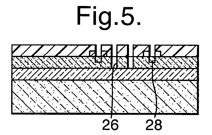
- slots or holes 22 are extended through layer 16 to form deep slots or holes 26 exposing insulator layer 14.
- grooves 28 are partially etched through layer 16.
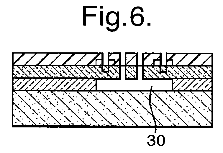
- a wet etch process is used to remove buried material from under semi-conductor layer 16 to form a hollow chamber 30.
- Suitable wet etchants include hydrofluoric acid and/or other liquids that can be used for etching insulation layer 14, but which do not appreciably etch layers 12 or 16.
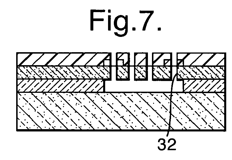
- a third DRIE step is performed to remove the remaining silicon under groove pattern 28, and create a separation or gap pattern 32 that defines the moveable component of a resulting MEMS structure.
- a conventional stripping material suitable for etching or otherwise removing photoresist material 20 can be employed to provide a finished device as shown in Fig. 8, in which the separation pattern 32 is completely defined by a dry etching process that is not susceptible to stiction problems normally associated with wet etching techniques.
Landscapes
- Engineering & Computer Science (AREA)
- Manufacturing & Machinery (AREA)
- Microelectronics & Electronic Packaging (AREA)
- Weting (AREA)
- Micromachines (AREA)
Abstract


Description
- This invention relates to a method of making a microelectromechanical system (MEMS) having a moveable component defined by a gap pattern in the semiconductor layer of a silicon-on-insulator (SOI) wafer.
- Microelectromechanical systems (MEMS) are being utilized in a variety of micro-sensor applications, with specific applications including accelerometers having a component that is moveable with respect to the main body or substrate of the device when subjected to acceleration, whereby a resulting change in a capacitive gap is used to generate an electrical output that can be correlated to the magnitude and/or direction of the acceleration. The MEMS device should be fabricated to form a functional element in a semiconductor wafer having an overall structure of small dimensions.
- MEMS fabrication processes commonly use a release technique to free the moveable component of the MEMS structure from the substrate or underlying films to allow the structure to freely move. The most common release method is to remove an oxide film from under a poly-silicon or silicon device layer using a wet etch technique. The use of a wet etch leads to stiction, which occurs when the moveable component contacts another surface of the device and becomes permanently or temporarily bonded to the other surface.
- Attempts to overcome the stiction problem associated with the use of wet etching have involved methods for removing the liquid etchant by alcohol displacement and subsequent evaporation. These techniques require additional steps, time and equipment, and therefore add significantly to the overall manufacturing cost.
- Recently, MEMS devices have been produced using deep reactive ion etching (DRIE) of silicon-on-insulator (SOI) wafers. This technique is used to remove material from the silicon device layer until the buried oxide layer is reached. The buried oxide layer is then removed with a wet etch technique or with vapor phase hydrofluoric acid (HF) etching. The wet etch technique results in stiction. The HF vapor process eliminates stiction but attacks most common semiconductor films.
- In this invention, a plurality of DRIE etching steps at different depths are used to allow a buried oxide layer of an SOI wafer to be exposed in selected areas before the entire moveable component of a resulting MEMS device is freed for movement. This method allows a wet release technique to be used to remove the buried oxide layer without developing stiction problems, since the structure that will eventually constitute the moveable component remains rigidly connected (i.e., remains immoveable) during the wet etching step. An additional DRIE etching step is used after the wet etching step to free the moveable component via a dry process.
- These and other features, advantages and objects of the present invention will be further understood and appreciated by those skilled in the art by reference to the following specification, claims and appended drawings.
-
- Fig. 1 is a schematic cross section of an SOI wafer suitable for use in preparing a MEMS structure in accordance with the methods of the invention.
- Figs. 2-7 show intermediate structures developed during a process in accordance with the invention.
- Fig. 8 shows a completed MEMS structure using a method in accordance with the invention.
- Shown in Fig. 1 is a silicon-on-insulator (SOI) wafer 10 from which a MEMS device can be fabricated employing the methods of the invention. SOI
wafer 10 is a layered device including a substrate orbase layer 12, which may be either electrically conductive or non-conductive. Suitable materials forbase layer 12 include silicon, crystalline sapphire, crystalline silicon, polycrystalline silicon, silicon carbide, alumina, alumina nitride, and gallium, arsenide. For accelerometer devices, it is usually desirable that thebase layer 12 is silicon. This ensures that the thermal and mechanical properties ofbase layer 12 and the MEMS structure fabricated from the other layers of the SOI are sufficiently similar to make processing easier and eliminate the possibility of undesirable thermally induced stresses, either during fabrication or use of the device. - Immediately
adjacent base layer 12 is an electrically non-conductive or insulative layer 14. Layer 14 is typically silicon dioxide or silicon nitride. - Adjacent insulator layer 14 is an electrically
semi-conductive layer 16, such as a phosphorus-doped or arsenic-doped silicon layer of material. - SOI wafers are well known in the art of fabricating MEMS structures, and are commercially available from several different sources.
Layer 16 is typically formed by bonding a substrate to layer 14 followed by grinding, capping, or polishing to control the thickness. Layer 14 is typically prepared by thermal oxidation, chemical vapor deposition (CVD), physical vapor deposition (PVD), plasma enhanced physical vapor deposition (PEPVD), or other well known techniques. The thickness oflayers layer 12 is from about 350 to 750 microns. The typical thickness for layer 14 is 1-3 µm, and the typical thickness forlayer 16 is 1-100 µm. - In a first step of a process in accordance with the invention, an etch inhibiting material 18 (Fig. 2) is deposited on the exposed surface of
layer 16 in a desired pattern generally corresponding with a separation pattern that defines a moveable component of a MEMS structure. Etched inhibitingmaterial 18 is any suitable material that will resist DRIE. SuitableDRIE inhibiting materials 18 include thin film oxides or nitrides such as silicon dioxide, which can be deposited on selected exposed surfaces oflayer 16 in a desired pattern using PVD, CVD, PEPVD or other suitable techniques. - Next, a
photoresist mask 20, which defines the shape of the moving component of the MEMS structure is patterned ontolayer 16. Suitable photoresist materials that can be patterned onto a surface oflayer 16 are well known in the art and commercially available. Similarly, suitable techniques of depositing a photoresist mask in a desired pattern on a surface are well known in the art and do not, of themselves, constitute a novel feature of the invention. - As can be seen in Fig. 3,
photoresist mask 20 exposesDRIE inhibiting material 18 at strategically selected locations, and also exposeslayer 16 at selected location overlying a portion of layer 14 that will be subsequently removed by wet etching to form a hollow chamber over which the moveable component will be supported. - DRIE is used to partially etch through the
SOI device layer 16 to form slots orholes 22. However, there is not any etching that takes place where DRIE inhibitingmaterial 18 is located. - After slots or
holes 22 have been formed, an etch process (e.g., HF etching) is used for removing exposedDRIE inhibiting material 18 and exposing theunderlying layer 16 as shown in Fig. 4. Suitable etchants are those that will etch material 18 (typically silicon dioxide), but will not appreciably etch layer 16 (typically silicon). The resulting intermediate structure of Fig. 4 includes at least one hole orslot 22 etched partially throughlayer 16, and aphotoresist mask 20 exposing slot orhole 22 and selected surfaces oflayer 16 for a subsequent DRIE step. - Upon further DRIE, slots or
holes 22 are extended throughlayer 16 to form deep slots orholes 26 exposing insulator layer 14. At the same time,grooves 28 are partially etched throughlayer 16. - With slots or
holes 26 exposing the surface of insulator layer 14 (e.g., metal oxide or metal nitride), a wet etch process is used to remove buried material from undersemi-conductor layer 16 to form ahollow chamber 30. Suitable wet etchants include hydrofluoric acid and/or other liquids that can be used for etching insulation layer 14, but which do not appreciably etchlayers - After the wet etch of layer 14 has been completed, and the etchant has been removed, a third DRIE step is performed to remove the remaining silicon under
groove pattern 28, and create a separation orgap pattern 32 that defines the moveable component of a resulting MEMS structure. - A conventional stripping material suitable for etching or otherwise removing
photoresist material 20 can be employed to provide a finished device as shown in Fig. 8, in which theseparation pattern 32 is completely defined by a dry etching process that is not susceptible to stiction problems normally associated with wet etching techniques. - The above description is considered that of the preferred embodiments only. Modifications of the invention will occur to those skilled in the art and to those who make or use the invention. Therefore, it is understood that the embodiments shown in the drawings and described above are merely for illustrative purposes and not intended to limit the scope of the invention, which is defined by the following claims as interpreted according to the principles of patent law, including the doctrine of equivalents.
Claims (1)
- A process for making a microelectromechanical system having a moveable component defined by a patterned gap in a semiconductor layer of a silicon-on-insulator wafer, wherein the moveable component is integrally supported by the semiconductor layer above a hollow chamber defined in an insulator layer of the silicon-on-insulator wafer, comprising:providing a silicon-on-insulator wafer (10) having a semiconductor layer (16) adjacent an insulator layer (14);depositing an etch inhibiting material (18) on the semiconductor layer (16) in a desired pattern generally corresponding with a gap pattern that defines a moveable component of the device, the etch inhibiting material (18) being resistant to deep reactive ion etching;patterning a photoresist mask (20) over the semiconductor layer (16), the photoresist mask (20) having a pattern that exposes a portion of the etch inhibiting material (18), and also exposes the semiconductor layer (16) at selected locations overlying a portion of the insulator layer (14) that is to be removed;deep reactive ion etching to partially etch openings (22) through the semiconductor layer;wet etching to remove the exposed etch inhibiting material (18);deep reactive ion etching to extend the partially etched semiconductor openings (22) through the semiconductor layer (16) and expose the insulator layer (14), and at the same time partially etch a groove pattern (28) into the semiconductor layer (16) which corresponds with the desired gap pattern (32) defining a moveable component;wet etching a portion of the insulator layer (14) to develop a hollow chamber (30) underlying the desired moveable component; and deep reactive ion etching to remove the remaining semiconductor material (16) under the groove pattern (28) to develop a gap pattern (32) that defines the moveable component.
Applications Claiming Priority (1)
| Application Number | Priority Date | Filing Date | Title |
|---|---|---|---|
| US11/151,680 US7160751B2 (en) | 2005-06-13 | 2005-06-13 | Method of making a SOI silicon structure |
Publications (2)
| Publication Number | Publication Date |
|---|---|
| EP1734000A2 true EP1734000A2 (en) | 2006-12-20 |
| EP1734000A3 EP1734000A3 (en) | 2011-10-12 |
Family
ID=36992495
Family Applications (1)
| Application Number | Title | Priority Date | Filing Date |
|---|---|---|---|
| EP06076128A Withdrawn EP1734000A3 (en) | 2005-06-13 | 2006-05-30 | Method of making a soi silicon structure |
Country Status (2)
| Country | Link |
|---|---|
| US (1) | US7160751B2 (en) |
| EP (1) | EP1734000A3 (en) |
Families Citing this family (4)
| Publication number | Priority date | Publication date | Assignee | Title |
|---|---|---|---|---|
| US7785913B2 (en) * | 2006-02-23 | 2010-08-31 | Innovative Micro Technology | System and method for forming moveable features on a composite substrate |
| US8057690B2 (en) * | 2009-03-11 | 2011-11-15 | Honeywell International Inc. | Single silicon-on-insulator (SOI) wafer accelerometer fabrication |
| CN102367165B (en) * | 2011-08-31 | 2015-01-21 | 华东光电集成器件研究所 | Method for interconnecting electrodes of MEMS (micro electro mechanical system) device based on SOI (silicon-on-insulator) |
| US8648432B2 (en) * | 2011-11-28 | 2014-02-11 | Texas Instruments Deutschland Gmbh | Fully embedded micromechanical device, system on chip and method for manufacturing the same |
Citations (1)
| Publication number | Priority date | Publication date | Assignee | Title |
|---|---|---|---|---|
| US20040200281A1 (en) | 2003-04-11 | 2004-10-14 | Kenny Thomas W. | Ultra-miniature accelerometers |
Family Cites Families (4)
| Publication number | Priority date | Publication date | Assignee | Title |
|---|---|---|---|---|
| US5658698A (en) * | 1994-01-31 | 1997-08-19 | Canon Kabushiki Kaisha | Microstructure, process for manufacturing thereof and devices incorporating the same |
| US6815243B2 (en) * | 2001-04-26 | 2004-11-09 | Rockwell Automation Technologies, Inc. | Method of fabricating a microelectromechanical system (MEMS) device using a pre-patterned substrate |
| US6660564B2 (en) * | 2002-01-25 | 2003-12-09 | Sony Corporation | Wafer-level through-wafer packaging process for MEMS and MEMS package produced thereby |
| US6916728B2 (en) * | 2002-12-23 | 2005-07-12 | Freescale Semiconductor, Inc. | Method for forming a semiconductor structure through epitaxial growth |
-
2005
- 2005-06-13 US US11/151,680 patent/US7160751B2/en not_active Expired - Lifetime
-
2006
- 2006-05-30 EP EP06076128A patent/EP1734000A3/en not_active Withdrawn
Patent Citations (1)
| Publication number | Priority date | Publication date | Assignee | Title |
|---|---|---|---|---|
| US20040200281A1 (en) | 2003-04-11 | 2004-10-14 | Kenny Thomas W. | Ultra-miniature accelerometers |
Also Published As
| Publication number | Publication date |
|---|---|
| EP1734000A3 (en) | 2011-10-12 |
| US20060281214A1 (en) | 2006-12-14 |
| US7160751B2 (en) | 2007-01-09 |
Similar Documents
| Publication | Publication Date | Title |
|---|---|---|
| EP0683921B1 (en) | Microstructures and single mask, single-crystal process for fabrication thereof | |
| US5426070A (en) | Microstructures and high temperature isolation process for fabrication thereof | |
| US7932118B2 (en) | Method of producing mechanical components of MEMS or NEMS structures made of monocrystalline silicon | |
| JP5602761B2 (en) | Micro-electromechanical system device having separated microstructure and manufacturing method thereof | |
| US7898046B2 (en) | Microelectromechanical systems encapsulation process | |
| US6887732B2 (en) | Microstructure devices, methods of forming a microstructure device and a method of forming a MEMS device | |
| US6440766B1 (en) | Microfabrication using germanium-based release masks | |
| JP2002355800A (en) | Method for producing anti-adhesion microstructure | |
| WO2005092782A1 (en) | Single crystal silicon sensor with additional layer and method of producing the same | |
| EP1433199B1 (en) | Method for forming a cavity structure in an soi substrate and cavity structure formed in an soi substrate | |
| KR100373739B1 (en) | Method for Fabrication of Electrostatic Vertical Actuators Using One Single-crystalline Silicon Wafer | |
| JPH11261079A (en) | Semiconductor element and its manufacture | |
| US9070699B2 (en) | Micromachined structures | |
| US6544863B1 (en) | Method of fabricating semiconductor wafers having multiple height subsurface layers | |
| US20040159629A1 (en) | MEM device processing with multiple material sacrificial layers | |
| US20060278942A1 (en) | Antistiction MEMS substrate and method of manufacture | |
| US7160751B2 (en) | Method of making a SOI silicon structure | |
| EP1186002A4 (en) | IC COMPATIBLE PARYLENE MEMS TECHNOLOGY AND ITS APPLICATION IN INTEGRATED SENSORS | |
| US6815243B2 (en) | Method of fabricating a microelectromechanical system (MEMS) device using a pre-patterned substrate | |
| US6790699B2 (en) | Method for manufacturing a semiconductor device | |
| CN102120561B (en) | Method for forming wafer through hole | |
| US9000556B2 (en) | Lateral etch stop for NEMS release etch for high density NEMS/CMOS monolithic integration | |
| JP5382937B2 (en) | Etching method with improved control of feature critical dimension at the bottom of thick film | |
| US9156685B2 (en) | Method for the prevention of suspended silicon structure etching during reactive ion etching | |
| CN112158796A (en) | Preparation method of silicon wafer with rough surface and silicon wafer |
Legal Events
| Date | Code | Title | Description |
|---|---|---|---|
| PUAI | Public reference made under article 153(3) epc to a published international application that has entered the european phase |
Free format text: ORIGINAL CODE: 0009012 |
|
| AK | Designated contracting states |
Kind code of ref document: A2 Designated state(s): AT BE BG CH CY CZ DE DK EE ES FI FR GB GR HU IE IS IT LI LT LU LV MC NL PL PT RO SE SI SK TR |
|
| AX | Request for extension of the european patent |
Extension state: AL BA HR MK YU |
|
| PUAL | Search report despatched |
Free format text: ORIGINAL CODE: 0009013 |
|
| AK | Designated contracting states |
Kind code of ref document: A3 Designated state(s): AT BE BG CH CY CZ DE DK EE ES FI FR GB GR HU IE IS IT LI LT LU LV MC NL PL PT RO SE SI SK TR |
|
| AX | Request for extension of the european patent |
Extension state: AL BA HR MK YU |
|
| RIC1 | Information provided on ipc code assigned before grant |
Ipc: B81C 1/00 20060101AFI20110908BHEP |
|
| 17P | Request for examination filed |
Effective date: 20120412 |
|
| AKX | Designation fees paid |
Designated state(s): AT BE BG CH CY CZ DE DK EE ES FI FR GB GR HU IE IS IT LI LT LU LV MC NL PL PT RO SE SI SK TR |
|
| STAA | Information on the status of an ep patent application or granted ep patent |
Free format text: STATUS: THE APPLICATION HAS BEEN WITHDRAWN |
|
| 18W | Application withdrawn |
Effective date: 20170510 |