EP1732142A1 - Si Solarzelle und ihr Herstellungsverfahren - Google Patents
Si Solarzelle und ihr Herstellungsverfahren Download PDFInfo
- Publication number
- EP1732142A1 EP1732142A1 EP05105081A EP05105081A EP1732142A1 EP 1732142 A1 EP1732142 A1 EP 1732142A1 EP 05105081 A EP05105081 A EP 05105081A EP 05105081 A EP05105081 A EP 05105081A EP 1732142 A1 EP1732142 A1 EP 1732142A1
- Authority
- EP
- European Patent Office
- Prior art keywords
- type
- solar cell
- rear side
- body layer
- doping
- Prior art date
- Legal status (The legal status is an assumption and is not a legal conclusion. Google has not performed a legal analysis and makes no representation as to the accuracy of the status listed.)
- Withdrawn
Links
- 238000004519 manufacturing process Methods 0.000 title claims abstract description 12
- XUIMIQQOPSSXEZ-UHFFFAOYSA-N Silicon Chemical compound [Si] XUIMIQQOPSSXEZ-UHFFFAOYSA-N 0.000 claims abstract description 54
- 229910052710 silicon Inorganic materials 0.000 claims abstract description 54
- 239000010703 silicon Substances 0.000 claims abstract description 54
- 238000009792 diffusion process Methods 0.000 claims description 41
- ZOXJGFHDIHLPTG-UHFFFAOYSA-N Boron Chemical compound [B] ZOXJGFHDIHLPTG-UHFFFAOYSA-N 0.000 claims description 34
- 229910052796 boron Inorganic materials 0.000 claims description 33
- 238000000034 method Methods 0.000 claims description 30
- 238000002161 passivation Methods 0.000 claims description 30
- 239000002019 doping agent Substances 0.000 claims description 18
- VYPSYNLAJGMNEJ-UHFFFAOYSA-N Silicium dioxide Chemical compound O=[Si]=O VYPSYNLAJGMNEJ-UHFFFAOYSA-N 0.000 claims description 8
- 229910021417 amorphous silicon Inorganic materials 0.000 claims description 6
- 239000007788 liquid Substances 0.000 claims description 6
- 229910052681 coesite Inorganic materials 0.000 claims description 4
- 229910052906 cristobalite Inorganic materials 0.000 claims description 4
- 239000000377 silicon dioxide Substances 0.000 claims description 4
- 229910052682 stishovite Inorganic materials 0.000 claims description 4
- 229910052905 tridymite Inorganic materials 0.000 claims description 4
- -1 SiN Chemical class 0.000 claims description 3
- 150000004767 nitrides Chemical class 0.000 claims description 3
- 235000012431 wafers Nutrition 0.000 description 51
- 230000015556 catabolic process Effects 0.000 description 18
- 238000006731 degradation reaction Methods 0.000 description 18
- 230000008569 process Effects 0.000 description 18
- BHEPBYXIRTUNPN-UHFFFAOYSA-N hydridophosphorus(.) (triplet) Chemical compound [PH] BHEPBYXIRTUNPN-UHFFFAOYSA-N 0.000 description 16
- 238000005259 measurement Methods 0.000 description 16
- 238000005215 recombination Methods 0.000 description 16
- 230000006798 recombination Effects 0.000 description 16
- 230000008901 benefit Effects 0.000 description 10
- 239000002800 charge carrier Substances 0.000 description 10
- 238000005286 illumination Methods 0.000 description 10
- 230000015572 biosynthetic process Effects 0.000 description 8
- 239000000463 material Substances 0.000 description 8
- 238000010304 firing Methods 0.000 description 7
- 238000005275 alloying Methods 0.000 description 5
- 238000013459 approach Methods 0.000 description 5
- 230000004044 response Effects 0.000 description 5
- 238000010521 absorption reaction Methods 0.000 description 4
- 239000011248 coating agent Substances 0.000 description 4
- 238000000576 coating method Methods 0.000 description 4
- 238000005530 etching Methods 0.000 description 4
- 230000007246 mechanism Effects 0.000 description 4
- 229910052782 aluminium Inorganic materials 0.000 description 3
- 229910021419 crystalline silicon Inorganic materials 0.000 description 3
- 238000000151 deposition Methods 0.000 description 3
- 230000008021 deposition Effects 0.000 description 3
- 230000000694 effects Effects 0.000 description 3
- 239000012071 phase Substances 0.000 description 3
- 238000007650 screen-printing Methods 0.000 description 3
- 229910000838 Al alloy Inorganic materials 0.000 description 2
- 239000004411 aluminium Substances 0.000 description 2
- XAGFODPZIPBFFR-UHFFFAOYSA-N aluminium Chemical compound [Al] XAGFODPZIPBFFR-UHFFFAOYSA-N 0.000 description 2
- 239000000969 carrier Substances 0.000 description 2
- 230000003247 decreasing effect Effects 0.000 description 2
- 238000009826 distribution Methods 0.000 description 2
- 239000007789 gas Substances 0.000 description 2
- 238000010438 heat treatment Methods 0.000 description 2
- 230000006872 improvement Effects 0.000 description 2
- 238000002347 injection Methods 0.000 description 2
- 239000007924 injection Substances 0.000 description 2
- 239000004065 semiconductor Substances 0.000 description 2
- 238000000926 separation method Methods 0.000 description 2
- 229910052709 silver Inorganic materials 0.000 description 2
- 229910021364 Al-Si alloy Inorganic materials 0.000 description 1
- 238000002231 Czochralski process Methods 0.000 description 1
- GYHNNYVSQQEPJS-UHFFFAOYSA-N Gallium Chemical compound [Ga] GYHNNYVSQQEPJS-UHFFFAOYSA-N 0.000 description 1
- BQCADISMDOOEFD-UHFFFAOYSA-N Silver Chemical compound [Ag] BQCADISMDOOEFD-UHFFFAOYSA-N 0.000 description 1
- LBZRRXXISSKCHV-UHFFFAOYSA-N [B].[O] Chemical compound [B].[O] LBZRRXXISSKCHV-UHFFFAOYSA-N 0.000 description 1
- 230000002411 adverse Effects 0.000 description 1
- 229910045601 alloy Inorganic materials 0.000 description 1
- 239000000956 alloy Substances 0.000 description 1
- PNEYBMLMFCGWSK-UHFFFAOYSA-N aluminium oxide Inorganic materials [O-2].[O-2].[O-2].[Al+3].[Al+3] PNEYBMLMFCGWSK-UHFFFAOYSA-N 0.000 description 1
- 238000004458 analytical method Methods 0.000 description 1
- QVGXLLKOCUKJST-UHFFFAOYSA-N atomic oxygen Chemical compound [O] QVGXLLKOCUKJST-UHFFFAOYSA-N 0.000 description 1
- 230000004888 barrier function Effects 0.000 description 1
- 238000006243 chemical reaction Methods 0.000 description 1
- 230000002301 combined effect Effects 0.000 description 1
- 150000001875 compounds Chemical class 0.000 description 1
- 239000013078 crystal Substances 0.000 description 1
- 230000007547 defect Effects 0.000 description 1
- 238000011161 development Methods 0.000 description 1
- 238000005516 engineering process Methods 0.000 description 1
- 238000002474 experimental method Methods 0.000 description 1
- 230000002349 favourable effect Effects 0.000 description 1
- 239000000945 filler Substances 0.000 description 1
- 229910052733 gallium Inorganic materials 0.000 description 1
- 238000009776 industrial production Methods 0.000 description 1
- 238000011031 large-scale manufacturing process Methods 0.000 description 1
- 239000007791 liquid phase Substances 0.000 description 1
- 230000007774 longterm Effects 0.000 description 1
- 229910052751 metal Inorganic materials 0.000 description 1
- 239000002184 metal Substances 0.000 description 1
- 230000004048 modification Effects 0.000 description 1
- 238000012986 modification Methods 0.000 description 1
- CMWTZPSULFXXJA-VIFPVBQESA-N naproxen Chemical compound C1=C([C@H](C)C(O)=O)C=CC2=CC(OC)=CC=C21 CMWTZPSULFXXJA-VIFPVBQESA-N 0.000 description 1
- 230000003287 optical effect Effects 0.000 description 1
- 239000001301 oxygen Substances 0.000 description 1
- 229910052760 oxygen Inorganic materials 0.000 description 1
- 239000002245 particle Substances 0.000 description 1
- 238000012545 processing Methods 0.000 description 1
- 230000009467 reduction Effects 0.000 description 1
- 238000011160 research Methods 0.000 description 1
- 230000002441 reversible effect Effects 0.000 description 1
- 238000005204 segregation Methods 0.000 description 1
- 239000004332 silver Substances 0.000 description 1
- 239000007790 solid phase Substances 0.000 description 1
- 239000000243 solution Substances 0.000 description 1
- 238000012421 spiking Methods 0.000 description 1
- 239000000725 suspension Substances 0.000 description 1
Images


Classifications
-
- H—ELECTRICITY
- H01—ELECTRIC ELEMENTS
- H01L—SEMICONDUCTOR DEVICES NOT COVERED BY CLASS H10
- H01L31/00—Semiconductor devices sensitive to infrared radiation, light, electromagnetic radiation of shorter wavelength or corpuscular radiation and specially adapted either for the conversion of the energy of such radiation into electrical energy or for the control of electrical energy by such radiation; Processes or apparatus specially adapted for the manufacture or treatment thereof or of parts thereof; Details thereof
- H01L31/04—Semiconductor devices sensitive to infrared radiation, light, electromagnetic radiation of shorter wavelength or corpuscular radiation and specially adapted either for the conversion of the energy of such radiation into electrical energy or for the control of electrical energy by such radiation; Processes or apparatus specially adapted for the manufacture or treatment thereof or of parts thereof; Details thereof adapted as photovoltaic [PV] conversion devices
- H01L31/06—Semiconductor devices sensitive to infrared radiation, light, electromagnetic radiation of shorter wavelength or corpuscular radiation and specially adapted either for the conversion of the energy of such radiation into electrical energy or for the control of electrical energy by such radiation; Processes or apparatus specially adapted for the manufacture or treatment thereof or of parts thereof; Details thereof adapted as photovoltaic [PV] conversion devices characterised by potential barriers
- H01L31/068—Semiconductor devices sensitive to infrared radiation, light, electromagnetic radiation of shorter wavelength or corpuscular radiation and specially adapted either for the conversion of the energy of such radiation into electrical energy or for the control of electrical energy by such radiation; Processes or apparatus specially adapted for the manufacture or treatment thereof or of parts thereof; Details thereof adapted as photovoltaic [PV] conversion devices characterised by potential barriers the potential barriers being only of the PN homojunction type, e.g. bulk silicon PN homojunction solar cells or thin film polycrystalline silicon PN homojunction solar cells
- H01L31/0684—Semiconductor devices sensitive to infrared radiation, light, electromagnetic radiation of shorter wavelength or corpuscular radiation and specially adapted either for the conversion of the energy of such radiation into electrical energy or for the control of electrical energy by such radiation; Processes or apparatus specially adapted for the manufacture or treatment thereof or of parts thereof; Details thereof adapted as photovoltaic [PV] conversion devices characterised by potential barriers the potential barriers being only of the PN homojunction type, e.g. bulk silicon PN homojunction solar cells or thin film polycrystalline silicon PN homojunction solar cells double emitter cells, e.g. bifacial solar cells
-
- H—ELECTRICITY
- H01—ELECTRIC ELEMENTS
- H01L—SEMICONDUCTOR DEVICES NOT COVERED BY CLASS H10
- H01L31/00—Semiconductor devices sensitive to infrared radiation, light, electromagnetic radiation of shorter wavelength or corpuscular radiation and specially adapted either for the conversion of the energy of such radiation into electrical energy or for the control of electrical energy by such radiation; Processes or apparatus specially adapted for the manufacture or treatment thereof or of parts thereof; Details thereof
- H01L31/18—Processes or apparatus specially adapted for the manufacture or treatment of these devices or of parts thereof
- H01L31/1804—Processes or apparatus specially adapted for the manufacture or treatment of these devices or of parts thereof comprising only elements of Group IV of the Periodic Table
-
- Y—GENERAL TAGGING OF NEW TECHNOLOGICAL DEVELOPMENTS; GENERAL TAGGING OF CROSS-SECTIONAL TECHNOLOGIES SPANNING OVER SEVERAL SECTIONS OF THE IPC; TECHNICAL SUBJECTS COVERED BY FORMER USPC CROSS-REFERENCE ART COLLECTIONS [XRACs] AND DIGESTS
- Y02—TECHNOLOGIES OR APPLICATIONS FOR MITIGATION OR ADAPTATION AGAINST CLIMATE CHANGE
- Y02E—REDUCTION OF GREENHOUSE GAS [GHG] EMISSIONS, RELATED TO ENERGY GENERATION, TRANSMISSION OR DISTRIBUTION
- Y02E10/00—Energy generation through renewable energy sources
- Y02E10/50—Photovoltaic [PV] energy
- Y02E10/547—Monocrystalline silicon PV cells
-
- Y—GENERAL TAGGING OF NEW TECHNOLOGICAL DEVELOPMENTS; GENERAL TAGGING OF CROSS-SECTIONAL TECHNOLOGIES SPANNING OVER SEVERAL SECTIONS OF THE IPC; TECHNICAL SUBJECTS COVERED BY FORMER USPC CROSS-REFERENCE ART COLLECTIONS [XRACs] AND DIGESTS
- Y02—TECHNOLOGIES OR APPLICATIONS FOR MITIGATION OR ADAPTATION AGAINST CLIMATE CHANGE
- Y02P—CLIMATE CHANGE MITIGATION TECHNOLOGIES IN THE PRODUCTION OR PROCESSING OF GOODS
- Y02P70/00—Climate change mitigation technologies in the production process for final industrial or consumer products
- Y02P70/50—Manufacturing or production processes characterised by the final manufactured product
Definitions
- the present invention relates to a solar cell and to a method of manufacturing a solar cell.
- Conventional silicon (Si) based solar cells comprise a base layer of crystalline Si doped with boron. At the side facing the sun during normal operation (the front side), an n-doped layer is provided e.g. by diffusion of phosphorous into the base layer. This so-called emitter layer forms a p/n-junction with the p-doped base layer. Front and rear side contacts are arranged that are in electrical connection with the n-doped layer and the p-doped base layer, respectively, to withdraw a photocurrent from both sides of the p/n-junction.
- a known problem in such solar cells is degradation of the boron doped base layer, which is also referred to as light induced degradation (LID).
- LID light induced degradation
- the degradation adversely affects the minority carrier lifetime, i.e. electron lifetime in the boron (p) doped base layer, and is observed in both monocrystalline as well as in multi- or polycrystalline materials.
- Ga doped Si shows a much better stability indeed, this is not seen as a practical alternative for commercial cell production as Ga-doped crystalline Silicon is much more difficult to grow in a Czochralski process due to a difference in segregation coefficients.
- Another alternative that has been considered is to reverse the doping of the base layer and the front side emitter layer, so that an n-type base layer of Phosphorous doping is used, at the front side of which a p-doped emitter layer is provided that forms a p/n-junction with the base layer.
- the base layer shows much better stability than boron-doped base layers in conventional cells, however degradation mechanisms of the front surface passivation of the p-type front emitter are observed here.
- the invention provides a solar cell comprising
- the non-alloyed p-type doped region is a doping region obtained by diffusion of a dopant into the base layer, in particular by diffusion from a p-type dopant from a liquid that is applied to the rear side.
- the p-type dopant is Boron, but other dopants are also possible.
- an Al alloy is opaque, whereas a doping region as obtained by diffusion only without alloying is transparent. This allows in a special embodiment to allow a maximum of light to be received as well through the rear side, such as diffuse or reflected light. In principle only the rear contacts provide shading.
- n-type Si as body layer overcomes the degradation problem of conventional solar cells with a boron doped body layer, and at the same time the invention circumvents the use of a p-doped front layer that can degrade as well.
- the placement of the p/n-junction at the rear side of the cell has the further advantage that the photocurrent maximised since light cannot be unproductively absorbed in a front-side emitter, in particular in the so-called dead zone of such an emitter. This maximises in particular the contribution of short wavelength light to the photocurrent, because such light is predominantly absorbed close to the front side, whereas longer wavelength light penetrates deeper into the cell.
- the cell further comprises a n+ doped region between the front contact and the n-type silicon body layer.
- n+ doped regions form a n+/n junction with the base layer underneath the front contacts, and thereby create a driving force for photogenerated minority carriers away from the front contact.
- This can also be referred to as creating a 'front surface field', using similar terminology as the well-known 'back surface field' created by a p+/p junction at the rear side of a conventional cell.
- a further advantage of arranging an n+ doped region underneath the front contact is that a better electrical connection is obtained, in particular when screen-printed/fired front contacts are used. In this way a possible metal/semiconductor Schottky contact can be overcome by tunnelling.
- the n+ doped region is a shallow n+ doped region.
- the term shallow can refer to a relatively light n+ doping and/or to a doping that does not extend very deep, such as less than 1 micrometer, into the body layer.
- a shallow doping is preferred for minimizing recombination at the front surface.
- the doping is preferably just sufficient for a good electrical contact with the front contact.
- the front contact has a finger structure striking a compromise between minimum shading of the front surface and optimum withdrawal of photocurrent.
- the n+ doped region between the front contact and the body layer can extend over the entire or substantially all of the front surface, or it can only be arranged surrounding the front contact. In the latter case, the n+ doping on the front side suitably covers at the highest 200% of the front surface area that is covered by the front side contact, preferably at the highest 150%, more preferably 130% thereof. In this way, a selective front surface field can be obtained, wherein the n+ doping underneath the contacts can be chosen such that a sufficient front surface field is achieved and for good contacting is provided, but recombination at the front surface area not covered by the front contact can be minimized.
- n-type doping in particular at a level between that of the n+ region and that of the n-type Si body layer. This can be advantageous for example for optimum passivation of the front surface.
- the solar cell further suitably comprises a passivation layer at the front side, in order to minimize recombination losses at the front surface.
- the layer can preferably for example be an oxide such as SiO 2 , a nitride such as SiN, undoped amorphous silicon, or n+ doped amorphous silicon layer.
- the rear contact of the solar cell covers only part of the rear side. In this way, less material such as Ag or Al is required for the contacts, which could have the shape of a finger structure. Moreover it can be arranged that light can also be received through the rear side.
- the p-doped regions at the rear side can only be arranged between the rear-side contact and the n-doped body layer, i.e. immediately surrounding the rear side contacts but not in substantially all of the remaining area on the rear side that is not covered by the rear side contact. In this way recombination at the rear side can be minimized.
- the p-dopes region can cover for example 200% of the rear surface area that is covered by the rear contact, preferably at the highest 150%, more preferably 130% or less thereof. In a rear surface region between the p-doped region a weaker p-doping can be applied as well.
- the invention further provides a method of manufacturing a solar cell, the method comprising
- the solar cell 1 comprises a silicon body layer 3 of n-type bulk doping having a front side 6 and a rear side 7.
- the silicon body layer 3 is made from crystalline silicon, and can be of the mono-, multi- or polycrystalline type. Preferably, Czochralski grown Silicon is used.
- the thickness of the body layer can be typically between 10 and 400 ⁇ m, suitably between 100 and 300 ⁇ m, preferably between 150-250 ⁇ m.
- a suitable dopant is for example phosphorous.
- the doping level is generally in the range of 10 13 -10 18 atoms per cm 3 , typically in the order of 10 15 -10 16 .
- the doping is such that a resistivity higher than 0.5 and lower than 150 Ohm.cm is obtained, preferably higher than 1 and lower than 20, more preferably lower than 10 Ohm.cm.
- a p-doped layer 10 is arranged suitably such as discussed further below, and a p/n-junction 12 with the body layer is formed.
- the doping level of the p-region can be higher that what one would use at a front contact, since at the rear side that is away from the light-receiving front side there most of the light has already been absorbed and there is less risk for recombination.
- a typical surface resistivity for the p-doped region in the present invention is in the range of 3 Ohm/sq or higher and 60 Ohm/sq or lower, preferably 5 Ohm/sq and higher, preferably 50 Ohm/sq and lower, such as 6 Ohm/sq.
- Ohm/sq (equivalent to Ohm/square) is a commonly used parameter to characterized surface resistivity, which is also referred to as sheet resistivity.
- the depth of the p-emitter is typically in the range of 0.1-6 ⁇ m, when Boron diffusion from a liquid source is used typically 1-5 ⁇ m, often 1-3 ⁇ m.
- a rear side contact 15 is arranged in electrical connection with the p-doped layer 10.
- the rear side contact is shown covering a large part or substantially all of the rear side of the cell.
- screen-printed front side contacts 16 are provided in electrical connection with the n-type silicon body layer.
- the front side contacts form part of a finger structure 19 such as sketched in top view in Figure 2 covering typically around 10% of the front service when screen printed contacts are used.
- the electrical connection is provided via a shallow n+ doped layer 17 on the front side 6, i.e. between the front contact and the n-type silicon body layer.
- the n+ doped layer can have a surface resistivity of typically between 40 and 250 Ohm/sq, preferably 50 Ohm/sq and higher, more preferably 80 Ohm/sq and higher, in particular 120 Ohm/sq and higher, such as between 130 and 200 Ohm/sq.
- the n+ doping level is typically less than 4 ⁇ m deep, in particular 3 ⁇ m or less.
- the layer typically exhibits a concentration profile of n-dopant, which can be determined by SIMS, e.g. having a surface concentration of 6.10 21 atoms/cm 3 down to 10 18 at 2-3 ⁇ m into the material.
- the front surface is further provided with a passivation layer 18.
- the passivation layer can for example be an oxide such as SiO 2 a nitride such as SiN, undoped amorphous silicon, or mildly n+ doped amorphous silicon layer, which can be arranged using methods known in the art. It is a further advantage of the present invention that n or n+ doped layers can generally easier and better be passivated than p or p+ doped layers.
- An advantage of using SiN as passivation layer is that it has intrinsic charges.
- an anti-reflection coating is provided as known in the art.
- the front side 6 faces the sun and light is received through the area of the front surface that is not covered by the front contact 16. Light is absorbed predominantly in the n-doped body layer 3, and excess hole-electron pairs are created.
- the holes form minority charge carriers in the n-type material and travel towards the rear side over the p/n-junction 12 where they become majority carriers in the p-layer that are withdrawn at the rear side contact thereby providing photocurrent.
- the photogenerated excess electrons are prevented from diffusing to the front contacts by the field exerted by the n+/n junction leading between the body layer 3 and the p+ layer 18.
- FIG. 3 showing a second embodiment of a solar cell 31 according to the invention.
- Cell 31 differs from cell 1 of Figure 1 in that the rear contacts 35 are arranged in a finger structure covering only part of the rear side, e.g. similar to that of Figure 2. A typical coverage is in the range of 10-40% of the rear surface. Between the fingers a passivation layer 34 is arranged, for which the same type of layers can be used as for the front side. If the cell is suitably arranged for operation such that reflected or diffracted light is received at the rear side not facing the sun, additional photocurrent can be created by photons absorbed predominantly in the body layer 3 from the rear side.
- Regions 38 of high n+ doping are arranged surrounding the front contacts 16, and regions 39 of weaker n+ doping in between front contact fingers, wherein the weaker n+ doping can be achieved by a doping concentration intermediate between that of the n-type body layer and that of the n+ doped regions 18, and/or in that regions 39 are shallower than regions 38.
- FIG. 4 showing a third embodiment of a solar cell 41 according to the invention.
- Cell 41 is similar to cell 31 of Figure 3, but in this case the front surface field is only provided by n+ doped regions 38, and the remainder of the front side of the body layer 3 is not provided with further doping in addition to the basic doping of the body layer.
- FIG. 5 showing a fourth embodiment of a solar cell 51 according to the invention.
- Cell 51 is similar to cell 41 of Figure 4, however the p doping at the rear side is only provided in regions 55 surrounding the rear contacts 35. In this way a maximum amount of, in particular short-wave, light that is received through the rear side of the cell can contribute to the generation of photocurrent.
- This embodiment allows an optimizing of the fractional rear surface area used for p-doped regions, independent of the area covered by rear side contacts. This is a further advantage over cells with Al alloyed rear contacts, in which the area of p-doped regions cannot be chosen larger than the area covered by opaque Aluminium, there Al serves both as dopant and provides the contacting structure.
- Light that is received through the rear side can be reflected light or diffuse light.
- a silicon body layer of n-type bulk doping typically a wafer in ⁇ 100> orientation that was sawed from a Cz grown and Phosphorous doped crystal, is provided. If desired a short, alkaline crystal-oriented etching can be used to texture the surface in order to improve the geometry of incidence of light in order to prevent reflection.
- Providing a non-alloyed p-type doped region is done by a process which introduces dopant, preferably boron, only by diffusion into the rear surface of the body layer.
- dopant preferably boron
- Several processes for boron diffusion are known in the art, including diffusion from the gas phase or from liquid and solid phases applied to the surface.
- a preferred process is that known for the making of a p+ back surface field on the rear side of conventional p-type cells. This process as well as prior art is described in USA patents No. 5899704 and 6096968 , which are incorporated by reference.
- a diffusion source layer that contains boron as a dopant is applied, e.g. spun, only onto the back of the n- doped silicon wafer.
- the diffusion source layer is one that contains boron and out of which the boron is thermally driven.
- the diffusion source layer is preferably applied by means of a boron doping resist. In addition to boron or its compounds, this resist contains powdery SiO 2 in a suspension. This doping resist is normally used for generating high dopings in power semiconductors. It may be applied in liquid form and may for example be spun on.
- a suitable doping liquid is Siodop (TM) of Merck. Then the wafer is treated in an atmosphere that contains oxygen at a temperature of 900 to 1200 degree centigrade, preferably between 1000 and 1100 degree C, to generate an oxide layer and to drive in the dopant.
- the oxide layer can be removed from the front surface, e.g. using HF, and optionally also the diffusion source layer and the oxide layer from the rear surface, followed by a diffusion of Phosphorous from the gas phase to form a front side n+ layer.
- a mask can be arranged on the front surface before removing the oxide layer, so that the oxide layer can be selectively etched away, followed by deep n-dopant (typically Phosphorous) diffusion into the body layer through the openings in the oxide layer. Then, the oxide layer can be fully removed, and if desired a shallow n-doping can be applied, this can be applied to the entire surface as the n+ regions will remain.
- n-dopant typically Phosphorous
- a mask can be applied to the oxide on the rear side and those p-doped regions can be etched away that are not desired, leaving the desired emitter structure in place.
- the desired emitter structure can be precisely adjusted in this way.
- a separation at the edge of the wafer may be performed, e.g. in a plasma.
- Front and rear side contacts are preferably screen-printed in an industrial production process, and contacting is done at elevated temperatures. These can be 700-800 degree centigrade, but lower temperatures are also possible.
- the squeegee paste for rear side contacts can contain silver particles, filler, oxides, and also an amount of Aluminium. It will be understood that at firing the paste in order to make electrical contact with the p region, a thin alloy might be formed at the interface between the p-doped region and the contact, but that the p-doped region itself towards the p/n junction is still a non-alloyed p-doped region.
- the front side contact is also suitably produced by screen printing and firing.
- Passivation and antireflection coating can be applied using known methods, before or after contact formation.
- a considerable advantage of the solar cell of the invention is that it can be produced with only minor adjustments of a known and industrially applied process for conventional p-type cells, and also using the advantages of that process as described in the cited US patents. Adjustments concern the adjustment of the doping to achieve desired sheet resistances.
- Bare wafers have been measured by the El(y)mat-method in order to determine the diffusion length LD of charge carriers in the wafer.
- This method uses a HF-solution in order to passivate the surface and to form a Schottky barrier on the rear side oft the wafer.
- This contact is used to extract minority charge carriers, generated by a laser operating at 680 nm that illuminates the wafer from the front side with a spot size of about 1 mm 2 . The extracted current can be used to determine LD.
- n-type wafers do not show a degradation, and whether LD of the bulk silicon is superior to p-type boron doped silicon
- El(y)mat measurements have been taken from a boron and phosphorous doped wafers before and after 50h illumination.
- Area averaged diffusion length LD on 125 x 125 mm 2 for various wafers was determined. It was found that the area average diffusion length decreased from 400 to 220 ⁇ m due to illumination of the boron wafer, but that the Phosphorous doped wafer had an stable LD of 440 ⁇ m before and after illumination.
- the wafer thickness is usually below 300 ⁇ m, the n-type wafers are suitable for fabricating a stable solar cells.
- the final solar cells have been investigated by current-voltage (I-V) and internal quantum efficiency (IQE) measurements.
- the quantum efficiency analysis has been performed by illumination of the front and rear side, respectively.
- Solar cells were manufactured from solar grade monocrystalline 125 mm x 125 mm Cz (Czochralski)- grown p and n-type silicon wafers as body layers, of about 250 ⁇ m thickness as sawn. After etch removal, texture etching was applied to the wafers. Three types of cells were manufactured and compared, conventional cells with p-doped body layer and front side p/n junction, n-type body layer cells with front p/n junction, and n-type body layer cells with rear p/n junction according to the invention.
- boron from a dopant source was diffused into the silicon.
- Boron diffusion for BSF formation in p-type silicon suitably gives a sheet resistance of e.g. below 20 Ohm/sq.
- a front side emitter on an n-type Si suitably has a sheet resistance of 50 Ohm/sq or above, otherwise recombination losses are too high.
- a phosphorous diffusion as used to arrange front side emitter for p-type silicon, and rear BSF for front contact n-type or front surface for n-type silicon.
- the Phosphorous diffusion process is conducted differently for p- and n-type silicon, in order to adopt the diffusion doping to the application, e.g. above 50 Ohm/sq for emitter formation for p-type Si wafers and below 20 Ohm/sq for BSF formation for n-type Si wafers.
- a weaker/shallower doping of the layer 17 is used as compared to a BSF, typically 50 Ohm/sq and higher.
- SiN was used in all cases as antireflection as well as surface passivation coating for n- and p-type silicon. Screen printing on the front and rear side is used for contact formation. The process sequences are in all cases similar except for the doping levels (sheet resistances) as discussed, and can be used on industrial scale.
- SIMS measurements on wafers that have been diffusion doped in parallel with the tested solar cells show a deep emitter profile of about 2 ⁇ m.
- the passivation seems not to be very effective, most of the charge carriers generated in the emitter recombine rather than separate within the p/n-junction.
- the blue response is significantly enhanced compared to a rear illuminated p-type cell, as the recombination in the BSF is even more enhanced than in the boron emitter of n-type cells due to lower boron doping.
- the red (long wavelength) response of the IQE measurements indicates a higher diffusion length for n-type compared to p-type silicon, as already measured on the bare wafers. Therefore LD is not drastically reduced after all the process steps, especially after the boron diffusion.
- the high LD observed in the Phosphorous doped wafers mainly supports this approach, as it is a pre-condition for rear junction solar cells. Additionally a uniform shallow boron emitter can be a challenge for boron diffusion with a dopant source. It is a further advantage of the present invention that this requirement for a higher efficient solar cell is avoided in a rear junction cell, as in this type of solar cell light doesn't have to transverse the deep and highly doped region.
- the quality of the p/n junction obtained with an boron diffusion process is much better than can be achieved in Al-alloyed emitters, which can be highly inhomogeneous, spiking and exhibit partly shunting, and the exact doping is difficult to control.
- the cell fabrication for rear junction n-type silicon is very similar to the cell fabrication of usual p-type solar cells described hereinbefore.
- the solar cell structure is shown in Fig. 1.
- the main difference compared to a p-type cell is, that the final solar cell has the p/n-junction on the rear side for n-type silicon solar cells.
- the incoming light has to pass the phosphorous diffused front region, that acts as a front surface field in a similar manner, than the BSF in p-type cell.
- the advantage to the FSF is that it is not as highly doped (sheet resistance 50 Ohm/sq and above) as a usual BSF (sheet resistance 20 Ohm/sq and below), minimising recombination in this layer.
- Table II summarises the results of non-optimised process conditions for n-type Si solar cells.
- Table II p-type n-type rear p/n junction diff. (%) ⁇ (%) 17.2 15.4 - 10.5 J SC (mA/cm 2 ) 35.5 32.3 - 9.0 V OC (mV) 619 621 + 0.0 FF (%) 78.3 76.9 - 1.8
- Fig. 7 shows IQE measurements on a front junction cell (curve a) and a rear junction cell (curve b) on the basis of an n-type body Si layer.
- the increase in the blue wavelength regime in curve b demonstrates the reduced recombination within the FSF compared to the recombination in the boron emitter of the front junction cell.
- This increased short wavelength response is responsible for the increase in J SC from 29.6 mA/cm 2 to 32.3 mA/cm 2 .
- the IQE characteristic of the rear junction cell shows a broad plateau between 500 and 900 nm at a value of slightly below 0.9 and is limited due to FSF recombination in the blue wavelength regime and due to finite absorption in combination with finite LD in the long wavelength regime.
- IQE does not approach a collection efficiency of nearly 1.
- Reasons for this behaviour are a finite diffusion length compared to the wafer thickness, as the p/n junction is located on the rear side. Additionally, a not fully passivated front surface reduces IQE along the whole wavelength regime more dramatically than on front p/n junction cells, as the separation of the charge carriers occurs only on the rear side increasing recombination probability during the carrier diffusion phase.
- the optimisation of the solar cell process was performed by varying the wafer thickness via etching, modifying the FSF via modification of the FSF diffusion, and modifying the surface passivation via variation of the SiN deposition conditions.
- the ratio LD/w of diffusion length LD to the wafer thickness w can be easily optimised by changing w without modifying any equipment in a cell line. Additionally, reducing w results also in reduced wafer costs.
- the boron diffusion doping process is compatible to wafer thicknesses down to 100 ⁇ m.
- Table III summarises the characteristics of rear junction n-type solar cell according to the invention for wafers with a width w of 250 ⁇ m, 200 ⁇ m, and 150 ⁇ m, respectively.
- etching was used to reduce silicon wafer thickness, instead of using different wire sawing parameters.
- Reducing w results in an overall increase in efficiency from 15.4% to 16.3% and 16.2% for 200 and 150 ⁇ m thick wafers.
- the gain in efficiency is due to an increased J SC from 32.2 mA/cm 2 for 250 ⁇ m, to 33.7 mA/cm 2 for 200 ⁇ m thick wafers.
- Further reducing w does not influence J SC significantly, e.g. J SC is within the measurement accuracy the same for 200 ⁇ m and 150 ⁇ m thick wafers.
- Reducing w also results in reduced absorption in the silicon wafer. Therefore an optimum between the amount of absorbed photons and collected charge carriers has to be found.
- the present invention has a particular over processes using Al alloying for emitter doping, namely that the alloying process results in bowing of the thin wafers which makes the production of modules from individual solar cells very difficult. This is prevented by not using alloying but only diffusion.
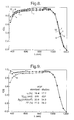
- Fig. 8 shows IQE measurements on wafers of different thicknesses that have otherwise equally been processed.
- IQE is enhanced for wavelengths below about 950 nm due to an increased LD/w ratio, which increases charge carrier collection. All photons corresponding to wavelengths below 850 nm are absorbed in a 150 ⁇ m thick wafer. Therefore the greater LD/w is the more effective is the charge carrier collection on the rear side. For wavelengths greater than 1000 nm, the absorption of photons is reduced with decreased w, resulting in a reduced IQE for thinner wafers in the long wavelength regime.
- V OC has a flat maximum at 200 ⁇ m (630 mV) and is also nearly the same within process accuracy for 150 ⁇ m thick cells (627 mV), but definitely is increased compared to solar cells with 250 ⁇ m (621 mV). Therefore, the actual FSF and surface passivation seems to be good enough for wafer thicknesses of about 200 ⁇ m. With reduced wafer thickness, the FSF and surface passivation are more important due to a reduced importance of recombination within the bulk of the solar cell. For the actual FSF it is assumed, that the optimum wafer thickness is about 200 ⁇ m.
- the FSF including the surface passivation can be optimised.
- the results of this optimisation will now be discussed, starting with the Front Surface Field.
- IQE is somewhat reduced in the blue wavelength regime due phosphorous diffusion on the front side of the wafer, resulting in an increased recombination in this highly doped layer.
- the reduction of the doping in the FSF would reduce recombination therein. Most favourable from this point of view would be even no extra front diffusion.
- Figure 9 shows cell performance for an n+ layer of standard doping in curve a) (50 Ohm/sq), and a shallow n+ layer of 80 Ohm/sq in curve b).
- the term shallow is used to refer to doping of relatively low concentration and/or a doping that is not very deep, and the combined effect can suitably be characterised by a sheet resistance.
- Shallow doping is referred to as doping of that results in a sheet resistance of 80 Ohm/sq and above.
- the shallow front surface diffusion results in a solar cell with further increased blue response, as shown in Figure 9. Not only the absorption in the blue wavelength regime is increased, but also the IQE is increased up to 900 nm. Again, especially for a rear junction solar cell, the effect of reducing the front surface recombination is much more important than for a front junction solar cell. With reduced front surface doping, the efficiency further increased to above 17%.
- Table IV shows a comparison of the standard p-type with the shallow rear junction emitter cell, and the difference between the two. For comparison the data for the standard rear junction emitter cell are also given. Table IV standard p-type cell rear junction n-type cell with shallow FSF diff. (%) rear junction n-type cell with standard FSF ⁇ (%) 17.2 17.2 0 16.4 J SC (mA/cm 2 ) 35.5 34.9 - 1.7 33.9 V OC (mV) 619 632 + 2.1 629 FF (%) 78.3 78.0 - 0.4 77.5
- the reduced J SC is likely due to the rear junction concept, where a not perfect surface passivation as well as a finite LD/w ratio can limit the efficiency more drastically than in a front junction solar cell concept. Anyhow, this is compensated by higher v OC , and it is clearly shown, that the rear junction concept on n-type silicon can lead to similar efficiencies as standard Shell Solar p-type front junction solar cells.
- SiN(No.1) a cell with shallow n+ layer on the front side and a SiN passivation layer that was applied by a so-called LP (low pressure) process, hereafter referred to as SiN(No.1); a cell without shallow n+ layer and SiN passivation layer applied via PE-CVD [SiN(No.2); and a cell with shallow n+ layer and a PE-CVD generated SiN layer [SiN(No.3)].
- SiN(No.1) a cell with shallow n+ layer on the front side and a SiN passivation layer that was applied by a so-called LP (low pressure) process
- SiN(No.2) a cell without shallow n+ layer and SiN passivation layer applied via PE-CVD
- SiN(No.3) a cell with shallow n+ layer and a PE-CVD generated SiN layer
- Fig. 10 shows the effective lifetime t eff (excess charge carrier density 10 15 .cm -3 ) measured on textured, n-type wafers provided on both sides with a phosphorous diffused doping layer and SiN coating, that have had the same process steps, as the n-type shallow rear junction solar cell discussed above, except for the boron diffusion.
- the samples have been pulled through a firing furnace that is usually used for contact formation of screen-printed solar cells.
- the n-type wafers are the same for all types of SiN depositions, it is assumed that the differences in effective lifetime reflects the surface passivation in a qualitative way.
- the life times, although not very high are, within the measurement accuracy, the same before and after firing. Apparently the surface passivation is not impacted during firing.
- Fig. 12 shows the result of this type of solar cell, processed on large area (148 cm 2 ), fully screen-printed.
- V OC of 636 mV indicates a good surface passivation.
- the cells still show a somewhat low J SC (35.1 mA/cm 2 ).
- the fill factor was 78.0%, and an efficiency of 17.4% was measured.
- n-type bare wafers do not show a measurable degradation. However, that does not exclude that there are other degradation mechanisms. It is known that the front surface of a n-type PERT cell strongly suffers from degradation with losses in V OC up to 100 mV. It is concluded that the boron diffused front side in combination with its non-stable surface passivation is responsible for the LID effect in these n-type silicon solar cells. Therefore in the following section LID is investigated for n-type solar cells with rear junction geometry.
- Fig. 13 shows the light induced degradation behaviour of rear junction the n-type silicon solar cell according to the invention, with SiN, and for comparison LID of a p-type silicon solar cell also processed at Shell Solar is shown. Both cells have a efficiency ⁇ of at least 17.2%.
- the p-type cell shows the behaviour as expected. The efficiency degrades up to 3% and saturates after about 24h. Heating the sample in ambient atmosphere for about 20 min at 200 °C completely recovers the efficiency to its initial value.
- the n-type cell with SiN (No. 3) passivation scheme degrades less than one percent, even after 100 h of illumination. Heating the sample after 100h of illumination reduces the LID effect to below 0.3% of its initial value. This is within the measurement accuracy of the measurement system, and is a very good indication for good long term stability.
- the invention has proven the successful development of a large area (125 x 125 cm 2 ) fully screen printed silicon solar cell on n-type wafers.
- the various optimisation steps allowed a final results that delivers n-type rear junction shallow front surface field SiN passivated solar cells with efficiencies in a narrow distribution around 17.4% (V OC : 636.2 mV, J SC : 35.1 mA/cm 2 , FF: 78.0%).
- the efficiency is at the same level as existing p-type Si technology, and generally significantly better than the best results for Cz wafer based cells using Al alloyed rear contacts reported before.
- the efficiency degradation of the new solar cells has been shown to be clearly below 1% after 100 h illumination.
- the new cells can be manufactured on commercial scale using in principle the same process steps as they are already in use for commercial production of p-type solar cells at Shell Solar GmbH.
Landscapes
- Engineering & Computer Science (AREA)
- General Physics & Mathematics (AREA)
- Microelectronics & Electronic Packaging (AREA)
- Power Engineering (AREA)
- Computer Hardware Design (AREA)
- Life Sciences & Earth Sciences (AREA)
- Physics & Mathematics (AREA)
- Condensed Matter Physics & Semiconductors (AREA)
- Electromagnetism (AREA)
- Sustainable Development (AREA)
- Crystallography & Structural Chemistry (AREA)
- Chemical & Material Sciences (AREA)
- Sustainable Energy (AREA)
- Manufacturing & Machinery (AREA)
- Photovoltaic Devices (AREA)
Priority Applications (2)
| Application Number | Priority Date | Filing Date | Title |
|---|---|---|---|
| EP05105081A EP1732142A1 (de) | 2005-06-09 | 2005-06-09 | Si Solarzelle und ihr Herstellungsverfahren |
| PCT/EP2006/062953 WO2006131526A1 (en) | 2005-06-09 | 2006-06-07 | Si solar cell and its manufacturing method |
Applications Claiming Priority (1)
| Application Number | Priority Date | Filing Date | Title |
|---|---|---|---|
| EP05105081A EP1732142A1 (de) | 2005-06-09 | 2005-06-09 | Si Solarzelle und ihr Herstellungsverfahren |
Publications (1)
| Publication Number | Publication Date |
|---|---|
| EP1732142A1 true EP1732142A1 (de) | 2006-12-13 |
Family
ID=34940138
Family Applications (1)
| Application Number | Title | Priority Date | Filing Date |
|---|---|---|---|
| EP05105081A Withdrawn EP1732142A1 (de) | 2005-06-09 | 2005-06-09 | Si Solarzelle und ihr Herstellungsverfahren |
Country Status (2)
| Country | Link |
|---|---|
| EP (1) | EP1732142A1 (de) |
| WO (1) | WO2006131526A1 (de) |
Cited By (7)
| Publication number | Priority date | Publication date | Assignee | Title |
|---|---|---|---|---|
| WO2010049268A1 (de) | 2008-10-31 | 2010-05-06 | Bosch Solar Energy Ag | Solarzelle und verfahren zu deren herstellung |
| WO2011029640A2 (en) | 2009-09-10 | 2011-03-17 | Q-Cells Se | Solar cell |
| JP2012124193A (ja) * | 2010-12-06 | 2012-06-28 | Sharp Corp | 裏面電極型太陽電池の製造方法、および裏面電極型太陽電池 |
| WO2012027000A3 (en) * | 2010-08-25 | 2012-08-30 | Suniva, Inc. | Back junction solar cell with selective front surface field |
| US20130056069A1 (en) * | 2007-02-16 | 2013-03-07 | Nanogram Corporation | Solar cell structures, photovoltaic panels and corresponding processes |
| EP3021365A1 (de) * | 2014-11-14 | 2016-05-18 | Commissariat à l'Energie Atomique et aux Energies Alternatives | Verfahren zur restaurierung von fotovoltaik-solarzellen auf siliziumbasis |
| CN111009592A (zh) * | 2019-11-04 | 2020-04-14 | 江苏杰太光电技术有限公司 | 一种SiO2及掺杂多晶硅叠层钝化薄膜的制备方法 |
Citations (4)
| Publication number | Priority date | Publication date | Assignee | Title |
|---|---|---|---|---|
| FR2505556A1 (fr) * | 1981-05-11 | 1982-11-12 | Labo Electronique Physique | Procede de fabrication de cellules solaires en silicium et cellules solaires ainsi obtenues |
| US4667060A (en) * | 1985-05-28 | 1987-05-19 | Spire Corporation | Back junction photovoltaic solar cell |
| WO1997013280A1 (en) * | 1995-10-05 | 1997-04-10 | Ebara Solar, Inc. | Self-aligned locally deep- diffused emitter solar cell |
| US6262359B1 (en) * | 1999-03-17 | 2001-07-17 | Ebara Solar, Inc. | Aluminum alloy back junction solar cell and a process for fabrication thereof |
-
2005
- 2005-06-09 EP EP05105081A patent/EP1732142A1/de not_active Withdrawn
-
2006
- 2006-06-07 WO PCT/EP2006/062953 patent/WO2006131526A1/en active Application Filing
Patent Citations (4)
| Publication number | Priority date | Publication date | Assignee | Title |
|---|---|---|---|---|
| FR2505556A1 (fr) * | 1981-05-11 | 1982-11-12 | Labo Electronique Physique | Procede de fabrication de cellules solaires en silicium et cellules solaires ainsi obtenues |
| US4667060A (en) * | 1985-05-28 | 1987-05-19 | Spire Corporation | Back junction photovoltaic solar cell |
| WO1997013280A1 (en) * | 1995-10-05 | 1997-04-10 | Ebara Solar, Inc. | Self-aligned locally deep- diffused emitter solar cell |
| US6262359B1 (en) * | 1999-03-17 | 2001-07-17 | Ebara Solar, Inc. | Aluminum alloy back junction solar cell and a process for fabrication thereof |
Non-Patent Citations (1)
| Title |
|---|
| SALAMI J ET AL: "Self-aligned locally diffused emitter (SALDE) silicon solar cell", SOLAR ENERGY MATERIALS AND SOLAR CELLS, ELSEVIER SCIENCE PUBLISHERS, AMSTERDAM, NL, vol. 48, no. 1-4, November 1997 (1997-11-01), pages 159 - 165, XP004111846, ISSN: 0927-0248 * |
Cited By (18)
| Publication number | Priority date | Publication date | Assignee | Title |
|---|---|---|---|---|
| US9343606B2 (en) * | 2007-02-16 | 2016-05-17 | Nanogram Corporation | Solar cell structures, photovoltaic panels and corresponding processes |
| US20130056069A1 (en) * | 2007-02-16 | 2013-03-07 | Nanogram Corporation | Solar cell structures, photovoltaic panels and corresponding processes |
| WO2010049268A1 (de) | 2008-10-31 | 2010-05-06 | Bosch Solar Energy Ag | Solarzelle und verfahren zu deren herstellung |
| CN102203959B (zh) * | 2008-10-31 | 2014-03-26 | 罗伯特·博世有限公司 | 太阳能电池及其制造方法 |
| CN102203959A (zh) * | 2008-10-31 | 2011-09-28 | 罗伯特·博世有限公司 | 太阳能电池及其制造方法 |
| DE102009043975B4 (de) * | 2009-09-10 | 2012-09-13 | Q-Cells Se | Solarzelle |
| CN102484146A (zh) * | 2009-09-10 | 2012-05-30 | Q-电池公司 | 太阳能电池 |
| WO2011029640A3 (en) * | 2009-09-10 | 2012-02-09 | Q-Cells Se | Solar cell |
| DE102009043975A1 (de) | 2009-09-10 | 2011-03-24 | Q-Cells Se | Solarzelle |
| CN102484146B (zh) * | 2009-09-10 | 2014-11-19 | Q-电池公司 | 太阳能电池 |
| WO2011029640A2 (en) | 2009-09-10 | 2011-03-17 | Q-Cells Se | Solar cell |
| WO2012027000A3 (en) * | 2010-08-25 | 2012-08-30 | Suniva, Inc. | Back junction solar cell with selective front surface field |
| JP2013536589A (ja) * | 2010-08-25 | 2013-09-19 | サニーバ,インコーポレイテッド | 選択的表面電界を有する裏面接合型太陽電池 |
| KR101436357B1 (ko) * | 2010-08-25 | 2014-09-02 | 수니바 인코포레이티드 | 선택적 전면 필드를 구비한 후면 접합 태양전지 |
| JP2012124193A (ja) * | 2010-12-06 | 2012-06-28 | Sharp Corp | 裏面電極型太陽電池の製造方法、および裏面電極型太陽電池 |
| EP3021365A1 (de) * | 2014-11-14 | 2016-05-18 | Commissariat à l'Energie Atomique et aux Energies Alternatives | Verfahren zur restaurierung von fotovoltaik-solarzellen auf siliziumbasis |
| FR3028669A1 (fr) * | 2014-11-14 | 2016-05-20 | Commissariat Energie Atomique | Procede de restauration de cellules solaires photovoltaiques a base de silicium |
| CN111009592A (zh) * | 2019-11-04 | 2020-04-14 | 江苏杰太光电技术有限公司 | 一种SiO2及掺杂多晶硅叠层钝化薄膜的制备方法 |
Also Published As
| Publication number | Publication date |
|---|---|
| WO2006131526A1 (en) | 2006-12-14 |
Similar Documents
| Publication | Publication Date | Title |
|---|---|---|
| US8349644B2 (en) | Mono-silicon solar cells | |
| KR101436357B1 (ko) | 선택적 전면 필드를 구비한 후면 접합 태양전지 | |
| EP2165371B1 (de) | Verfahren zur herstellung einer emitterstruktur und daraus resultierende emitterstrukturen | |
| US9634160B2 (en) | Solar cell and method for manufacturing the same | |
| US20060130891A1 (en) | Back-contact photovoltaic cells | |
| US20110114171A1 (en) | Solar cell including sputtered reflective layer | |
| US20070295399A1 (en) | Back-Contact Photovoltaic Cells | |
| US20070137692A1 (en) | Back-Contact Photovoltaic Cells | |
| KR20100015622A (ko) | 태양 전지 | |
| US9978888B2 (en) | Solar cell and method for manufacturing the same | |
| WO2010104726A2 (en) | Heterojunction solar cell based on epitaxial crystalline-silicon thin film on metallurgical silicon substrate design | |
| US20100276772A1 (en) | Photoelectric conversion device and method of manufacturing photoelectric conversion device | |
| EP1732142A1 (de) | Si Solarzelle und ihr Herstellungsverfahren | |
| EP2296192A1 (de) | Solarzelle und herstellungsverfahren dafür | |
| Haverkamp et al. | Minimizing the electrical losses on the front side: development of a selective emitter process from a single diffusion | |
| US9997647B2 (en) | Solar cells and manufacturing method thereof | |
| US20130247981A1 (en) | Solar cell fabrication using a pre-doping dielectric layer | |
| EP3163632A1 (de) | Fotovoltaisches modul und verfahren zur herstellung davon | |
| WO2012129184A1 (en) | Insitu epitaxial deposition of front and back junctions in single crystal silicon solar cells | |
| KR20100089473A (ko) | 고효율 후면 전극형 태양전지 및 그 제조방법 | |
| Raabe et al. | The development of etch-back processes for industrial silicon solar cells | |
| JP5645734B2 (ja) | 太陽電池素子 | |
| WO2014171686A1 (en) | Solar cell and manufacturing method thereof | |
| KR101431266B1 (ko) | 태양전지의 제조방법 | |
| Schmich et al. | Emitter epitaxy for crystalline silicon thin film solar cells with new contact methods |
Legal Events
| Date | Code | Title | Description |
|---|---|---|---|
| PUAI | Public reference made under article 153(3) epc to a published international application that has entered the european phase |
Free format text: ORIGINAL CODE: 0009012 |
|
| AK | Designated contracting states |
Kind code of ref document: A1 Designated state(s): AT BE BG CH CY CZ DE DK EE ES FI FR GB GR HU IE IS IT LI LT LU MC NL PL PT RO SE SI SK TR |
|
| AX | Request for extension of the european patent |
Extension state: AL BA HR LV MK YU |
|
| 17P | Request for examination filed |
Effective date: 20070105 |
|
| 17Q | First examination report despatched |
Effective date: 20070214 |
|
| AKX | Designation fees paid |
Designated state(s): AT BE BG CH CY CZ DE DK EE ES FI FR GB GR HU IE IS IT LI LT LU MC NL PL PT RO SE SI SK TR |
|
| STAA | Information on the status of an ep patent application or granted ep patent |
Free format text: STATUS: THE APPLICATION IS DEEMED TO BE WITHDRAWN |
|
| 18D | Application deemed to be withdrawn |
Effective date: 20070626 |