EP1732080A1 - Method for extracting the distribution of charge stored in a semiconductor device - Google Patents
Method for extracting the distribution of charge stored in a semiconductor device Download PDFInfo
- Publication number
- EP1732080A1 EP1732080A1 EP05109600A EP05109600A EP1732080A1 EP 1732080 A1 EP1732080 A1 EP 1732080A1 EP 05109600 A EP05109600 A EP 05109600A EP 05109600 A EP05109600 A EP 05109600A EP 1732080 A1 EP1732080 A1 EP 1732080A1
- Authority
- EP
- European Patent Office
- Prior art keywords
- charge
- pumping
- cyc
- distribution
- channel
- Prior art date
- Legal status (The legal status is an assumption and is not a legal conclusion. Google has not performed a legal analysis and makes no representation as to the accuracy of the status listed.)
- Granted
Links
Images







Classifications
-
- G—PHYSICS
- G11—INFORMATION STORAGE
- G11C—STATIC STORES
- G11C16/00—Erasable programmable read-only memories
- G11C16/02—Erasable programmable read-only memories electrically programmable
- G11C16/04—Erasable programmable read-only memories electrically programmable using variable threshold transistors, e.g. FAMOS
- G11C16/0466—Erasable programmable read-only memories electrically programmable using variable threshold transistors, e.g. FAMOS comprising cells with charge storage in an insulating layer, e.g. metal-nitride-oxide-silicon [MNOS], silicon-oxide-nitride-oxide-silicon [SONOS]
- G11C16/0475—Erasable programmable read-only memories electrically programmable using variable threshold transistors, e.g. FAMOS comprising cells with charge storage in an insulating layer, e.g. metal-nitride-oxide-silicon [MNOS], silicon-oxide-nitride-oxide-silicon [SONOS] comprising two or more independent storage sites which store independent data
-
- G—PHYSICS
- G11—INFORMATION STORAGE
- G11C—STATIC STORES
- G11C16/00—Erasable programmable read-only memories
- G11C16/02—Erasable programmable read-only memories electrically programmable
- G11C16/06—Auxiliary circuits, e.g. for writing into memory
- G11C16/26—Sensing or reading circuits; Data output circuits
-
- G—PHYSICS
- G11—INFORMATION STORAGE
- G11C—STATIC STORES
- G11C16/00—Erasable programmable read-only memories
- G11C16/02—Erasable programmable read-only memories electrically programmable
- G11C16/06—Auxiliary circuits, e.g. for writing into memory
- G11C16/34—Determination of programming status, e.g. threshold voltage, overprogramming or underprogramming, retention
- G11C16/349—Arrangements for evaluating degradation, retention or wearout, e.g. by counting erase cycles
- G11C16/3495—Circuits or methods to detect or delay wearout of nonvolatile EPROM or EEPROM memory devices, e.g. by counting numbers of erase or reprogram cycles, by using multiple memory areas serially or cyclically
Definitions
- the present invention is in the field of semiconductor processing and devices, more specifically in the field of non-volatile charge-trapping memory devices.
- the present invention relates to a method for extracting the spatial distribution of charge stored in a charge-trapping layer of a semiconductor device, according to the preamble of the first claim.
- Non-volatile memories are characterized by the fact that once a bit is stored in a memory cell this bit will be retained even when the memory cell is no longer powered.
- the NVM devices are also known as EEPROM (Electrically-Erasable-and-Programmable-Read-Only-Memory) devices.
- EEPROM Electrically-Erasable-and-Programmable-Read-Only-Memory
- charge-trapping EEPROM devices charge is stored in a non-conductive layer being part of a single-capacitor structure. In such non-conductive charge-storage layer, e.g.
- charge-trapping memory devices are characterized by the presence of discrete charge traps as memory elements contrary to floating gate memory devices where a conductive layer is used as one continuous charge trap for storing charge. Developments in EEPROM devices are increasingly focused on localized charge trapping because it eases integration and reduces stress-induced-leakage.
- NROMTM devices using nitride as non-conductive charge-storage layer as disclosed for example by B.
- Eitan in international application W099/070000 are very attractive since they allow storage of two physical bits per memory cell, each bit at a different location in the nitride charge-storage layer.
- carriers e.g. electrons
- the NROMTM cell is programmed.
- opposite-type carriers are injected in the nitride layer as to compensate the charge stored during programming, e.g. holes are injected in the nitride layer to compensate the electrons already present.
- poor endurance and poor retention after cycling i.e. repetitive programming and erasing of a cell, are major drawbacks of NROMTM.
- Rosmeulen et al teaches in "Characterization of the spatial charge distribution in local charge-trapping memory devices using the charge-pumping technique", (Solid-State Electronics journal, volume 48 (2004) p1525-1530 ), the application of the charge-pumping technique to non-volatile memory devices which are based on localized trapping of charge, in particular to n-type NROM TM devices using nitride or silicon-rich-oxide as trapping medium and injection of electrons for programming the memory cell.
- section 3.3 of this disclosure hereby incorporated by reference in its entirety, teaches how the lateral distribution of the total charge trapped in the device can be directly calculated from the charge-pumping measurements using a deconvolution-based procedure.
- this measurement procedure allows extracting the lateral distribution of electrons injected in the device during a programming step, it doesn't take into account the variation of the density of charge traps present at the interface between the channel and the dielectric stack and assumes this density to be uniform along the channel. Moreover when the device is subjected to multiple program/erase steps, this interface will be degraded due to this electrical stress. Additional interface traps N it will be formed in a non-uniform way, in particular when erasing the memory device by injection of holes.
- An aim of the invention is to disclose a method for determining the charge distribution in a non-volatile charge-trapping memory device. This aim is achieved with the method comprising the steps of claim 1.
- the method of the invention is developed for extracting the spatial distribution of charge stored in a charge-trapping layer of a semiconductor device, which has a channel underneath the charge trapping layer with a given effective length L eff .
- the method comprises the following steps. Two charge pumping curves are determined, one by using a varying base-level voltage measurement and the other by using a varying top-level voltage measurement in the charge-pumping technique. More particularly, the first curve is determined by a first charge-pumping measurement on the semiconductor device whereby only the upper level of the charge-pump pulse is varied and the second curve is determined by a second charge-pumping measurement on the semiconductor device whereby only the lower level of the charge-pump pulse is varied. The data from the first and second charge-pumping measurements is combined to obtain the spatial distribution of the charge in the charge-trapping layer.
- a relation is established between a charge pumping current I cp and a calculated channel length L calc of the semiconductor device by reconstructing a spatial charge distribution from the charge pumping curves for multiple values of the charge pumping current I cp . These values are preferably chosen in the upper range of the charge pumping curves, more preferably as close as possible to where one assumes the maximum charge pumping current I cp_max to be, but this is not essential. From the multiple values of I cp , that value is selected for which the corresponding calculated channel length L calc is substantially equal to the effective channel length L eff of the semiconductor device. Finally, the spatial charge distribution is reconstructed from the charge pumping curves using this value of I cp .
- the extraction method of the invention allows extracting the distribution of the electrons and holes injected into the charge-trapping layer of the memory device and hence to determine the voltage settings required to obtain the selected charge distribution.
- the combining of data from the charge pumping curves comprises the following steps. First, one value as charge pumping current I cp is selected on one of the charge pumping profiles. Next, the calculated channel length L calc corresponding to the selected charge pumping current I cp is determined by reconstructing the spatial charge distribution for this charge pumping current I cp . Then, the calculated channel length L calc is compared with the effective length L eff . In case of a mismatch, a new value for the charge pumping current I cp is determined, using the mismatch as information to improve the choice. These steps are repeated until the mismatch substantially becomes zero.
- the data from the charge pumping curves is further combined to obtain a spatial distribution of charge in traps present at the interface between the channel and a dielectric stack which separates the charge trapping layer from the channel.
- This embodiment is a method to separately extract the spatial distribution of the charge stored in the charge-trapping layer of a charge-trapping device and of the charge stored in the interface traps. If these two charge distributions are known one can also characterise the injection of holes into this charge-trapping layer, even if a non-uniform distribution of interface traps is created by injection of holes. This method thus also allows separately extracting hole and electron profiles within a charge-trapping layer of a charge-trapping device.
- FIG. 1 shows a schematic cross-section of a MOSFET-type device.
- This device (1) comprises a gate electrode (3) separated from the substrate (2) by a gate dielectric (4).
- the gate electrode is formed from a semiconductor material such as polycrystalline silicon doped to obtain the desired workfunction and/or conductivity.
- This semiconductor material can be partially or fully silicided as known in the art or even metals, e.g. Al, TiN, TaN, are used.
- the gate dielectric (8) comprises a dielectric charge-trapping layer (10) such as silicon-nitride, silicon-rich oxide, silicon-oxynitride, an oxide layer comprising nanocrystals of a semiconductor material, e.g. polycrystalline silicon.
- this charge-trapping layer can be separated from the substrate (2) by another dielectric layer (11) with low or no trapping capabilities, e.g. silicon-oxide.
- Another layer (9) in a similar material as layer (11) can be used to separate the charge-trapping layer (10) from the gate electrode (3).
- the substrate (2) is a semiconductor substrate, e.g. silicon, silicon-on-insulator (SOI), germanium-on-insulator (GOI).
- SOI silicon-on-insulator
- GOI germanium-on-insulator
- sidewall spacers (5) formed in a dielectric material such as silicon-oxide, silicon-oxynitride, silicon-carbide can be present. Aligned to this stack source (6) and drain regions (7) are formed in the substrate (2).
- the source (6) and drain regions (7) are of an opposite conductivity type as the substrate (2).
- the source (6) and drain regions (7) extend under the spacers (5) such that the channel region (8) is contacted.
- This channel region (8) is under dielectric control of the gate electrode (3).
- the device of figure 1 can be manufactured using processing steps and materials known to any person skilled in the art of manufacturing semiconductor devices, in particular non-volatile memory devices.
- the device (1) is a nMOS device comprising a polysilicon gate electrode (3), which is n-type doped. Also source (6) and drain (7) regions are n-type doped while the substrate (2) is p-type doped. Sidewall spacers (5) formed in silicon-oxide are present.
- the gate dielectric (4) consists of a nitride layer used as charge-trapping layer (10) sandwiched between two layers (9, 11) of silicon-oxide.
- the device can be a pMOS device comprising device comprising a polysilicon gate electrode (3), which is p-type doped.
- source (6) and drain (7) regions are p-type doped while the substrate (2) is n-type doped.
- the device can be a split gate device such as the HIMOS memory cell disclosed in US5,583,811 hereby incorporated by reference in its entirety Accordingly, the description should not be deemed to be limiting in scope.
- all methods for extracting the spatial distribution of charge N nt stored in the charge-trapping layer (10) of the semiconductor device (1) comprise the following steps: determining a varying base-level voltage V base charge pumping curve, determining a varying top-level voltage V top charge pumping curve, and combining data from the charge pumping curves to obtain the spatial distribution of the stored charge N nt .
- This combination of data is done by establishing a relation between a charge pumping current I cp and a calculated channel length L calc of the semiconductor device by reconstructing a spatial charge distribution from the charge pumping curves for multiple values of the charge pumping current I cp .
- this charge-trapping device is a non-volatile charge-trapping memory device.
- a charge-pumping measurement set-up which can be used in for determining the charge pumping curves, is schematically shown in figure 1a.
- Source (6), drain (7) and substrate (2) regions are biased to a fixed voltage, preferably 0V or ground.
- a voltage source e.g. a pulse generator, is connected to the gate electrode while current is measured at the substrate.
- This measurement set-up is also known as amplitude-sweep charge-pumping set-up as the amplitude of the voltage pulses applied to the gate electrode is increased during the measurement.
- the measurement sequence comprises two steps: first two charge-pumping measurements are performed on a device used as reference and secondly similar charge-pumping measurements are performed on the device-under-test (DUT).
- the reference device is usually the same as the studied device but in a reference state.
- the studied device needs to have a monotonic increase or decrease of the threshold voltage along the channel, or at least along the part of the channel, which is subjected to the measurement method, typically half of the channel.
- each threshold voltage value corresponds to one point of the charge-pumping curve.
- the reference state of this device more precisely the threshold voltage distribution thereof depends on the charge already trapped in the studied device. If the threshold voltage distribution in the studied device increases monotonically, it is better to have the reference state having a similar increase in threshold voltage distribution.
- the pristine device can be subjected to a light programming operation resulting in a monotonic increase of the charge in the charge-trapping layer which results in a threshold profile V th (x) that monotonic varies along the channel as shown in figure 2 by the dotted line V th_ref (x).
- V th (x) a threshold profile
- V th_ref (x) a threshold profile
- the threshold voltage of the device in the reference state slightly increase near the drain d.
- the number and distribution of the interface traps should remain essentially unaffected and essentially uniform over the channel. If the threshold voltage distribution monotonically decreases, it is better to have the reference state with also a decreasing threshold voltage distribution.
- the most natural reference state is in this case the virgin device, where the threshold voltage progressively decreases from the center of the channel to the junction.
- a first charge-pumping measurement is performed on the device in the reference state that has not yet been electrically stressed, i.e. the interface trap distribution can be considered uniform along the channel.
- a first pulse train is applied to the gate electrode (3), whereby each pulse in this pulse train has the same bottom-level V bot .
- the amplitude V p of the pulses increases monotonically with time by increasing the top-level V top of the pulses.
- the exemplary pulse train shown in figure 1 b comprises 9 pulses grouped in sets of 3. The pulses in the first set have the lowest amplitude, the pulses in the second set have a higher amplitude, while the pulses in the last set have the highest amplitude.
- the amplitude of the pulse in the pulse sequence or the voltage swing of each pulse increases progressively.
- the number of pulses in the pulse train, their duty cycle, the amplitude of each pulse, the way the amplitude V p is increased over the pulse train, e.g. stepwise, gradually, and the upper level V top are parameters of choice and can be selected in view of the required accuracy and measurement resolution.
- the charge-pump current is proportional to the pulse frequency and the number of interface states N it in the inversion region formed in the channel. From this charge-pumping measurement the charge-pump curve I cp (V P ) of this device in the reference state is obtained as shown in figure 1c given the current I cp or charge per pulse as function of the top level V top of the pulse train.
- I cp V P
- a second charge-pumping measurement is performed on the device in the reference state.
- a pulse train is applied to the gate electrode (3), whereby each pulse in this pulse train has the same top-level V top .
- the amplitude V p of the pulses increases monotonically with time by lowering the bottom-level V bot of the pulses.
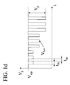
- the exemplary pulse train shown in figure 1d comprises 9 pulses grouped in sets of 3. The pulses in the first set have the lowest amplitude or voltage swing, the pulses in the second set have a higher amplitude, while the pulses in the last set have the highest amplitude.
- stepwise, gradually, the upper level V top are parameters of choice and can be selected in view of the required accuracy and measurement resolution.
- This pulse train with fixed top-level V top and varying bottom-level V bot will fill the interface states with electrons during the uptime t up of the pulse and with holes during the downtime t do of the pulse when V bot is below the flatband voltage V fb_H .
- the channel will remain in inversion and the interface traps are always filled with electrons.
- the channel (8) will switch between inversion and accumulation depending on whether the lower level V bot of the progressively increased pulse amplitude is above or below this flatband voltage V fb-H and the interface traps will be alternatively filled with electrons and holes during the charge-pumping measurements.
- the charge-pump curve I cp (V P ) of this device in the reference state is obtained as shown in figure 1 e given the current I cp or charge per pulse as function of the bottom level V bot of the pulse train.
- the maximum I cp_max current corresponds to one end of the channel, e.g.
- a device under test is electrically stressed resulting in charged carriers to be injected into the charge-trapping layer (10). These injected carriers can be positively or negatively charged.
- one carrier type is used to program the memory cell while the opposite charged carriers are used to erase the memory cell by compensating the distribution profile of the programmed charge.
- charge-pumping measurements according to the present invention are performed to determine the contribution to the threshold voltage of the charge Q nt stored in the charge-trapping layer (10) and the charge Q it generated by the interface traps N it .
- the charge Q nt stored in the charge-trapping layer (10) generates a constant offset of the threshold voltage ⁇ V th_Qnt , while the offset ⁇ V th_Qit generated by the charge stored in the interface traps depends on whether positive or negative charge is stored in these interface traps and on the number of interface traps N it .
- the interface traps are filled with electrons causing an upward shift of the threshold voltage, while in accumulation the interface traps are filled with holes causing a downward shift of the threshold voltage.
- the degradation of a device e.g. by repetitive electrical stress applied to the device, will change the number of interface traps and hence the threshold voltage offset ⁇ V th_Qit .
- a threshold voltage distribution shown in figure 2 can result from negative charge e.g.
- the charge-trapping layer (10) of an nMOS device present in the charge-trapping layer (10) of an nMOS device.
- a similar figure can be drawn for the flatband voltage distribution of this device.
- electrons can be injected into this layer (10) during the step of programming the memory cell, e.g. by channel-hot-electron-injection as is known in the art.
- Holes can be injected during the step of erasing the memory cell, e.g. by band-to-band tunneling induced hot hole injection as is known in the art. This localized trapped charge, e.g.
- FIG. 3a illustrates such a device wherein a number N nt of negative charged particles (dotted area between position x 1 and drain d) is stored in the charge-trapping layer (10) resulting in an increase of the threshold voltage and flatband voltage in the portion x 1 to d compared to the portion s to x 1 .
- a pulse train similar to the pulse train of the first measurement on the device in the reference state and illustrated by figure 3b is applied to this device also.
- this pulse train with fixed bottom-level V bot and varying top-level V top will fill the interface states with electrons during the uptime t up of the pulse and with holes during the downtime t do of the pulse in these locations where the pulse is swept over the corresponding threshold voltage. If the number of interface states or the threshold voltage were uniform over the channel (8), one would obtain the same charge-pump current at each pulse independently of the amplitude of the pulse as long as V top is higher than the threshold voltage V th . If however the threshold voltage is not constant over the channel, as shown in figure 2, with increasing pulse amplitude V p an increasing portion of the channel will contribute to the charge pump current.
- the portion of the channel between x 1 and d will not contribute to the charge-pumping current.
- the portion of channel (8) having the higher threshold voltage V th_H will remain in accumulation and the corresponding interface traps will be always filled with holes as shown in figure 3a by the symbol h + .
- the portion of the channel (8) having the lower threshold voltage V th_L will switch between inversion and accumulation depending on whether the upper level V top is above or below this lower threshold voltage and the corresponding interface traps will be alternatively filled with electrons and holes during the charge-pumping measurement.
- the channel is scanned from source to drain if the threshold voltage V th (x) increases monotonically from the source to the drain. If only half of the channel is degraded, V th (x) needs to be monotonic only on half of the channel.
- the same procedure as applied to the charge-pumping signal in the first step for extracting the threshold voltage profile V th (x) from the charge-pumping current for the device under test is applied to this stressed device as illustrated by figure 3c.
- a relationship between the threshold voltage profile V th (x) and the location x in the channel can be established by the fact that the increase of the charge-pump current I cp from one location x 1 in the channel to another location x 2 can be attributed to the number of interface traps N it present in the channel area between these location.
- This relationship is expressed as follows: ⁇ X 1 X 2 q f N i t x d x ⁇ I c p V t h x 2 ⁇ I c p V t h x 1 with q the absolute value of the electron charge, f the frequency of the pulse.
- the dotted line indicates the reference charge-pump curve while the solid line indicates the charge-pumping curve obtained on the stressed device.
- the concentration of charge in the charge-storage layer N nt (x) (#/cm 2 ) is positive if electrons are trapped, while the local concentration of interface traps N it (x) is also in (#/cm 2 ).
- concentration of charge in the charge-storage layer N nt (x) (#/cm 2 ) is positive if electrons are trapped, while the local concentration of interface traps N it (x) is also in (#/cm 2 ).
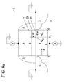
- FIG. 4a illustrates such a device wherein a number N nt of negative charged particles (dotted area between position x 1 and drain d) is stored in the charge-trapping layer (10). A number of interface states Nit is present (dots in the channel).
- a pulse train similar to the pulse train applied during the second measurement on the device in the reference state, is applied to the gate electrode (3), whereby each pulse in this pulse train has the same top-level V toP .
- the amplitude V p of the pulses increases monotonically with time by lowering the bottom-level V bot of the pulses.
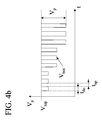
- the exemplary pulse train shown in figure 4b comprises 9 pulses grouped in sets of 3.
- the pulses in the first set have the lowest amplitude or voltage swing, the pulses in the second set have a higher amplitude, while the pulses in the last set have the highest amplitude.
- the number of pulses in the pulse train, their duty cycle, the amplitude of each pulse, the way the amplitude V p is increased over the pulse train, e.g. stepwise, gradually, the upper level V top are parameters of choice and can be selected in view of the required accuracy and measurement resolution.
- This pulse train with fixed top-level V top and varying bottom-level V bot will fill the interface states with electrons during the uptime t up of the pulse and with holes during the downtime t do of the pulse in these locations where the pulse is swept over the corresponding flatband voltage.
- the channel is scanned from drain to source if the flatband voltage V fb (x) increases monotonically from the source to the drain.
- the same procedure as applied to the charge-pumping signal in the first step for extracting the flatband voltage V fb (x) profile from the charge-pumping current for the device under test is applied to this stressed device as illustrated by figure 4c.
- a relationship between the flatband voltage profile V fb (x) and the location x in the channel can be established by the fact that the increase of the charge-pump current I cp from one location x 1 in the channel to another location x 2 can be attributed to the number of interface traps N it present in the channel area between these location.
- the concentration of charge in the charge-storage layer N nt (x) (#/cm 2 ) is positive if electrons are trapped, while the local concentration of interface traps N it (x) is also in (#/cm 2 ).
- the charge-pumping curves of figure 4c are obtained.
- the threshold voltage and flatband voltage at any given point is determined by the charge at that point: electrons stored in the charge-trapping layer (10) and the electrons trapped in the interface states.
- the charge-pumping curves obtained on the stressed device are compared with the charge-pumping curve of the reference device or unstressed device.
- the deviation between the reference curves on the one hand and the corresponding stressed curves is due to the overall threshold or flatband voltage variation caused by the charge in the charge-trapping layer (10) and in the interface states.
- the difference between the two deviations is due to the charge in the interface states only.
- I cp_max The correlation between the two measurements on the stressed device depend on I cp_max , which makes the results of the extraction very sensitive to this value.
- the charge-pumping curves saturate completely if the top level of the pulse is high enough (or if the base level of the pulse is low enough, following the type of measurement).
- the measurements in figure 6 show that the saturation is in reality not perfect, curves slightly continue to increase for high voltages. This causes incertitude on I cp_max .
- I cp_max The best choice of I cp_max is explained later in this text.
- Equation [1] can be written as: ⁇ X i ⁇ 1 X i q f N i t x d x ⁇ N i t x i ⁇ N i t x i ⁇ 1 x i ⁇ x i ⁇ 1 2 ⁇ I c p V th_cyc x i ⁇ I c p V th_cyc x i ⁇ 1
- Equation [6] By solving successively equations [6] and [7] from a starting point x o to a final point x end one can find the position x i from equation [7] which corresponds to the interface states N it (x i ) from equation [6].
- the profile of charge in the charge-trapping layer can be found by either solving equation [2] or [4].
- equation [6] If the difference (V th_ref (x)-V fb_ref (x)) in equation [6] is constant, because the number of interface traps N it,ref of the device in the reference state is constant and equal to the ratio (I cp_max /L eff ), this difference is given by combining the threshold voltage profile and flatband voltage profile given by respectively figure 1c and 1e.
- equation [5] allows to determine for a selected threshold voltage V th_cyc the corresponding flatband voltage V fb_cyc , as the sum of the corresponding charge-pump currents must be equal to the maximum charge-pump current I cp_max .
- the two charge-pumping curves used in the extraction method of the previous embodiments are shown.
- the charge-pumping current I cp reaches a maximum charge-pumping current I cp_max corresponding to a voltage bias V top or V bot wherein the complete area of the channel (8) having a known channel length L eff contributes to the charge-pumping current.
- I cp_max a maximum charge-pumping current I cp_max corresponding to a voltage bias V top or V bot wherein the complete area of the channel (8) having a known channel length L eff contributes to the charge-pumping current.
- I cp_max one can reconstruct the spatial distribution of charge N nt stored in the charge-trapping layer (10) of a semiconductor device (1).
- the current measured when applying a varying base-level or top-level voltage pulse sequence might not reach a maximum value and will continue to vary with varying pulse voltage.
- the charge pumping curves are combined as follows. As described before, a relation between the charge pumping current I cp and the calculated channel length L calc of the semiconductor device is established. In this embodiment, this is done by selecting on one of the charge pumping curves at least two charge pumping currents I cp and determining the calculated channel length L calc corresponding to each of the charge pumping currents I cp by reconstructing the spatial charge distribution for each of the charge pumping currents I cp . In this way, a set of at least two datapoints (L calc , I cp ) is obtained. From this set of datapoints, the charge pumping current I cp having a channel length substantially equal to the effective length L eff i.e. the maximum charge pumping current I cp_max can be obtained as follows.
- L calc L eff
- known numerical analytical techniques such as linear interpolation or binary search to determine this datapoint (L eff , I cp_max ).
- the first values of the charge pump current I cp are selected from the upper current range of the measured charge-pumping curve as such selection will speed up the extraction process.
- the first values of the charge pump current I cp are selected from the upper current range of the measured charge-pumping curve as such selection will speed up the extraction process.
- the calculated channel length L calc is compared with the effective length L eff and in case of a mismatch, a new value for the charge pumping current I cp is determined using the information given by the mismatch, i.e. the selection of the value for the charge pumping current I cp is optimised.
- the determined charge pumping current I cp is said to correspond to the maximum charge pumping current I cp_max , when the difference between the obtained calculated channel length L calc and the effective length L eff is less than 2%, preferably less than 1% of the effective channel length L eff .
- extraction methods according to the present application are particular useful for extracting the spatial distribution of charge N nt stored in the charge-trapping layer (10) of a memory device (1)
- these extraction methods can be applied to any kind of semiconductor device (1) wherein a dielectric stack (4) is sandwiched between an electrode (3) and a semiconductor region (2).
- the disclosed extraction methods can be used to the extract charge stored in this dielectric stack (4).
- charge might be unintentionally incorporated in the gate dielectric (4).
- this incorporated charge might result from the device operation, e.g. hot carriers, or result from the semiconductor manufacturing process introducing fixed or mobile charge in the gate dielectric.
- This gate dielectric can be of a single dielectric material such as silicon-oxide, silicon-oxy-nitride, a high-k dielectric such as alumina-oxide, hafnium-oxide, hafnium-silicon-oxide as known in the art.
- this gate dielectric can be a stack of dielectric materials, e.g. a high-k dielectric formed upon a silicon-oxide.
- this charge N nt will also influence the threshold voltage profile V th (x) and flatband voltage profile V fb (x) of the logic transistor.
- the disclosed extraction methods can also be applied to such logic transistor to determine the spatial distribution of the incorporated charge N nt .
- the spatial charge distribution N nt is reconstructed from the charge pumping curves by combining data from these charge pumping curves to obtain the spatial distribution.
- This data from the charge pumping curves can be further combined to obtain a spatial distribution of charge (N it ) in traps present at the interface between the channel (8) and a dielectric stack (4).
- the present extraction methods also allow determining the spatial distribution of this interface charge N it , even when charge is present in the dielectric stack (4). The dependency of this interface charge on parameters of the semiconductor process or of device operation can thus more accurately be determined.
- FIGS. 6 to 8 illustrate a preferred embodiment of the invention.
- Figure 6 shows two sets of charge-pumping curves obtained using respectively the varying top-level and varying-base level pulse sequence described above.
- the rising curves are obtained using the fixed-bottom/varying top-level pulse sequence.
- the falling curves are obtained using the fixed-bottom/varying base-level pulse sequence.
- Each set contains a curve for a reference device, i.e. an unstressed nMOS device with an ONO layer as gate dielectric, and curves for the same nMOS devices (1) that were subjected to respectively 50us, 500us and 10ms of hole injection.
- Nitride was used as charge-trapping layer. Holes where injected using typical state-of-the art voltage settings: grounding of source and bulk applying -5V to the gate and 5V to the drain. The longer the injection time the more positive charge is stored in the device and the larger the shift in the charge-pumping curve compared to the virgin device.
- Figure 8 shows the distribution profile of the charge in the nitride layer of an nMOS memory cell after a programming operation when electrons are trapped and of the charge in the nitride layer of an nMOS memory cell after an erase operation when holes are trapped.
- Programming of an nMOS memory cell was done by using typical state-of-the-art voltage settings: grounding of source and substrate, applying 9V to the gate and 3.5V to the drain.
- Erasing of an nMOS memory cell was done by using typical state-of-the-art voltage settings: grounding of source and substrate, applying -5V to the gate and 5V to the drain.
- Prior art charge-pumping measurement techniques can only extract the electron distribution in a charge-trapping layer (10), e.g. injected therein during the programming operation of a memory cell, by assuming that the interface traps do not affect the threshold voltage.
- the additional interface traps created when injecting holes in the charge-trapping layer (10), e.g. when erasing a memory cell makes the extraction of the charge distribution in the charge-trapping layer impossible using these prior art charge-pump techniques due to the sensitivity of the charge-pumping measurement to this interface degradation.
- the present invention allows to extract the dielectric charge and interface traps such that the distribution profile of both electrons and holes in the dielectric layer (10) can be obtained.
- the thus obtained hole and electron distribution profiles are used for physical understanding and further optimization of charge-trapping devices.
- the extraction method allows extracting the distribution of the electrons and holes injected into the charge-trapping layer (10) of the memory device and hence to determine voltage settings for maintaining substantially the same charge distribution. By applying this extraction method one can extract not only the distribution of the electrons after a programming operation but also the distribution of holes after an erasing operation. This extraction is more accurate as the degradation of the interface states is taken into account.
Landscapes
- Engineering & Computer Science (AREA)
- Microelectronics & Electronic Packaging (AREA)
- Semiconductor Memories (AREA)
- Non-Volatile Memory (AREA)
- Read Only Memory (AREA)
- Testing Of Individual Semiconductor Devices (AREA)
- Die Bonding (AREA)
- Semiconductor Integrated Circuits (AREA)
- Electronic Switches (AREA)
- Crystals, And After-Treatments Of Crystals (AREA)
Abstract
Description
- The present invention is in the field of semiconductor processing and devices, more specifically in the field of non-volatile charge-trapping memory devices. In particular, the present invention relates to a method for extracting the spatial distribution of charge stored in a charge-trapping layer of a semiconductor device, according to the preamble of the first claim.
- Non-volatile memories (NVM) are characterized by the fact that once a bit is stored in a memory cell this bit will be retained even when the memory cell is no longer powered. When electrical fields are used for erasing and programming of the memory cell, the NVM devices are also known as EEPROM (Electrically-Erasable-and-Programmable-Read-Only-Memory) devices. Whereas in floating gate EEPROM devices charge is stored in a conductive layer being part of a double-capacitor structure, in charge-trapping EEPROM devices charge is stored in a non-conductive layer being part of a single-capacitor structure. In such non-conductive charge-storage layer, e.g. nitride, oxide containing polysilicon nanocrystals or metal nanoparticles, the charge will not spread out uniformly over the whole of the charge-storage layer but will be confined substantially to the location where the charge was introduced into this non-conductive charge-storage layer. Charge-trapping memory devices are characterized by the presence of discrete charge traps as memory elements contrary to floating gate memory devices where a conductive layer is used as one continuous charge trap for storing charge. Developments in EEPROM devices are increasingly focused on localized charge trapping because it eases integration and reduces stress-induced-leakage. In particular NROM™ devices using nitride as non-conductive charge-storage layer as disclosed for example by B. Eitan in international application
W099/070000 - Currently the exact cause of the poor endurance and poor charge retention properties of non-volatile charge-trapping memory devices, in particular of NROM™ devices, is not yet known, impeding the improvement of these properties. One method to determine the lateral distribution of charge in MOSFET-type devices is the technique known as Charge-Pumping (CP). This method was initially developed to study hot-carrier-induced degradation mechanisms in MOSFET-type devices. Charge-pumping measurements are a powerful technique for obtaining information on the charge trapped in a MOSFET-type device by scanning the threshold voltage along the channel of the device. M. Rosmeulen et al teaches in "Characterization of the spatial charge distribution in local charge-trapping memory devices using the charge-pumping technique", (Solid-State Electronics journal, volume 48 (2004) p1525-1530), the application of the charge-pumping technique to non-volatile memory devices which are based on localized trapping of charge, in particular to n-type NROM TM devices using nitride or silicon-rich-oxide as trapping medium and injection of electrons for programming the memory cell. In particular section 3.3 of this disclosure, hereby incorporated by reference in its entirety, teaches how the lateral distribution of the total charge trapped in the device can be directly calculated from the charge-pumping measurements using a deconvolution-based procedure. Although this measurement procedure allows extracting the lateral distribution of electrons injected in the device during a programming step, it doesn't take into account the variation of the density of charge traps present at the interface between the channel and the dielectric stack and assumes this density to be uniform along the channel. Moreover when the device is subjected to multiple program/erase steps, this interface will be degraded due to this electrical stress. Additional interface traps Nit will be formed in a non-uniform way, in particular when erasing the memory device by injection of holes. Due to the sensitivity of the charge-pumping measurements to this interface degradation, an accurate extraction of the lateral distribution of charge injected in the trapping medium during a programming or erasing step in a degraded device is therefore impossible due the non-uniform distribution of the interface traps.
- On the other hand Chim et al. describe in "Extraction of metal-oxide-semiconductor field-effect-transistor interface state and trapped charge spatial distributions using a physics-based algoritm" (Journal Applied Physics, volume 81 (4) (1997), p 1993-2001) a charge extraction algorithm based on charge-pumping measurement data to gain insight in the hot-carrier-induced degradation mechanisms of MOSFETs and to extract both interface traps Nit and oxide charge Not. However as this technique is based on an iteration scheme starting from values of interface traps, local threshold voltages etc, which are estimated in view of the expected results, its accuracy can be questioned.
- Thus, there is a need for a method to determine the spatial distribution of charge trapped in a dielectric and in interface traps of a MOSFET-type device.
- An aim of the invention is to disclose a method for determining the charge distribution in a non-volatile charge-trapping memory device. This aim is achieved with the method comprising the steps of
claim 1. - The method of the invention is developed for extracting the spatial distribution of charge stored in a charge-trapping layer of a semiconductor device, which has a channel underneath the charge trapping layer with a given effective length Leff. The method comprises the following steps. Two charge pumping curves are determined, one by using a varying base-level voltage measurement and the other by using a varying top-level voltage measurement in the charge-pumping technique. More particularly, the first curve is determined by a first charge-pumping measurement on the semiconductor device whereby only the upper level of the charge-pump pulse is varied and the second curve is determined by a second charge-pumping measurement on the semiconductor device whereby only the lower level of the charge-pump pulse is varied. The data from the first and second charge-pumping measurements is combined to obtain the spatial distribution of the charge in the charge-trapping layer.
- This combining of the data from the curves is done as follows. A relation is established between a charge pumping current Icp and a calculated channel length Lcalc of the semiconductor device by reconstructing a spatial charge distribution from the charge pumping curves for multiple values of the charge pumping current Icp. These values are preferably chosen in the upper range of the charge pumping curves, more preferably as close as possible to where one assumes the maximum charge pumping current Icp_max to be, but this is not essential. From the multiple values of Icp, that value is selected for which the corresponding calculated channel length Lcalc is substantially equal to the effective channel length Leff of the semiconductor device. Finally, the spatial charge distribution is reconstructed from the charge pumping curves using this value of Icp.
- By performing the varying base-level and the varying top-level charge pumping measurements, not only the spatial charge distribution of charge stored the charge-trapping layer can be extracted, but also the spatial charge distribution of charge stored in interface traps. In this way, the spatial distribution of both electrons and holes in the dielectric layer is obtained. The thus obtained hole and electron distribution curves are used for physical understanding and further optimisation of charge-trapping devices. In particular, the curves can be used to characterize the impact of electrical stress on charge retention characteristics of a non-volatile charge-trapping memory device in a more accurate and efficient way. The extraction method of the invention allows extracting the distribution of the electrons and holes injected into the charge-trapping layer of the memory device and hence to determine the voltage settings required to obtain the selected charge distribution. By applying this extraction method one can extract not only the distribution of the electrons after a programming operation but also the distribution of holes after an erasing operation. This extraction is thus more accurate as the degradation of the interface states is taken into account.
- In a preferred embodiment of the method of the invention, the combining of data from the charge pumping curves comprises the following steps. First, one value as charge pumping current Icp is selected on one of the charge pumping profiles. Next, the calculated channel length Lcalc corresponding to the selected charge pumping current Icp is determined by reconstructing the spatial charge distribution for this charge pumping current Icp. Then, the calculated channel length Lcalc is compared with the effective length Leff. In case of a mismatch, a new value for the charge pumping current Icp is determined, using the mismatch as information to improve the choice. These steps are repeated until the mismatch substantially becomes zero.
- In alternative embodiments, the charge pumping current Icp corresponding to a channel length Lcalc substantially equal to the effective length Leff can be obtained by linear interpolation of the datapoints (Lcalc, Icp), or by solving an analytical function Lcalc (Icp) - Leff = 0 which is determined from the datapoints (Lcalc, Icp).
- In a preferred embodiment of the method of the invention, the data from the charge pumping curves is further combined to obtain a spatial distribution of charge in traps present at the interface between the channel and a dielectric stack which separates the charge trapping layer from the channel. This embodiment is a method to separately extract the spatial distribution of the charge stored in the charge-trapping layer of a charge-trapping device and of the charge stored in the interface traps. If these two charge distributions are known one can also characterise the injection of holes into this charge-trapping layer, even if a non-uniform distribution of interface traps is created by injection of holes. This method thus also allows separately extracting hole and electron profiles within a charge-trapping layer of a charge-trapping device.
- Exemplary embodiments are illustrated in referenced figures of the drawings. It is intended that the embodiments and figures disclosed herein be considered illustrative rather than restrictive.
- Figures 1a-e shows (a) schematic cross-section of a measurement set-up for performing charge-pumping measurement of a charge-trapping semiconductor device according to a first aspect of the invention, (b) a first pulse sequence and (c) the resulting charge-pump curve according to a first aspect of the invention, (d) a second pulse sequence and (e) the resulting charge-pump curve according to a first aspect of the invention
- Figures 2 shows the variation of the threshold voltage along the channel of a programmed charge-trapping semiconductor device to illustrate an embodiment of a first aspect the invention
- Figure 3a-c illustrate an embodiment of a first aspect of the invention
- Figure 4a-c illustrate an embodiment of a first aspect of the invention
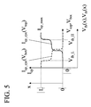
- Figure 5 illustrate an embodiment of a first aspect of the invention
- Figure 6 shows charge-pumping curves for varying top-level or bottom-level according to an embodiment of a first aspect of the invention
- Figure 7 shows the distribution profile of the charge in charge-trapping layer and in the interface traps according an embodiment of a first aspect of the invention
- Figures 8 shows the distribution profile of charge in the trapping-layer for respectively electrons and holes following a program and erase operation according to an embodiment of a first aspect of the invention
- Figure 1 shows a schematic cross-section of a MOSFET-type device. This device (1) comprises a gate electrode (3) separated from the substrate (2) by a gate dielectric (4). Typically the gate electrode is formed from a semiconductor material such as polycrystalline silicon doped to obtain the desired workfunction and/or conductivity. This semiconductor material can be partially or fully silicided as known in the art or even metals, e.g. Al, TiN, TaN, are used. The gate dielectric (8) comprises a dielectric charge-trapping layer (10) such as silicon-nitride, silicon-rich oxide, silicon-oxynitride, an oxide layer comprising nanocrystals of a semiconductor material, e.g. polycrystalline silicon. Optionally this charge-trapping layer can be separated from the substrate (2) by another dielectric layer (11) with low or no trapping capabilities, e.g. silicon-oxide. Another layer (9) in a similar material as layer (11) can be used to separate the charge-trapping layer (10) from the gate electrode (3). The substrate (2) is a semiconductor substrate, e.g. silicon, silicon-on-insulator (SOI), germanium-on-insulator (GOI). Adjacent to the stack of gate electrode (3) and gate dielectric (4) sidewall spacers (5) formed in a dielectric material such as silicon-oxide, silicon-oxynitride, silicon-carbide, can be present. Aligned to this stack source (6) and drain regions (7) are formed in the substrate (2). The source (6) and drain regions (7) are of an opposite conductivity type as the substrate (2). The source (6) and drain regions (7) extend under the spacers (5) such that the channel region (8) is contacted. This channel region (8) is under dielectric control of the gate electrode (3). The device of figure 1 can be manufactured using processing steps and materials known to any person skilled in the art of manufacturing semiconductor devices, in particular non-volatile memory devices.
- For the purpose of teaching the invention it is assumed that the device (1) is a nMOS device comprising a polysilicon gate electrode (3), which is n-type doped. Also source (6) and drain (7) regions are n-type doped while the substrate (2) is p-type doped. Sidewall spacers (5) formed in silicon-oxide are present. The gate dielectric (4) consists of a nitride layer used as charge-trapping layer (10) sandwiched between two layers (9, 11) of silicon-oxide. However the invention is not limited to this example. It will be appreciated that there are numerous variations and modifications possible. The device can be a pMOS device comprising device comprising a polysilicon gate electrode (3), which is p-type doped. Also source (6) and drain (7) regions are p-type doped while the substrate (2) is n-type doped. Instead of being a stacked gate device as shown in figure 1a the device can be a split gate device such as the HIMOS memory cell disclosed in
US5,583,811 hereby incorporated by reference in its entirety Accordingly, the description should not be deemed to be limiting in scope. - In general, all methods for extracting the spatial distribution of charge Nnt stored in the charge-trapping layer (10) of the semiconductor device (1) which are discussed below comprise the following steps: determining a varying base-level voltage Vbase charge pumping curve, determining a varying top-level voltage Vtop charge pumping curve, and combining data from the charge pumping curves to obtain the spatial distribution of the stored charge Nnt. This combination of data is done by establishing a relation between a charge pumping current Icp and a calculated channel length Lcalc of the semiconductor device by reconstructing a spatial charge distribution from the charge pumping curves for multiple values of the charge pumping current Icp. From these multiple values of Icp the value is obtained for which the corresponding calculated channel length Lcalc is substantially equal to the effective channel length Leff of the semiconductor device, this charge pumping current Icp being the maximum charge pumping current Icp_max. Finally the spatial distribution Nnt of the charge is extracted by reconstructing the spatial charge distribution from the charge pumping curves using the value of Icp = Icp_max.
- In all embodiments described below, separately the spatial distribution of charges within a charge-trapping layer of a charge-trapping device and traps situated at the interface of this layer is extracted. Preferably this charge-trapping device is a non-volatile charge-trapping memory device.
- A charge-pumping measurement set-up, which can be used in for determining the charge pumping curves, is schematically shown in figure 1a. Source (6), drain (7) and substrate (2) regions are biased to a fixed voltage, preferably 0V or ground. A voltage source, e.g. a pulse generator, is connected to the gate electrode while current is measured at the substrate. This measurement set-up is also known as amplitude-sweep charge-pumping set-up as the amplitude of the voltage pulses applied to the gate electrode is increased during the measurement.
- In the embodiment described below, the measurement sequence comprises two steps: first two charge-pumping measurements are performed on a device used as reference and secondly similar charge-pumping measurements are performed on the device-under-test (DUT).
- The reference device is usually the same as the studied device but in a reference state. The studied device needs to have a monotonic increase or decrease of the threshold voltage along the channel, or at least along the part of the channel, which is subjected to the measurement method, typically half of the channel. In this case, each threshold voltage value corresponds to one point of the charge-pumping curve. The reference state of this device, more precisely the threshold voltage distribution thereof depends on the charge already trapped in the studied device. If the threshold voltage distribution in the studied device increases monotonically, it is better to have the reference state having a similar increase in threshold voltage distribution. For instance, the pristine device can be subjected to a light programming operation resulting in a monotonic increase of the charge in the charge-trapping layer which results in a threshold profile Vth (x) that monotonic varies along the channel as shown in figure 2 by the dotted line Vth_ref(x). In this figure the threshold voltage of the device in the reference state slightly increase near the drain d. The number and distribution of the interface traps should remain essentially unaffected and essentially uniform over the channel. If the threshold voltage distribution monotonically decreases, it is better to have the reference state with also a decreasing threshold voltage distribution. The most natural reference state is in this case the virgin device, where the threshold voltage progressively decreases from the center of the channel to the junction.
- A first charge-pumping measurement, illustrated by figures 1b and 1 c, is performed on the device in the reference state that has not yet been electrically stressed, i.e. the interface trap distribution can be considered uniform along the channel. A first pulse train is applied to the gate electrode (3), whereby each pulse in this pulse train has the same bottom-level Vbot. The amplitude Vp of the pulses increases monotonically with time by increasing the top-level Vtop of the pulses. The exemplary pulse train shown in figure 1 b comprises 9 pulses grouped in sets of 3. The pulses in the first set have the lowest amplitude, the pulses in the second set have a higher amplitude, while the pulses in the last set have the highest amplitude. So the amplitude of the pulse in the pulse sequence or the voltage swing of each pulse increases progressively. The number of pulses in the pulse train, their duty cycle, the amplitude of each pulse, the way the amplitude Vp is increased over the pulse train, e.g. stepwise, gradually, and the upper level Vtop are parameters of choice and can be selected in view of the required accuracy and measurement resolution.
- When the bottom level of the pulse Vbot is below the flatband voltage Vfb_H of the device (1) and the upper level of the pulse Vtop is above the threshold voltage Vth-L of the device (1) accumulation and inversion layers will be successively formed at the interface between the channel (8) and the gate dielectric (4).. Inversion layer electrons from the source (6) and/or drain (7) regions will fill the interface states Nit during the high pulse bias. These interface states thus become negatively charged. When the voltage is dropped below the flatband voltage Vfb_ref(x), accumulation layer holes from the substrate (2) will quickly recombine with the trapped electrons resulting in a charge-pump current Icp.. The charge-pump current is proportional to the pulse frequency and the number of interface states Nit in the inversion region formed in the channel. From this charge-pumping measurement the charge-pump curve Icp (VP) of this device in the reference state is obtained as shown in figure 1c given the current Icp or charge per pulse as function of the top level Vtop of the pulse train. One can change the vertical axis of this curve by replacing Icp with the position x along the channel: no current corresponds to one end of the channel, e.g. source where x = 0, while the maximum Icp_max current corresponds to the other end of the channel, e.g. drain where x = 100% = channel effective length Leff. By rearranging this charge-pumping curve by using the method disclosed by Maarten Rosmeulen et al in paragraph 3.3 of "Characterization of the spatial charge distribution in local charge-trapping memory devices using the charge-pumping technique", Solid-State Electronics journal, volume 48 (2004) p1525-1530, hereby incorporated by reference, a threshold profile curve Vth,ref(x) is obtained showing the change of voltage applied to this device as function of its relative position x with respect to source and drain.
- A second charge-pumping measurement is performed on the device in the reference state. A pulse train is applied to the gate electrode (3), whereby each pulse in this pulse train has the same top-level Vtop. The amplitude Vp of the pulses increases monotonically with time by lowering the bottom-level Vbot of the pulses. The exemplary pulse train shown in figure 1d comprises 9 pulses grouped in sets of 3. The pulses in the first set have the lowest amplitude or voltage swing, the pulses in the second set have a higher amplitude, while the pulses in the last set have the highest amplitude. The number of pulses in the pulse train, their duty cycle, the amplitude of each pulse, the way the amplitude VP is increased over the pulse train, e.g. stepwise, gradually, the upper level Vtop are parameters of choice and can be selected in view of the required accuracy and measurement resolution. This pulse train with fixed top-level Vtop and varying bottom-level Vbot will fill the interface states with electrons during the uptime tup of the pulse and with holes during the downtime tdo of the pulse when Vbot is below the flatband voltage Vfb_H. As long as the lower level Vbot of the pulse is above the flatband voltage Vfb_H, the channel will remain in inversion and the interface traps are always filled with electrons. The channel (8) will switch between inversion and accumulation depending on whether the lower level Vbot of the progressively increased pulse amplitude is above or below this flatband voltage Vfb-H and the interface traps will be alternatively filled with electrons and holes during the charge-pumping measurements. From this charge-pumping measurement the charge-pump curve Icp (VP) of this device in the reference state is obtained as shown in figure 1 e given the current Icp or charge per pulse as function of the bottom level Vbot of the pulse train. One can change the vertical axis of this curve by replacing Icp with the position x along the channel: the maximum Icp_max current corresponds to one end of the channel, e.g. source where x = 0, while no current corresponds to the other end of the channel, e.g. drain where x = 100% = channel effective length Leff. By rearranging this charge-pumping curve by using the method disclosed by Maarten Rosmeulen et al in paragraph 3.3 of "Characterization of the spatial charge distribution in local charge-trapping memory devices using the charge-pumping technique",in Solid-State Electronics journal, volume 48 (2004) p1525-1530, hereby incorporated by reference, a flatband profile curve Vfb,ref(x) is obtained showing the change of voltage applied to this device as function of its relative position x with respect to source and drain.
- A device under test is electrically stressed resulting in charged carriers to be injected into the charge-trapping layer (10). These injected carriers can be positively or negatively charged. In case the device is used as memory cell, one carrier type is used to program the memory cell while the opposite charged carriers are used to erase the memory cell by compensating the distribution profile of the programmed charge. On this device charge-pumping measurements according to the present invention are performed to determine the contribution to the threshold voltage of the charge Qnt stored in the charge-trapping layer (10) and the charge Qit generated by the interface traps Nit. The charge Qnt stored in the charge-trapping layer (10) generates a constant offset of the threshold voltage ΔVth_Qnt, while the offset ΔVth_Qit generated by the charge stored in the interface traps depends on whether positive or negative charge is stored in these interface traps and on the number of interface traps Nit. In inversion the interface traps are filled with electrons causing an upward shift of the threshold voltage, while in accumulation the interface traps are filled with holes causing a downward shift of the threshold voltage. The degradation of a device, e.g. by repetitive electrical stress applied to the device, will change the number of interface traps and hence the threshold voltage offset ΔVth_Qit. A threshold voltage distribution shown in figure 2 can result from negative charge e.g. present in the charge-trapping layer (10) of an nMOS device. A similar figure can be drawn for the flatband voltage distribution of this device. If the device of figure 1 is used as non-volatile memory cell, electrons can be injected into this layer (10) during the step of programming the memory cell, e.g. by channel-hot-electron-injection as is known in the art. Holes can be injected during the step of erasing the memory cell, e.g. by band-to-band tunneling induced hot hole injection as is known in the art. This localized trapped charge, e.g. in the region between x1-d, will result in a local increase Vth_ref(x)-Vth_cyc(x) of the threshold voltage and of the flatband voltage Vfb_ref (x)-Vfb_cyc(x). For the purpose of teaching the invention it assumed that negative charge Qnt is stored in the charge-trapping layer (10) of an nMOS memory cell (1) resulting in positive shift of the threshold voltage and the flatband voltage, i.e. the threshold voltage and flatband voltage become more positive in these locations where the negative charge Qnt is stored. In real devices the threshold voltage distribution along the channel will is not sharply define as suggested in figure 2 but will vary along the channel due to the presence of the junctions and of amongst other the interface traps Nit which are distributed along the channel.
- A first charge-pumping measurement is performed on the device under test. Figure 3a illustrates such a device wherein a number Nnt of negative charged particles (dotted area between position x1 and drain d) is stored in the charge-trapping layer (10) resulting in an increase of the threshold voltage and flatband voltage in the portion x1 to d compared to the portion s to x1. A number of interface states Nit are present (dots in the channel). A pulse train similar to the pulse train of the first measurement on the device in the reference state and illustrated by figure 3b is applied to this device also. As discussed in the first step when measuring the reference device, this pulse train with fixed bottom-level Vbot and varying top-level Vtop will fill the interface states with electrons during the uptime tup of the pulse and with holes during the downtime tdo of the pulse in these locations where the pulse is swept over the corresponding threshold voltage. If the number of interface states or the threshold voltage were uniform over the channel (8), one would obtain the same charge-pump current at each pulse independently of the amplitude of the pulse as long as Vtop is higher than the threshold voltage Vth. If however the threshold voltage is not constant over the channel, as shown in figure 2, with increasing pulse amplitude Vp an increasing portion of the channel will contribute to the charge pump current. As long as the upper level Vtop of the pulse is lower than the local threshold voltage Vth_H the portion of the channel between x1 and d will not contribute to the charge-pumping current. Until then the portion of channel (8) having the higher threshold voltage Vth_H will remain in accumulation and the corresponding interface traps will be always filled with holes as shown in figure 3a by the symbol h+. The portion of the channel (8) having the lower threshold voltage Vth_L will switch between inversion and accumulation depending on whether the upper level Vtop is above or below this lower threshold voltage and the corresponding interface traps will be alternatively filled with electrons and holes during the charge-pumping measurement. If the pulse sequence of figure 3b is applied to the device of figure 3a the channel is scanned from source to drain if the threshold voltage Vth(x) increases monotonically from the source to the drain. If only half of the channel is degraded, Vth(x) needs to be monotonic only on half of the channel. The same procedure as applied to the charge-pumping signal in the first step for extracting the threshold voltage profile Vth (x) from the charge-pumping current for the device under test is applied to this stressed device as illustrated by figure 3c. A relationship between the threshold voltage profile Vth(x) and the location x in the channel can be established by the fact that the increase of the charge-pump current Icp from one location x1 in the channel to another location x2 can be attributed to the number of interface traps Nit present in the channel area between these location. This relationship is expressed as follows:

with q the absolute value of the electron charge, f the frequency of the pulse. In this figure the dotted line indicates the reference charge-pump curve while the solid line indicates the charge-pumping curve obtained on the stressed device. The deviation between both charge-pump curves and hence in the corresponding threshold voltages is induced by the total charge (Qnt+Qit) present, for each point x along the channel, as expressed in the following formula:
with C the capacitance of the dielectric stack (F/cm2), q the absolute value of the electron charge. The concentration of charge in the charge-storage layer Nnt(x) (#/cm2) is positive if electrons are trapped, while the local concentration of interface traps Nit(x) is also in (#/cm2). By varying the top level of the voltage applied on the gate as described in this paragraph classical charge-pumping curves are obtained as is known by a person skilled in the art. During this charge-pumping measurement the threshold voltage and flatband voltage at any given point is determined by the charge at that point: electrons stored in the charge-trapping layer (10) and the holes trapped in the interface states. The shift in threshold voltage is indicated in figure 3c. - A second charge-pumping measurement is performed on this device under test. Figure 4a illustrates such a device wherein a number Nnt of negative charged particles (dotted area between position x1 and drain d) is stored in the charge-trapping layer (10). A number of interface states Nit is present (dots in the channel). A pulse train, similar to the pulse train applied during the second measurement on the device in the reference state, is applied to the gate electrode (3), whereby each pulse in this pulse train has the same top-level VtoP. The amplitude Vp of the pulses increases monotonically with time by lowering the bottom-level Vbot of the pulses. The exemplary pulse train shown in figure 4b comprises 9 pulses grouped in sets of 3. The pulses in the first set have the lowest amplitude or voltage swing, the pulses in the second set have a higher amplitude, while the pulses in the last set have the highest amplitude. The number of pulses in the pulse train, their duty cycle, the amplitude of each pulse, the way the amplitude Vp is increased over the pulse train, e.g. stepwise, gradually, the upper level Vtop are parameters of choice and can be selected in view of the required accuracy and measurement resolution. This pulse train with fixed top-level Vtop and varying bottom-level Vbot will fill the interface states with electrons during the uptime tup of the pulse and with holes during the downtime tdo of the pulse in these locations where the pulse is swept over the corresponding flatband voltage. As long as the lower level Vbot of the pulse is above the local flatband voltage Vfb_L the portion of the channel between x1 and d will remain in inversion and the interface traps are always filled with electrons as shown in figure 4a by the symbol e-. This portion of the channel (8) having the lower flatband voltage Vfb_L will switch between inversion and accumulation depending on whether the lower level Vbot of the progressively increased pulse amplitude is above or below this lower flatband voltage and the corresponding interface traps in this region will be alternatively filled with electrons and holes during the charge-pumping measurements. If the pulse sequence of figure 4b is applied to the device of figure 4a the channel is scanned from drain to source if the flatband voltage Vfb(x) increases monotonically from the source to the drain. The same procedure as applied to the charge-pumping signal in the first step for extracting the flatband voltage Vfb(x) profile from the charge-pumping current for the device under test is applied to this stressed device as illustrated by figure 4c. A relationship between the flatband voltage profile Vfb (x) and the location x in the channel can be established by the fact that the increase of the charge-pump current Icp from one location x1 in the channel to another location x2 can be attributed to the number of interface traps Nit present in the channel area between these location. This relationship is expressed as follows:

with q the absolute value of the electron charge, f the frequency of the pulse. In this figure the dotted line indicates the charge-pump curve of the reference device, while the heavy dotted line indicates the charge-pump curve obtained on the stressed device. The deviation between both charge-pump curves and hence in the corresponding flatband voltages is induced by the total charge (Qnt+Qit) present, for each point x along the channel, as expressed in the following formula:
with C the capacitance of the dielectric stack (4) (F/cm2) and q the absolute value of the electron charge. The concentration of charge in the charge-storage layer Nnt(x) (#/cm2) is positive if electrons are trapped, while the local concentration of interface traps Nit(x) is also in (#/cm2). By varying the bottom level of the voltage pulses applied on the gate as described in this paragraph the charge-pumping curves of figure 4c are obtained. During this charge-pumping measurement the threshold voltage and flatband voltage at any given point is determined by the charge at that point: electrons stored in the charge-trapping layer (10) and the electrons trapped in the interface states. - The charge-pumping curves obtained on the stressed device are compared with the charge-pumping curve of the reference device or unstressed device. The deviation between the reference curves on the one hand and the corresponding stressed curves is due to the overall threshold or flatband voltage variation caused by the charge in the charge-trapping layer (10) and in the interface states. The difference between the two deviations is due to the charge in the interface states only. Figure 5 combines the two charge-pump curves obtained on the stressed device. In both cases the maximum current measured Icp_max is substantially the same, such that for any location x in the channel, the following relationship holds:

- The correlation between the two measurements on the stressed device depend on Icp_max, which makes the results of the extraction very sensitive to this value. Theoretically, the charge-pumping curves saturate completely if the top level of the pulse is high enough (or if the base level of the pulse is low enough, following the type of measurement). The measurements in figure 6 show that the saturation is in reality not perfect, curves slightly continue to increase for high voltages. This causes incertitude on Icp_max. The best choice of Icp_max is explained later in this text.
- Using the data from the charge-pumping measurements with respectively varying top and bottom level performed on the device in the reference state (figure 1c, 1e) and on the cycled device (figure 3c, 4c) and the above equations ([1], [2], [3], [4], [5]) one can determining the contribution of the charge in the charge-trapping layer (10) and of the charge in the interface states to the change in threshold voltage.
- Equations [2] and [4] can combined to yield the following formula:

- Equation [1] can be written as:

- By solving successively equations [6] and [7] from a starting point xo to a final point xend one can find the position xi from equation [7] which corresponds to the interface states Nit(xi) from equation [6]. The profile of charge in the charge-trapping layer can be found by either solving equation [2] or [4].
- The method allows an easy way to check the precision of the extracted profiles. Indeed, the last calculated position xend must correspond to the effective length of the channel:

As explained before, the results are very sensitive to Icp_max. Icp_max is then chosen such as equation [8] is verified. The use of Icp_max as a variable and the addition of the equation [8] allow a higher accuracy on the extracted profiles. This is made possible by the new direct method to solve the equations [5-7]. - In the following paragraph the extraction procedure is discussed in more detail. If the difference (Vth_ref(x)-Vfb_ref(x)) in equation [6] is constant, because the number of interface traps Nit,ref of the device in the reference state is constant and equal to the ratio (Icp_max/Leff), this difference is given by combining the threshold voltage profile and flatband voltage profile given by respectively figure 1c and 1e. For the device in the reference state, equation [5] allows to determine for a selected threshold voltage Vth_cyc the corresponding flatband voltage Vfb_cyc, as the sum of the corresponding charge-pump currents must be equal to the maximum charge-pump current Icp_max. The starting point xo is selected such that the threshold voltage Vth_cyc(xo) is not shifted and the number of interface states Nit(xo) is equal to the number of interface states in the device in the reference state Nit,ref = (Icp_max/ Leff). By directly solving equations [6] and [7] successively for all measurement points in the charge-pump curve from this starting point xi = xo to xi = xend, one can find the position xi from equation [7] which corresponds to the interface states Nit(xi) from equation [6]. The profile of charge in the charge-trapping layer can be found by either solving equation [2] or [4].
- If the difference (Vth_ref (x)-Vfb_ref (x)) in equation [6] is not constant, equations [6] and [7] cannot be solved directly. Both equations are then rewritten in the form "Nit(xi)= " which can be solved numerically.


Hence the extraction technique according to the present invention allows determining the contribution of the charge in the charge-trapping layer (10) and of the charge in the interface states to the change in threshold voltage. - In figure 5 the two charge-pumping curves used in the extraction method of the previous embodiments are shown. Ideally the charge-pumping current Icp reaches a maximum charge-pumping current Icp_max corresponding to a voltage bias Vtop or Vbot wherein the complete area of the channel (8) having a known channel length Leff contributes to the charge-pumping current. For this well-defined maximum charge-pumping current Icp_max one can reconstruct the spatial distribution of charge Nnt stored in the charge-trapping layer (10) of a semiconductor device (1). However in real measurements the current measured when applying a varying base-level or top-level voltage pulse sequence might not reach a maximum value and will continue to vary with varying pulse voltage. When such charge-pumping curves are obtained one can determine the maximum charge-pumping current Icp_max, corresponding to the complete area of the channel (8) having a known channel length Leff, from the effective charge-pumping curves in various ways some of which are described in the embodiments below.
- In a preferred embodiment of the extraction method, the charge pumping curves are combined as follows. As described before, a relation between the charge pumping current Icp and the calculated channel length Lcalc of the semiconductor device is established. In this embodiment, this is done by selecting on one of the charge pumping curves at least two charge pumping currents Icp and determining the calculated channel length Lcalc corresponding to each of the charge pumping currents Icp by reconstructing the spatial charge distribution for each of the charge pumping currents Icp. In this way, a set of at least two datapoints (Lcalc, Icp) is obtained. From this set of datapoints, the charge pumping current Icp having a channel length substantially equal to the effective length Leff i.e. the maximum charge pumping current Icp_max can be obtained as follows.
- For example, various existing numerical techniques can be used to determine from this set of at least two datapoints (Lcalc, Icp), the datapoint (Lcalc = Leff, lcp = Icp_max). Once can use known numerical analytical techniques such as linear interpolation or binary search to determine this datapoint (Leff, Icp_max). A person skilled in the art will appreciate that the first values of the charge pump current Icp are selected from the upper current range of the measured charge-pumping curve as such selection will speed up the extraction process.
- As an alternative, an analytical function Lcalc (Icp) - Leff = 0 can be determined from the set of at least two datapoints (Lcalc, Icp), and by solving this analytical function the charge pumping current Icp having a channel length substantially equal to the effective length Leff, i.e. the maximum charge pumping current Icp_max, can be determined. Then, the the spatial distribution Nnt of the charge is extracted by reconstructing the spatial charge distribution from the charge pumping curves using the value of Icp = Icp_max. A person skilled in the art will appreciate that the first values of the charge pump current Icp are selected from the upper current range of the measured charge-pumping curve as such selection will speed up the extraction process.
- Another alternative could be to combine the data from the charge pumping curves as follows. Again a relation between the charge pumping current Icp and a calculated channel length Lcalc of the semiconductor device is established by selecting on one of the charge pumping curves a value of the charge pumping current Icp and determining the calculated channel length Lcalc corresponding to this charge pumping current Icp by reconstructing the spatial charge distribution for this charge pumping current Icp. In this embodiment however, the calculated channel length Lcalc is compared with the effective length Leff and in case of a mismatch, a new value for the charge pumping current Icp is determined using the information given by the mismatch, i.e. the selection of the value for the charge pumping current Icp is optimised. This sequence of steps is repeated until the mismatch between the calculated channel length Lcalc and the effective length Leff is substantially zero, in which case this the determined charge pumping current Icp corresponds to the maximum charge pumping current Icp_max. The spatial distribution Nnt of the charge is then extracted by reconstructing the spatial charge distribution from the charge pumping curves using this value of Icp = Icp_max. A person skilled in the art will appreciate that the first values of the charge pump current Icp are selected from the upper current range of the measured charge-pumping curve as such selection will speed up the extraction process.
- In the above extraction methods the determined charge pumping current Icp is said to correspond to the maximum charge pumping current Icp_max, when the difference between the obtained calculated channel length Lcalc and the effective length Leff is less than 2%, preferably less than 1% of the effective channel length Leff.
- Although the extraction methods according to the present application are particular useful for extracting the spatial distribution of charge Nnt stored in the charge-trapping layer (10) of a memory device (1), these extraction methods can be applied to any kind of semiconductor device (1) wherein a dielectric stack (4) is sandwiched between an electrode (3) and a semiconductor region (2). The disclosed extraction methods can be used to the extract charge stored in this dielectric stack (4). For example in a MOSFET, used as logic transistor, charge might be unintentionally incorporated in the gate dielectric (4). Typically this incorporated charge might result from the device operation, e.g. hot carriers, or result from the semiconductor manufacturing process introducing fixed or mobile charge in the gate dielectric. This gate dielectric can be of a single dielectric material such as silicon-oxide, silicon-oxy-nitride, a high-k dielectric such as alumina-oxide, hafnium-oxide, hafnium-silicon-oxide as known in the art. Likewise this gate dielectric can be a stack of dielectric materials, e.g. a high-k dielectric formed upon a silicon-oxide. As is the case for the memory device in the previous embodiments, this charge Nnt will also influence the threshold voltage profile Vth(x) and flatband voltage profile Vfb(x) of the logic transistor. Hence the disclosed extraction methods can also be applied to such logic transistor to determine the spatial distribution of the incorporated charge Nnt.
- In the disclosed extraction methods the spatial charge distribution Nnt is reconstructed from the charge pumping curves by combining data from these charge pumping curves to obtain the spatial distribution. This data from the charge pumping curves can be further combined to obtain a spatial distribution of charge (Nit) in traps present at the interface between the channel (8) and a dielectric stack (4). Hence the present extraction methods also allow determining the spatial distribution of this interface charge Nit, even when charge is present in the dielectric stack (4). The dependency of this interface charge on parameters of the semiconductor process or of device operation can thus more accurately be determined.
- Figures 6 to 8 illustrate a preferred embodiment of the invention.
- Figure 6 shows two sets of charge-pumping curves obtained using respectively the varying top-level and varying-base level pulse sequence described above. The rising curves are obtained using the fixed-bottom/varying top-level pulse sequence. The falling curves are obtained using the fixed-bottom/varying base-level pulse sequence. Each set contains a curve for a reference device, i.e. an unstressed nMOS device with an ONO layer as gate dielectric, and curves for the same nMOS devices (1) that were subjected to respectively 50us, 500us and 10ms of hole injection. Nitride was used as charge-trapping layer. Holes where injected using typical state-of-the art voltage settings: grounding of source and bulk applying -5V to the gate and 5V to the drain. The longer the injection time the more positive charge is stored in the device and the larger the shift in the charge-pumping curve compared to the virgin device.
- From these curves the distribution of the charge in the nitride layer (Nnt) and in the interface traps (Nit) for the respective devices can be extracted with the extraction technique of the invention. Figure 7 shows the corresponding distribution curves. With progressive injection of holes the interface becomes more degraded.
- Using the charge-pumping technique of the present invention allows extracting the distribution profile of the charge in the nitride layer whether electrons or holes are trapped in this nitride layer while, taking the degradation of the interface states into account. Figure 8 shows the distribution profile of the charge in the nitride layer of an nMOS memory cell after a programming operation when electrons are trapped and of the charge in the nitride layer of an nMOS memory cell after an erase operation when holes are trapped. Programming of an nMOS memory cell was done by using typical state-of-the-art voltage settings: grounding of source and substrate, applying 9V to the gate and 3.5V to the drain. Erasing of an nMOS memory cell was done by using typical state-of-the-art voltage settings: grounding of source and substrate, applying -5V to the gate and 5V to the drain.
- Prior art charge-pumping measurement techniques can only extract the electron distribution in a charge-trapping layer (10), e.g. injected therein during the programming operation of a memory cell, by assuming that the interface traps do not affect the threshold voltage. In particular the additional interface traps created when injecting holes in the charge-trapping layer (10), e.g. when erasing a memory cell, makes the extraction of the charge distribution in the charge-trapping layer impossible using these prior art charge-pump techniques due to the sensitivity of the charge-pumping measurement to this interface degradation. By using two charge-pumping measurements with respectively varying top-level and bottom-level, the present invention however allows to extract the dielectric charge and interface traps such that the distribution profile of both electrons and holes in the dielectric layer (10) can be obtained. The thus obtained hole and electron distribution profiles are used for physical understanding and further optimization of charge-trapping devices. The extraction method allows extracting the distribution of the electrons and holes injected into the charge-trapping layer (10) of the memory device and hence to determine voltage settings for maintaining substantially the same charge distribution. By applying this extraction method one can extract not only the distribution of the electrons after a programming operation but also the distribution of holes after an erasing operation. This extraction is more accurate as the degradation of the interface states is taken into account.
Claims (12)
- A method for extracting the spatial distribution of charge (Nnt) stored in a charge-trapping layer (10) of a semiconductor device having a channel (8) underneath the charge trapping layer (4) with an effective length Leff, comprising:a) determining a varying base-level voltage charge pumping curve,b) determining a varying top-level voltage charge pumping curve,c) combining data from the charge pumping curves to obtain the spatial distribution,characterised in that step c) comprises the steps of:d) establishing a relation between a charge pumping current Icp and a calculated channel length Lcalc of the semiconductor device by reconstructing a spatial charge distribution from the charge pumping curves for multiple values of the charge pumping current Icp,e) obtaining from the multiple values of Icp the value for which the corresponding calculated channel length Lcalc is substantially equal to the effective channel length Leff of the semiconductor device,f) reconstructing the spatial charge distribution from the charge pumping curves using the value of Icp obtained in step e).
- A method according to claim 1, characterised in that steps d) to e) comprise:g) selecting on one of the charge pumping curves one value of the charge pumping current Icp,h) determining the calculated channel length Lcalc corresponding to the selected charge pumping current Icp by reconstructing the spatial charge distribution for the charge pumping current Icp,i) comparing the calculated channel length Lcalc with the effective length Leff and in case of a mismatch, determining from the mismatch a new value for the charge pumping current Icp,j) repeating steps h) to i) until the mismatch between the calculated channel length Lcalc and the effective length Leff is substantially zero.
- A method according to claim 1, characterised in that steps d) to e) comprise:k) selecting on one of the charge pumping curves at least two charge pumping currents Icp,I) determining the calculated channel length Lcalc corresponding to each of the selected charge pumping currents Icp by reconstructing the spatial charge distribution for each of the selected charge pumping currents Icp, thereby creating a set of at least two datapoints (Lcalc, Icp),m) determining by interpolation from the set of at least two datapoints the charge pumping current Icp corresponding to a channel length Lcalc substantially equal to the effective length Leff,
- A method according to claim 1, characterised in that steps d) to e) comprise:n) selecting on one of the charge pumping curves at least two charge pumping currents Icp,o) determining the calculated channel length Lcalc corresponding to each of the selected charge pumping currents Icp by reconstructing the spatial charge distribution for each of the selected charge pumping currents Icp, thereby creating a set of at least two datapoints (Lcalc, Icp),p) determining an analytical function Lcalc (Icp) - Leff = 0 from the set of at least two datapoints,q) determining by solving the analytical function the charge pumping current Icp corresponding to a channel length Lcalc substantially equal to the effective length Leff,
- A method according to any one of the previous claims, characterised in that data from the charge pumping curves is further combined to obtain a spatial distribution of charge in traps (Nit) present at the interface between the channel (8) and a dielectric stack (11) which separates the charge trapping layer (10) from the channel (11).
- A method according to any one of the previous claims, characterised in that the method further comprises the initial step of bringing the semiconductor device (1) into a reference state by subjecting it to a light programming operation, resulting in a monotonic increase of the charge in the charge-trapping layer (10) which results in a threshold profile Vth (x) that monotonically varies along the channel (8).
- A method according to claim 6, characterised in that the method is performed at least once on the semiconductor device in the reference state and at least once on the semiconductor device in a cycled state after one or more programming/erase cycles, to determine the contribution of charges remaining in the charge-trapping layer (10) after the one or more programming/erase cycles to the threshold voltage along the channel (8).
- A method according to any one of the previous claims, characterised in that step a) comprises applying a pulse train to a gate electrode (3), which is located above the charge-trapping layer (4) opposite the channel (8), wherein each pulse in this pulse train has the same top-level voltage and the amplitude of the pulses increases monotonically with time by lowering the base-level voltage of the pulses.
- A method according to any one of the previous claims, characterised in that step b) comprises applying a pulse train to a gate electrode (3), which is located above the charge-trapping layer (10) opposite the channel (8), wherein each pulse in this pulse train has the same base-level voltage and the amplitude of the pulses increases monotonically with time by increasing the top-level voltage of the pulses.
- A method according to any of the foregoing claims wherein the difference between the obtained calculated channel length Lcalc and the effective length Leff is less than 1 %.
- A method according to any of the foregoing claims wherein reconstructing a spatial charge distribution from the charge pumping curves comprises:r) selecting a starting point on one of the charge-pumping curves,s) solving the equations

and
from the starting point over a selected portion of the charge-pumping curve, andt) solving at least one of the equations
or
wherein
Vth_ref (x) is the threshold voltage curve of a reference device,
Vfb_ref (x) is the flatband voltage curve of a reference device,
Vth_cyc (x) is the threshold voltage curve of the semiconductor device after at least one program/erase operation,
Vfb_cyc (x) is the flatband voltage curve of the semiconductor device after at least one program/erase operation,
q the absolute value of the electron charge,
Nit(x) is the number interface traps (number/cm2),
Nnt(x) is the number of charge carriers present in the charge-trapping layer (10) (number/cm2),
f is the frequency of the varying-level voltage signal,
Qnt is the charge present in the charge-trapping layer (10) (C/cm2),
Qit is the charge present in the interface traps (C/cm2),
x is a coordinate along the channel of the semiconductor device,
C is the capacitance of the dielectric stack (4) (F/cm2). - A method according to any of the claims 1 to 10 wherein reconstructing a spatial charge distribution from the charge pumping curves comprises:u) selecting a starting point on one of the charge-pumping curves,v) solving the equations

and
from the starting point over a selected portion of the charge-pumping curve, andw) solving at least one of the equationswherein
or
Vth_ref (x) is the threshold voltage curve of a reference device,
Vfb_ref (x) is the flatband voltage curve of a reference device,
Vth_cyc (x) is the threshold voltage curve of the semiconductor device after at least one program/erase operation,
Vfb_cyc (x) is the flatband voltage curve of the semiconductor device after at least one program/erase operation,
q the absolute value of the electron charge,
Δ Nit(x) is the number interface traps (number/cm2),
Δ Nnt(x) is the number of charge carriers present in the charge-trapping layer (10) (number/cm2),
f is the frequency of the varying-level voltage signal,
Qnt is the charge present in the charge-trapping layer (10) (C/cm2),
Qit is the charge present in the interface traps (C/cm2),
x is a coordinate along the channel of the semiconductor device,
C is the capacitance of the dielectric stack (4) (F/cm2).
Priority Applications (11)
| Application Number | Priority Date | Filing Date | Title |
|---|---|---|---|
| DE602005009937T DE602005009937D1 (en) | 2005-06-03 | 2005-10-14 | Extraction method for load distribution in a semiconductor device |
| AT05109600T ATE409350T1 (en) | 2005-06-03 | 2005-10-14 | EXTRACTION PROCESS FOR LOAD DISTRIBUTION IN A SEMICONDUCTOR COMPONENT |
| EP05109600A EP1732080B1 (en) | 2005-06-03 | 2005-10-14 | Method for extracting the distribution of charge stored in a semiconductor device |
| JP2006154455A JP5148076B2 (en) | 2005-06-03 | 2006-06-02 | Method for extracting the distribution of charge stored in a semiconductor device |
| US11/445,551 US7388785B2 (en) | 2005-06-03 | 2006-06-02 | Method for extracting the distribution of charge stored in a semiconductor device |
| EP06763541A EP1886320B1 (en) | 2005-06-03 | 2006-06-06 | Method for extracting the distribution of charge stored in a semiconductor device |
| PCT/EP2006/062944 WO2006128922A1 (en) | 2005-06-03 | 2006-06-06 | Method for extracting the distribution of charge stored in a semiconductor device |
| JP2008514128A JP5191382B2 (en) | 2005-06-03 | 2006-06-06 | Method for extracting distribution of charge accumulated in semiconductor device |
| AT06763541T ATE445901T1 (en) | 2005-06-03 | 2006-06-06 | METHOD FOR EXTRACTING THE CHARGE DISTRIBUTION STORED IN A SEMICONDUCTOR COMPONENT |
| US11/916,796 US7933153B2 (en) | 2005-06-03 | 2006-06-06 | Method for extracting the distribution of charge stored in a semiconductor device |
| DE602006009797T DE602006009797D1 (en) | 2005-06-03 | 2006-06-06 | Method for extracting the load distribution stored in a semi-conductor component |
Applications Claiming Priority (3)
| Application Number | Priority Date | Filing Date | Title |
|---|---|---|---|
| US68707605P | 2005-06-03 | 2005-06-03 | |
| US70485905P | 2005-08-01 | 2005-08-01 | |
| EP05109600A EP1732080B1 (en) | 2005-06-03 | 2005-10-14 | Method for extracting the distribution of charge stored in a semiconductor device |
Publications (2)
| Publication Number | Publication Date |
|---|---|
| EP1732080A1 true EP1732080A1 (en) | 2006-12-13 |
| EP1732080B1 EP1732080B1 (en) | 2008-09-24 |
Family
ID=36975251
Family Applications (2)
| Application Number | Title | Priority Date | Filing Date |
|---|---|---|---|
| EP05109600A Expired - Lifetime EP1732080B1 (en) | 2005-06-03 | 2005-10-14 | Method for extracting the distribution of charge stored in a semiconductor device |
| EP06763541A Not-in-force EP1886320B1 (en) | 2005-06-03 | 2006-06-06 | Method for extracting the distribution of charge stored in a semiconductor device |
Family Applications After (1)
| Application Number | Title | Priority Date | Filing Date |
|---|---|---|---|
| EP06763541A Not-in-force EP1886320B1 (en) | 2005-06-03 | 2006-06-06 | Method for extracting the distribution of charge stored in a semiconductor device |
Country Status (6)
| Country | Link |
|---|---|
| US (2) | US7388785B2 (en) |
| EP (2) | EP1732080B1 (en) |
| JP (2) | JP5148076B2 (en) |
| AT (2) | ATE409350T1 (en) |
| DE (2) | DE602005009937D1 (en) |
| WO (1) | WO2006128922A1 (en) |
Families Citing this family (11)
| Publication number | Priority date | Publication date | Assignee | Title |
|---|---|---|---|---|
| DE602005019864D1 (en) * | 2005-06-03 | 2010-04-22 | Imec | A method of controlling a nonvolatile charge arrest memory device and methods of determining program / erase parameters |
| JP2007073969A (en) * | 2005-09-07 | 2007-03-22 | Samsung Electronics Co Ltd | Charge trap memory device and method of manufacturing the same |
| US8394683B2 (en) | 2008-01-15 | 2013-03-12 | Micron Technology, Inc. | Methods of forming semiconductor constructions, and methods of forming NAND unit cells |
| US8841682B2 (en) * | 2009-08-27 | 2014-09-23 | Cree, Inc. | Transistors with a gate insulation layer having a channel depleting interfacial charge and related fabrication methods |
| US8941171B2 (en) * | 2010-07-02 | 2015-01-27 | Micron Technology, Inc. | Flatband voltage adjustment in a semiconductor device |
| JP5801049B2 (en) * | 2010-12-28 | 2015-10-28 | ラピスセミコンダクタ株式会社 | Method for writing data to semiconductor memory device and semiconductor memory device |
| CN102163568B (en) * | 2011-03-07 | 2012-10-10 | 北京大学 | Method for extracting charge distribution of metal oxide semiconductor (MOS) tube along channel |
| US8832619B2 (en) * | 2013-01-28 | 2014-09-09 | Taiwan Semiconductor Manufacturing Co., Ltd. | Analytical model for predicting current mismatch in metal oxide semiconductor arrays |
| KR102341157B1 (en) * | 2017-02-10 | 2021-12-21 | 글로벌웨이퍼스 씨오., 엘티디. | Methods for evaluating semiconductor structures |
| KR102783321B1 (en) | 2020-08-25 | 2025-03-20 | 삼성디스플레이 주식회사 | Display device and method of driving the same |
| CN121389677B (en) * | 2025-12-26 | 2026-03-24 | 兰州理工大学 | Calculation method of space charge distribution based on tunneling effect and limited hole extraction |
Citations (2)
| Publication number | Priority date | Publication date | Assignee | Title |
|---|---|---|---|---|
| US5583811A (en) | 1991-01-31 | 1996-12-10 | Interuniversitair Micro-Elektronica Centrum Vzw | Transistor structure for erasable and programmable semiconductor memory devices |
| WO1999007000A2 (en) | 1997-08-01 | 1999-02-11 | Saifun Semiconductors Ltd. | Two bit eeprom using asymmetrical charge trapping |
Family Cites Families (14)
| Publication number | Priority date | Publication date | Assignee | Title |
|---|---|---|---|---|
| JP3247396B2 (en) * | 1991-03-29 | 2002-01-15 | 株式会社東芝 | Evaluation method of semiconductor device |
| IL125604A (en) * | 1997-07-30 | 2004-03-28 | Saifun Semiconductors Ltd | Non-volatile electrically erasable and programmble semiconductor memory cell utilizing asymmetrical charge |
| US6331953B1 (en) | 2000-02-16 | 2001-12-18 | Advanced Micro Devices | Intelligent ramped gate and ramped drain erasure for non-volatile memory cells |
| US6490204B2 (en) | 2000-05-04 | 2002-12-03 | Saifun Semiconductors Ltd. | Programming and erasing methods for a reference cell of an NROM array |
| US6396741B1 (en) | 2000-05-04 | 2002-05-28 | Saifun Semiconductors Ltd. | Programming of nonvolatile memory cells |
| US6928001B2 (en) | 2000-12-07 | 2005-08-09 | Saifun Semiconductors Ltd. | Programming and erasing methods for a non-volatile memory cell |
| US6801453B2 (en) * | 2002-04-02 | 2004-10-05 | Macronix International Co., Ltd. | Method and apparatus of a read scheme for non-volatile memory |
| KR100542701B1 (en) | 2003-11-18 | 2006-01-11 | 주식회사 하이닉스반도체 | Threshold Voltage Measurement Method for NAND Flash Memory Devices |
| US7151692B2 (en) * | 2004-01-27 | 2006-12-19 | Macronix International Co., Ltd. | Operation scheme for programming charge trapping non-volatile memory |
| US7075828B2 (en) | 2004-04-26 | 2006-07-11 | Macronix International Co., Intl. | Operation scheme with charge balancing erase for charge trapping non-volatile memory |
| US7345920B2 (en) | 2004-09-09 | 2008-03-18 | Macronix International Co., Ltd. | Method and apparatus for sensing in charge trapping non-volatile memory |
| US20060113586A1 (en) * | 2004-11-29 | 2006-06-01 | Macronix International Co., Ltd. | Charge trapping dielectric structure for non-volatile memory |
| JP2006196650A (en) * | 2005-01-13 | 2006-07-27 | Sharp Corp | Semiconductor nonvolatile memory device and erasing method thereof |
| DE602005019864D1 (en) | 2005-06-03 | 2010-04-22 | Imec | A method of controlling a nonvolatile charge arrest memory device and methods of determining program / erase parameters |
-
2005
- 2005-10-14 DE DE602005009937T patent/DE602005009937D1/en not_active Expired - Lifetime
- 2005-10-14 EP EP05109600A patent/EP1732080B1/en not_active Expired - Lifetime
- 2005-10-14 AT AT05109600T patent/ATE409350T1/en not_active IP Right Cessation
-
2006
- 2006-06-02 JP JP2006154455A patent/JP5148076B2/en not_active Expired - Fee Related
- 2006-06-02 US US11/445,551 patent/US7388785B2/en active Active
- 2006-06-06 DE DE602006009797T patent/DE602006009797D1/en active Active
- 2006-06-06 AT AT06763541T patent/ATE445901T1/en not_active IP Right Cessation
- 2006-06-06 US US11/916,796 patent/US7933153B2/en not_active Expired - Fee Related
- 2006-06-06 JP JP2008514128A patent/JP5191382B2/en not_active Expired - Fee Related
- 2006-06-06 EP EP06763541A patent/EP1886320B1/en not_active Not-in-force
- 2006-06-06 WO PCT/EP2006/062944 patent/WO2006128922A1/en not_active Ceased
Patent Citations (2)
| Publication number | Priority date | Publication date | Assignee | Title |
|---|---|---|---|---|
| US5583811A (en) | 1991-01-31 | 1996-12-10 | Interuniversitair Micro-Elektronica Centrum Vzw | Transistor structure for erasable and programmable semiconductor memory devices |
| WO1999007000A2 (en) | 1997-08-01 | 1999-02-11 | Saifun Semiconductors Ltd. | Two bit eeprom using asymmetrical charge trapping |
Non-Patent Citations (6)
Also Published As
| Publication number | Publication date |
|---|---|
| JP5191382B2 (en) | 2013-05-08 |
| ATE409350T1 (en) | 2008-10-15 |
| US20060284082A1 (en) | 2006-12-21 |
| JP2006352111A (en) | 2006-12-28 |
| WO2006128922A1 (en) | 2006-12-07 |
| JP2008546194A (en) | 2008-12-18 |
| EP1886320A1 (en) | 2008-02-13 |
| ATE445901T1 (en) | 2009-10-15 |
| US7388785B2 (en) | 2008-06-17 |
| EP1886320B1 (en) | 2009-10-14 |
| US7933153B2 (en) | 2011-04-26 |
| DE602005009937D1 (en) | 2008-11-06 |
| EP1732080B1 (en) | 2008-09-24 |
| JP5148076B2 (en) | 2013-02-20 |
| US20090135652A1 (en) | 2009-05-28 |
| DE602006009797D1 (en) | 2009-11-26 |
Similar Documents
| Publication | Publication Date | Title |
|---|---|---|
| US20090141563A1 (en) | Method for Operating a Non-Volatile Charge-Trapping Memory Device and Method for Determining Programming/Erase Conditions | |
| KR100953373B1 (en) | Noise Reduction Techniques for Transistors and Small Devices Using Temporal Shake | |
| JP3863921B2 (en) | Floating gate memory programming method | |
| JP4674239B2 (en) | Multi-level ONO flash program algorithm for threshold width adjustment | |
| US6212100B1 (en) | Nonvolatile memory cell and method for programming and/or verifying the same | |
| EP1732080B1 (en) | Method for extracting the distribution of charge stored in a semiconductor device | |
| US8009482B2 (en) | High temperature methods for enhancing retention characteristics of memory devices | |
| EP1638110A1 (en) | Method and apparatus for operating a string of charge trapping memory cells | |
| JPH0991980A (en) | Method for programming of nonvolatile memory | |
| US20080137418A1 (en) | Method and Apparatus for Sensing In Charge Trapping Non-Volatile Memory | |
| EP1010182A2 (en) | Two bit non-volatile electrically erasable and programmable semiconductor memory cell utilizing asymmetrical charge trapping | |
| US20080158966A1 (en) | Variable Program and Program Verification Methods for a Virtual Ground Memory in Easing Buried Drain Contacts | |
| Rosmeulen et al. | Characterization of the spatial charge distribution in local charge-trapping memory devices using the charge-pumping technique | |
| Furnemont et al. | Cycling behavior of nitride charge profile in NROM-type memory cells | |
| Wrazien et al. | Characterizing damage to ONO dielectrics induced during programming SONOS/NROMTM non-volatile semiconductor memory (NVSM) devices | |
| CN103761989B (en) | Single charging techniques is utilized to measure the method for local hole distribution in SONOS storer | |
| von Emden et al. | A modified constant field charge pumping method for sensitive profiling of near-junction charges | |
| Lorenzini et al. | Lateral Distribution of Electrons Trapped in Nitride Layers |
Legal Events
| Date | Code | Title | Description |
|---|---|---|---|
| PUAI | Public reference made under article 153(3) epc to a published international application that has entered the european phase |
Free format text: ORIGINAL CODE: 0009012 |
|
| AK | Designated contracting states |
Kind code of ref document: A1 Designated state(s): AT BE BG CH CY CZ DE DK EE ES FI FR GB GR HU IE IS IT LI LT LU LV MC NL PL PT RO SE SI SK TR |
|
| AX | Request for extension of the european patent |
Extension state: AL BA HR MK YU |
|
| 17P | Request for examination filed |
Effective date: 20070613 |
|
| AKX | Designation fees paid |
Designated state(s): AT BE BG CH CY CZ DE DK EE ES FI FR GB GR HU IE IS IT LI LT LU LV MC NL PL PT RO SE SI SK TR |
|
| 17Q | First examination report despatched |
Effective date: 20070730 |
|
| GRAP | Despatch of communication of intention to grant a patent |
Free format text: ORIGINAL CODE: EPIDOSNIGR1 |
|
| GRAS | Grant fee paid |
Free format text: ORIGINAL CODE: EPIDOSNIGR3 |
|
| GRAA | (expected) grant |
Free format text: ORIGINAL CODE: 0009210 |
|
| AK | Designated contracting states |
Kind code of ref document: B1 Designated state(s): AT BE BG CH CY CZ DE DK EE ES FI FR GB GR HU IE IS IT LI LT LU LV MC NL PL PT RO SE SI SK TR |
|
| REG | Reference to a national code |
Ref country code: GB Ref legal event code: FG4D |
|
| REG | Reference to a national code |
Ref country code: CH Ref legal event code: EP |
|
| REG | Reference to a national code |
Ref country code: IE Ref legal event code: FG4D |
|
| REF | Corresponds to: |
Ref document number: 602005009937 Country of ref document: DE Date of ref document: 20081106 Kind code of ref document: P |
|
| PG25 | Lapsed in a contracting state [announced via postgrant information from national office to epo] |
Ref country code: LT Free format text: LAPSE BECAUSE OF FAILURE TO SUBMIT A TRANSLATION OF THE DESCRIPTION OR TO PAY THE FEE WITHIN THE PRESCRIBED TIME-LIMIT Effective date: 20080924 |
|
| PG25 | Lapsed in a contracting state [announced via postgrant information from national office to epo] |
Ref country code: FI Free format text: LAPSE BECAUSE OF FAILURE TO SUBMIT A TRANSLATION OF THE DESCRIPTION OR TO PAY THE FEE WITHIN THE PRESCRIBED TIME-LIMIT Effective date: 20080924 Ref country code: LV Free format text: LAPSE BECAUSE OF FAILURE TO SUBMIT A TRANSLATION OF THE DESCRIPTION OR TO PAY THE FEE WITHIN THE PRESCRIBED TIME-LIMIT Effective date: 20080924 Ref country code: AT Free format text: LAPSE BECAUSE OF FAILURE TO SUBMIT A TRANSLATION OF THE DESCRIPTION OR TO PAY THE FEE WITHIN THE PRESCRIBED TIME-LIMIT Effective date: 20080924 Ref country code: SI Free format text: LAPSE BECAUSE OF FAILURE TO SUBMIT A TRANSLATION OF THE DESCRIPTION OR TO PAY THE FEE WITHIN THE PRESCRIBED TIME-LIMIT Effective date: 20080924 |
|
| NLV1 | Nl: lapsed or annulled due to failure to fulfill the requirements of art. 29p and 29m of the patents act | ||
| PG25 | Lapsed in a contracting state [announced via postgrant information from national office to epo] |
Ref country code: BE Free format text: LAPSE BECAUSE OF FAILURE TO SUBMIT A TRANSLATION OF THE DESCRIPTION OR TO PAY THE FEE WITHIN THE PRESCRIBED TIME-LIMIT Effective date: 20080924 |
|
| PG25 | Lapsed in a contracting state [announced via postgrant information from national office to epo] |
Ref country code: ES Free format text: LAPSE BECAUSE OF FAILURE TO SUBMIT A TRANSLATION OF THE DESCRIPTION OR TO PAY THE FEE WITHIN THE PRESCRIBED TIME-LIMIT Effective date: 20090104 Ref country code: BG Free format text: LAPSE BECAUSE OF FAILURE TO SUBMIT A TRANSLATION OF THE DESCRIPTION OR TO PAY THE FEE WITHIN THE PRESCRIBED TIME-LIMIT Effective date: 20081224 |
|
| PG25 | Lapsed in a contracting state [announced via postgrant information from national office to epo] |
Ref country code: CZ Free format text: LAPSE BECAUSE OF FAILURE TO SUBMIT A TRANSLATION OF THE DESCRIPTION OR TO PAY THE FEE WITHIN THE PRESCRIBED TIME-LIMIT Effective date: 20080924 Ref country code: PT Free format text: LAPSE BECAUSE OF FAILURE TO SUBMIT A TRANSLATION OF THE DESCRIPTION OR TO PAY THE FEE WITHIN THE PRESCRIBED TIME-LIMIT Effective date: 20090224 Ref country code: SK Free format text: LAPSE BECAUSE OF FAILURE TO SUBMIT A TRANSLATION OF THE DESCRIPTION OR TO PAY THE FEE WITHIN THE PRESCRIBED TIME-LIMIT Effective date: 20080924 Ref country code: RO Free format text: LAPSE BECAUSE OF FAILURE TO SUBMIT A TRANSLATION OF THE DESCRIPTION OR TO PAY THE FEE WITHIN THE PRESCRIBED TIME-LIMIT Effective date: 20080924 Ref country code: IS Free format text: LAPSE BECAUSE OF FAILURE TO SUBMIT A TRANSLATION OF THE DESCRIPTION OR TO PAY THE FEE WITHIN THE PRESCRIBED TIME-LIMIT Effective date: 20090124 Ref country code: MC Free format text: LAPSE BECAUSE OF NON-PAYMENT OF DUE FEES Effective date: 20081031 Ref country code: NL Free format text: LAPSE BECAUSE OF FAILURE TO SUBMIT A TRANSLATION OF THE DESCRIPTION OR TO PAY THE FEE WITHIN THE PRESCRIBED TIME-LIMIT Effective date: 20080924 |
|
| REG | Reference to a national code |
Ref country code: IE Ref legal event code: MM4A |
|
| PG25 | Lapsed in a contracting state [announced via postgrant information from national office to epo] |
Ref country code: EE Free format text: LAPSE BECAUSE OF FAILURE TO SUBMIT A TRANSLATION OF THE DESCRIPTION OR TO PAY THE FEE WITHIN THE PRESCRIBED TIME-LIMIT Effective date: 20080924 Ref country code: DK Free format text: LAPSE BECAUSE OF FAILURE TO SUBMIT A TRANSLATION OF THE DESCRIPTION OR TO PAY THE FEE WITHIN THE PRESCRIBED TIME-LIMIT Effective date: 20080924 |
|
| PLBE | No opposition filed within time limit |
Free format text: ORIGINAL CODE: 0009261 |
|
| STAA | Information on the status of an ep patent application or granted ep patent |
Free format text: STATUS: NO OPPOSITION FILED WITHIN TIME LIMIT |
|
| RAP2 | Party data changed (patent owner data changed or rights of a patent transferred) |
Owner name: IMEC |
|
| PG25 | Lapsed in a contracting state [announced via postgrant information from national office to epo] |
Ref country code: IT Free format text: LAPSE BECAUSE OF FAILURE TO SUBMIT A TRANSLATION OF THE DESCRIPTION OR TO PAY THE FEE WITHIN THE PRESCRIBED TIME-LIMIT Effective date: 20080924 |
|
| 26N | No opposition filed |
Effective date: 20090625 |
|
| PG25 | Lapsed in a contracting state [announced via postgrant information from national office to epo] |
Ref country code: IE Free format text: LAPSE BECAUSE OF NON-PAYMENT OF DUE FEES Effective date: 20081014 |
|
| PG25 | Lapsed in a contracting state [announced via postgrant information from national office to epo] |
Ref country code: SE Free format text: LAPSE BECAUSE OF FAILURE TO SUBMIT A TRANSLATION OF THE DESCRIPTION OR TO PAY THE FEE WITHIN THE PRESCRIBED TIME-LIMIT Effective date: 20081224 |
|
| PG25 | Lapsed in a contracting state [announced via postgrant information from national office to epo] |
Ref country code: PL Free format text: LAPSE BECAUSE OF FAILURE TO SUBMIT A TRANSLATION OF THE DESCRIPTION OR TO PAY THE FEE WITHIN THE PRESCRIBED TIME-LIMIT Effective date: 20080924 |
|
| REG | Reference to a national code |
Ref country code: CH Ref legal event code: PL |
|
| PG25 | Lapsed in a contracting state [announced via postgrant information from national office to epo] |
Ref country code: LU Free format text: LAPSE BECAUSE OF NON-PAYMENT OF DUE FEES Effective date: 20081014 Ref country code: HU Free format text: LAPSE BECAUSE OF FAILURE TO SUBMIT A TRANSLATION OF THE DESCRIPTION OR TO PAY THE FEE WITHIN THE PRESCRIBED TIME-LIMIT Effective date: 20090325 Ref country code: CY Free format text: LAPSE BECAUSE OF FAILURE TO SUBMIT A TRANSLATION OF THE DESCRIPTION OR TO PAY THE FEE WITHIN THE PRESCRIBED TIME-LIMIT Effective date: 20080924 |
|
| PG25 | Lapsed in a contracting state [announced via postgrant information from national office to epo] |
Ref country code: TR Free format text: LAPSE BECAUSE OF FAILURE TO SUBMIT A TRANSLATION OF THE DESCRIPTION OR TO PAY THE FEE WITHIN THE PRESCRIBED TIME-LIMIT Effective date: 20080924 |
|
| PG25 | Lapsed in a contracting state [announced via postgrant information from national office to epo] |
Ref country code: CH Free format text: LAPSE BECAUSE OF NON-PAYMENT OF DUE FEES Effective date: 20091031 Ref country code: GR Free format text: LAPSE BECAUSE OF FAILURE TO SUBMIT A TRANSLATION OF THE DESCRIPTION OR TO PAY THE FEE WITHIN THE PRESCRIBED TIME-LIMIT Effective date: 20081225 Ref country code: LI Free format text: LAPSE BECAUSE OF NON-PAYMENT OF DUE FEES Effective date: 20091031 |
|
| REG | Reference to a national code |
Ref country code: FR Ref legal event code: PLFP Year of fee payment: 12 |
|
| REG | Reference to a national code |
Ref country code: FR Ref legal event code: PLFP Year of fee payment: 13 |
|
| REG | Reference to a national code |
Ref country code: FR Ref legal event code: PLFP Year of fee payment: 14 |
|
| PGFP | Annual fee paid to national office [announced via postgrant information from national office to epo] |
Ref country code: GB Payment date: 20200921 Year of fee payment: 16 Ref country code: FR Payment date: 20200917 Year of fee payment: 16 |
|
| PGFP | Annual fee paid to national office [announced via postgrant information from national office to epo] |
Ref country code: DE Payment date: 20200917 Year of fee payment: 16 |
|
| REG | Reference to a national code |
Ref country code: DE Ref legal event code: R119 Ref document number: 602005009937 Country of ref document: DE |
|
| GBPC | Gb: european patent ceased through non-payment of renewal fee |
Effective date: 20211014 |
|
| PG25 | Lapsed in a contracting state [announced via postgrant information from national office to epo] |
Ref country code: GB Free format text: LAPSE BECAUSE OF NON-PAYMENT OF DUE FEES Effective date: 20211014 Ref country code: DE Free format text: LAPSE BECAUSE OF NON-PAYMENT OF DUE FEES Effective date: 20220503 |
|
| PG25 | Lapsed in a contracting state [announced via postgrant information from national office to epo] |
Ref country code: FR Free format text: LAPSE BECAUSE OF NON-PAYMENT OF DUE FEES Effective date: 20211031 |