EP1729215A1 - A low area architecture for programming embedded flash memory in a microcontroller - Google Patents
A low area architecture for programming embedded flash memory in a microcontroller Download PDFInfo
- Publication number
- EP1729215A1 EP1729215A1 EP06011187A EP06011187A EP1729215A1 EP 1729215 A1 EP1729215 A1 EP 1729215A1 EP 06011187 A EP06011187 A EP 06011187A EP 06011187 A EP06011187 A EP 06011187A EP 1729215 A1 EP1729215 A1 EP 1729215A1
- Authority
- EP
- European Patent Office
- Prior art keywords
- isp
- core
- microcontroller
- low area
- controller
- Prior art date
- Legal status (The legal status is an assumption and is not a legal conclusion. Google has not performed a legal analysis and makes no representation as to the accuracy of the status listed.)
- Withdrawn
Links
Images


Classifications
-
- G—PHYSICS
- G06—COMPUTING OR CALCULATING; COUNTING
- G06F—ELECTRIC DIGITAL DATA PROCESSING
- G06F9/00—Arrangements for program control, e.g. control units
- G06F9/06—Arrangements for program control, e.g. control units using stored programs, i.e. using an internal store of processing equipment to receive or retain programs
- G06F9/44—Arrangements for executing specific programs
- G06F9/4401—Bootstrapping
- G06F9/4403—Processor initialisation
-
- G—PHYSICS
- G06—COMPUTING OR CALCULATING; COUNTING
- G06F—ELECTRIC DIGITAL DATA PROCESSING
- G06F8/00—Arrangements for software engineering
- G06F8/60—Software deployment
Definitions
- This invention relates to a low area architecture for embedded flash programming memories in microcontrollers.
- the invention relates to a low area architecture for programming a flash memory embedded in microcontrollers comprising a microcontroller core, an embedded flash memory portion, an input/output port and an interface between said core and said memory portion
- microcontrollers with embedded flash memories are widely used today in all applications from home appliances to automotive.
- the embedded flash memory is very useful in system programming which means that the application developer can update program code inside the embedded flash in the microcontroller without removing it from the board through a serial link connection with the programmer (i.e. the PC). In this way the application developer can modify quickly the application program until it works properly.
- a micro with an embedded flash memory is represented with 10; six pins are indicated on the right side of the microcontroller and identified as VDD, IPSEL, VSS, RESET, ISPCLK, ISPDATA. Those pins are used to connect the microcontroller with a programming system through the port connection indicated with 2.
- the system generally include a RAM, a ROM, a Flash and a CORE.
- the ROM is used to contain a boot program but it can generally be directly included in a reserved part of a flash memory portion.
- the program stored in ROM is previously written by the device manufacturer.
- the microcontroller embedded flash memory can be programmed: the boot program stored in the ROM is used to configure the ports of the system during start-up phase and to load the RAM memory.
- the programmer begins a procedure, after the RESET pin is released, to put the microcontroller in an ISP mode.
- ISP mode is indicated a programming phase of the microcontroller.
- the microcontroller executes the boot program located in the embedded ROM in order to configure the I/O port of the serial link (ISPDATA, ISPCLK) and to load the bootstrap program in the RAM.
- microcontroller CORE fetches, decodes and executes the bootstrap program code from RAM and reads data through the serial link to program flash memory.
- the boot ROM When the microcontroller is in the ISP mode the boot ROM is executed through the ISPDATA in order to read and load the boot-strap program in the RAM. Then the control jumps to the RAM to execute the boot-strap program.
- the boot-strap program reads data through the serial link and programs the Flash memory and the option bytes.
- the device comprises input/output ports and four additional pins, TDI, TDO, TCK, TMS, linked to a TAP controller that is in communication with a core.
- the core is involved both in normal mode execution and in programming mode execution. In this way, it is not possible to use the core in normal mode execution, as instance for executing code on a first memory, while the TAP controller is executing in programming mode, for example on second memory or on an additional device.
- Another aim of the present invention is that of providing an architecture for embedded flash programming not based on a ROM and structured to at least reduce internal switch noise when switching off the CORE during programming phase and to reduce flash memory programming time avoiding downloading code in RAM through boot ROM execution.
- the system architecture is free from ROM to improve not only the performance but also for solving the testing problems related to ROM and to achieve a system full scan testable.
- the manufacturer doesn't need to previously store a boot program in ROM or in a dedicated part of the Flash.
- a standard serial link protocol is used to interface the microcontroller instead of a non standard protocol as it will be clear in the following more detailed description.
- FIG. 4 Shown in Figure 4 is globally and schematically shown a microcontroller 10 with an embedded flash memory 1.
- the invention provides a simplified architecture for embedded flash programming that substitutes the ROM functionality through a digital ISP controller able to work with standard protocol link and without creating internal switch noise switching off the microcontroller core during programming phase.
- pins More in particular on the left side of Figure 4, six pins are indicated: RESET, SDA, SCL, VSS, VDD, IPSEL. Two of these pins are connected directly with the I2C serial interface indicated with 2 which is a peripheral already embedded into the device for normal mode operation.
- the I2C peripheral is connected through the DATA_BUS 3 to the ISP controller 4 and to a multiplexer MUX indicated with 5.
- the memory interface 6 is connected to the ISP controller 4 through a mem_address line connection 7 and to the CORE 8 through a mem_addr_core line connection 11.
- a ROM is not required to set up the microcontroller and, as a consequence, transferring the boot program from ROM to RAM is not requested for subsequent execution.
- the register file 9 is connected to the MUX 5 and to the memory interface 6 while the flash memory 1 is connected to the MUX 5 and the memory interface 6.
- the microcontroller After connecting ports as in Figure 1 and releasing RESET pin as known, the microcontroller enters in ISP mode and is managed by the digital ISP controller 4 instead of CORE 8 as happens in normal mode.
- the digital ISP controller 4 is a very small Finite State Machine and its contribution to total area and complexity is negligible.
- the digital ISP controller 4 When in ISP mode, the digital ISP controller 4 configures the I/O ports. After that, it manages the standard I2C 2 serial links SDA and SCL and waits for command from programmer.
- the ISP controller 4 decodes these commands, sends address (mem_address), data (DATA_BUS) and read/write signals (rd, wr, wen, csn) to memory interface in order to program flash memory and option bytes as shown in Figure 4.
- ISP controller 4 provides address and read/write signals for Register file 9 and Memory 6 only in ISP mode while in normal mode they are provided by the CORE 8 (through mem_addr_core, wen_core, csn_core, rd_core and wr_core link).
- a MUX stage is present inside memory interface to select, depending on the microcontroller mode, if the CORE 8 or ISP controller 4 are generating flash and register file addresses.
- the ISP controller 4 If the microcontroller is in ISP mode, the ISP controller 4 generates flash_address directed to Flash memory 1, RF_adrress directed to Register File 9, read/write signals wen_RF and csn_RF also directed to Register File 9 and prg and erase signals directed to Flash Memory 1.
- the CORE is responsible to generate and address the addresses described above.
- data can came from the CORE 8 (through data_core) or from ISP controller 4 (DATA_BUS) in ISP mode.
- the other input of the MUX is data coming from Register Files that needs to be swapped on flash during BlockWrite command when the ISP controller first loads the 64 bytes on Register Files, then swaps them on flash.
- the ISP controller is independent by the CORE, the low area architecture supporting a contemporary execution of the ISP controller in programming mode and the CORE in normal mode.
- the ISP controller is connected to a standard input/output port comprising only two pins, so that no additional peripheral intended to be used in programming mode and requiring additional pins are needed.
Landscapes
- Engineering & Computer Science (AREA)
- Software Systems (AREA)
- Theoretical Computer Science (AREA)
- General Engineering & Computer Science (AREA)
- Physics & Mathematics (AREA)
- General Physics & Mathematics (AREA)
- Computer Security & Cryptography (AREA)
- Read Only Memory (AREA)
- Microcomputers (AREA)
Abstract
The present invention relates to a low area architecture for embedded programming flash memory portions in microcontrollers through the substitution of the ROM/RAM/CORE functionality with a digital ISP controller implemented in a Finite State Machine and a I2C standard peripheral. More in particular the invention provides that, after connecting ports of an embedded flash memory and releasing RESET pin, the microcontroller enters in a particular working modality and it is managed by the digital ISP controller instead of the CORE.
According to the invention, a ROM is not required to set up the microcontroller and in consequence the transferring of the boot program from ROM to RAM is not requested for subsequent execution. The patent proposal shows an architecture for embedded flash programming that substitute the ROM through a digital controller able to work with standard protocol link and without creating internal switch noise switching off the CORE during programming phase.
According to the invention, a ROM is not required to set up the microcontroller and in consequence the transferring of the boot program from ROM to RAM is not requested for subsequent execution. The patent proposal shows an architecture for embedded flash programming that substitute the ROM through a digital controller able to work with standard protocol link and without creating internal switch noise switching off the CORE during programming phase.
Description
- This invention relates to a low area architecture for embedded flash programming memories in microcontrollers.
- More in particular, but not exclusively, the invention relates to a low area architecture for programming a flash memory embedded in microcontrollers comprising a microcontroller core, an embedded flash memory portion, an input/output port and an interface between said core and said memory portion
- The following description relates to this specific field of application with the only purpose to make the illustration easier to understand.
- As it is well known in this technical field, microcontrollers with embedded flash memories are widely used today in all applications from home appliances to automotive.
- The embedded flash memory is very useful in system programming which means that the application developer can update program code inside the embedded flash in the microcontroller without removing it from the board through a serial link connection with the programmer (i.e. the PC). In this way the application developer can modify quickly the application program until it works properly.
- In Figure 1 a micro with an embedded flash memory is represented with 10; six pins are indicated on the right side of the microcontroller and identified as VDD, IPSEL, VSS, RESET, ISPCLK, ISPDATA. Those pins are used to connect the microcontroller with a programming system through the port connection indicated with 2.
- Even if not explicitly shown in Figure 1, the system generally include a RAM, a ROM, a Flash and a CORE. In this kind of microcontroller architecture, the ROM is used to contain a boot program but it can generally be directly included in a reserved part of a flash memory portion. The program stored in ROM is previously written by the device manufacturer.
- Through the above mentioned six pins, the microcontroller embedded flash memory can be programmed: the boot program stored in the ROM is used to configure the ports of the system during start-up phase and to load the RAM memory.
- When the microcontroller is powered on, before using it for any applications, user needs to program the embedded flash memory with program codes, which allows to the microcontroller to work according to the needs.
- In particular, after connecting the ports as shown in Figure 1, the programmer begins a procedure, after the RESET pin is released, to put the microcontroller in an ISP mode. With "ISP mode" is indicated a programming phase of the microcontroller.
- When in ISP mode, the microcontroller executes the boot program located in the embedded ROM in order to configure the I/O port of the serial link (ISPDATA, ISPCLK) and to load the bootstrap program in the RAM.
- Then the microcontroller CORE fetches, decodes and executes the bootstrap program code from RAM and reads data through the serial link to program flash memory.
- Figure 2 is a schematic view of a diagram block describing the transition state of the microcontroller during the start up phase: in particular, to put the microcontroller in the ISP mode the two pins IPSEL and ISPDATA must be configured.
- When the microcontroller is in the ISP mode the boot ROM is executed through the ISPDATA in order to read and load the boot-strap program in the RAM. Then the control jumps to the RAM to execute the boot-strap program. The boot-strap program reads data through the serial link and programs the Flash memory and the option bytes.
- As previously mentioned, in this system architecture the CORE is switched on to fetch, decode and execute bootstrap program from RAM and a dedicated not standard serial link/protocol interface is needed for this matter.
- For example, in the prior art document "Atmega32: 8-bit AVR Microcontroller with 32K Bytes In-System Programmable Flash", in the name of Atmel Corporation, at page 218, a block diagram representing a device architecture is schematically represented.
- The device comprises input/output ports and four additional pins, TDI, TDO, TCK, TMS, linked to a TAP controller that is in communication with a core.
- According to this solution the core is involved both in normal mode execution and in programming mode execution. In this way, it is not possible to use the core in normal mode execution, as instance for executing code on a first memory, while the TAP controller is executing in programming mode, for example on second memory or on an additional device.
- This is a drawback fur the system performances.
- The underlying technical problem of the present invention is to simplify the described embedded flash memory programming system. More particularly the aim is to reduce the configuration complexity of the start-up phase due to the need of interfacing the microcontroller with the embedded memory portions, for reading the ROM, for transferring the boot program in RAM and for the subsequent execution of the program.
- Another aim of the present invention is that of providing an architecture for embedded flash programming not based on a ROM and structured to at least reduce internal switch noise when switching off the CORE during programming phase and to reduce flash memory programming time avoiding downloading code in RAM through boot ROM execution.
- According to one embodiment of the present invention the system architecture is free from ROM to improve not only the performance but also for solving the testing problems related to ROM and to achieve a system full scan testable.
- Also the manufacturer doesn't need to previously store a boot program in ROM or in a dedicated part of the Flash.
- According to a more specific aspect of the invention, a standard serial link protocol is used to interface the microcontroller instead of a non standard protocol as it will be clear in the following more detailed description.
- The features and advantages of the invention will be apparent from the following description of an embodiment thereof, given by way of non-limitative example with reference to the accompanying drawings.
-
- Figure 1 represents in a schematic view a microcontroller with embedded flash memory and a series of pins used for programming the flash memory according to the prior art technique.
- Figure 2 represents a block diagram describing the microcontroller core fetch, decoding and execution phases according to the prior art.
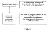
- Figure 3 represents a block diagram describing the digital ISP controller command according to the architecture of the present invention.
- Figure 4 represents the ISP controller decoding commands according to the architecture of the present invention.
- Shown in Figure 4 is globally and schematically shown a
microcontroller 10 with an embeddedflash memory 1. - The invention provides a simplified architecture for embedded flash programming that substitutes the ROM functionality through a digital ISP controller able to work with standard protocol link and without creating internal switch noise switching off the microcontroller core during programming phase.
- More in particular on the left side of Figure 4, six pins are indicated: RESET, SDA, SCL, VSS, VDD, IPSEL. Two of these pins are connected directly with the I2C serial interface indicated with 2 which is a peripheral already embedded into the device for normal mode operation.
- The I2C peripheral is connected through the
DATA_BUS 3 to theISP controller 4 and to a multiplexer MUX indicated with 5. Thememory interface 6 is connected to theISP controller 4 through a mem_address line connection 7 and to the CORE 8 through amem_addr_core line connection 11. - According to the invention, a ROM is not required to set up the microcontroller and, as a consequence, transferring the boot program from ROM to RAM is not requested for subsequent execution.
- The
register file 9 is connected to the MUX 5 and to thememory interface 6 while theflash memory 1 is connected to the MUX 5 and thememory interface 6. - According to the present invention, after connecting ports as in Figure 1 and releasing RESET pin as known, the microcontroller enters in ISP mode and is managed by the
digital ISP controller 4 instead of CORE 8 as happens in normal mode. - The
digital ISP controller 4 is a very small Finite State Machine and its contribution to total area and complexity is negligible. - When in ISP mode, the
digital ISP controller 4 configures the I/O ports. After that, it manages thestandard I2C 2 serial links SDA and SCL and waits for command from programmer. - In this way no ROM is needed and no bootstrap program downloaded and executed in RAM by CORE 8. Program code execution by CORE is replaced, in this architecture, with commands execution by the
digital ISP controller 4, as shown schematically in figure 3. - In the following table the commands received by the
I2C interface 2 and sent toISP 4 controller through thecommon DATA_BUS 3 are reported.Table 1: Command Code Description Block Write 00000001 First erase block currently pointed, then write the 64 bytes ByteWrite 00000010 First erase, then write byte in currently pointed page and offset BlockErase 00000011 Erase the block of the provided offset inside the current page ByteErase 00000100 Erase the byte with the provided offset inside the current page ByteRead 00000101 Read the byte with the provided offset inside the current page FastByteWrite 00001000 Like ByteWrite but without erase GlobalErase 00001001 Erase all first 32K byte Program memory FastBlkWrite 00001011 Like BlockWrite but without erase SetPage 00001100 Update page pointer with provided value ReadData 00001101 Read the currently pointed byte and update address hy one IncBlk 00001111 Update current block pointer by one ReadStatus 00010011 Read current Status Register and exit ISP mode - This table thus reports the commands for the
digital ISP controller 4. - Then the
ISP controller 4 decodes these commands, sends address (mem_address), data (DATA_BUS) and read/write signals (rd, wr, wen, csn) to memory interface in order to program flash memory and option bytes as shown in Figure 4. -
ISP controller 4 provides address and read/write signals for Registerfile 9 andMemory 6 only in ISP mode while in normal mode they are provided by the CORE 8 (through mem_addr_core, wen_core, csn_core, rd_core and wr_core link). - For this purpose a MUX stage is present inside memory interface to select, depending on the microcontroller mode, if the CORE 8 or
ISP controller 4 are generating flash and register file addresses. - If the microcontroller is in ISP mode, the
ISP controller 4 generates flash_address directed to Flashmemory 1, RF_adrress directed to RegisterFile 9, read/write signals wen_RF and csn_RF also directed to RegisterFile 9 and prg and erase signals directed to FlashMemory 1. - If the microcontroller runs in normal mode the CORE is responsible to generate and address the addresses described above.
- The same happens not only for addresses but also for data in the MUX of Figure 4: data can came from the CORE 8 (through data_core) or from ISP controller 4 (DATA_BUS) in ISP mode.
- The other input of the MUX is data coming from Register Files that needs to be swapped on flash during BlockWrite command when the ISP controller first loads the 64 bytes on Register Files, then swaps them on flash.
- ISP is responsible to manage the MUX selector signal. In conclusion we can see that in ISP mode CORE doesn't need tu fetch, decode and execute a bootstrap program from RAM and so it can be switched off reducing internal noise.
- Advantagcously, according to the present invention the ISP controller is independent by the CORE, the low area architecture supporting a contemporary execution of the ISP controller in programming mode and the CORE in normal mode.
- Moreover, the ISP controller is connected to a standard input/output port comprising only two pins, so that no additional peripheral intended to be used in programming mode and requiring additional pins are needed.
Claims (9)
- A Low area architecture (10) for embedded programming flash memories (1) in microcontrollers comprising a microcontroller core (8), an embedded flash memory portion (1), an input/output serial port (2), comprising two pins, and an interface (6) between said core (8) and said memory portion (1) characterized by further comprising a digital ISP controller (4) connected to said input/output serial port (2) and driving said interface (6), said core (8) being independent by said digital ISP controller (4).
- A low area architecture according to claim 1, wherein said ISP controller (4) is connected to said input/output serial port (2) through a DATA_BUS connection (3) and to said memory interface (6) through a mem_address connection.
- A low area architecture according to claim 1, wherein said ISP controller (4) is further connected to a multiplexer (5) through a selector for selecting an ISP or a normal mode execution.
- A low area architecture according to claim 3, wherein said ISP controller (4) is selected in said ISP mode execution or in said normal mode execution when said core (8) is in normal mode execution.
- A low area architecture according to claim 1, wherein said input/output serial port (2) is connected to a couple of serial pins (SDA, SCL) and it is driven by said ISP controller (4) when the system is in ISP mode.
- A low area architecture according to claim 1, wherein said ISP controller (4) is a Finite State Machine.
- A low area architecture according to claim 6, wherein said ISP controller (4) performs internally a programming phase independently from said microcontroller core (8).
- A low area architecture according to claim 1, wherein the code intended for programming said flash memory portion (1) is decoded by said ISP controller (4) from data coming through said serial interface (2).
- A low area architecture according to claim 3, wherein the said multiplexer (5) manages so microcontroller core (8) and said ISP controller (4) for generating flash and register file addresses depending on microcontroller mode.
Applications Claiming Priority (1)
| Application Number | Priority Date | Filing Date | Title |
|---|---|---|---|
| EP05011710 | 2005-05-31 |
Publications (1)
| Publication Number | Publication Date |
|---|---|
| EP1729215A1 true EP1729215A1 (en) | 2006-12-06 |
Family
ID=35355171
Family Applications (1)
| Application Number | Title | Priority Date | Filing Date |
|---|---|---|---|
| EP06011187A Withdrawn EP1729215A1 (en) | 2005-05-31 | 2006-05-31 | A low area architecture for programming embedded flash memory in a microcontroller |
Country Status (2)
| Country | Link |
|---|---|
| US (1) | US20060271728A1 (en) |
| EP (1) | EP1729215A1 (en) |
Families Citing this family (1)
| Publication number | Priority date | Publication date | Assignee | Title |
|---|---|---|---|---|
| CN102314354A (en) * | 2010-06-30 | 2012-01-11 | 无锡中星微电子有限公司 | Embedded system starting method and embedded device |
Citations (2)
| Publication number | Priority date | Publication date | Assignee | Title |
|---|---|---|---|---|
| US5734868A (en) * | 1995-08-09 | 1998-03-31 | Curd; Derek R. | Efficient in-system programming structure and method for non-volatile programmable logic devices |
| US20030187629A1 (en) * | 2002-03-28 | 2003-10-02 | Lucent Technologies Inc. | Concurrent in-system programming of programmable devices |
-
2006
- 2006-05-30 US US11/420,846 patent/US20060271728A1/en not_active Abandoned
- 2006-05-31 EP EP06011187A patent/EP1729215A1/en not_active Withdrawn
Patent Citations (2)
| Publication number | Priority date | Publication date | Assignee | Title |
|---|---|---|---|---|
| US5734868A (en) * | 1995-08-09 | 1998-03-31 | Curd; Derek R. | Efficient in-system programming structure and method for non-volatile programmable logic devices |
| US20030187629A1 (en) * | 2002-03-28 | 2003-10-02 | Lucent Technologies Inc. | Concurrent in-system programming of programmable devices |
Non-Patent Citations (2)
| Title |
|---|
| "ATmega32: 8-bit AVR Microcontroller with 32K Bytes In-System Programmable Flash", March 2005, ATMEL CORPORATION, XP002355790 * |
| MITCHELL R: "In system programming, the future for high density devices", WESCON/94. IDEA/MICROELECTRONICS. CONFERENCE RECORD ANAHEIM , CA, USA 27-29 SEPT. 1994, NEW YORK, NY, USA,IEEE, 27 September 1994 (1994-09-27), pages 642 - 645, XP010140039, ISBN: 0-7803-9992-7 * |
Also Published As
| Publication number | Publication date |
|---|---|
| US20060271728A1 (en) | 2006-11-30 |
Similar Documents
| Publication | Publication Date | Title |
|---|---|---|
| US5974528A (en) | Microcomputer with embedded flash memory having on-chip programming capability and method of programming data into the embedded flash memory | |
| WO2003025721A2 (en) | Microcontroller with configurable onboard boot-ram | |
| US7856614B2 (en) | Programmable system-on-chip apparatus and method for updating firmware | |
| JP2008226083A (en) | On-chip debug emulator, debugging method and microcomputer | |
| US7613937B2 (en) | Method and apparatus for utilizing a microcontroller to provide an automatic order and timing power and reset sequencer | |
| US7454556B1 (en) | Method to program non-JTAG attached devices or memories using a PLD and its associated JTAG interface | |
| US6505309B1 (en) | Processing unit and method of debugging the processing unit | |
| US20060271728A1 (en) | A low area architecture solution for embedded flash programming memories in microcontrollers | |
| EP0953988A2 (en) | Integrated circuit having memory built-in self test (BIST) with programmable characteristics and method of operation | |
| JP4271843B2 (en) | Method and apparatus for configuring a data processing system after reset | |
| EP1043662B1 (en) | Apparatus and method for reconfiguring the pin assignments of one or more functional circuits in a microcontroller | |
| KR100308211B1 (en) | Micro computer system with compressed instruction | |
| KR20030085046A (en) | Independent asynchronous boot block for synchronous non-volatile memory devices | |
| CN114489743A (en) | Program programming and loading operation method of on-chip programmable system | |
| WO2010029682A1 (en) | Information processing device | |
| KR100465610B1 (en) | Microcomputer with embedded flash memory having on-chip programming capability and method of programming data into the embedded flash memory | |
| KR100290280B1 (en) | Microcontroller with Programmable Flash Memory | |
| US20020004877A1 (en) | Method and system for updating user memory in emulator systems | |
| JP2011008432A (en) | Processor | |
| JP4609702B2 (en) | Data processing system and control method thereof | |
| JP2010176182A (en) | Electronic equipment | |
| KR20060049675A (en) | Boot system, boot method, and data processing device using this boot method | |
| JP2004013289A (en) | On-chip debugging method of microcontroller | |
| CN121901148A (en) | Method and network equipment for loading configuration data by FPGA | |
| CN120215962A (en) | System and method for processing power-on settings |
Legal Events
| Date | Code | Title | Description |
|---|---|---|---|
| PUAI | Public reference made under article 153(3) epc to a published international application that has entered the european phase |
Free format text: ORIGINAL CODE: 0009012 |
|
| AK | Designated contracting states |
Kind code of ref document: A1 Designated state(s): AT BE BG CH CY CZ DE DK EE ES FI FR GB GR HU IE IS IT LI LT LU LV MC NL PL PT RO SE SI SK TR |
|
| AX | Request for extension of the european patent |
Extension state: AL BA HR MK YU |
|
| AKX | Designation fees paid | ||
| REG | Reference to a national code |
Ref country code: DE Ref legal event code: 8566 |
|
| STAA | Information on the status of an ep patent application or granted ep patent |
Free format text: STATUS: THE APPLICATION IS DEEMED TO BE WITHDRAWN |
|
| 18D | Application deemed to be withdrawn |
Effective date: 20070607 |