EP1726986A1 - Diffraction display device and viewfinder display device comprising the same - Google Patents
Diffraction display device and viewfinder display device comprising the same Download PDFInfo
- Publication number
- EP1726986A1 EP1726986A1 EP06114124A EP06114124A EP1726986A1 EP 1726986 A1 EP1726986 A1 EP 1726986A1 EP 06114124 A EP06114124 A EP 06114124A EP 06114124 A EP06114124 A EP 06114124A EP 1726986 A1 EP1726986 A1 EP 1726986A1
- Authority
- EP
- European Patent Office
- Prior art keywords
- diffraction
- display device
- display portion
- optical element
- refractive
- Prior art date
- Legal status (The legal status is an assumption and is not a legal conclusion. Google has not performed a legal analysis and makes no representation as to the accuracy of the status listed.)
- Granted
Links
- 230000003287 optical effect Effects 0.000 claims abstract description 34
- 239000000758 substrate Substances 0.000 claims abstract description 32
- 239000004973 liquid crystal related substance Substances 0.000 claims description 49
- 229920000642 polymer Polymers 0.000 claims description 17
- 239000000463 material Substances 0.000 claims description 15
- 239000000178 monomer Substances 0.000 claims description 11
- 230000010287 polarization Effects 0.000 claims description 10
- 230000005855 radiation Effects 0.000 claims description 10
- 238000006243 chemical reaction Methods 0.000 claims description 7
- 238000000034 method Methods 0.000 claims description 5
- 239000005276 holographic polymer dispersed liquid crystals (HPDLCs) Substances 0.000 abstract 1
- 239000011521 glass Substances 0.000 description 9
- 238000009792 diffusion process Methods 0.000 description 5
- 230000011514 reflex Effects 0.000 description 4
- 239000004983 Polymer Dispersed Liquid Crystal Substances 0.000 description 2
- 238000001514 detection method Methods 0.000 description 1
- 238000010586 diagram Methods 0.000 description 1
- 238000005516 engineering process Methods 0.000 description 1
- 238000003384 imaging method Methods 0.000 description 1
- 230000001939 inductive effect Effects 0.000 description 1
- 238000012986 modification Methods 0.000 description 1
- 230000004048 modification Effects 0.000 description 1
- 230000002093 peripheral effect Effects 0.000 description 1
- 230000000717 retained effect Effects 0.000 description 1
- 229910052709 silver Inorganic materials 0.000 description 1
- 239000004332 silver Substances 0.000 description 1
- -1 silver halide Chemical class 0.000 description 1
Images



Classifications
-
- G—PHYSICS
- G03—PHOTOGRAPHY; CINEMATOGRAPHY; ANALOGOUS TECHNIQUES USING WAVES OTHER THAN OPTICAL WAVES; ELECTROGRAPHY; HOLOGRAPHY
- G03B—APPARATUS OR ARRANGEMENTS FOR TAKING PHOTOGRAPHS OR FOR PROJECTING OR VIEWING THEM; APPARATUS OR ARRANGEMENTS EMPLOYING ANALOGOUS TECHNIQUES USING WAVES OTHER THAN OPTICAL WAVES; ACCESSORIES THEREFOR
- G03B13/00—Viewfinders; Focusing aids for cameras; Means for focusing for cameras; Autofocus systems for cameras
- G03B13/02—Viewfinders
- G03B13/06—Viewfinders with lenses with or without reflectors
- G03B13/08—Viewfinders with lenses with or without reflectors with reflected image of frame
-
- G—PHYSICS
- G02—OPTICS
- G02F—OPTICAL DEVICES OR ARRANGEMENTS FOR THE CONTROL OF LIGHT BY MODIFICATION OF THE OPTICAL PROPERTIES OF THE MEDIA OF THE ELEMENTS INVOLVED THEREIN; NON-LINEAR OPTICS; FREQUENCY-CHANGING OF LIGHT; OPTICAL LOGIC ELEMENTS; OPTICAL ANALOGUE/DIGITAL CONVERTERS
- G02F1/00—Devices or arrangements for the control of the intensity, colour, phase, polarisation or direction of light arriving from an independent light source, e.g. switching, gating or modulating; Non-linear optics
- G02F1/01—Devices or arrangements for the control of the intensity, colour, phase, polarisation or direction of light arriving from an independent light source, e.g. switching, gating or modulating; Non-linear optics for the control of the intensity, phase, polarisation or colour
- G02F1/13—Devices or arrangements for the control of the intensity, colour, phase, polarisation or direction of light arriving from an independent light source, e.g. switching, gating or modulating; Non-linear optics for the control of the intensity, phase, polarisation or colour based on liquid crystals, e.g. single liquid crystal display cells
- G02F1/133—Constructional arrangements; Operation of liquid crystal cells; Circuit arrangements
- G02F1/1333—Constructional arrangements; Manufacturing methods
- G02F1/1334—Constructional arrangements; Manufacturing methods based on polymer dispersed liquid crystals, e.g. microencapsulated liquid crystals
- G02F1/13342—Holographic polymer dispersed liquid crystals
-
- G—PHYSICS
- G03—PHOTOGRAPHY; CINEMATOGRAPHY; ANALOGOUS TECHNIQUES USING WAVES OTHER THAN OPTICAL WAVES; ELECTROGRAPHY; HOLOGRAPHY
- G03B—APPARATUS OR ARRANGEMENTS FOR TAKING PHOTOGRAPHS OR FOR PROJECTING OR VIEWING THEM; APPARATUS OR ARRANGEMENTS EMPLOYING ANALOGOUS TECHNIQUES USING WAVES OTHER THAN OPTICAL WAVES; ACCESSORIES THEREFOR
- G03B17/00—Details of cameras or camera bodies; Accessories therefor
- G03B17/18—Signals indicating condition of a camera member or suitability of light
- G03B17/20—Signals indicating condition of a camera member or suitability of light visible in viewfinder
-
- G—PHYSICS
- G02—OPTICS
- G02F—OPTICAL DEVICES OR ARRANGEMENTS FOR THE CONTROL OF LIGHT BY MODIFICATION OF THE OPTICAL PROPERTIES OF THE MEDIA OF THE ELEMENTS INVOLVED THEREIN; NON-LINEAR OPTICS; FREQUENCY-CHANGING OF LIGHT; OPTICAL LOGIC ELEMENTS; OPTICAL ANALOGUE/DIGITAL CONVERTERS
- G02F1/00—Devices or arrangements for the control of the intensity, colour, phase, polarisation or direction of light arriving from an independent light source, e.g. switching, gating or modulating; Non-linear optics
- G02F1/01—Devices or arrangements for the control of the intensity, colour, phase, polarisation or direction of light arriving from an independent light source, e.g. switching, gating or modulating; Non-linear optics for the control of the intensity, phase, polarisation or colour
- G02F1/13—Devices or arrangements for the control of the intensity, colour, phase, polarisation or direction of light arriving from an independent light source, e.g. switching, gating or modulating; Non-linear optics for the control of the intensity, phase, polarisation or colour based on liquid crystals, e.g. single liquid crystal display cells
- G02F1/133—Constructional arrangements; Operation of liquid crystal cells; Circuit arrangements
- G02F1/1333—Constructional arrangements; Manufacturing methods
- G02F1/1335—Structural association of cells with optical devices, e.g. polarisers or reflectors
- G02F1/1336—Illuminating devices
- G02F1/133615—Edge-illuminating devices, i.e. illuminating from the side
-
- G—PHYSICS
- G02—OPTICS
- G02F—OPTICAL DEVICES OR ARRANGEMENTS FOR THE CONTROL OF LIGHT BY MODIFICATION OF THE OPTICAL PROPERTIES OF THE MEDIA OF THE ELEMENTS INVOLVED THEREIN; NON-LINEAR OPTICS; FREQUENCY-CHANGING OF LIGHT; OPTICAL LOGIC ELEMENTS; OPTICAL ANALOGUE/DIGITAL CONVERTERS
- G02F1/00—Devices or arrangements for the control of the intensity, colour, phase, polarisation or direction of light arriving from an independent light source, e.g. switching, gating or modulating; Non-linear optics
- G02F1/01—Devices or arrangements for the control of the intensity, colour, phase, polarisation or direction of light arriving from an independent light source, e.g. switching, gating or modulating; Non-linear optics for the control of the intensity, phase, polarisation or colour
- G02F1/13—Devices or arrangements for the control of the intensity, colour, phase, polarisation or direction of light arriving from an independent light source, e.g. switching, gating or modulating; Non-linear optics for the control of the intensity, phase, polarisation or colour based on liquid crystals, e.g. single liquid crystal display cells
- G02F1/133—Constructional arrangements; Operation of liquid crystal cells; Circuit arrangements
- G02F1/1333—Constructional arrangements; Manufacturing methods
- G02F1/1335—Structural association of cells with optical devices, e.g. polarisers or reflectors
- G02F1/1336—Illuminating devices
- G02F1/13362—Illuminating devices providing polarized light, e.g. by converting a polarisation component into another one
Definitions
- the present invention relates to a diffraction display device, a viewfinder display device and a camera.
- Japanese Laid Open Patent Publication No. 2004-191415 discloses a technology that utilizes a liquid crystal hologram constituted with a refractive index diffraction optical element as a viewfinder display element of a camera.
- a liquid crystal hologram is achieved in the related art by forming a refractive index diffraction grating assuming a cyclically layered structure that includes refractive-index isotropic areas and refractive-index anisotropic areas within a liquid crystal plate constituted with a polymer-dispersed liquid crystal.
- the light becomes diffracted at the refractive index diffraction grating and exits the liquid crystal plate toward a pentaprism.
- the diffracted light is then used to observe characters, graphics or the like as a viewfinder display.
- the material used to constitute the refractive-index isotropic areas and the material used to form the refractive-index anisotropic areas are present together in an unhardened mixed state. For this reason, the illuminating light having entered over this area becomes scattered, which then lowers the display contrast of the characters or the graphics on display, greatly compromising the functions of the optical display device.
- a diffraction display device includes a diffraction optical element that includes a diffraction display portion and a non-display portion disposed between a pair of substrates; and an illuminating device that emits linearly polarized illuminating light to be incident on a side surface of the diffraction optical element, wherein the illuminating light having entered the diffraction optical element exits the diffraction optical element through a substrate surface at which the diffraction display portion is disposed.
- the illuminating device includes a light source and a polarization conversion element that converts the light emitted from the light source to light that is linearly polarized in a direction perpendicular to the substrates.
- the polarization conversion element may be a selective polarization hologram element.
- a radiation angle altering device may be further provided, that is disposed between the light source and the polarization conversion element and alters a radiation angle of the illuminating light measured along a surface of the substrates.
- the radiation angle altering device may alter the radiation angle so as to ensure that the illuminating light having entered the diffraction optical element undergoes total reflection at a side surface of the diffraction optical element that is substantiallyperpendicular to the side surface to which the illuminating light enters.
- the light source may be a LED.
- the diffraction display portion includes refractive-index isotropic areas constituted with a refractive-index isotropic material and refractive-index anisotropic areas containing a refractive-index anisotropic liquid crystal disposed alternatively to each other in a direction extending along surfaces of the substrates; and the non-display portion is disposed around the diffraction display portion, and is constituted with a mixed material containing both the liquid crystal and the refractive-index isotropic material.
- the refractive-index isotropic areas may be constituted of a monomer that has hardened and become a polymer, and the liquid crystal may be dispersed in a hardened polymer in the refractive-index anisotropic areas.
- a view finder display device includes a diffraction display device according to the first aspect of the present invention, wherein the diffraction optical element is disposed in a vicinity of a focusing screen and viewfinder display is formed with the illuminating light diffracted at the diffraction display portion.
- a camera according to a third aspect of the present invention includes a viewfinder display device according to the second aspect of the present invention, wherein the viewfinder display device superimposes a predefined information over a photographed subject image.
- linearly polarized illuminating light is emitted to be incident on a side surface of the diffraction optical element, and the illuminating light having entered the diffraction optical element is diffracted so as the illuminating light to exit through a substrate surface at which the diffraction display portion is disposed.
- FIG. 1 schematically shows the structure of a single lens reflex camera equipped with a viewfinder display device achieved in the embodiment of the present invention.
- An interchangeable lens barrel 3, which includes a photographic lens 2 is mounted at a camera body 1.
- Reference numeral 4 indicates a film constituting a recording medium. While FIG. 1 shows a single lens reflex camera in which silver halide film is used, an imaging element such as a CCD or a CMOS should be used as the recording medium in a single lens reflex digital camera.
- a quick-return mirror 5 that reflects subject light toward a viewfinder optical system is disposed between the photographic lens 2 and the film 4. It is to be noted that although not shown, a shutter is disposed between the film 4 and the quick-return mirror 5.
- a viewfinder screen 6 is disposed at a position that is optically conjugate with the position of the surface of the film 4 coated with a photosensitive material, and an image is formed on the viewfinder screen 6 with the subject light from a subject 11 reflected at the quick-return mirror 5.
- the subject image formed on the viewfinder screen 6 can be observed via a pentaprism 7 and an eyepiece lens 8. It is to be noted that the quick-return mirror 5 is made to assume a position outside the optical path of the subject light during a photographing operation so as to allow the subject image to be formed on the film 4.
- a viewfinder display element 9 is disposed inside the camera body 1 at a position adjacent to the viewfinder screen 6.
- a light source 10 that emits light used to illuminate the viewfinder display element 9 is disposed at a side of the viewfinder display element 9.
- the light source 10 may be constituted with an LED or the like.
- the light source 10 emits unpolarized light which includes naturally polarized light or partially polarized light.
- a polarizing plate 12 constituting a polarization conversion element that converts the light from the light source 10 to linearly polarized light is disposed.
- the viewfinder display element 9 is a diffraction optical element that includes a display portion constituted with a refractive index diffraction grating, and the light having entered the viewfinder display element 9 is diffracted at the refractive index diffraction grating toward the pentaprism 7.
- the viewfinder display element 9 is driven by a drive circuit 13, and specific information, e.g., a focal point detection area, exposure time, f-number, and the like, is displayed inside the viewfinder field via the display portion constituted with the refractive index diffraction grating.
- the diffracted light having exited the viewfinder display element 9 is reflected at the pentaprism 7 and is observed by an user as the specific information via the eyepiece lens 8.
- the specific information displayed or superimposed within the viewfinder field over the subject image mentioned earlier can be observed by the user together with the subject image.
- FIG. 2 illustrates the display portion and the non-display portion of the viewfinder display element 9 in a schematic sectional view of the viewfinder display element 9.
- the viewfinder display element 9 includes a pair of glass substrate 20 and 21, with transparent electrodes 22 and 23 respectively formed at the glass substrates 20 and 21 at their surfaces facing opposite each other.
- the transparent electrodes 22 and 23 are formed in shapes identical to each other, in correspondence to the display mode (characters or graphics) of the display portion.
- the transparent electrodes 22 and 23 are connected to the drive circuit 13 mentioned earlier and the voltage application to the transparent electrodes 22 and 23 is controlled by the drive circuit 13.
- a liquid crystal member 24 is disposed between the glass substrates 20 and 21 that respectively include the transparent electrodes 22 and 23, and the liquid crystal member 24 is sealed with a seal material 26 disposed over the peripheral areas between the glass substrates 20 and 21.
- the liquid crystal member 24 is constituted with a polymer-dispersed liquid crystal.
- a non-display portion 24A where the transparent electrodes 22 and 23 are not present is constituted with a material with refractive-index isotropic characteristics (a monomer) and a material with refractive-index anisotropic characteristics (liquid crystal) in an unhardened, mixed state.
- a display portion 24B sandwiched between the transparent electrodes 22 and 23 forms a liquid crystal hologram adopting a portiond, multilayer structure that includes refractive-index isotropic area layers 241 and refractive-index anisotropic area layers 242 alternating with each other in the illuminating light advancing direction along the plane of the viewfinder display element 9.
- the refractive-index isotropic area layers 241 are constituted of the monomer mentioned earlier that has hardened and become a polymer whereas the refractive-index anisotropic material, i.e., the liquid crystal, is dispersed in the hardened polymer in the refractive-index anisotropic area layers 242.
- the multilayer structure in FIG. 2 is achieved by forming interference fringes 25 with laser light or the like and then disposing a liquid crystal substrate constituted of a monomer and a liquid crystal in a mixed state over the area where the interference fringes 25 are formed. At this time, masks are formed at the glass substrates 20 and 21 so as to ensure that the interference fringes 25 are not formed over the non-display portion 24A. As the monomer undergoes the process of photopolymerization and becomes hardened, polymer layers each constituted of the hardened monomer are formed over light portions 251 in the interference fringes where the light intensity is high due to the interference.
- the speed of the photopolymerization over dark portions 252 in the interference fringes where the light intensity is not as high is lower than the photopolymerization speed at the light portions 251 in the interference fringes, and thus, the monomer is drawn toward the areas with higher light intensity (the areas where the photopolymerization speed is higher), raising the liquid crystal density over the dark portions 252.
- the layered structure that includes the refractive-index isotropic area layers 241 constituted with the polymer and the refractive-index anisotropic area layers 242 constituted with the polymer with the high liquid crystal density is formed in a pattern identical to the pattern of the interference fringes 25.
- a voltage can be applied via the drive circuit 13 (see FIG. 1) to the transparent electrodes 22 and 23 disposed so as to enclose the display portion 24B.
- An isotropic refractive index is retained at the refractive-index isotropic area layers 241 constituted with the polymer, regardless of whether or not the voltage is applied.
- the orientation of the liquid crystal changes depending upon whether or not the voltage is applied at the refractive-index anisotropic area layers 242 where the liquid crystal is dispersed in the polymer, and as the liquid crystal orientation changes, the refractive index at the refractive-index anisotropic area layers 242, too, changes.
- the refractive index at the liquid crystal and the refractive index at the polymer assume values different from each other so as to satisfy the Bragg diffraction condition with regard to light entering the display element 9 toward the layering direction at the display portion 24B, e.g., the illuminating light from the light source 10, when the voltage is not applied to the transparent electrodes 22 and 23. Namely, when no voltage is applied, a refractive index diffraction grating with layers with a high refractive index and layers with a low refractive index alternating each other is formed at the display portion 24B.
- the diffraction conditions are set so that the diffracted light is diffracted toward the pentaprism 7 under these circumstances.
- the orientation of the liquid crystal in the refractive-index anisotropic area layers 242 changes and the refractive index in the refractive-index anisotropic area layers 242, too, changes, so that the refractive index at the liquid crystal becomes equal to the refractive index at the polymer. Under these conditions, the light having entered the display element 9 is transmitted through the display portion 24B without becoming diffracted.
- FIGS. 3A and 3B show the relationship between the ON/OFF state of the voltage applied to the transparent electrodes at the viewfinder display element 9 and the display ON/OFF state.
- FIG. 3A shows the voltage application OFF state
- FIG. 3B shows the voltage application ON state.
- FIGS. 3A and 3B show three display portions 30A, 30B and 30C formed at the viewfinder display element 9, with the individual display portions 30A through 30C each assuming a layered structure that includes refractive-index isotropic area layers and refractive-index anisotropic area layers, as does the display portion 24B explained earlier.
- the portions assuming the layered structure described above function as a refractive index diffraction grating.
- the procedure of the display method by using such a refractive index diffraction grating is explained with reference to a flowchart shown in FIG. 6. Illuminating light from the light source 10 having been converted to a linearly polarized light through the polarizing plate 12 to be detailed later enters the viewfinder display element 9 through its side surface (step S1).
- the illuminating light thus entered is diffracted at the display portions 30A, 30B, and 30C upward in the figure (toward the pentaprism 7) and exits the viewfinder display element 9, as shown in FIG. 3A (step S2).
- the display pattern of the display portions 30A through 30C superimposed over the subject image can be observed by the user.
- the illuminating light is not diffracted over the areas assuming the layered structure and is instead transmitted, as shown in FIG. 3B.
- the illuminating light is not guided to the eyepiece lens 8 (see FIG. 1) and the user is able to observe the subject image alone.
- a structure in which the refractive index at the liquid crystal and the refractive index at the polymer are different from each other and the light is diffracted when no voltage is applied but the liquid crystal orientation becomes altered to set the refractive index at the liquid crystal substantially equal to that of the polymer when the voltage is applied is adopted in the embodiment.
- the details of the liquid crystal orientation are not limited to this example, and instead, a structure in which the refractive index at the liquid crystal and the refractive index at the polymer are substantially equal to each other when the voltage is not applied and light becomes diffracted due to a difference between the refractive index at the liquid crystal and the refractive index at the polymer caused by a change in the liquid crystal orientation when the voltage is applied, may be adopted.
- a transparent electrode may instead be formed at one of the glass substrates 20 and 21 and the other glass substrate may include a transparent electrode formed uniformly over the entire substrate surface thereof.
- a display can be brought up within the viewfinder field with diffracted light at a viewfinder display element assuming such a structure, much in the same way as at the viewfinder display element 9 explained earlier.
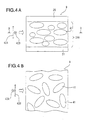
- FIGS. 4A and 4B schematically show the liquid crystal conditions at the non-display portion 24A (see FIG. 2) at the viewfinder display element 9, respectively in a sectional view and in a sectional view taken along B-B in FIG. 4A.
- the refractive-index isotropic material (monomer) and the refractive-index anisotropic material (liquid crystal) are present in an unhardened, mixed state.
- Reference numeral 41 indicates a liquid crystal molecule. The illuminating light enters from the left side in the figures.
- the liquid crystal molecules 41 in the liquid crystal sandwiched between the glass substrates 20 and 21 lie flat in layers. It is to be noted that since no orientation film is disposed at the viewfinder display element 9 in the embodiment, some of the liquid crystal molecules may not lie perfectly flat in layers and may instead be set at a slight tilt. However, they can be regarded to lie substantially flat in layers for practical purposes.
- the sectional view in FIG. 4B of the viewfinder display element 9 taken from above the substrate shows that the liquid crystal molecules 41 are oriented randomly (the optical axes of the liquid crystal molecules are arranged randomly).
- linearly polarized light indicated by reference numeral 42A enters through a side surface of the viewfinder display element 9 with the liquid crystal molecules 41 oriented as shown in FIGS. 4A and 4B. Since the liquid crystal molecules 41 lie flat, the refractive index at the liquid crystal and the refractive index at the monomer assume equal values with regard to linearly polarized light perpendicular to the substrates as the linearly polarized light 42A. Thus, the linearly polarized light 42A is transmitted through the non-display portion 24A without becoming scattered.
- the refractive index at the liquid crystal and the refractive index at the monomer assume values different from each other for the linearly polarized light 42B, inducing scattering of the linearly polarized light 42B over the non-display portion 24A.
- the polarizing plate 12 that allows polarized light perpendicular to the substrates to be transmitted is disposed between the light source 10 and the viewfinder display element 9 in the embodiment, as shown in FIGS. 1, 3A and 3B. Since the linearly polarized light 42A which is linearly polarized in a direction perpendicular to the substrates alone enters the viewfinder display element 9, the illuminating light is not scattered at the non-display portion 24A. As a result, the contrast between the display portions 30A through 30C and the non-display portion 24A around the display portions in FIG. 3A improves.
- the linearly polarized light 42A advances parallel to the direction in which the optical axes of the liquid crystal molecules extend when the voltage is applied to the transparent electrodes 22 and 23 in FIG. 2 and thus, the diffraction efficiency of the diffracted light exiting the viewfinder display element 9 can be improved, which, in turn, further improves the contrast.
- the linearly polarized illuminating light component is generated by using the light source 10 and the polarizing plate 12 in combination in the embodiment described above, the present invention is not limited to this example and various other illuminating means may be utilized, as long as similar illuminating light is generated.
- a selective polarization hologram may be used as the optical element that converts the illuminating light to the linearly polarized light 42A.
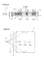
- FIGS. 5A and 5B present an example of a variation of the embodiment with FIG. 5A showing a viewfinder display element 9 in a sectional view taken from a side thereof and FIG. 5B showing the viewfinder display element in a plan view.
- the variation includes a hologram diffusion element 50 disposed between the polarizing plate 12 and the light source 10.
- Light from the light source 10 constituted with an LED is radiated over an angle range of approximately ⁇ 30 to 40°.
- the light having entered the viewfinder display element 9 undergoes total reflection at a side surface of the viewfinder display element 9.
- the side surface which assures total reflection is substantially perpendicular to the side surface of the viewfinder display element 9 to which illuminating light from the light source 10 enters.
- the illuminating light can be uniformly distributed over the entire range of the viewfinder display element 9, which enables uniform display via the display portions 30A through 30C.
- the optimal extent of diffusion (the extent of angle adjustment) via the hologram diffusion element 50 is achieved by taking into consideration the position at which the viewfinder display element 9 is disposed, the dimensions of the viewfinder display element 9, the total reflection angle and the like.
- an element other than a hologram diffusion element may be utilized as long as it is a radiation angle altering device capable of diffusing light by adjusting the illuminating light radiation angle.
- the diffraction display device may be mounted at various types of optical apparatus other than a camera.
- the display at the viewfinder display element 9 is turned on/off by turning on/off the voltage application to the transparent electrodes 22 and 23
- the present invention may also be adopted in a diffraction display device that does not include a transparent electrode. Namely, in the viewfinder display element 9 in FIG. 2 minus the transparent electrodes 22 and 23, the state of the orientation of the liquid crystal molecules in the refractive-index anisotropic area layers 242 is identical to the orientation state observed when the voltage application to the transparent electrodes 22 and 23 is turned off.
- the diffraction function works at all times in such a display element.
- the display via the display portion 24B is on.
- the ON/OFF state at the display portion 24B can be controlled by turning on/off the light source 10.
- the linearly polarized illuminating light enters the diffractive optical element through a side surface thereof, thereby reducing the extent of scattering of the illuminating light at the non-display portion and improving the contrast and the visibility.
Landscapes
- Physics & Mathematics (AREA)
- General Physics & Mathematics (AREA)
- Chemical & Material Sciences (AREA)
- Nonlinear Science (AREA)
- Dispersion Chemistry (AREA)
- Mathematical Physics (AREA)
- Crystallography & Structural Chemistry (AREA)
- Optics & Photonics (AREA)
- Liquid Crystal (AREA)
- Viewfinders (AREA)
- Diffracting Gratings Or Hologram Optical Elements (AREA)
- Indication In Cameras, And Counting Of Exposures (AREA)
Abstract
Description
- The present invention relates to a diffraction display device, a viewfinder display device and a camera.
-
Japanese Laid Open Patent Publication No. 2004-191415 - However, in the non-display portions around the display portion where the refractive index diffraction grating is formed so as to display characters or graphics, the material used to constitute the refractive-index isotropic areas and the material used to form the refractive-index anisotropic areas are present together in an unhardened mixed state. For this reason, the illuminating light having entered over this area becomes scattered, which then lowers the display contrast of the characters or the graphics on display, greatly compromising the functions of the optical display device.
- A diffraction display device according to a first aspect of the present invention includes a diffraction optical element that includes a diffraction display portion and a non-display portion disposed between a pair of substrates; and an illuminating device that emits linearly polarized illuminating light to be incident on a side surface of the diffraction optical element, wherein the illuminating light having entered the diffraction optical element exits the diffraction optical element through a substrate surface at which the diffraction display portion is disposed.
- It is preferable that the illuminating device includes a light source and a polarization conversion element that converts the light emitted from the light source to light that is linearly polarized in a direction perpendicular to the substrates. The polarization conversion element may be a selective polarization hologram element. A radiation angle altering device may be further provided, that is disposed between the light source and the polarization conversion element and alters a radiation angle of the illuminating light measured along a surface of the substrates.
- The radiation angle altering device may alter the radiation angle so as to ensure that the illuminating light having entered the diffraction optical element undergoes total reflection at a side surface of the diffraction optical element that is substantiallyperpendicular to the side surface to which the illuminating light enters. The light source may be a LED.
- It is preferable that the diffraction display portion includes refractive-index isotropic areas constituted with a refractive-index isotropic material and refractive-index anisotropic areas containing a refractive-index anisotropic liquid crystal disposed alternatively to each other in a direction extending along surfaces of the substrates; and the non-display portion is disposed around the diffraction display portion, and is constituted with a mixed material containing both the liquid crystal and the refractive-index isotropic material. In the diffraction display portion, the refractive-index isotropic areas may be constituted of a monomer that has hardened and become a polymer, and the liquid crystal may be dispersed in a hardened polymer in the refractive-index anisotropic areas.
- A view finder display device according to a second aspect of the present invention includes a diffraction display device according to the first aspect of the present invention, wherein the diffraction optical element is disposed in a vicinity of a focusing screen and viewfinder display is formed with the illuminating light diffracted at the diffraction display portion.
- A camera according to a third aspect of the present invention includes a viewfinder display device according to the second aspect of the present invention, wherein the viewfinder display device superimposes a predefined information over a photographed subject image.
- In a display method by using a diffraction optical element that comprises a diffraction display portion and a non-display portion disposed between a pair of substrates, according to a fourth aspect of the present invention, linearly polarized illuminating light is emitted to be incident on a side surface of the diffraction optical element, and the illuminating light having entered the diffraction optical element is diffracted so as the illuminating light to exit through a substrate surface at which the diffraction display portion is disposed.
-
- FIG. 1 schematically shows a structure of a single lens reflex camera equipped with a viewfinder display device according to an embodiment of the present invention;
- FIG. 2 is a schematic diagram of a viewfinder display element, illustrating a display portion and a non-display portion at the viewfinder display element;
- FIGS. 3A and 3B illustrate the voltage application OFF state and the voltage application ON state of the viewfinder display element;
- FIGS. 4A and 4B schematically illustrate part of the non-display portion of the viewfinder display element, respectively in a sectional view and in a sectional view taken along B-B in FIG. 4A;
- FIGS. 5A and 5B present an example of a variation of the embodiment with FIG. 5A showing a viewfinder display element in a sectional view and FIG. 5B showing the viewfinder display element in a plan view; and
- FIG. 6 presents a flowchart illustrating a displaymethod using the refractive index diffraction grating.
- The following is an explanation of an embodiment of the present invention, given in reference to the drawings. FIG. 1 schematically shows the structure of a single lens reflex camera equipped with a viewfinder display device achieved in the embodiment of the present invention. An
interchangeable lens barrel 3, which includes aphotographic lens 2, is mounted at acamera body 1. Reference numeral 4 indicates a film constituting a recording medium. While FIG. 1 shows a single lens reflex camera in which silver halide film is used, an imaging element such as a CCD or a CMOS should be used as the recording medium in a single lens reflex digital camera. - A quick-
return mirror 5 that reflects subject light toward a viewfinder optical system is disposed between thephotographic lens 2 and the film 4. It is to be noted that although not shown, a shutter is disposed between the film 4 and the quick-return mirror 5. Aviewfinder screen 6 is disposed at a position that is optically conjugate with the position of the surface of the film 4 coated with a photosensitive material, and an image is formed on theviewfinder screen 6 with the subject light from asubject 11 reflected at the quick-return mirror 5. The subject image formed on theviewfinder screen 6 can be observed via apentaprism 7 and aneyepiece lens 8. It is to be noted that the quick-return mirror 5 is made to assume a position outside the optical path of the subject light during a photographing operation so as to allow the subject image to be formed on the film 4. - In addition, a
viewfinder display element 9 is disposed inside thecamera body 1 at a position adjacent to theviewfinder screen 6. Alight source 10 that emits light used to illuminate theviewfinder display element 9 is disposed at a side of theviewfinder display element 9. Thelight source 10 may be constituted with an LED or the like. Thelight source 10 emits unpolarized light which includes naturally polarized light or partially polarized light. Between thelight source 10 and theviewfinder display element 9, a polarizingplate 12 constituting a polarization conversion element that converts the light from thelight source 10 to linearly polarized light is disposed. - The light emitted from the
light source 10 is converted to linearly polarized light at the polarizingplate 12 and enters theviewfinder display element 9 through a side surface thereof. As detailed later, theviewfinder display element 9 is a diffraction optical element that includes a display portion constituted with a refractive index diffraction grating, and the light having entered theviewfinder display element 9 is diffracted at the refractive index diffraction grating toward thepentaprism 7. Theviewfinder display element 9 is driven by adrive circuit 13, and specific information, e.g., a focal point detection area, exposure time, f-number, and the like, is displayed inside the viewfinder field via the display portion constituted with the refractive index diffraction grating. - The diffracted light having exited the
viewfinder display element 9 is reflected at thepentaprism 7 and is observed by an user as the specific information via theeyepiece lens 8. The specific information displayed or superimposed within the viewfinder field over the subject image mentioned earlier can be observed by the user together with the subject image. - Next, the
viewfinder display element 9 is explained in detail. FIG. 2 illustrates the display portion and the non-display portion of theviewfinder display element 9 in a schematic sectional view of theviewfinder display element 9. Theviewfinder display element 9 includes a pair ofglass substrate transparent electrodes glass substrates transparent electrodes transparent electrodes drive circuit 13 mentioned earlier and the voltage application to thetransparent electrodes drive circuit 13. - A
liquid crystal member 24 is disposed between theglass substrates transparent electrodes liquid crystal member 24 is sealed with aseal material 26 disposed over the peripheral areas between theglass substrates liquid crystal member 24 is constituted with a polymer-dispersed liquid crystal. Anon-display portion 24A where thetransparent electrodes - A
display portion 24B sandwiched between thetransparent electrodes isotropic area layers 241 and refractive-indexanisotropic area layers 242 alternating with each other in the illuminating light advancing direction along the plane of theviewfinder display element 9. The refractive-indexisotropic area layers 241 are constituted of the monomer mentioned earlier that has hardened and become a polymer whereas the refractive-index anisotropic material, i.e., the liquid crystal, is dispersed in the hardened polymer in the refractive-indexanisotropic area layers 242. - The multilayer structure in FIG. 2 is achieved by forming
interference fringes 25 with laser light or the like and then disposing a liquid crystal substrate constituted of a monomer and a liquid crystal in a mixed state over the area where theinterference fringes 25 are formed. At this time, masks are formed at theglass substrates interference fringes 25 are not formed over thenon-display portion 24A. As the monomer undergoes the process of photopolymerization and becomes hardened, polymer layers each constituted of the hardened monomer are formed overlight portions 251 in the interference fringes where the light intensity is high due to the interference. The speed of the photopolymerization overdark portions 252 in the interference fringes where the light intensity is not as high is lower than the photopolymerization speed at thelight portions 251 in the interference fringes, and thus, the monomer is drawn toward the areas with higher light intensity (the areas where the photopolymerization speed is higher), raising the liquid crystal density over thedark portions 252. As a result, the layered structure that includes the refractive-index isotropic area layers 241 constituted with the polymer and the refractive-index anisotropic area layers 242 constituted with the polymer with the high liquid crystal density is formed in a pattern identical to the pattern of theinterference fringes 25. - As described earlier, a voltage can be applied via the drive circuit 13 (see FIG. 1) to the
transparent electrodes display portion 24B. An isotropic refractive index is retained at the refractive-index isotropic area layers 241 constituted with the polymer, regardless of whether or not the voltage is applied. However, the orientation of the liquid crystal changes depending upon whether or not the voltage is applied at the refractive-index anisotropic area layers 242 where the liquid crystal is dispersed in the polymer, and as the liquid crystal orientation changes, the refractive index at the refractive-index anisotropic area layers 242, too, changes. - The refractive index at the liquid crystal and the refractive index at the polymer assume values different from each other so as to satisfy the Bragg diffraction condition with regard to light entering the
display element 9 toward the layering direction at thedisplay portion 24B, e.g., the illuminating light from thelight source 10, when the voltage is not applied to thetransparent electrodes display portion 24B. The diffraction conditions are set so that the diffracted light is diffracted toward thepentaprism 7 under these circumstances. As the voltage is applied, the orientation of the liquid crystal in the refractive-index anisotropic area layers 242 changes and the refractive index in the refractive-index anisotropic area layers 242, too, changes, so that the refractive index at the liquid crystal becomes equal to the refractive index at the polymer. Under these conditions, the light having entered thedisplay element 9 is transmitted through thedisplay portion 24B without becoming diffracted. - FIGS. 3A and 3B show the relationship between the ON/OFF state of the voltage applied to the transparent electrodes at the
viewfinder display element 9 and the display ON/OFF state. FIG. 3A shows the voltage application OFF state and FIG. 3B shows the voltage application ON state. It is to be noted that FIGS. 3A and 3B show threedisplay portions viewfinder display element 9, with theindividual display portions 30A through 30C each assuming a layered structure that includes refractive-index isotropic area layers and refractive-index anisotropic area layers, as does thedisplay portion 24B explained earlier. - As the voltage application to the transparent electrodes sandwiching the
display portions 30A through 30C is turned off, the portions assuming the layered structure described above function as a refractive index diffraction grating. The procedure of the display method by using such a refractive index diffraction grating is explained with reference to a flowchart shown in FIG. 6. Illuminating light from thelight source 10 having been converted to a linearly polarized light through thepolarizing plate 12 to be detailed later enters theviewfinder display element 9 through its side surface (step S1). - The illuminating light thus entered is diffracted at the
display portions viewfinder display element 9, as shown in FIG. 3A (step S2). As a result, the display pattern of thedisplay portions 30A through 30C superimposed over the subject image can be observed by the user. When the voltage application to the transparent electrodes is turned on, the illuminating light is not diffracted over the areas assuming the layered structure and is instead transmitted, as shown in FIG. 3B. Thus, the illuminating light is not guided to the eyepiece lens 8 (see FIG. 1) and the user is able to observe the subject image alone. - As described above, a structure in which the refractive index at the liquid crystal and the refractive index at the polymer are different from each other and the light is diffracted when no voltage is applied but the liquid crystal orientation becomes altered to set the refractive index at the liquid crystal substantially equal to that of the polymer when the voltage is applied, is adopted in the embodiment. However, the details of the liquid crystal orientation are not limited to this example, and instead, a structure in which the refractive index at the liquid crystal and the refractive index at the polymer are substantially equal to each other when the voltage is not applied and light becomes diffracted due to a difference between the refractive index at the liquid crystal and the refractive index at the polymer caused by a change in the liquid crystal orientation when the voltage is applied, may be adopted.
- In addition, while transparent electrodes assuming shapes substantially identical to each other are formed at the pair of
glass substrates glass substrates viewfinder display element 9 explained earlier. - Next, the functions of the
polarizing plate 12 are explained in reference to FIGS. 4A and 4B. FIGS. 4A and 4B schematically show the liquid crystal conditions at thenon-display portion 24A (see FIG. 2) at theviewfinder display element 9, respectively in a sectional view and in a sectional view taken along B-B in FIG. 4A. As explained earlier, over thenon-display portion 24A, the refractive-index isotropic material (monomer) and the refractive-index anisotropic material (liquid crystal) are present in an unhardened, mixed state.Reference numeral 41 indicates a liquid crystal molecule. The illuminating light enters from the left side in the figures. - When viewed from a lateral direction, as in the sectional view presented in FIG. 4A, the
liquid crystal molecules 41 in the liquid crystal sandwiched between theglass substrates viewfinder display element 9 in the embodiment, some of the liquid crystal molecules may not lie perfectly flat in layers and may instead be set at a slight tilt. However, they can be regarded to lie substantially flat in layers for practical purposes. The sectional view in FIG. 4B of theviewfinder display element 9 taken from above the substrate, on the other hand, shows that theliquid crystal molecules 41 are oriented randomly (the optical axes of the liquid crystal molecules are arranged randomly). - Let us now consider a situation in which linearly polarized light indicated by
reference numeral 42A enters through a side surface of theviewfinder display element 9 with theliquid crystal molecules 41 oriented as shown in FIGS. 4A and 4B. Since theliquid crystal molecules 41 lie flat, the refractive index at the liquid crystal and the refractive index at the monomer assume equal values with regard to linearly polarized light perpendicular to the substrates as the linearlypolarized light 42A. Thus, the linearlypolarized light 42A is transmitted through thenon-display portion 24A without becoming scattered. However, since theliquid crystal molecules 41 are oriented randomly with respect to linearlypolarized light 42B parallel to the substrates, the refractive index at the liquid crystal and the refractive index at the monomer assume values different from each other for the linearlypolarized light 42B, inducing scattering of the linearlypolarized light 42B over thenon-display portion 24A. - Accordingly, the
polarizing plate 12 that allows polarized light perpendicular to the substrates to be transmitted is disposed between thelight source 10 and theviewfinder display element 9 in the embodiment, as shown in FIGS. 1, 3A and 3B. Since the linearlypolarized light 42A which is linearly polarized in a direction perpendicular to the substrates alone enters theviewfinder display element 9, the illuminating light is not scattered at thenon-display portion 24A. As a result, the contrast between thedisplay portions 30A through 30C and thenon-display portion 24A around the display portions in FIG. 3A improves. - In addition, the linearly polarized light 42A advances parallel to the direction in which the optical axes of the liquid crystal molecules extend when the voltage is applied to the
transparent electrodes viewfinder display element 9 can be improved, which, in turn, further improves the contrast. It is to be noted that while the linearly polarized illuminating light component is generated by using thelight source 10 and thepolarizing plate 12 in combination in the embodiment described above, the present invention is not limited to this example and various other illuminating means may be utilized, as long as similar illuminating light is generated. For instance, instead of the absorptivepolarizing plate 12, a selective polarization hologram may be used as the optical element that converts the illuminating light to the linearlypolarized light 42A. - FIGS. 5A and 5B present an example of a variation of the embodiment with FIG. 5A showing a
viewfinder display element 9 in a sectional view taken from a side thereof and FIG. 5B showing the viewfinder display element in a plan view. The variation includes ahologram diffusion element 50 disposed between thepolarizing plate 12 and thelight source 10. Light from thelight source 10 constituted with an LED is radiated over an angle range of approximately ±30 to 40°. By adjusting the light beam angle to a greater value via thehologram diffusion element 50, the light having entered theviewfinder display element 9 undergoes total reflection at a side surface of theviewfinder display element 9. As shown in FIG. 5B, the side surface which assures total reflection is substantially perpendicular to the side surface of theviewfinder display element 9 to which illuminating light from thelight source 10 enters. - As a result, the illuminating light can be uniformly distributed over the entire range of the
viewfinder display element 9, which enables uniform display via thedisplay portions 30A through 30C. It is to be noted that the optimal extent of diffusion (the extent of angle adjustment) via thehologram diffusion element 50 is achieved by taking into consideration the position at which theviewfinder display element 9 is disposed, the dimensions of theviewfinder display element 9, the total reflection angle and the like. In addition, an element other than a hologram diffusion element may be utilized as long as it is a radiation angle altering device capable of diffusing light by adjusting the illuminating light radiation angle. - While an explanation is given above on an example in which the diffraction display device according to the embodiment of the present invention is used as a viewfinder display element in a camera, the diffraction display device may be mounted at various types of optical apparatus other than a camera. In addition, while the display at the
viewfinder display element 9 is turned on/off by turning on/off the voltage application to thetransparent electrodes viewfinder display element 9 in FIG. 2 minus thetransparent electrodes transparent electrodes light source 10 is in an ON state, the display via thedisplay portion 24B is on. In addition, the ON/OFF state at thedisplay portion 24B can be controlled by turning on/off thelight source 10. - By adopting the embodiments described above, the linearly polarized illuminating light enters the diffractive optical element through a side surface thereof, thereby reducing the extent of scattering of the illuminating light at the non-display portion and improving the contrast and the visibility.
- The above described embodiments are examples, and various modifications can be made without departing from the scope of the invention.
Claims (11)
- A diffraction display device comprising:a diffraction optical element (9) that comprises a diffraction display portion and a non-display portion disposed between a pair of substrates; andan illuminating device (10, 12) that emits linearly polarized illuminating light to be incident on a side surface of the diffraction optical element (9), wherein:the illuminating light having entered the diffraction optical element (9) exits the diffraction optical element (9) through a substrate surface at which the diffraction display portion is disposed.
- A diffraction display device according to claim 1,
wherein:the illuminating device (10, 12) comprises a light source (10) and a polarization conversion element (12) that converts the light emitted from the light source (10) to light that is linearly polarized in a direction perpendicular to the substrates. - A diffraction display device according to claim 2,
wherein:the polarization conversion element (12) is a selective polarization hologram element. - A diffraction display device according to claim 2 or claim 3, further comprising:a radiation angle altering device (50) that is disposed between the light source (10) and the polarization conversion element (12) and alters a radiation angle of the illuminating light measured along a surface of the substrates.
- A diffraction display device according to claim 4,
wherein:the radiation angle altering device (50) alters the radiation angle so as to ensure that the illuminating light having entered the diffraction optical element (9) undergoes total reflection at a side surface of the diffraction optical element (9) that is substantially perpendicular to the side surface to which the illuminating light enters. - A diffraction display device according to claim 4 or claim 5, wherein:the light source (10) is a LED.
- A diffraction display device according to any one of claims 1 through 6, wherein:the diffraction display portion comprises refractive-index isotropic areas constituted with a refractive-index isotropic material and refractive-index anisotropic areas containing a refractive-index anisotropic liquid crystal disposed alternatively to each other in a direction extending along surfaces of the substrates; andthe non-display portion is disposed around the diffraction display portion, and is constituted with a mixed material containing both the liquid crystal and the refractive-index isotropic material.
- A diffraction display device according to claim 7,
wherein:in the diffraction display portion, the refractive-index isotropic areas are constituted of a monomer that has hardened and become a polymer, and the liquid crystal is dispersed in a hardened polymer in the refractive-index anisotropic areas. - A viewfinder display device, comprising:a diffraction display device according to any one of claims 1 through 8, wherein:the diffraction optical element (9) is disposed in a vicinity of a focusing screen (6) and viewfinder display is formed with the illuminating light diffracted at the diffraction display portion.
- A camera, comprising:a viewfinder display device according to claim 9,wherein:the viewfinder display device superimposes a predefined information over a photographed subject image.
- A display method by using a diffraction optical element (9) that comprises a diffraction display portion and a non-display portion disposed between a pair of substrates, comprising:emitting linearly polarized illuminating light to be incident on a side surface of the diffraction optical element (9), anddiffracting the illuminating light having entered the diffraction optical element (9) so as the illuminating light to exit through a substrate surface at which the diffraction display portion is disposed.
Applications Claiming Priority (1)
| Application Number | Priority Date | Filing Date | Title |
|---|---|---|---|
| JP2005150027A JP4586630B2 (en) | 2005-05-23 | 2005-05-23 | Diffraction type display device and display device in viewfinder of camera |
Publications (2)
| Publication Number | Publication Date |
|---|---|
| EP1726986A1 true EP1726986A1 (en) | 2006-11-29 |
| EP1726986B1 EP1726986B1 (en) | 2010-07-21 |
Family
ID=36763692
Family Applications (1)
| Application Number | Title | Priority Date | Filing Date |
|---|---|---|---|
| EP06114124A Ceased EP1726986B1 (en) | 2005-05-23 | 2006-05-17 | Diffractive display device and corresponding display method |
Country Status (5)
| Country | Link |
|---|---|
| US (1) | US7542669B2 (en) |
| EP (1) | EP1726986B1 (en) |
| JP (1) | JP4586630B2 (en) |
| CN (1) | CN1892338B (en) |
| DE (1) | DE602006015566D1 (en) |
Families Citing this family (15)
| Publication number | Priority date | Publication date | Assignee | Title |
|---|---|---|---|---|
| JP5309468B2 (en) | 2006-05-31 | 2013-10-09 | 株式会社ニコン | Liquid crystal display element, display device, observation device, and camera |
| JP2008015125A (en) * | 2006-07-05 | 2008-01-24 | Nikon Corp | Display element, display device, and camera |
| WO2008044648A1 (en) * | 2006-10-06 | 2008-04-17 | Nikon Corporation | Diffractive display device, finder device and camera |
| WO2008105395A1 (en) * | 2007-02-26 | 2008-09-04 | Nikon Corporation | Display device, finder device, and camera |
| WO2009069249A1 (en) * | 2007-11-30 | 2009-06-04 | Sharp Kabushiki Kaisha | Liquid crystal display |
| JP2011059582A (en) * | 2009-09-14 | 2011-03-24 | Sony Corp | Imaging device |
| GB201015417D0 (en) * | 2010-09-15 | 2010-10-27 | Lomox Ltd | Organic light emitting diode devices |
| WO2014167308A1 (en) * | 2013-04-10 | 2014-10-16 | Bae Systems Plc | Spectral imaging |
| US10324245B2 (en) | 2014-07-29 | 2019-06-18 | Samsung Electronics Co., Ltd. | Backlight unit for holographic display |
| US11126060B2 (en) | 2017-10-02 | 2021-09-21 | Liqxtal Technology Inc. | Tunable light projector |
| US20190101791A1 (en) * | 2017-10-02 | 2019-04-04 | Liqxtal Technology Inc. | Optical sensing device and structured light projector |
| US10969668B2 (en) * | 2018-07-24 | 2021-04-06 | Qualcomm Incorporated | Adjustable light distribution for active depth sensing systems |
| KR102707258B1 (en) * | 2018-10-15 | 2024-09-23 | 삼성디스플레이 주식회사 | Display device and fabricating method thereof |
| KR102791249B1 (en) * | 2019-07-09 | 2025-04-08 | 현대자동차주식회사 | Transparency variable glass and apparatus of controlling transparency of the same |
| CN113272726B (en) * | 2019-10-24 | 2022-08-23 | 京东方科技集团股份有限公司 | Display panel, display device and display panel manufacturing method |
Citations (2)
| Publication number | Priority date | Publication date | Assignee | Title |
|---|---|---|---|---|
| EP1213601A1 (en) * | 1999-06-23 | 2002-06-12 | Citizen Watch Co. Ltd. | Liquid crystal display |
| WO2004053575A1 (en) * | 2002-12-06 | 2004-06-24 | Nikon Corporation | Holographic optical device, camera finder indication, and camera |
Family Cites Families (6)
| Publication number | Priority date | Publication date | Assignee | Title |
|---|---|---|---|---|
| JPH09152553A (en) | 1995-11-30 | 1997-06-10 | Mitsubishi Electric Corp | Light source device and projection display device using the same |
| EP1281022A1 (en) * | 2000-05-04 | 2003-02-05 | Koninklijke Philips Electronics N.V. | Illumination unit for a device having a multi-color reflective liquid crystal display |
| JP2002023107A (en) * | 2000-07-05 | 2002-01-23 | Sony Corp | Image display device and image display device |
| JP2002122906A (en) * | 2000-10-17 | 2002-04-26 | Olympus Optical Co Ltd | Display device in viewfinder |
| JP2002221621A (en) * | 2001-01-26 | 2002-08-09 | Sony Corp | Polarization selective hologram optical element, image display element and image display device |
| WO2003019247A1 (en) * | 2001-08-24 | 2003-03-06 | Asahi Glass Company, Limited | Multi-layer diffraction type polarizer and liquid crystal element |
-
2005
- 2005-05-23 JP JP2005150027A patent/JP4586630B2/en not_active Expired - Fee Related
-
2006
- 2006-05-17 EP EP06114124A patent/EP1726986B1/en not_active Ceased
- 2006-05-17 DE DE602006015566T patent/DE602006015566D1/en not_active Expired - Lifetime
- 2006-05-19 US US11/436,611 patent/US7542669B2/en not_active Expired - Fee Related
- 2006-05-23 CN CN2006100848552A patent/CN1892338B/en not_active Expired - Fee Related
Patent Citations (3)
| Publication number | Priority date | Publication date | Assignee | Title |
|---|---|---|---|---|
| EP1213601A1 (en) * | 1999-06-23 | 2002-06-12 | Citizen Watch Co. Ltd. | Liquid crystal display |
| WO2004053575A1 (en) * | 2002-12-06 | 2004-06-24 | Nikon Corporation | Holographic optical device, camera finder indication, and camera |
| US20060034603A1 (en) * | 2002-12-06 | 2006-02-16 | Nikon Corporation | Holographic optical device, camera finder indication, and camera |
Non-Patent Citations (1)
| Title |
|---|
| DATE MUNEKAZU ET AL: "Diffraction-controlling display with edge lighting using alignment-controlled holographic polymer dispersed liquid crystal (AC-HPDLC)", SID CONF REC INT DISPLAY RES CONF; SID CONFERENCE RECORD OF THE INTERNATIONAL DISPLAY RESEARCH CONFERENCE 2001, 16 October 2001 (2001-10-16) - 19 October 2001 (2001-10-19), pages 297 - 300, XP009071069 * |
Also Published As
| Publication number | Publication date |
|---|---|
| US7542669B2 (en) | 2009-06-02 |
| CN1892338B (en) | 2011-11-09 |
| JP4586630B2 (en) | 2010-11-24 |
| JP2006330103A (en) | 2006-12-07 |
| US20060263079A1 (en) | 2006-11-23 |
| EP1726986B1 (en) | 2010-07-21 |
| CN1892338A (en) | 2007-01-10 |
| DE602006015566D1 (en) | 2010-09-02 |
Similar Documents
| Publication | Publication Date | Title |
|---|---|---|
| EP1726986B1 (en) | Diffractive display device and corresponding display method | |
| JP4631308B2 (en) | Image display device | |
| JP2008015125A (en) | Display element, display device, and camera | |
| US8345189B2 (en) | Diffractive display device, finder device and camera | |
| JP3852799B2 (en) | Illumination light guide plate for reflective LCD | |
| US6975810B2 (en) | Focal point detection device and camera | |
| US20070274701A1 (en) | Transparent display and camera | |
| WO2004053575A1 (en) | Holographic optical device, camera finder indication, and camera | |
| US7652710B2 (en) | Camera with photometric function and optical element for camera | |
| JP5218392B2 (en) | Display device, finder device and camera | |
| US7702237B2 (en) | Observation device, camera and observation method | |
| JP4788301B2 (en) | Display device and camera | |
| JP2007047769A (en) | Display device | |
| JP5169420B2 (en) | Lighting device, display device, finder device, and camera | |
| JP3608391B2 (en) | Holographic diffusion sheet and reflective liquid crystal display device using the same | |
| JP4544207B2 (en) | Display device and camera | |
| JP2007017695A (en) | Display device and camera | |
| JP2007047578A (en) | Diffractive optical device and camera | |
| US7796181B2 (en) | Color temperature conversion element, color temperature conversion device and illuminator | |
| JP2008203325A (en) | Display device, viewfinder device, camera, and display device manufacturing method | |
| JP2007017788A (en) | Display device | |
| JP2008227868A (en) | Display device, finder device and camera | |
| JP5169417B2 (en) | Lighting device, display device, finder device, and camera | |
| JPH0915684A (en) | Viewfinder | |
| JPS63218920A (en) | Light modulation element and observation device and projection display device using the same |
Legal Events
| Date | Code | Title | Description |
|---|---|---|---|
| PUAI | Public reference made under article 153(3) epc to a published international application that has entered the european phase |
Free format text: ORIGINAL CODE: 0009012 |
|
| AK | Designated contracting states |
Kind code of ref document: A1 Designated state(s): AT BE BG CH CY CZ DE DK EE ES FI FR GB GR HU IE IS IT LI LT LU LV MC NL PL PT RO SE SI SK TR |
|
| AX | Request for extension of the european patent |
Extension state: AL BA HR MK YU |
|
| 17P | Request for examination filed |
Effective date: 20070412 |
|
| AKX | Designation fees paid |
Designated state(s): DE FR GB |
|
| RTI1 | Title (correction) |
Free format text: DIFFRACTIVE DISPLAY DEVICE AND CORRESPONDING DISPLAY METHOD |
|
| GRAP | Despatch of communication of intention to grant a patent |
Free format text: ORIGINAL CODE: EPIDOSNIGR1 |
|
| GRAS | Grant fee paid |
Free format text: ORIGINAL CODE: EPIDOSNIGR3 |
|
| GRAA | (expected) grant |
Free format text: ORIGINAL CODE: 0009210 |
|
| AK | Designated contracting states |
Kind code of ref document: B1 Designated state(s): DE FR GB |
|
| REG | Reference to a national code |
Ref country code: GB Ref legal event code: FG4D |
|
| RAP2 | Party data changed (patent owner data changed or rights of a patent transferred) |
Owner name: NIKON CORPORATION |
|
| REF | Corresponds to: |
Ref document number: 602006015566 Country of ref document: DE Date of ref document: 20100902 Kind code of ref document: P |
|
| PLBE | No opposition filed within time limit |
Free format text: ORIGINAL CODE: 0009261 |
|
| STAA | Information on the status of an ep patent application or granted ep patent |
Free format text: STATUS: NO OPPOSITION FILED WITHIN TIME LIMIT |
|
| 26N | No opposition filed |
Effective date: 20110426 |
|
| REG | Reference to a national code |
Ref country code: DE Ref legal event code: R097 Ref document number: 602006015566 Country of ref document: DE Effective date: 20110426 |
|
| REG | Reference to a national code |
Ref country code: FR Ref legal event code: PLFP Year of fee payment: 11 |
|
| REG | Reference to a national code |
Ref country code: FR Ref legal event code: PLFP Year of fee payment: 12 |
|
| REG | Reference to a national code |
Ref country code: FR Ref legal event code: PLFP Year of fee payment: 13 |
|
| PGFP | Annual fee paid to national office [announced via postgrant information from national office to epo] |
Ref country code: DE Payment date: 20190508 Year of fee payment: 14 |
|
| PGFP | Annual fee paid to national office [announced via postgrant information from national office to epo] |
Ref country code: GB Payment date: 20190515 Year of fee payment: 14 |
|
| PGFP | Annual fee paid to national office [announced via postgrant information from national office to epo] |
Ref country code: FR Payment date: 20200414 Year of fee payment: 15 |
|
| REG | Reference to a national code |
Ref country code: DE Ref legal event code: R119 Ref document number: 602006015566 Country of ref document: DE |
|
| GBPC | Gb: european patent ceased through non-payment of renewal fee |
Effective date: 20200517 |
|
| PG25 | Lapsed in a contracting state [announced via postgrant information from national office to epo] |
Ref country code: GB Free format text: LAPSE BECAUSE OF NON-PAYMENT OF DUE FEES Effective date: 20200517 |
|
| PG25 | Lapsed in a contracting state [announced via postgrant information from national office to epo] |
Ref country code: DE Free format text: LAPSE BECAUSE OF NON-PAYMENT OF DUE FEES Effective date: 20201201 |
|
| PG25 | Lapsed in a contracting state [announced via postgrant information from national office to epo] |
Ref country code: FR Free format text: LAPSE BECAUSE OF NON-PAYMENT OF DUE FEES Effective date: 20210531 |