EP1720205A2 - Trench transistor DRAM cell array and method of making the same - Google Patents
Trench transistor DRAM cell array and method of making the same Download PDFInfo
- Publication number
- EP1720205A2 EP1720205A2 EP06008676A EP06008676A EP1720205A2 EP 1720205 A2 EP1720205 A2 EP 1720205A2 EP 06008676 A EP06008676 A EP 06008676A EP 06008676 A EP06008676 A EP 06008676A EP 1720205 A2 EP1720205 A2 EP 1720205A2
- Authority
- EP
- European Patent Office
- Prior art keywords
- source
- memory cell
- cell array
- drain regions
- openings
- Prior art date
- Legal status (The legal status is an assumption and is not a legal conclusion. Google has not performed a legal analysis and makes no representation as to the accuracy of the status listed.)
- Withdrawn
Links
- 238000004519 manufacturing process Methods 0.000 title claims description 7
- 239000000758 substrate Substances 0.000 claims abstract description 64
- 239000003990 capacitor Substances 0.000 claims abstract description 43
- 238000002955 isolation Methods 0.000 claims abstract description 41
- 239000004065 semiconductor Substances 0.000 claims abstract description 19
- 238000003860 storage Methods 0.000 claims abstract description 19
- VYPSYNLAJGMNEJ-UHFFFAOYSA-N Silicium dioxide Chemical compound O=[Si]=O VYPSYNLAJGMNEJ-UHFFFAOYSA-N 0.000 claims description 87
- 239000000377 silicon dioxide Substances 0.000 claims description 44
- 235000012239 silicon dioxide Nutrition 0.000 claims description 36
- 238000000034 method Methods 0.000 claims description 29
- 238000005530 etching Methods 0.000 claims description 25
- 125000006850 spacer group Chemical group 0.000 claims description 21
- 239000011810 insulating material Substances 0.000 claims description 17
- 238000005468 ion implantation Methods 0.000 claims description 16
- 239000004020 conductor Substances 0.000 claims description 15
- 239000000463 material Substances 0.000 claims description 15
- 238000000151 deposition Methods 0.000 claims description 8
- 150000002500 ions Chemical class 0.000 claims description 5
- 238000000059 patterning Methods 0.000 claims description 2
- 229910052581 Si3N4 Inorganic materials 0.000 description 23
- HQVNEWCFYHHQES-UHFFFAOYSA-N silicon nitride Chemical compound N12[Si]34N5[Si]62N3[Si]51N64 HQVNEWCFYHHQES-UHFFFAOYSA-N 0.000 description 21
- XUIMIQQOPSSXEZ-UHFFFAOYSA-N Silicon Chemical compound [Si] XUIMIQQOPSSXEZ-UHFFFAOYSA-N 0.000 description 13
- 229910052710 silicon Inorganic materials 0.000 description 13
- 239000010703 silicon Substances 0.000 description 13
- 239000005380 borophosphosilicate glass Substances 0.000 description 12
- 238000003491 array Methods 0.000 description 6
- 238000002513 implantation Methods 0.000 description 5
- 229910021420 polycrystalline silicon Inorganic materials 0.000 description 5
- 230000008569 process Effects 0.000 description 4
- 230000008901 benefit Effects 0.000 description 3
- KRHYYFGTRYWZRS-UHFFFAOYSA-N Fluorane Chemical compound F KRHYYFGTRYWZRS-UHFFFAOYSA-N 0.000 description 2
- 230000004888 barrier function Effects 0.000 description 2
- 238000004140 cleaning Methods 0.000 description 2
- 238000009792 diffusion process Methods 0.000 description 2
- 238000001312 dry etching Methods 0.000 description 2
- 230000001965 increasing effect Effects 0.000 description 2
- 230000004048 modification Effects 0.000 description 2
- 238000012986 modification Methods 0.000 description 2
- VHUUQVKOLVNVRT-UHFFFAOYSA-N Ammonium hydroxide Chemical compound [NH4+].[OH-] VHUUQVKOLVNVRT-UHFFFAOYSA-N 0.000 description 1
- ZOXJGFHDIHLPTG-UHFFFAOYSA-N Boron Chemical group [B] ZOXJGFHDIHLPTG-UHFFFAOYSA-N 0.000 description 1
- 230000003213 activating effect Effects 0.000 description 1
- 238000000137 annealing Methods 0.000 description 1
- 238000010276 construction Methods 0.000 description 1
- 230000008878 coupling Effects 0.000 description 1
- 238000010168 coupling process Methods 0.000 description 1
- 238000005859 coupling reaction Methods 0.000 description 1
- 230000003247 decreasing effect Effects 0.000 description 1
- 230000001419 dependent effect Effects 0.000 description 1
- 238000010586 diagram Methods 0.000 description 1
- 238000009826 distribution Methods 0.000 description 1
- 239000002019 doping agent Substances 0.000 description 1
- 230000009977 dual effect Effects 0.000 description 1
- 230000005684 electric field Effects 0.000 description 1
- 238000005516 engineering process Methods 0.000 description 1
- 230000002708 enhancing effect Effects 0.000 description 1
- 239000007943 implant Substances 0.000 description 1
- 238000011065 in-situ storage Methods 0.000 description 1
- 238000009413 insulation Methods 0.000 description 1
- 230000003993 interaction Effects 0.000 description 1
- 238000010849 ion bombardment Methods 0.000 description 1
- 230000014759 maintenance of location Effects 0.000 description 1
- 230000035515 penetration Effects 0.000 description 1
- 230000002093 peripheral effect Effects 0.000 description 1
- 238000005498 polishing Methods 0.000 description 1
- 229920005591 polysilicon Polymers 0.000 description 1
- 229910052814 silicon oxide Inorganic materials 0.000 description 1
- 239000002210 silicon-based material Substances 0.000 description 1
- 239000000126 substance Substances 0.000 description 1
- 238000012876 topography Methods 0.000 description 1
- 238000001039 wet etching Methods 0.000 description 1
Images







Classifications
-
- H—ELECTRICITY
- H10—SEMICONDUCTOR DEVICES; ELECTRIC SOLID-STATE DEVICES NOT OTHERWISE PROVIDED FOR
- H10B—ELECTRONIC MEMORY DEVICES
- H10B12/00—Dynamic random access memory [DRAM] devices
- H10B12/01—Manufacture or treatment
- H10B12/02—Manufacture or treatment for one transistor one-capacitor [1T-1C] memory cells
- H10B12/05—Making the transistor
- H10B12/053—Making the transistor the transistor being at least partially in a trench in the substrate
-
- H—ELECTRICITY
- H10—SEMICONDUCTOR DEVICES; ELECTRIC SOLID-STATE DEVICES NOT OTHERWISE PROVIDED FOR
- H10B—ELECTRONIC MEMORY DEVICES
- H10B12/00—Dynamic random access memory [DRAM] devices
- H10B12/30—DRAM devices comprising one-transistor - one-capacitor [1T-1C] memory cells
- H10B12/34—DRAM devices comprising one-transistor - one-capacitor [1T-1C] memory cells the transistor being at least partially in a trench in the substrate
-
- H—ELECTRICITY
- H10—SEMICONDUCTOR DEVICES; ELECTRIC SOLID-STATE DEVICES NOT OTHERWISE PROVIDED FOR
- H10B—ELECTRONIC MEMORY DEVICES
- H10B12/00—Dynamic random access memory [DRAM] devices
- H10B12/30—DRAM devices comprising one-transistor - one-capacitor [1T-1C] memory cells
- H10B12/48—Data lines or contacts therefor
- H10B12/488—Word lines
-
- H—ELECTRICITY
- H10—SEMICONDUCTOR DEVICES; ELECTRIC SOLID-STATE DEVICES NOT OTHERWISE PROVIDED FOR
- H10B—ELECTRONIC MEMORY DEVICES
- H10B12/00—Dynamic random access memory [DRAM] devices
- H10B12/30—DRAM devices comprising one-transistor - one-capacitor [1T-1C] memory cells
- H10B12/31—DRAM devices comprising one-transistor - one-capacitor [1T-1C] memory cells having a storage electrode stacked over the transistor
- H10B12/315—DRAM devices comprising one-transistor - one-capacitor [1T-1C] memory cells having a storage electrode stacked over the transistor with the capacitor higher than a bit line
-
- H—ELECTRICITY
- H10—SEMICONDUCTOR DEVICES; ELECTRIC SOLID-STATE DEVICES NOT OTHERWISE PROVIDED FOR
- H10D—INORGANIC ELECTRIC SEMICONDUCTOR DEVICES
- H10D89/00—Aspects of integrated devices not covered by groups H10D84/00 - H10D88/00
- H10D89/10—Integrated device layouts
Definitions
- the present invention relates to a memory cell array as well as to a method of manufacturing a memory cell array.
- Memory cells of a dynamic random access memory generally comprise a storage capacitor for storing an electrical charge which represents an information to be stored, and an access transistor connected with the storage capacitor.
- the access transistor comprises a first and a second source/drain regions, a channel connecting the first and second source/drain regions as well as a gate electrode controlling an electrical current flowing between the first and second source/drain regions.
- the transistor usually is at least partially formed in a semiconductor substrate.
- the information stored in the storage capacitor is read out or written in by addressing the access transistor via the corresponding word line. In particular, the information is read out to a corresponding bit line via a bit line contact.
- the lower boundary of the effective channel length L eff limits the scalability of planar transistor cells having an access transistor which is horizontally formed with respect to the substrate surface of the semiconductor substrate.
- Vertical transistor cells offer a possibility of enhancing the channel length while maintaining the surface area necessary for forming the memory cell.
- the source/drain regions of the access transistor as well as the channel region are arranged in a direction perpendicular to the substrate surface.
- One of the problems involved with such a vertical transistor cell is the difficulty in providing a surface contact to a stacked capacitor. Accordingly, such a vertical transistor is difficult to integrate with a stacked capacitor.
- a concept, in which the effective channel length L eff is enhanced, refers to a recessed channel transistor, as is for example known from US Patent No. 5,945,707 the disclosure of which is incorporated herein by reference in its entirety.
- the first and second source/drain regions are arranged in a horizontal plane parallel to the substrate surface.
- the gate electrode is arranged in a recess groove, which is disposed between the two source/drain regions of the transistor in the semiconductor substrate. Accordingly, the effective channel length equals to the sum of the distance between the two source/drain regions and the two fold of the depth of the recess groove.
- the effective channel width W eff corresponds to the nominal structural size F.
- U.S. Patent No. 5,502,320 discloses a memory cell array in which transistors are formed in continuous active area lines. The active area lines are arranged in parallel with the bit lines.
- the gate electrodes of the transistors from part from the word lines and the word lines including the gate electrodes are implemented as buried word lines.
- DE 103 61 695 B3 discloses a transistor which is formed in an active area having the form of a ridge, wherein two gate electrodes each forming part of a corresponding word lines are disposed along the lateral sides of the active area.
- the active area is recessed at a channel portion of the transistor.
- the above object is achieved by the memory cell array of claim 1. Moreover, the object is achieved by the method of forming a memory cell array as defined in claim 14.
- the preferred embodiments of the present invention are set forth in the dependent claims.
- the present invention provides a memory cell array comprising a plurality of memory cells, the memory cell array comprising a plurality of active areas being formed in a semiconductor substrate having a substrate surface, each of said active areas having two lateral sides extending along a first direction, rows of said active areas being separated from each other by isolation grooves extending along said first direction, each of said memory cells comprising a storage capacitor, a transistor which is at least partially formed in one of said active areas, said transistor comprising a first source/drain region which is connected with an electrode of said storage capacitor, said first source/drain region being formed adjacent to said substrate surface, a second source/drain region being formed adjacent to said substrate surface, a channel region connecting said first and second source/drain regions, said channel region being disposed in said active area, said channel region extending along said first direction, and a gate electrode disposed along said channel region and being electrically isolated from said channel region by a gate insulating layer, said gate electrode controlling an electrical current flowing between said first and second source/drain regions, wherein
- the word lines including the gate electrodes form a kind of a ladder structure according to which two word lines of the memory cell array are arranged in parallel with the channel.
- the channel is crossed by a gate electrode which connects the two word lines.
- two word lines can be disposed in each of said isolation grooves, the two word lines being insulated from each other and being assigned to two different rows of active areas.
- the word lines can easily be formed by a spacer process without the necessity of performing lithographic steps.
- the exact positioning of the word lines is ensured since the step of forming the word lines is performed self-aligned with respect to the isolation grooves and, consequently, the active areas.
- each of the gate electrode has a top side, said top side of said gate electrode being disposed beneath said surface of said semiconductor substrate.
- the channel connecting first and second source/drain regions is implemented as a curved or recessed channel.
- the active area has the shape of a "U", wherein the first and second source/drain regions are disposed in the vertical portions of the active area.
- the ladder structure of the word lines including the gate electrodes is supported by the vertical portion of the active areas in which the first and second source/drain regions are formed.
- the active area has the shape of a "U" and the channel is a curved or recessed channel, a distance between the doped source/drain regions can be enlarged without increasing the area of the transistor. Due to the enlarged distance, an electrical field at the source/drain region - channel junction and, hence, a leakage current is decreased.
- the special structure of two adjacent word lines and the corresponding gate electrodes, by which structure a ladder is formed can be implemented with any arbitrary shape of the active area.
- the channel region comprises a fin-region in which the channel has the shape of a ridge, said ridge comprising a top side and two lateral sides in a cross section perpendicular to a line connecting said first and second source/drain regions, and wherein said gate electrode is disposed at three sides of said ridge.
- the effective width of the channel is enlarged improving the characteristics of the transistor.
- the transistor of the memory cell array of the present invention provides an improved on-current in comparison with known transistors, since the width of the channel is increased whereby the resistance is reduced. Nevertheless, due to the narrow width of the fin region, the transistor body can be fully depleted, so that the off-current of the transistor can be improved.
- the special structure of two adjacent word lines and the corresponding gate electrodes, by which structure a ladder is formed can be implemented with any arbitrary shape of the channel region.
- the storage capacitor can be implemented as a stacked capacitor.
- the plurality of memory cells are arranged in rows and columns, respectively, two adjacent rows of memory cells being separated by two word lines that are electrically isolated from each other, wherein the memory cells are arranged in the form of a regular grid.
- the memory cells of adjacent rows are disposed in the same columns, respectively.
- the memory cells of adjacent columns are disposed in the same rows, respectively.
- the gate electrode has a bottom side, each of said first and second source/drain regions extending to a depth below or equal to said bottom side of said gate electrode.
- bit lines are formed on the substrate surface.
- bit lines are directly adjacent to the substrate surface so that the bit lines are connected with the second source/drain regions without the necessity of a bit line contact.
- an insulating spacer is disposed between said first source/drain region and said gate electrode and between said second source/drain region and said gate electrode, said insulating spacer having a larger thickness than said gate insulating layer.
- the influence of the potential of the gate electrode on the first and second source/drain regions can be lowered.
- the retention time of the memory cell i.e. the time during which an information can be recognizably stored in the memory cell, can be improved.
- the thickness of the gate insulating layer is smaller than that of the insulating spacer, the conductivity of the channel can be effectively controlled.
- the spacer is made of silicon dioxide, the influence of the gate electrode on the first and second source/drain regions can further be lowered.
- the present invention further provides a method of manufacturing a memory cell array comprising the steps of providing a semiconductor substrate having a substrate surface, forming first and second openings in said substrate surface, said first openings having a larger depth than said second openings, said depth being measured from said substrate surface, two first openings being followed by one second opening, and one second opening being followed by two first openings, defining isolation trenches in said semiconductor substrate, active areas being formed between two adjacent isolation trenches, filling said isolation trenches with an insulating material, providing a gate insulating layer on a bottom side of said second openings, providing a conductive material in said second openings and on the side walls of said isolation trenches, gate electrodes being formed of the conductive material in said second openings and word lines being formed of the conductive material on the side walls of said isolation trenches, providing an insulating material on the top side of said gate electrodes and between the word lines of one isolation trench, providing first and second source/drain regions in said substrate material between said first and second openings in an active area
- the gate electrodes are defined.
- the vertical portions of the active areas in which the first and second source/drain portions are to be formed are defined.
- the isolation trenches are formed after defining the vertical portions of the active areas in which the first and second source/drain portions are to be formed. As a consequence, the isolation trenches are formed in a self-aligned manner with respect to the first and second source/drain portions.
- said first and second openings are defined using a hardmask comprising first, second and third stripes of a first, a second, and a third material, respectively, the first, second and third stripes being arranged parallel to each other, and each of the first, second and third material being able to be etched selectively to each other.
- the depth of the first openings is equal to the depth of said isolation trenches, said depth being measured from said substrate surface.
- the first and second source/drain regions are not masked, whereas all the remaining portions of the surface are covered by an insulating material.
- bit lines so as to be in contact with the second source/drain regions of the transistors in a self-aligned manner.
- the step of forming the plurality of bit lines preferably comprises the steps of depositing at least one layer of a conductive material and patterning said at least one layer so as to form bit lines which are in contact with the second source/drain regions of the transistors.
- At least one layer is photolithographically patterned using a mask having a lines/spaces pattern.
- a mask having a lines/spaces pattern is easier to handle and to position.
- the step of providing a conductive material preferably comprises the steps of conformally depositing said conductive material and anisotropically etching said conductive material.
- the method of the invention further comprises the step of providing a first and a second lightly doped portions, said step being performed after the step of filling said isolation trenches with an insulating material, comprising the steps of providing an insulating material in said second opening, conducting an angled ion implantation step at an angle ⁇ between said substrate surface and a direction of said ions.
- the steps of providing an insulating material in said second opening conducting an angled ion implantation step at an angle ⁇ between said substrate surface and a direction of said ions.
- the method of the invention preferably comprises the step of removing the upper part of said insulating material from said isolation trenches so as to expose the upper part of said active area before providing said gate insulating layer, said gate insulating layer being formed on the exposed portions of said active area.
- a FINFET in which the channel has the shape of a ridge can easily be formed.
- the step of providing first and second source/drain regions preferably comprises the step of providing a first and a second lightly doped portions, said step being performed after the step of providing an insulating material on the top side of said gate electrodes and between the word lines of one isolation trench, the step of providing a first and a second lightly doped portions being performed by conducting an angled ion implantation step at an angle ⁇ between said substrate surface and a direction of said ions.
- the doping profile of the doped portions can be arbitrarily adjusted.
- the depth and the distribution of the dopants in the active areas can be adjusted.
- a silicon dioxide (SiO 2 ) layer 20 having a thickness of 70 to 100 nm is deposited as a first hard mask layer.
- the SiO 2 layer 20 is photolithographically patterned using a mask having a lines/spacers pattern.
- the lithographic mask used has a pattern having a line width of 1,4 F and a space width of 1,2 F.
- F denotes the minimum line width of the feature size which can be obtained by the technology used.
- F can be less than 100 nm and, in particular, 90, 70 or even 40 nm.
- a silicon nitride (Si 3 N 4 ) layer 21 is conformally deposited by generally known methods.
- the Si 3 N 4 layer 21 can have a thickness of approximately 0,3 F.
- an anisotropic etching step is performed so as to expose the horizontal portions of the silicon dioxide layer 20 and the silicon substrate 1.
- the sidewalls of the spaces of the SiO 2 layer 20 are covered by Si 3 N 4 spacers 21.
- a nitridation step as is generally known is performed so as to provide a diffusion barrier.
- a thin Si 3 N 4 layer is formed, for example, by exposing the substrate to a NH 3 atmosphere. This thin Si 3 N 4 layer prevents boron atoms from outdiffusing from the BPSG layer which is to be formed in the next step.
- a BPSG layer is deposited by generally known methods, an annealing step is performed and thereafter a CMP step is conducted so that finally the structure shown in Fig. 1A is obtained.
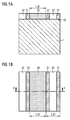
- Fig. 1A shows a cross-sectional view of the resulting structure.
- a semiconductor substrate 1 such as a silicon substrate
- a stripe of a silicon dioxide layer 20 having a width of 1,4 F is formed on the surface 10 of a semiconductor substrate 1, such as a silicon substrate.
- a stripe of a silicon dioxide layer 20 having a width of 1,4 F is formed on both sides of the silicon dioxide layer 20.
- stripes 21 of a silicon nitride layer 21 are arranged, followed by stripes of a BPSG layer 22.
- the width of the silicon nitride stripes 21 is approximately 0,3 F
- the width of the stripes 22 of the BPSG layer is approximately 0,6 F.
- Fig. 1B shows a plan view of the resulting structure. As can be seen, the whole surface 10 of the semiconductor substrate 1 is covered by stripes of a silicon dioxide layer 20, parallel stripes 21 of a silicon nitride layer and parallel stripes 22 of a BPSG layer. As is to be noted from Fig. 1B, the cross-sectional view of Fig. 1A is taken between I and I in Fig. 1B.
- the stripes of the BPSG layer 22 are etched selectively with respect to silicon dioxide.
- an etching step in HF vapour can be used for etching the BPSG layer.
- the silicon substrate is etched selectively with respect to silicon dioxide and silicon nitride so as to form first openings 11.
- a dry etching step as commonly used is performed so that the silicon material is etched anisotropically to a target depth of 1 F.
- the stripes of the silicon dioxide layer 20 and the silicon nitride layer 21 act as a hard mask.
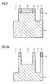
- Fig. 2 shows the first openings 11 etched in the silicon substrate material.
- the stripes of the silicon dioxide layer 20 are etched, for example in buffered hydrofluoric acid (BHF).
- BHF buffered hydrofluoric acid
- a dry etching step of etching silicon selectively with respect to silicon nitride is performed. Again this etching step is an anisotropic etching step by which a further depth of 1 F is etched.
- the structure shown in Fig. 3A is obtained.
- second openings 12 having a depth of 1 F are formed, whereas the first openings 11 now have a depth of 2F.
- the active area lines are photolithographically defined.
- a bilayer resist material is applied on the structure shown in Fig. 3A.
- the bilayer resist usually comprises two layers, a base layer which is not photoactive and a top layer which is photoactive and into which the pattern to be formed is transferred by lithographic methods.
- a lithographic step using a mask having a lines/spaces pattern is performed so as to pattern the active areas.
- the lines/spaces mask is arranged parallel to the plane of the drawing shown in Fig. 3A so that the portions shown in Fig. 4A are masked by the bilayer resist.
- the mask used has a line width of 0,8 F and a space width of 1,7 F.
- an etching step of etching silicon nitride and silicon to a target depth of 2 F is performed.
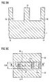
- Fig. 3B The resulting structure is shown in Fig. 3B.
- the cross-sectional view of Fig. 3B is taken perpendicular to the second openings 12 shown in Fig. 3A.
- the detailed position of the cross-sectional view between II and II can also be seen from Fig. 3C which shows a plan view on the resulting structure.
- active areas 31 are now defined in the silicon substrate material 1, the active areas 31 being delimited on either sides by isolation trenches 32. Due to the lithographic mask used, the active area has a width of 0,8 F, whereas the isolation trenches have a width of 1,7 F.
- Fig. 3C shows a plan view on the resulting structure.
- active area segments 31 are disposed in the middle of the shown plan view. Adjacent active area segments 31 are insulated from each other by the first openings 11.
- rows of active areas are insulated from each other by isolation trenches 32. The isolation trenches 32 are adjacent to the lateral sides 31a of the active areas.
- the active areas are oxidized by usual methods and, thereafter, a silicon dioxide layer 24 is deposited, for example by a HDP (high density plasma) method or a conformal deposition method.
- a wet etching step for example in buffered HF, is performed so as to recess 1,2 F depth of the deposited silicon dioxide layer 24.
- the thickness of the remaining SiO 2 material over the channel may be 0,3 F.
- an ion implantation step is performed so as to provide the first and second LDD regions 35a, 36a, i.e. the portions of the source/drain regions having a low doping concentration.
- This implantation step is performed as an angled implantation step 23, as is also illustrated in Fig. 4A, using the silicon dioxide layer 24 over the channel region as a shielding layer so that only predetermined portions of the silicon substrate between the first and the second openings 11, 12 are doped.
- an angle ⁇ between the substrate surface and the direction of the ion bombardment should be approximately 20 to 70° and, in particular, 30 to 60°.
- an angle ⁇ defining a twist angle between the implanted ions and the direction of the lateral sides 31a of the active area can be adjusted.
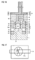
- the angle ⁇ is illustrated in Fig. 17.
- the angle ⁇ can be 0 and 90°.
- the angle ⁇ can be 45°, 135°, 225° or 315°.
- the angle ⁇ can be 60°, 120°, 240° or 300°.
- a doping of the channel region which is beneath the second opening 12 should be avoided.
- the resulting structure is shown in Fig. 4A. As can be seen, the lower portion of the first openings 11 is filled with the silicon dioxide layer 24 and the portion of the silicon substrate in which later the channel of the transistor will be formed is covered by the silicon dioxide layer 24.
- Fig. 4B shows a cross-sectional view which is taken perpendicular to the cross-sectional view in Fig. 4A so as to intersect the second openings 12.
- the silicon dioxide layer 24 is deposited so as to completely cover the active area 3 as well as to completely fill the isolation trenches 32.
- the SiO 2 layer 24 is further recessed. Thereafter, a silicon dioxide layer 26 having a thickness of 0,2 F is conformally deposited. Thereafter, an anisotropic etching step is performed. Thereby, sidewall spacers covering the lateral portions of the second openings 12 are formed. In addition, due to their narrow width, the first openings 11 are filled with SiO 2 material 26. By the etching depth of this step, the amount of side gating i.e. the interaction of the gate electrode on the first and second source/drain regions of the resultant transistor is adjusted.
- this step can be performed so as to completely remove the side wall spacers in the second openings 12, whereas the silicon dioxide layer 26 is maintained in the first openings 11 due to their narrow width.
- the width of the silicon portions between the first and the second openings in which later the source/drain regions will be formed can be larger than in the shown embodiment.
- a cleaning step with SC1 (NH 4 OH/H 2 O 2 /H 2 O) or SC2 (H 2 O 2 /HCl/H 2 O) is performed so as to remove etch damages from the channel.
- a gate oxide layer 25 is formed by generally known methods.
- an ISSG in-situ steam generated
- HTO high temperature oxide
- Fig. 5B shows a cross-sectional view taken perpendicular to the plane shown in Fig. 5A across the second openings 12.
- the isolation trenches 32 are filled with the silicon dioxide layer 24 up to a height beneath the height of the active areas 31.
- the active areas are covered by the gate oxide layer 25.
- a doped poly-silicon layer is conformally deposited above the resulting structure so as to have a thickness of 0,6 F.
- an anisotropic spacer etching step is performed to approximately 0,3 F below the silicon substrate surface 10.
- An over-etching to 0,8 F below the surface of the silicon substitute can be performed, depending on the thickness of the silicon nitride layer 21.
- the gate electrodes 33 as well as the word lines 34 are formed.
- Fig. 6A shows a cross-sectional view between I and I as can for example be seen from Fig. 6C showing a plan view on the resulting structure.
- Fig. 6B shows a cross-sectional view between II and II as can be taken from Fig. 6C.
- a gate electrode 33 is formed above the silicon dioxide layer 25.
- the first and second LDD portions 35a, 36a as well as the substrate material 1 above are insulated from the gate electrode 33 by the silicon dioxide spacer 26.
- the channel region is insulated from the gate electrode 33 by the gate oxide 25.
- Adjacent memory cells belonging to one active area line are electrically isolated from each other by the spacer 26 which is formed in the first openings 11.
- Fig. 6B shows a cross-sectional view which is taken in a direction perpendicular to the cross-sectional view of Fig. 6A intersecting the second opening 12.
- the gate electrode 33 is disposed above the active area 31 and electrically isolated therefrom by the gate oxide 25.
- the word lines 34 are formed by the spacer process as described above. Adjacent word lines 34 are electrically isolated from each other due to the openings 13 formed during the spacer process as described above.
- Fig. 6C shows a plan view on the resulting structure.
- the gate electrode 33 is disposed in the middle of the drawing and electrically connected with the word lines 34.
- two word lines 34 are adjacent to the row of active areas, wherein the two word lines 34 are connected with each other via the gate electrode 33.
- a silicon dioxide layer 27 is deposited. Thereafter, a CMP (chemical mechanical polishing) step is performed. By these steps, in particular the openings 13 as shown in Fig. 6B between adjacent word lines are filled with an insulating material. In the next step, the segments of the silicon nitride layer 21 are etched. Thereafter, an implantation step for defining the first and second source/drain regions 35, 36 having a high doping concentration is performed. The resulting structure is shown in Fig. 7.
- the resulting transistor now comprises a first and a second source/drain regions 35, 36 as well as a first LDD portion 35a and a second LDD portion 36a.
- a channel 15 is formed between the first and the second LDD portions 35a, 36a.
- a gate electrode 33 is formed above the channel, and it is electrically isolated from the channel 15 by the gate oxide layer 25.
- Side wall spacers 26 are formed between the gate electrode 33 and the first and the second source/drain regions 35 and 36. In particular, the side wall spacers 26 minimize an influence of the potential of the gate electrode on the source/drain regions 35, 36.
- the gate electrode 33 is covered by a silicon dioxide layer 27. The gate electrode 33 is disposed beneath the surface 10 of the semiconductor substrate 1.
- the top surface 33a of the gate electrode is disposed beneath the surface 10 of the semiconductor substrate 1.
- the bottom surface 33b of the gate electrode is disposed on the same height or at a smaller depth than the bottom side of the first and second LDD portions 35a, 36a.
- at least one of the first and second LDD portions 35a, 36a extends to a deeper depth than the gate electrode 33.
- bit lines are formed on the resulting surface.
- a polysilicon layer 38 and a high conductive layer such as a WSix layer 39 followed by a Si 3 N 4 layer 46, are deposited.
- a lithographic step is performed so as to define the bit lines and the bit line contacts.
- a mask having a lines/spaces pattern is used for defining the bit lines.
- the poly-silicon layer 38 and the high conductive layer 39 are etched so as to form conductive lines.
- bit line contacts can be defined using a mask having a lines/spaces pattern.
- a silicon nitride layer 40 is conformally deposited. Then, an anisotropic etching step is performed so as to provide silicon nitride spacers 40.
- a SiON liner is deposited, followed by a step of depositing a BPSG layer. Thereafter, a further CMP step is performed so as to obtain the BPSG portions 41.
- a capacitor contact 42 is photolithographically defined, etched, and filled with a conducting material such as poly-silicon. For example, the capacitor contact can be defined by using a hole mask or any other method as known in the art.
- Fig. 8 shows the resulting structure.
- the second source/drain region 36 is connected with a bit line 37, whereas the first source/drain region 35 is connected with a capacitor contact 42.
- the word lines extend in a direction which is parallel to the direction given by the lines connecting first and second source/drain regions 35 and 36.
- the word lines are disposed in a plane which lies before and behind the illustrated cross-sectional view.
- the stacked capacitor 51 which can be used with the transistor as described above can have any arbitrary shape.
- the storage capacitor 51 comprises a storage electrode 43, a capacitor dielectric 44 and a counter-electrode 45.
- the storage electrode 43 is connected with a capacitor contact 42.
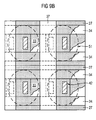
- Fig. 9B shows a plan view on the resulting memory cell array. As can be seen from Fig. 9B, a plurality of bit lines 37 are arranged in a first direction, whereas a plurality of word lines 34 are arranged in a second direction which can in particular be perpendicular to the first direction.
- Each of the word lines is connected with a plurality of gate electrodes 33.
- one row of memory cells is addressed by two parallel word lines 34 which are held on the same potential.
- Neighbouring word lines which address different rows of memory cells are electrically insulated from each other by the silicon dioxide layer 27.
- Each of the memory cells comprises a stacked capacitor 51 which is connected with a first source/drain region 35 of the corresponding transistor via a capacitor contact 42.
- Fig. 10 shows a simplified schematic diagram describing a pair of memory cell arrays 60, 60', each comprising an access transistor 52 and a storage capacitor 51 in accordance with the present invention.
- the arrays are implemented in an open bit line configuration, each employing memory cells 50, comprising one transistor 52 and one capacitor 51.
- the memory arrays 60, 60' are each coupled to respective groups of bit lines 37, 37' and respective groups of word lines 34a, 34b, 34a, 34b'.
- the two groups of bit lines 37, 37' are coupled, one from each of the memory arrays 60, 60' to sense amplifiers 6.
- the sense amplifiers 6 comprise peripheral circuitry, generally formed outside of the memory cell arrays 60, 60'.
- one memory cell 6 is selected, for example, by activating one pair of word lines 34a, 34b, the word lines of one pair being held at the same potential.
- the pair of word lines 34a, 34b is coupled to the respective gate electrode of a respective one of the transistors 52.
- the bit line 37 is coupled to the second source/drain region of one of these transistors 52 via bit line contacts.
- the transistor 52 is turned on, coupling charge stored in the capacitor 51 to the associated bit line 37.
- the sense amplifier 6 then senses the charge coupled from the capacitor 51 to the bit line 37.
- the sense amplifier 6 compares that signal to a reference signal, such as the reference charge Qref or a reference signal which is obtained by sensing a corresponding bit line 37', without a voltage being applied to the corresponding pair of word lines 34a', 34b', and amplifies the resulting signal.
- a reference signal such as the reference charge Qref or a reference signal which is obtained by sensing a corresponding bit line 37', without a voltage being applied to the corresponding pair of word lines 34a', 34b', and amplifies the resulting signal.
- the capacitor covers an area of 2,4 ⁇ 1,8 F 2 , and the cell size is 2,6 F length 3 F width.
- the active area has the shape of a ridge, wherein the gate-electrode is disposed a three sides thereof.
- the transistor having the shape of such a FINFET can be implemented with any arbitrary cell size.
- a silicon dioxide layer 20 is deposited on the surface 10 of the semiconductor substrate 1. Thereafter, the lithographic step is performed using a mask having a lines/spaces pattern. In contrast to the first embodiment, the line width is 0,8 F whereas the space width is 1,2 F. After etching the spaces, a silicon nitride layer is deposited by generally known methods and etched so as to have a width of 0,3 F. Thereby, stripes 21 of a silicon nitride layer are formed. In a next step, a nitridation step for providing a diffusion barrier is performed, followed by a step of depositing a BPSG layer. The BPSG layer is annealed, and thereafter, a CMP step is performed.
- Figs. 11A and 11B the structure shown in Figs. 11A and 11B is obtained.
- Fig. 11B in a similar manner as in Fig. 1B, the surface of the semiconductor substrate now is covered by stripes of a SiO 2 layer 20, which is delimited on either sides by Si 3 N 4 stripes 21, two Si 3 N 4 stripes 21 enclosing one BPSG stripe 22.
- the width of the SiO 2 lines 20 amounts to 0,8 F.
- the process steps which have been described with reference to Figs. 2 and 3 are performed and a description thereof is omitted.
- a silicon dioxide layer 24 is formed in the same manner as has been described above.
- an etching step is performed, for example in buffered HF to expose the channel region.
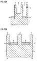
- Fig. 12A shows a cross-section between I and I similar to the cross-sectional view shown in Fig. 4A except for the lateral dimensions of the first and second openings 11, 12, respectively.
- the silicon dioxide material which has been filled in the first openings 11, is removed in the upper portion of the first openings 11.
- Fig. 12B the insulating material 24 in the isolation trenches 32 now only is present in the lower portion thereof.
- a silicon dioxide layer 26, having a thickness of 0,2 F is conformally deposited.
- an anisotropic etching step is performed.
- sidewall spacers covering the lateral portions of the second openings 12 are formed.
- a cleaning step with SC1 or SC2 is performed so as to remove etch damages from the channel.
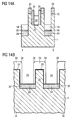
- a gate oxide layer 25 is formed in the same manner as has been described with respect to Fig. 5A. The resulting structure is shown in Fig. 13A.
- Fig. 13B shows a cross-sectional view of the resulting structure, this cross-sectional view being taken perpendicular to the active area 31.
- the silicon dioxide material 24 provided in the isolation trenches 32 now is recessed, and a thin gate oxide layer 25 is provided on the sidewalls of the active area 31.
- a doped poly-silicon layer is conformally deposited above the resulting structure so as to have a thickness of 0,5 F.
- an anisotropic spacer etching step is performed to 0,3 F below the silicon substrate surface 10. This etching step is performed in a similar manner as the etching process which has been described with reference to Fig. 6A.
- the gate electrodes 33 as well as the word lines 34 are formed.
- Fig. 14C shows a plan view on the resulting memory cell array.
- the gate electrode 33 is disposed in the middle of the drawing and electrically connected with the word lines 34.
- two word lines 34 are adjacent to the row of active areas, wherein the two word lines 34 are connected with each other via the gate electrode 33.
- a self-aligned source/drain ion implantation step is performed so as to provide the first and second source/drain regions 35, 36 including the first and second portions having a low doping concentration 35a, 36a.
- the ion implantation step for providing the portions having a low doping concentration is also performed with an angled implantation, as has been described before, wherein the gate electrodes 33 are used as a shielding layer.
- the angles ⁇ and ⁇ can be adjusted in the manner as described above with reference to Fig. 4. In this respect, if a certain value of the angle ⁇ is adjusted and the sidewalls of the portion to be implanted are covered by a shielding layer, the effective thickness of the shielding layer depends on the twist angle ⁇ .
- the ion implantation step for providing the portions having a high doping concentration is performed in a conventional manner, in particular, by a perpendicular ion implantation.
- the capacitor now has a lateral dimension of 1,7 ⁇ 2 F, and the cell size is 2 F length ⁇ 2.3 F width, resulting in a cell area of 4,6 F 2 .
- the transistor now is a FINFET-type transistor having a channel in the shape of a ridge. Accordingly, the effective width of the channel is enlarged. At the same time, due to the narrow width of the ridge, the channel can be fully depleted.
- Fig. 16 shows a cross-sectional view of the memory cell in which the spacer which is shown in Fig. 15 is omitted and replaced by a gate insulating layer 25.
Landscapes
- Engineering & Computer Science (AREA)
- Manufacturing & Machinery (AREA)
- Semiconductor Memories (AREA)
Abstract
The present invention refers to a memory cell array comprising a plurality of active areas in which a plurality of memory cells are formed. A memory cell comprises a storage capacitor, a transistor which is at least partially formed in a semiconductor substrate having a substrate surface, said transistor comprising a first source/drain region, said first source/drain region being formed adjacent to said substrate surface, a second source/drain region being formed adjacent to said substrate surface, a channel region connecting said first and second source/drain regions, said channel region being disposed in said semiconductor substrate, and a gate electrode. Rows of the active areas are separated from each other by isolation grooves which extend along a first direction. A first and a second word lines are disposed on either lateral sides of each of the rows of active areas, the first and the second word lines being connected with each other via the gate electrodes of the transistors of the corresponding row of active areas.
Description
- The present invention relates to a memory cell array as well as to a method of manufacturing a memory cell array.
- Memory cells of a dynamic random access memory (DRAM) generally comprise a storage capacitor for storing an electrical charge which represents an information to be stored, and an access transistor connected with the storage capacitor. The access transistor comprises a first and a second source/drain regions, a channel connecting the first and second source/drain regions as well as a gate electrode controlling an electrical current flowing between the first and second source/drain regions. The transistor usually is at least partially formed in a semiconductor substrate. The information stored in the storage capacitor is read out or written in by addressing the access transistor via the corresponding word line. In particular, the information is read out to a corresponding bit line via a bit line contact.
- There is a lower boundary of the channel length of the access transistor, below which the insulation properties of the access transistor in a non-addressed state are not sufficient. The lower boundary of the effective channel length Leff limits the scalability of planar transistor cells having an access transistor which is horizontally formed with respect to the substrate surface of the semiconductor substrate.
- Vertical transistor cells offer a possibility of enhancing the channel length while maintaining the surface area necessary for forming the memory cell. In such a vertical transistor cell the source/drain regions of the access transistor as well as the channel region are arranged in a direction perpendicular to the substrate surface. One of the problems involved with such a vertical transistor cell is the difficulty in providing a surface contact to a stacked capacitor. Accordingly, such a vertical transistor is difficult to integrate with a stacked capacitor.
- A concept, in which the effective channel length Leff is enhanced, refers to a recessed channel transistor, as is for example known from
US Patent No. 5,945,707 the disclosure of which is incorporated herein by reference in its entirety. In such a transistor, the first and second source/drain regions are arranged in a horizontal plane parallel to the substrate surface. The gate electrode is arranged in a recess groove, which is disposed between the two source/drain regions of the transistor in the semiconductor substrate. Accordingly, the effective channel length equals to the sum of the distance between the two source/drain regions and the two fold of the depth of the recess groove. The effective channel width Weff corresponds to the nominal structural size F. - Furthermore,
U.S. Patent No. 5,502,320 , the disclosure of which is incorporated herein by reference in its entity, discloses a memory cell array in which transistors are formed in continuous active area lines. The active area lines are arranged in parallel with the bit lines. In particular, the gate electrodes of the transistors from part from the word lines and the word lines including the gate electrodes are implemented as buried word lines. - In addition
DE 103 61 695 B3 , the disclosure of which is incorporated herein by reference in its entity, discloses a transistor which is formed in an active area having the form of a ridge, wherein two gate electrodes each forming part of a corresponding word lines are disposed along the lateral sides of the active area. The active area is recessed at a channel portion of the transistor. - It is an object of the invention to provide an improved memory cell array as well as an improved method of forming such a memory cell array.
- According to the present invention, the above object is achieved by the memory cell array of
claim 1. Moreover, the object is achieved by the method of forming a memory cell array as defined inclaim 14. The preferred embodiments of the present invention are set forth in the dependent claims. - In particular, the present invention provides a memory cell array comprising a plurality of memory cells, the memory cell array comprising a plurality of active areas being formed in a semiconductor substrate having a substrate surface, each of said active areas having two lateral sides extending along a first direction, rows of said active areas being separated from each other by isolation grooves extending along said first direction, each of said memory cells comprising a storage capacitor, a transistor which is at least partially formed in one of said active areas, said transistor comprising a first source/drain region which is connected with an electrode of said storage capacitor, said first source/drain region being formed adjacent to said substrate surface, a second source/drain region being formed adjacent to said substrate surface, a channel region connecting said first and second source/drain regions, said channel region being disposed in said active area, said channel region extending along said first direction, and a gate electrode disposed along said channel region and being electrically isolated from said channel region by a gate insulating layer, said gate electrode controlling an electrical current flowing between said first and second source/drain regions, wherein a first and a second word lines are disposed on either lateral sides of each of said rows of active areas, said first and said second word lines being connected with each other via the gate electrodes of the transistors of the corresponding row of active areas.
- In particular, according to the present invention, the word lines including the gate electrodes form a kind of a ladder structure according to which two word lines of the memory cell array are arranged in parallel with the channel. The channel is crossed by a gate electrode which connects the two word lines. Accordingly, the advantage is obtained that the word lines can be formed without employing special lithographic steps.
- In particular, according to a preferred embodiment, two word lines can be disposed in each of said isolation grooves, the two word lines being insulated from each other and being assigned to two different rows of active areas. In this case, the word lines can easily be formed by a spacer process without the necessity of performing lithographic steps. In addition, the exact positioning of the word lines is ensured since the step of forming the word lines is performed self-aligned with respect to the isolation grooves and, consequently, the active areas.
- According to a preferred embodiment, each of the gate electrode has a top side, said top side of said gate electrode being disposed beneath said surface of said semiconductor substrate. As a consequence, the channel connecting first and second source/drain regions is implemented as a curved or recessed channel. In particular, the active area has the shape of a "U", wherein the first and second source/drain regions are disposed in the vertical portions of the active area. In addition, the ladder structure of the word lines including the gate electrodes is supported by the vertical portion of the active areas in which the first and second source/drain regions are formed. Thereby, the advantage is achieved that the word lines including the gate electrodes are formed in a self-aligned manner with respect to the first and second source/drain regions.
- If the active area has the shape of a "U" and the channel is a curved or recessed channel, a distance between the doped source/drain regions can be enlarged without increasing the area of the transistor. Due to the enlarged distance, an electrical field at the source/drain region - channel junction and, hence, a leakage current is decreased.
- Nevertheless, the special structure of two adjacent word lines and the corresponding gate electrodes, by which structure a ladder is formed, can be implemented with any arbitrary shape of the active area.
- Preferably, the channel region comprises a fin-region in which the channel has the shape of a ridge, said ridge comprising a top side and two lateral sides in a cross section perpendicular to a line connecting said first and second source/drain regions, and wherein said gate electrode is disposed at three sides of said ridge.
- In this case, the effective width of the channel is enlarged improving the characteristics of the transistor. In particular, the transistor of the memory cell array of the present invention provides an improved on-current in comparison with known transistors, since the width of the channel is increased whereby the resistance is reduced. Nevertheless, due to the narrow width of the fin region, the transistor body can be fully depleted, so that the off-current of the transistor can be improved.
- Nevertheless, the special structure of two adjacent word lines and the corresponding gate electrodes, by which structure a ladder is formed, can be implemented with any arbitrary shape of the channel region.
- In particular, the storage capacitor can be implemented as a stacked capacitor.
- According to the invention, preferably, the plurality of memory cells are arranged in rows and columns, respectively, two adjacent rows of memory cells being separated by two word lines that are electrically isolated from each other, wherein the memory cells are arranged in the form of a regular grid.
- In particular, the memory cells of adjacent rows are disposed in the same columns, respectively. In addition, the memory cells of adjacent columns are disposed in the same rows, respectively.
- According to the invention, it is preferred that the gate electrode has a bottom side, each of said first and second source/drain regions extending to a depth below or equal to said bottom side of said gate electrode.
- Preferably, the bit lines are formed on the substrate surface. In particular, it is preferred that the bit lines are directly adjacent to the substrate surface so that the bit lines are connected with the second source/drain regions without the necessity of a bit line contact.
- It is further preferred that an insulating spacer is disposed between said first source/drain region and said gate electrode and between said second source/drain region and said gate electrode, said insulating spacer having a larger thickness than said gate insulating layer. In this case, the influence of the potential of the gate electrode on the first and second source/drain regions can be lowered. In particular, by effectively shielding the gate potential from the first source/drain region which is connected with an electrode of a storage capacitor the retention time of the memory cell, i.e. the time during which an information can be recognizably stored in the memory cell, can be improved. At the same time, since the thickness of the gate insulating layer is smaller than that of the insulating spacer, the conductivity of the channel can be effectively controlled.
- In particular, if the spacer is made of silicon dioxide, the influence of the gate electrode on the first and second source/drain regions can further be lowered.
- The present invention further provides a method of manufacturing a memory cell array comprising the steps of providing a semiconductor substrate having a substrate surface, forming first and second openings in said substrate surface, said first openings having a larger depth than said second openings, said depth being measured from said substrate surface, two first openings being followed by one second opening, and one second opening being followed by two first openings, defining isolation trenches in said semiconductor substrate, active areas being formed between two adjacent isolation trenches, filling said isolation trenches with an insulating material, providing a gate insulating layer on a bottom side of said second openings, providing a conductive material in said second openings and on the side walls of said isolation trenches, gate electrodes being formed of the conductive material in said second openings and word lines being formed of the conductive material on the side walls of said isolation trenches, providing an insulating material on the top side of said gate electrodes and between the word lines of one isolation trench, providing first and second source/drain regions in said substrate material between said first and second openings in an active area, forming a plurality of bit line contacts and bit lines, one bit line being connected with a plurality of second source/drain regions via said bit line contacts, forming a plurality of capacitor contacts, each of said capacitor contact being connected with said first source/drain region of a memory cell, forming a plurality storage capacitors, each of said storage capacitors being in contact with one of said capacitor contacts.
- In particular, by forming the first openings in the substrate surface, an electrical isolation between adjacent memory cells of one row of the corresponding array is provided. Differently speaking, thereby, the active area is segmented.
- In addition, by forming the second openings, the gate electrodes are defined. In addition, the vertical portions of the active areas in which the first and second source/drain portions are to be formed are defined. According to the present invention, the isolation trenches are formed after defining the vertical portions of the active areas in which the first and second source/drain portions are to be formed. As a consequence, the isolation trenches are formed in a self-aligned manner with respect to the first and second source/drain portions.
- According to the invention, it is especially preferred that said first and second openings are defined using a hardmask comprising first, second and third stripes of a first, a second, and a third material, respectively, the first, second and third stripes being arranged parallel to each other, and each of the first, second and third material being able to be etched selectively to each other.
- Thereby, it is very easy to form the first and second openings in the correct position.
- In addition, it is preferred that the depth of the first openings is equal to the depth of said isolation trenches, said depth being measured from said substrate surface.
- Preferably, before the step of forming the plurality of bit lines, the first and second source/drain regions are not masked, whereas all the remaining portions of the surface are covered by an insulating material.
- Thereby, it is possible to form the bit lines so as to be in contact with the second source/drain regions of the transistors in a self-aligned manner.
- According to the invention, the step of forming the plurality of bit lines preferably comprises the steps of depositing at least one layer of a conductive material and patterning said at least one layer so as to form bit lines which are in contact with the second source/drain regions of the transistors.
- In addition, it is preferred that at least one layer is photolithographically patterned using a mask having a lines/spaces pattern. Thereby, the correct positioning of the mask is simplified since a mask having a lines/spaces pattern is easier to handle and to position.
- According to the invention, the step of providing a conductive material preferably comprises the steps of conformally depositing said conductive material and anisotropically etching said conductive material.
- Preferably, the method of the invention further comprises the step of providing a first and a second lightly doped portions, said step being performed after the step of filling said isolation trenches with an insulating material, comprising the steps of providing an insulating material in said second opening, conducting an angled ion implantation step at an angle α between said substrate surface and a direction of said ions. Thereby, it is possible to implant a predetermined substrate portion beneath the substrate surface.
- The method of the invention preferably comprises the step of removing the upper part of said insulating material from said isolation trenches so as to expose the upper part of said active area before providing said gate insulating layer, said gate insulating layer being formed on the exposed portions of said active area.
- Thereby, a FINFET in which the channel has the shape of a ridge can easily be formed.
- In this case, the step of providing first and second source/drain regions preferably comprises the step of providing a first and a second lightly doped portions, said step being performed after the step of providing an insulating material on the top side of said gate electrodes and between the word lines of one isolation trench, the step of providing a first and a second lightly doped portions being performed by conducting an angled ion implantation step at an angle α between said substrate surface and a direction of said ions.
- In particular, by conducting such an angled ion implantation step, by adjusting the angle α, the doping profile of the doped portions can be arbitrarily adjusted. In particular, the depth and the distribution of the dopants in the active areas can be adjusted.
- The accompanying drawings are included to provide a further understanding of the present invention and are incorporated in and constitute a part of the specification. The drawings illustrate the embodiments of the present invention and together with the description serve to explain the principles of the invention. Other embodiments of the present invention and many of the intended advantages of the present invention will be readily appreciated as they become better understood by reference to the following detailed description. The elements of the drawings are not necessarily to scale relative to each other. Like reference numerals designate corresponding similar parts.
- Figs. 1 to 9
- illustrate steps of a method of manufacturing a memory cell array according to a first embodiment of the present invention;
- Fig. 10
- shows an exemplary layout of the memory cell array of the present invention,
- Fig. 11 to 15
- illustrate steps of a method of manufacturing a memory cell array according to a second embodiment of the present invention,
- Fig. 16
- shows part of a memory cell array according to a further embodiment of the present invention, and
- Fig. 17
- shows a diagrammatic view for illustrating the angled implantation step.
- In the following detailed description, reference is made to accompanying drawings which form a part hereof and in which is illustrated by way of illustration, specific embodiments in which the invention may be practiced. In this regard, directional terminology, such as "top", "bottom", "front", "back", "leading", "trailing", etc., is used with reference to the orientation of the Figures being described. Because components of the embodiments of the present invention can be positioned in a number of different orientations, the directional terminology is used for purposes of illustration and is no way limiting. It is to be understood that other embodiments may be utilized and structural or logical changes will be made without departing from the scope of the present invention. The following detailed description, therefore, is not to be taken in a limiting sense, and the scope of the present invention is defined by the appended claims.
- For manufacturing the memory cell array of the present invention, first, a silicon dioxide (SiO2)
layer 20 having a thickness of 70 to 100 nm is deposited as a first hard mask layer. Thereafter, the SiO2 layer 20 is photolithographically patterned using a mask having a lines/spacers pattern. In particular, for the first embodiment, the lithographic mask used has a pattern having a line width of 1,4 F and a space width of 1,2 F. In this regard, F denotes the minimum line width of the feature size which can be obtained by the technology used. In particular F can be less than 100 nm and, in particular, 90, 70 or even 40 nm. Thereafter, a silicon nitride (Si3N4)layer 21 is conformally deposited by generally known methods. In particular, the Si3N4 layer 21 can have a thickness of approximately 0,3 F. Thereafter, an anisotropic etching step is performed so as to expose the horizontal portions of thesilicon dioxide layer 20 and thesilicon substrate 1. As a consequence, the sidewalls of the spaces of the SiO2 layer 20 are covered by Si3N4 spacers 21. - In the next step a nitridation step as is generally known is performed so as to provide a diffusion barrier. To be more specific, a thin Si3N4 layer is formed, for example, by exposing the substrate to a NH3 atmosphere. This thin Si3N4 layer prevents boron atoms from outdiffusing from the BPSG layer which is to be formed in the next step.
- Thereafter a BPSG layer is deposited by generally known methods, an annealing step is performed and thereafter a CMP step is conducted so that finally the structure shown in Fig. 1A is obtained.
- In particular, Fig. 1A shows a cross-sectional view of the resulting structure. On the
surface 10 of asemiconductor substrate 1, such as a silicon substrate, a stripe of asilicon dioxide layer 20 having a width of 1,4 F is formed. On both sides of thesilicon dioxide layer 20,stripes 21 of asilicon nitride layer 21 are arranged, followed by stripes of aBPSG layer 22. In particular, the width of thesilicon nitride stripes 21 is approximately 0,3 F, whereas the width of thestripes 22 of the BPSG layer is approximately 0,6 F. - Fig. 1B shows a plan view of the resulting structure. As can be seen, the
whole surface 10 of thesemiconductor substrate 1 is covered by stripes of asilicon dioxide layer 20,parallel stripes 21 of a silicon nitride layer andparallel stripes 22 of a BPSG layer. As is to be noted from Fig. 1B, the cross-sectional view of Fig. 1A is taken between I and I in Fig. 1B. - In the next step, the stripes of the
BPSG layer 22 are etched selectively with respect to silicon dioxide. For example, an etching step in HF vapour can be used for etching the BPSG layer. In the next step, the silicon substrate is etched selectively with respect to silicon dioxide and silicon nitride so as to formfirst openings 11. In particular, a dry etching step as commonly used is performed so that the silicon material is etched anisotropically to a target depth of 1 F. In this etching step, the stripes of thesilicon dioxide layer 20 and thesilicon nitride layer 21 act as a hard mask. - The resulting structure is shown in Fig. 2. In particular Fig. 2 shows the
first openings 11 etched in the silicon substrate material. - In the next step, the stripes of the
silicon dioxide layer 20 are etched, for example in buffered hydrofluoric acid (BHF). Thereafter, a dry etching step of etching silicon selectively with respect to silicon nitride is performed. Again this etching step is an anisotropic etching step by which a further depth of 1 F is etched. As a result, the structure shown in Fig. 3A is obtained. In particular, in the cross-sectional view shown in Fig. 3A, by the last etching step,second openings 12 having a depth of 1 F are formed, whereas thefirst openings 11 now have a depth of 2F. - In the next step, the active area lines are photolithographically defined. In particular, a bilayer resist material is applied on the structure shown in Fig. 3A. The bilayer resist usually comprises two layers, a base layer which is not photoactive and a top layer which is photoactive and into which the pattern to be formed is transferred by lithographic methods. By using a bilayer resist, problems caused by a topography of the wafer surface can be eliminated.
- Thereafter a lithographic step using a mask having a lines/spaces pattern is performed so as to pattern the active areas. In particular the lines/spaces mask is arranged parallel to the plane of the drawing shown in Fig. 3A so that the portions shown in Fig. 4A are masked by the bilayer resist. The mask used has a line width of 0,8 F and a space width of 1,7 F. Thereafter, an etching step of etching silicon nitride and silicon to a target depth of 2 F is performed.
- The resulting structure is shown in Fig. 3B. In particular, the cross-sectional view of Fig. 3B is taken perpendicular to the
second openings 12 shown in Fig. 3A. The detailed position of the cross-sectional view between II and II can also be seen from Fig. 3C which shows a plan view on the resulting structure. - As can be seen from Fig. 3B,
active areas 31 are now defined in thesilicon substrate material 1, theactive areas 31 being delimited on either sides byisolation trenches 32. Due to the lithographic mask used, the active area has a width of 0,8 F, whereas the isolation trenches have a width of 1,7 F. - In addition Fig. 3C shows a plan view on the resulting structure. In particular,
active area segments 31 are disposed in the middle of the shown plan view. Adjacentactive area segments 31 are insulated from each other by thefirst openings 11. In addition, rows of active areas are insulated from each other byisolation trenches 32. Theisolation trenches 32 are adjacent to thelateral sides 31a of the active areas. - In the next step the active areas are oxidized by usual methods and, thereafter, a
silicon dioxide layer 24 is deposited, for example by a HDP (high density plasma) method or a conformal deposition method. Thereafter, a wet etching step, for example in buffered HF, is performed so as to recess 1,2 F depth of the depositedsilicon dioxide layer 24. For example, the thickness of the remaining SiO2 material over the channel may be 0,3 F. Thereafter, an ion implantation step is performed so as to provide the first andsecond LDD regions - This implantation step is performed as an
angled implantation step 23, as is also illustrated in Fig. 4A, using thesilicon dioxide layer 24 over the channel region as a shielding layer so that only predetermined portions of the silicon substrate between the first and thesecond openings - In particular, an angle α between the substrate surface and the direction of the ion bombardment should be approximately 20 to 70° and, in particular, 30 to 60°. By adjusting the angle of the ion implantation, the penetration depth and, consequently, the doping profile can be adjusted to a predetermined one.
- Moreover, an angle δ defining a twist angle between the implanted ions and the direction of the
lateral sides 31a of the active area can be adjusted. The angle δ is illustrated in Fig. 17. In a dual mode ion implantation step in which the ion implantation is conducted from two directions differing by 180°, the angle δ can be 0 and 90°. In a quad mode ion implantation step in which the ion implantation is performed from four directions differing by 90°, the angle δ can be 45°, 135°, 225° or 315°. Alternatively, in a quad mode ion implantation step, the angle δ can be 60°, 120°, 240° or 300°. - In particular, a doping of the channel region which is beneath the
second opening 12 should be avoided. The resulting structure is shown in Fig. 4A. As can be seen, the lower portion of thefirst openings 11 is filled with thesilicon dioxide layer 24 and the portion of the silicon substrate in which later the channel of the transistor will be formed is covered by thesilicon dioxide layer 24. - Fig. 4B shows a cross-sectional view which is taken perpendicular to the cross-sectional view in Fig. 4A so as to intersect the
second openings 12. As can be seen from Fig. 4B, thesilicon dioxide layer 24 is deposited so as to completely cover the active area 3 as well as to completely fill theisolation trenches 32. - In the next step, the SiO2 layer 24 is further recessed. Thereafter, a
silicon dioxide layer 26 having a thickness of 0,2 F is conformally deposited. Thereafter, an anisotropic etching step is performed. Thereby, sidewall spacers covering the lateral portions of thesecond openings 12 are formed. In addition, due to their narrow width, thefirst openings 11 are filled with SiO2 material 26. By the etching depth of this step, the amount of side gating i.e. the interaction of the gate electrode on the first and second source/drain regions of the resultant transistor is adjusted. - As a modification, this step can be performed so as to completely remove the side wall spacers in the
second openings 12, whereas thesilicon dioxide layer 26 is maintained in thefirst openings 11 due to their narrow width. In addition, according to a further modification, the width of the silicon portions between the first and the second openings in which later the source/drain regions will be formed, can be larger than in the shown embodiment. - Thereafter, a cleaning step with SC1 (NH4OH/H2O2/H2O) or SC2 (H2O2/HCl/H2O) is performed so as to remove etch damages from the channel. Thereafter, a
gate oxide layer 25 is formed by generally known methods. In particular, an ISSG (in-situ steam generated) silicon dioxide layer can be formed or a HTO (high temperature oxide) can be formed. The resulting structure is shown in Fig. 5A. As can be seen, in the bottom portion of thesecond openings 12, thegate oxide 25 is formed. The side walls of the second openings are covered by thesilicon dioxide layer 26, and the first openings are completely filled withsilicon dioxide material 26. - Fig. 5B shows a cross-sectional view taken perpendicular to the plane shown in Fig. 5A across the
second openings 12. - As can be seen from Fig. 5B, the
isolation trenches 32 are filled with thesilicon dioxide layer 24 up to a height beneath the height of theactive areas 31. The active areas are covered by thegate oxide layer 25. - In the next step, a doped poly-silicon layer is conformally deposited above the resulting structure so as to have a thickness of 0,6 F. Thereafter, an anisotropic spacer etching step is performed to approximately 0,3 F below the
silicon substrate surface 10. An over-etching to 0,8 F below the surface of the silicon substitute can be performed, depending on the thickness of thesilicon nitride layer 21. - By this step, the
gate electrodes 33 as well as the word lines 34 are formed. - The resulting structure is shown in Fig. 6. In particular, Fig. 6A shows a cross-sectional view between I and I as can for example be seen from Fig. 6C showing a plan view on the resulting structure. Moreover, Fig. 6B shows a cross-sectional view between II and II as can be taken from Fig. 6C.
- In particular, as is shown in Fig. 6A, a
gate electrode 33 is formed above thesilicon dioxide layer 25. The first andsecond LDD portions substrate material 1 above are insulated from thegate electrode 33 by thesilicon dioxide spacer 26. The channel region is insulated from thegate electrode 33 by thegate oxide 25. Adjacent memory cells belonging to one active area line are electrically isolated from each other by thespacer 26 which is formed in thefirst openings 11. - In addition, Fig. 6B shows a cross-sectional view which is taken in a direction perpendicular to the cross-sectional view of Fig. 6A intersecting the
second opening 12. As can be seen from Fig. 6B, thegate electrode 33 is disposed above theactive area 31 and electrically isolated therefrom by thegate oxide 25. On the side walls of theisolation trenches 32 the word lines 34 are formed by the spacer process as described above. Adjacent word lines 34 are electrically isolated from each other due to theopenings 13 formed during the spacer process as described above. - Fig. 6C shows a plan view on the resulting structure. As can be seen, the
gate electrode 33 is disposed in the middle of the drawing and electrically connected with the word lines 34. In particular, twoword lines 34 are adjacent to the row of active areas, wherein the twoword lines 34 are connected with each other via thegate electrode 33. - In the next step, a
silicon dioxide layer 27 is deposited. Thereafter, a CMP (chemical mechanical polishing) step is performed. By these steps, in particular theopenings 13 as shown in Fig. 6B between adjacent word lines are filled with an insulating material. In the next step, the segments of thesilicon nitride layer 21 are etched. Thereafter, an implantation step for defining the first and second source/drain regions - As can be seen from Fig. 7, the resulting transistor now comprises a first and a second source/
drain regions first LDD portion 35a and asecond LDD portion 36a. Achannel 15 is formed between the first and thesecond LDD portions gate electrode 33 is formed above the channel, and it is electrically isolated from thechannel 15 by thegate oxide layer 25.Side wall spacers 26 are formed between thegate electrode 33 and the first and the second source/drain regions side wall spacers 26 minimize an influence of the potential of the gate electrode on the source/drain regions gate electrode 33 is covered by asilicon dioxide layer 27. Thegate electrode 33 is disposed beneath thesurface 10 of thesemiconductor substrate 1. In particular, thetop surface 33a of the gate electrode is disposed beneath thesurface 10 of thesemiconductor substrate 1. In addition, the bottom surface 33b of the gate electrode is disposed on the same height or at a smaller depth than the bottom side of the first andsecond LDD portions second LDD portions gate electrode 33. - In the next step, the bit lines are formed on the resulting surface. In particular, a
polysilicon layer 38 and a high conductive layer such as aWSix layer 39 followed by a Si3N4 layer 46, are deposited. Thereafter, a lithographic step is performed so as to define the bit lines and the bit line contacts. In particular, a mask having a lines/spaces pattern is used for defining the bit lines. Thereafter, the poly-silicon layer 38 and the highconductive layer 39 are etched so as to form conductive lines. - In particular since the whole substrate surface except for the portions over which the
silicon nitride segments 21 have been present now is covered by the silicon dioxide layer, bit line contacts can be defined using a mask having a lines/spaces pattern. - In the next step a
silicon nitride layer 40 is conformally deposited. Then, an anisotropic etching step is performed so as to providesilicon nitride spacers 40. In the next step, a SiON liner is deposited, followed by a step of depositing a BPSG layer. Thereafter, a further CMP step is performed so as to obtain theBPSG portions 41. In the next step, acapacitor contact 42 is photolithographically defined, etched, and filled with a conducting material such as poly-silicon. For example, the capacitor contact can be defined by using a hole mask or any other method as known in the art. - Fig. 8 shows the resulting structure. The second source/
drain region 36 is connected with abit line 37, whereas the first source/drain region 35 is connected with acapacitor contact 42. The word lines extend in a direction which is parallel to the direction given by the lines connecting first and second source/drain regions - In the next step, the conventional process steps for forming a stacked capacitor are conducted. The stacked
capacitor 51 which can be used with the transistor as described above can have any arbitrary shape. For example, it can have the construction as shown in Fig. 9A. In particular, thestorage capacitor 51 comprises astorage electrode 43, acapacitor dielectric 44 and a counter-electrode 45. Thestorage electrode 43 is connected with acapacitor contact 42. Fig. 9B shows a plan view on the resulting memory cell array. As can be seen from Fig. 9B, a plurality ofbit lines 37 are arranged in a first direction, whereas a plurality ofword lines 34 are arranged in a second direction which can in particular be perpendicular to the first direction. Each of the word lines is connected with a plurality ofgate electrodes 33. In particular, one row of memory cells is addressed by twoparallel word lines 34 which are held on the same potential. Neighbouring word lines which address different rows of memory cells are electrically insulated from each other by thesilicon dioxide layer 27. Each of the memory cells comprises a stackedcapacitor 51 which is connected with a first source/drain region 35 of the corresponding transistor via acapacitor contact 42. - Fig. 10 shows a simplified schematic diagram describing a pair of
memory cell arrays 60, 60', each comprising anaccess transistor 52 and astorage capacitor 51 in accordance with the present invention. The arrays are implemented in an open bit line configuration, each employingmemory cells 50, comprising onetransistor 52 and onecapacitor 51. - The
memory arrays 60, 60' are each coupled to respective groups ofbit lines 37, 37' and respective groups ofword lines bit lines 37, 37' are coupled, one from each of thememory arrays 60, 60' to senseamplifiers 6. Thesense amplifiers 6 comprise peripheral circuitry, generally formed outside of thememory cell arrays 60, 60'. - In operation, one
memory cell 6 is selected, for example, by activating one pair ofword lines word lines transistors 52. Thebit line 37 is coupled to the second source/drain region of one of thesetransistors 52 via bit line contacts. Thetransistor 52 is turned on, coupling charge stored in thecapacitor 51 to the associatedbit line 37. Thesense amplifier 6 then senses the charge coupled from thecapacitor 51 to thebit line 37. Thesense amplifier 6 compares that signal to a reference signal, such as the reference charge Qref or a reference signal which is obtained by sensing a corresponding bit line 37', without a voltage being applied to the corresponding pair ofword lines 34a', 34b', and amplifies the resulting signal. This allows data represented by the charge stored in thecapacitor 51 to be accessed external to thememory arrays 60, 60' and also allows thecapacitor 51 to store charge representative of the data from thememory cell 50 back into thememory cell 50. - In the shown layout of the first embodiment, the capacitor covers an area of 2,4 ·1,8 F2, and the cell size is 2,6 F length 3 F width.
- According to a second embodiment of the present invention a smaller cell size is obtained. In addition, according to the second embodiment, the active area has the shape of a ridge, wherein the gate-electrode is disposed a three sides thereof. As is obvious to the person skilled in the art, the transistor having the shape of such a FINFET can be implemented with any arbitrary cell size.
- For implementing the second embodiment, a
silicon dioxide layer 20 is deposited on thesurface 10 of thesemiconductor substrate 1. Thereafter, the lithographic step is performed using a mask having a lines/spaces pattern. In contrast to the first embodiment, the line width is 0,8 F whereas the space width is 1,2 F. After etching the spaces, a silicon nitride layer is deposited by generally known methods and etched so as to have a width of 0,3 F. Thereby,stripes 21 of a silicon nitride layer are formed. In a next step, a nitridation step for providing a diffusion barrier is performed, followed by a step of depositing a BPSG layer. The BPSG layer is annealed, and thereafter, a CMP step is performed. - As a result, the structure shown in Figs. 11A and 11B is obtained. As can be seen from Fig. 11B, in a similar manner as in Fig. 1B, the surface of the semiconductor substrate now is covered by stripes of a SiO2 layer 20, which is delimited on either sides by Si3N4 stripes 21, two Si3N4 stripes 21 enclosing one
BPSG stripe 22. The width of the SiO2 lines 20 amounts to 0,8 F. In the following, the process steps which have been described with reference to Figs. 2 and 3 are performed and a description thereof is omitted. After etching the isolation trenches so as to define the active areas, asilicon dioxide layer 24 is formed in the same manner as has been described above. - After filling the isolation trenches with the
silicon dioxide layer 24, an etching step is performed, for example in buffered HF to expose the channel region. - The resulting structure is shown in Fig. 12. In particular, Fig. 12A shows a cross-section between I and I similar to the cross-sectional view shown in Fig. 4A except for the lateral dimensions of the first and
second openings first openings 11, is removed in the upper portion of thefirst openings 11. As can be also seen from Fig. 12B, the insulatingmaterial 24 in theisolation trenches 32 now only is present in the lower portion thereof. - Thereafter, a
silicon dioxide layer 26, having a thickness of 0,2 F is conformally deposited. Then, an anisotropic etching step is performed. Thereby, sidewall spacers covering the lateral portions of thesecond openings 12 are formed. These steps of forming the sidewall spacers by conformally depositing a silicon dioxide layer and subsequently performing an anisotropic etching step are optional process steps which can as well be omitted. - In the next step, a cleaning step with SC1 or SC2 is performed so as to remove etch damages from the channel. Then, a
gate oxide layer 25 is formed in the same manner as has been described with respect to Fig. 5A. The resulting structure is shown in Fig. 13A. - Fig. 13B shows a cross-sectional view of the resulting structure, this cross-sectional view being taken perpendicular to the
active area 31. Thesilicon dioxide material 24 provided in theisolation trenches 32 now is recessed, and a thingate oxide layer 25 is provided on the sidewalls of theactive area 31. - In the next step, a doped poly-silicon layer is conformally deposited above the resulting structure so as to have a thickness of 0,5 F. Thereafter, an anisotropic spacer etching step is performed to 0,3 F below the
silicon substrate surface 10. This etching step is performed in a similar manner as the etching process which has been described with reference to Fig. 6A. By this step, thegate electrodes 33 as well as the word lines 34 are formed. - The resulting structure is shown in Fig. 14.
- As can in particular be gathered from Fig. 14B, now the active area is enclosed on three sides thereof by the
gate electrode 33 and the corresponding word lines 34. - Fig. 14C shows a plan view on the resulting memory cell array. As can be seen, the
gate electrode 33 is disposed in the middle of the drawing and electrically connected with the word lines 34. In particular, twoword lines 34 are adjacent to the row of active areas, wherein the twoword lines 34 are connected with each other via thegate electrode 33. - Thereafter, a self-aligned source/drain ion implantation step is performed so as to provide the first and second source/
drain regions low doping concentration gate electrodes 33 are used as a shielding layer. In particular, the angles α and δ can be adjusted in the manner as described above with reference to Fig. 4. In this respect, if a certain value of the angle δ is adjusted and the sidewalls of the portion to be implanted are covered by a shielding layer, the effective thickness of the shielding layer depends on the twist angle δ. - Thereafter, the ion implantation step for providing the portions having a high doping concentration is performed in a conventional manner, in particular, by a perpendicular ion implantation.
- Thereafter, the same process steps which have been described with reference to Figs. 7 to 9 are performed. Finally, the structure shown in Fig. 15 is obtained. In particular the capacitor now has a lateral dimension of 1,7 · 2 F, and the cell size is 2 F length · 2.3 F width, resulting in a cell area of 4,6 F2.
- As can be seen from the cross-sectional view of Fig. 14B, the transistor now is a FINFET-type transistor having a channel in the shape of a ridge. Accordingly, the effective width of the channel is enlarged. At the same time, due to the narrow width of the ridge, the channel can be fully depleted.
- In addition, Fig. 16 shows a cross-sectional view of the memory cell in which the spacer which is shown in Fig. 15 is omitted and replaced by a
gate insulating layer 25.
Claims (23)
- A memory cell array comprising a plurality of memory cells, the memory cell array comprising:a plurality of active areas being formed in a semiconductor substrate having a substrate surface, each of said active areas having two lateral sides extending along a first direction, rows of said active areas being separated from each other by isolation grooves extending along said first direction,each of said memory cells comprising- a storage capacitor,- a transistor which is at least partially formed in one of said active areas,said transistor comprising- a first source/drain region which is connected with an electrode of said storage capacitor, said first source/drain region being formed adjacent to said substrate surface;- a second source/drain region being formed adjacent to said substrate surface;- a channel region connecting said first and second source/drain regions, said channel region being disposed in said active area, said channel region extending along said first direction; and- a gate electrode disposed along said channel region and being electrically isolated from said channel region by a gate insulating layer, said gate electrode controlling an electrical current flowing between said first and second source/drain regions,wherein a first and a second word lines are disposed on either lateral sides of each of said rows of active areas, said first and said second word lines being connected with each other via the gate electrodes of the transistors of the corresponding row of active areas.
- The memory cell array according to claim 1, wherein each of said gate electrodes has a top side, said top side of said gate electrode being disposed beneath said surface of said semiconductor substrate.
- The memory cell array according to claim 1, wherein said channel region comprises a fin-region in which the channel has the shape of a ridge, said ridge comprising a top side and two lateral sides in a cross section perpendicular to a line connecting said first and second source/drain regions, and wherein said gate electrode is disposed at three sides of said ridge.
- The memory cell array according to claim 2, wherein said channel region comprises a fin-region in which the channel has the shape of a ridge, said ridge comprising a top side and two lateral sides in a cross section perpendicular to a line connecting said first and second source/drain regions, and wherein said gate electrode is disposed at three sides of said ridge.
- The memory cell array according to any of claims 1 to 4, wherein
two word lines are disposed in each of said isolation grooves, the two word lines being insulated from each other and being assigned to two different rows of active areas. - The memory cell array according to any of claims 1 to 5, wherein said storage capacitor is a stacked capacitor.
- The memory cell array according to any of claims 1 to 6, wherein said memory cells are arranged in rows and columns, respectively, the memory cells being arranged in the form of a regular grid.
- The memory cell array according to any of claims 1 to 7, wherein said gate electrode has a bottom side, each of said first and second source/drain regions extending to a depth below or equal to said bottom side of said gate electrode.
- The memory cell array according to claims 3 or 4, wherein each of said first and second source/drain regions extend to a depth below or equal to said top side of said ridge.
- The memory cell array according to any of claims 1 to 9, further comprising bit lines extending along a second direction intersecting said first direction, each of said second source/drain regions being connected with one bit line, wherein said bit lines are formed on the substrate surface so as to be in contact with a plurality of second source/drain regions.
- The memory cell array according to any of claims 1 to 10, wherein an insulating spacer is disposed between said first source/drain region and said gate electrode and between said second source/drain region and said gate electrode, said insulating spacer having a larger thickness than said gate insulating layer.
- The memory cell array according to claim 11, wherein said insulating spacer is made of silicon dioxide.
- The memory cell according to any of claims 1 to 12, wherein each of said active areas of one row of active areas are insulated from each other by isolation trenches filled with an insulating material.
- A method of manufacturing a memory cell array comprising the steps of:- providing a semiconductor substrate having a substrate surface;- forming first and second openings in said substrate surface, said first openings having a larger depth than said second openings, said depth being measured from said substrate surface, two first openings being followed by one second opening, and one second opening being followed by two first openings;- defining isolation trenches in said semiconductor substrate, active areas being formed between two adjacent isolation trenches;- filling said isolation trenches with an insulating material;- providing a gate insulating layer on a bottom side of said second openings;- providing a conductive material in said second openings and on the side walls of said isolation trenches, gate electrodes being formed of the conductive material in said second openings and word lines being formed of the conductive material on the side walls of said isolation trenches;- providing an insulating material on the top side of said gate electrodes and between the word lines of one isolation trench;- providing first and second source/drain regions in said substrate material between said first and second openings in an active area;- forming a plurality of bit lines, one bit line being connected with a plurality of second source/drain regions;- forming a plurality of capacitor contacts, each of said capacitor contact being connected with said first source/drain region of a memory cell;- forming a plurality storage capacitors, each of said storage capacitors being in contact with one of said capacitor contacts.
- The method according to claim 14, wherein said first and second openings are defined using a hardmask comprising first, second and third stripes of a first, a second, and a third material, respectively, the first, second and third stripes being arranged parallel to each other, and each of the first, second and third material being able to be etched selectively to each other.
- The method according to claim 14 or 15, wherein the depth of the first openings is equal to the depth of said isolation trenches, said depth being measured from said substrate surface.
- The method according to any of claims 14 to 16, wherein, before the step of forming the plurality of bit lines, the first and second source/drain regions are not masked, whereas all the remaining portions of the surface are covered by an insulating material.
- The method according to any of claims 14 to 17, wherein the step of forming the plurality of bit lines comprises the steps of depositing at least one layer of a conductive material and patterning said at least one layer so that as a result the bit lines are in contact with the second source/drain regions.
- The method according to any of claims 14 to 18, wherein said at least one layer is photolithographically patterned using a mask having a lines/spaces pattern.
- The method according to any of claims 14 to 19, wherein said step of providing a conductive material comprises the steps of conformally depositing said conductive material and anisotropically etching said conductive material.
- The method according to any of claims 14 to 20, further comprising the step of providing a first and a second lightly doped portions, said step being performed after the step of filling said isolation trenches with an insulating material, comprising the steps of:- providing an insulating material in said second opening;- conducting an angled ion implantation step at an angle α between said substrate surface and a direction of said ions.
- The method according to any of claims 14 to 21, further comprising the step of removing the upper part of said insulating material from said isolation trenches so as to expose the upper part of said active area before providing said gate insulating layer, said gate insulating layer being formed on the exposed portions of said active area.
- The method according to claim 22, wherein the step of providing first and second source/drain regions comprises the step of providing a first and a second lightly doped portions, said step being performed after the step of providing an insulating material on the top side of said gate electrodes and between the word lines of one isolation trench, the step of providing a first and a second lightly doped portions being performed by conducting an angled ion implantation step at an angle α between said substrate surface and a direction of said ions.
Applications Claiming Priority (1)
| Application Number | Priority Date | Filing Date | Title |
|---|---|---|---|
| US11/118,768 US7473952B2 (en) | 2005-05-02 | 2005-05-02 | Memory cell array and method of manufacturing the same |
Publications (1)
| Publication Number | Publication Date |
|---|---|
| EP1720205A2 true EP1720205A2 (en) | 2006-11-08 |
Family
ID=36816079
Family Applications (1)
| Application Number | Title | Priority Date | Filing Date |
|---|---|---|---|
| EP06008676A Withdrawn EP1720205A2 (en) | 2005-05-02 | 2006-04-26 | Trench transistor DRAM cell array and method of making the same |
Country Status (4)
| Country | Link |
|---|---|
| US (1) | US7473952B2 (en) |
| EP (1) | EP1720205A2 (en) |
| CN (1) | CN1933160A (en) |
| TW (1) | TW200640001A (en) |
Cited By (2)
| Publication number | Priority date | Publication date | Assignee | Title |
|---|---|---|---|---|
| KR101353343B1 (en) | 2007-09-18 | 2014-01-17 | 삼성전자주식회사 | Semiconductor Devices Having Storage Nodes Respectively Spaced away To Different Distances From One Side Of Bit Line Pattern On Active and Methods Of Forming The Same |
| TWI864850B (en) * | 2023-04-11 | 2024-12-01 | 南亞科技股份有限公司 | Method of manufacturing semiconductor structure including nitrogen treatment and semiconductor structure thereof |
Families Citing this family (17)
| Publication number | Priority date | Publication date | Assignee | Title |
|---|---|---|---|---|
| US7371645B2 (en) * | 2005-12-30 | 2008-05-13 | Infineon Technologies Ag | Method of manufacturing a field effect transistor device with recessed channel and corner gate device |
| KR100782488B1 (en) * | 2006-08-24 | 2007-12-05 | 삼성전자주식회사 | Semiconductor device having buried wiring and manufacturing method thereof |
| US7612406B2 (en) * | 2006-09-08 | 2009-11-03 | Infineon Technologies Ag | Transistor, memory cell array and method of manufacturing a transistor |
| US20080258206A1 (en) * | 2007-04-17 | 2008-10-23 | Qimonda Ag | Self-Aligned Gate Structure, Memory Cell Array, and Methods of Making the Same |
| US20080283910A1 (en) * | 2007-05-15 | 2008-11-20 | Qimonda Ag | Integrated circuit and method of forming an integrated circuit |
| JP2012084738A (en) * | 2010-10-13 | 2012-04-26 | Elpida Memory Inc | Semiconductor device, method of manufacturing the same, and data processing system |
| US9276001B2 (en) * | 2012-05-23 | 2016-03-01 | Nanya Technology Corporation | Semiconductor device and method for manufacturing the same |
| TWI512902B (en) * | 2013-04-03 | 2015-12-11 | Winbond Electronics Corp | Buried word line dram and manufacturing method thereof |
| WO2018132250A1 (en) | 2017-01-12 | 2018-07-19 | Micron Technology, Inc. | Memory cells, arrays of two transistor-one capacitor memory cells, methods of forming an array of two transistor-one capacitor memory cells, and methods used in fabricating integrated circuitry |
| CN109962068B (en) * | 2017-12-14 | 2020-09-08 | 联华电子股份有限公司 | memory cell |
| KR102419894B1 (en) * | 2018-03-14 | 2022-07-12 | 삼성전자주식회사 | Semiconductor device including non-active fin |
| US10566334B2 (en) * | 2018-05-11 | 2020-02-18 | Micron Technology, Inc. | Methods used in forming integrated circuitry including forming first, second, and third contact openings |
| CN111128895B (en) * | 2018-10-30 | 2024-07-16 | 长鑫存储技术有限公司 | Semiconductor device and method for manufacturing the same |
| US10998321B1 (en) * | 2019-10-28 | 2021-05-04 | Nanya Technology Corporation | Semiconductor device having a stacked nanowire structure disposed over a buried word line and method of manufacturing the same |
| CN111785719B (en) * | 2020-06-02 | 2023-05-12 | 中国科学院微电子研究所 | Semiconductor memory, its manufacturing method and electronic device |
| CN115172370B (en) * | 2021-04-07 | 2026-04-14 | 芯盟科技有限公司 | Semiconductor structure and forming method thereof |
| CN115832015B (en) * | 2022-11-23 | 2023-09-05 | 北京超弦存储器研究院 | Semiconductor device, preparation method thereof and electronic equipment |
Family Cites Families (11)
| Publication number | Priority date | Publication date | Assignee | Title |
|---|---|---|---|---|
| JP3311070B2 (en) * | 1993-03-15 | 2002-08-05 | 株式会社東芝 | Semiconductor device |
| US5990509A (en) * | 1997-01-22 | 1999-11-23 | International Business Machines Corporation | 2F-square memory cell for gigabit memory applications |
| US5945707A (en) * | 1998-04-07 | 1999-08-31 | International Business Machines Corporation | DRAM cell with grooved transfer device |
| JP4860022B2 (en) * | 2000-01-25 | 2012-01-25 | エルピーダメモリ株式会社 | Manufacturing method of semiconductor integrated circuit device |
| JP5792918B2 (en) * | 2000-08-14 | 2015-10-14 | サンディスク・スリー・ディ・リミテッド・ライアビリティ・カンパニーSandisk 3D Llc | Highly integrated memory device |
| US6559491B2 (en) * | 2001-02-09 | 2003-05-06 | Micron Technology, Inc. | Folded bit line DRAM with ultra thin body transistors |
| DE10226965B4 (en) * | 2002-06-17 | 2006-04-20 | Infineon Technologies Ag | Integrated semiconductor memory and manufacturing process |
| US6906371B2 (en) * | 2002-08-12 | 2005-06-14 | Infineon Technologies Ag | Wordline gate contact for an MBIT transistor array layout |
| DE10361695B3 (en) | 2003-12-30 | 2005-02-03 | Infineon Technologies Ag | Transistor structure for dynamic random-access memory cell has recess structure between source/drain regions and vertical gate electrode enclosing active region on at least 2 sides |
| US7423310B2 (en) * | 2004-09-29 | 2008-09-09 | Infineon Technologies Ag | Charge-trapping memory cell and charge-trapping memory device |
| US7120046B1 (en) * | 2005-05-13 | 2006-10-10 | Micron Technology, Inc. | Memory array with surrounding gate access transistors and capacitors with global and staggered local bit lines |
-
2005
- 2005-05-02 US US11/118,768 patent/US7473952B2/en not_active Expired - Fee Related
-
2006
- 2006-04-21 TW TW095114458A patent/TW200640001A/en unknown
- 2006-04-26 EP EP06008676A patent/EP1720205A2/en not_active Withdrawn
- 2006-05-08 CN CNA2006100778460A patent/CN1933160A/en active Pending
Cited By (5)
| Publication number | Priority date | Publication date | Assignee | Title |
|---|---|---|---|---|
| KR101353343B1 (en) | 2007-09-18 | 2014-01-17 | 삼성전자주식회사 | Semiconductor Devices Having Storage Nodes Respectively Spaced away To Different Distances From One Side Of Bit Line Pattern On Active and Methods Of Forming The Same |
| TWI864850B (en) * | 2023-04-11 | 2024-12-01 | 南亞科技股份有限公司 | Method of manufacturing semiconductor structure including nitrogen treatment and semiconductor structure thereof |
| TWI865356B (en) * | 2023-04-11 | 2024-12-01 | 南亞科技股份有限公司 | Method of manufacturing semiconductor structure including nitrogen treatment |
| US12482748B2 (en) | 2023-04-11 | 2025-11-25 | Nanya Technology Corporation | Method of manufacturing semiconductor structure including nitrogen treatment and semiconductor structure thereof |
| US12538787B2 (en) | 2023-04-11 | 2026-01-27 | Nanya Technology Corporation | Method of manufacturing semiconductor structure including nitrogen treatment |
Also Published As
| Publication number | Publication date |
|---|---|
| CN1933160A (en) | 2007-03-21 |
| US7473952B2 (en) | 2009-01-06 |
| TW200640001A (en) | 2006-11-16 |
| US20060244024A1 (en) | 2006-11-02 |
Similar Documents
| Publication | Publication Date | Title |
|---|---|---|
| US7763514B2 (en) | Method of manufacturing a transistor and memory cell array | |
| US7274060B2 (en) | Memory cell array and method of forming the same | |
| US7034408B1 (en) | Memory device and method of manufacturing a memory device | |
| US7473952B2 (en) | Memory cell array and method of manufacturing the same | |
| US7956387B2 (en) | Transistor and memory cell array | |
| KR100837915B1 (en) | A method of manufacturing a transistor and a method of forming a memory device | |
| US6882572B2 (en) | Method of operating a semiconductor memory array of floating gate memory cells with horizontally oriented edges | |
| US7781773B2 (en) | Transistor array for semiconductor memory devices and method for fabricating a vertical channel transistor array | |
| US7180127B2 (en) | Semiconductor memory array of floating gate memory cells with buried floating gate, pointed floating gate and pointed channel region | |
| US7635893B2 (en) | Transistor, memory cell array and method of manufacturing a transistor | |
| US20080061340A1 (en) | Memory cell array and method of forming the memory cell array | |
| US20070176253A1 (en) | Transistor, memory cell and method of manufacturing a transistor | |
| US20070096182A1 (en) | Transistor, meomory cell array and method of manufacturing a transistor | |
| EP1696491A1 (en) | Non volatile memory and fabrication method thereof | |
| US20070057301A1 (en) | Method of manufacturing a transistor, a method of manufacturing a memory device and transistor | |
| US20080012067A1 (en) | Transistor and memory cell array and methods of making the same | |
| US6373086B1 (en) | Notched collar isolation for suppression of vertical parasitic MOSFET and the method of preparing the same | |
| KR100802745B1 (en) | Method of forming memory cell array and memory cell array | |
| US20070037345A1 (en) | Memory cell array and memory cell | |
| US20070032033A1 (en) | Connecting structure and method for manufacturing the same | |
| US20090261411A1 (en) | Integrated circuit including a body transistor and method | |
| US20070148893A1 (en) | Method of forming a doped semiconductor portion | |
| JP2001244433A (en) | DRAM and manufacturing method thereof | |
| JP2007059900A (en) | Connection structure and manufacturing method thereof |
Legal Events
| Date | Code | Title | Description |
|---|---|---|---|
| PUAI | Public reference made under article 153(3) epc to a published international application that has entered the european phase |
Free format text: ORIGINAL CODE: 0009012 |
|
| AK | Designated contracting states |
Kind code of ref document: A2 Designated state(s): AT BE BG CH CY CZ DE DK EE ES FI FR GB GR HU IE IS IT LI LT LU LV MC NL PL PT RO SE SI SK TR |
|
| AX | Request for extension of the european patent |
Extension state: AL BA HR MK YU |
|
| STAA | Information on the status of an ep patent application or granted ep patent |
Free format text: STATUS: THE APPLICATION IS DEEMED TO BE WITHDRAWN |
|
| 18D | Application deemed to be withdrawn |
Effective date: 20091103 |