EP1719972A1 - A method for measuring deformations in test specimens and a system for marking the test specimens - Google Patents
A method for measuring deformations in test specimens and a system for marking the test specimens Download PDFInfo
- Publication number
- EP1719972A1 EP1719972A1 EP06252281A EP06252281A EP1719972A1 EP 1719972 A1 EP1719972 A1 EP 1719972A1 EP 06252281 A EP06252281 A EP 06252281A EP 06252281 A EP06252281 A EP 06252281A EP 1719972 A1 EP1719972 A1 EP 1719972A1
- Authority
- EP
- European Patent Office
- Prior art keywords
- gauge
- test
- test specimen
- marking
- test specimens
- Prior art date
- Legal status (The legal status is an assumption and is not a legal conclusion. Google has not performed a legal analysis and makes no representation as to the accuracy of the status listed.)
- Granted
Links
Images



Classifications
-
- G—PHYSICS
- G01—MEASURING; TESTING
- G01B—MEASURING LENGTH, THICKNESS OR SIMILAR LINEAR DIMENSIONS; MEASURING ANGLES; MEASURING AREAS; MEASURING IRREGULARITIES OF SURFACES OR CONTOURS
- G01B11/00—Measuring arrangements characterised by the use of optical techniques
- G01B11/16—Measuring arrangements characterised by the use of optical techniques for measuring the deformation in a solid, e.g. optical strain gauge
- G01B11/165—Measuring arrangements characterised by the use of optical techniques for measuring the deformation in a solid, e.g. optical strain gauge by means of a grating deformed by the object
Definitions
- the present invention relates to a process and device for improving measurement capabilities, and more particularly to a process and device for marking and measuring test specimens in order to determine the deformation properties of the test specimen, including the measurement of macro and micro deformations in the test specimens.
- the present invention overcomes the difficulties associated with currently utilized processes and devices as briefly described above.
- the present invention is directed to a method for measuring deformations in test specimens.
- the method comprises marking at least one test specimen with one or more high resolution gauge marks, deforming the at least one test specimen, and measuring a positional change between the one or more high resolution gauge marks.
- the present invention is directed to a system for marking test specimens.
- the system comprises an indexing fixture configured to hold and position one or more test specimens, and an energy source, positioned proximate the indexing fixture, for producing high resolution markings on the one or more test specimens.
- the present invention is directed to a test specimen comprising at least one high resolution gauge mark.
- the present invention utilizes an energy based device such as a laser to create fine lines, or other fiducial delineations or gauge marks for measurement taking. Due to the precise control available from the laser marking system of the present invention, the energy delivered to the specimen surface may be controlled to the degree that premature failures at the marking points are significantly reduced or eliminated. The presently described system accomplishes this through the production of marks which impact the sample's surface to no more than one half the grain size of the test specimen, for polycrystalline materials.
- the laser marks are extremely well defined with precise edges and narrow total width, for example, less than one thousandth of an inch so that they may be more precisely measured for post-test gauge lengths and spaced more tightly. With the appropriate laser, total widths of less than ten microns may be achieved.
- the present invention is directed to a novel method for improving the determination of elongation (i.e., strain carrying) capability of tubular or other shaped test specimens.
- elongation i.e., strain carrying
- a change in gauge length from the pre-tensile tested to the post-tensile tested state needs to be measured.
- the present invention discloses a method for marking test samples via a laser marking device which produces extremely fine, well-defined marks which facilitate more accurate gauge length measurement and tighter/smaller spacing of the gauge marks.
- the test specimen for example, a tube is placed under the laser marking system (a commercially available galvo device such as the Rofin EasyMark) on a fixture long enough to support the entire length of the sample.
- a one axis, servo or stepper motor controlled platform moves the tube underneath the laser head in a direction aligned with the tube sample's primary axis (the indexing direction). The index distance is based on the desired gauge length.
- the laser can image in two axes that allows it to place the marks transverse to the axis of the tube and indexing motion that produces a gauge length mark of suitable quality for measurement and appropriate spacing.
- the present invention is directed to a methodology and system for accurately marking specimens to be tested.
- the methodology and system may utilize any number of marking techniques, any number of energy based marking devices capable of producing high resolution gauge marks and any number of measuring devices on a multitude of test specimens of varying size, shape, and composition.
- marking techniques any number of energy based marking devices capable of producing high resolution gauge marks and any number of measuring devices on a multitude of test specimens of varying size, shape, and composition.
- an exemplary embodiment is described with respect to a metallic tubular structure suitable for the manufacture of intravascular devices such as stents.
- the exemplary embodiment is described with a laser as the marking device.
- the present invention utilizes an energy based device such as a laser to create fine line delineations or gauge marks for measurement taking. Due to the precise control available from the laser marking system, the energy delivered to the specimen surface may be controlled to the degree that premature failures at the marking points are significantly reduced or eliminated.
- the laser marks are extremely well-defined with precise edges and narrow total width, for example, less than 0.003 mm (one thousandth of an inch) so that they may be more precisely measured for post-test gauge lengths and spaced more tightly. With the appropriate laser, widths of less than 10 ⁇ m (ten microns) may be achieved.
- the present invention enables the direct quantification and documentation of higher elongation capabilities for material configurations than has previously been possible. This allows for higher performing stent designs (or other plastically deformable devices) to be created.
- thermodynamically stable oxide may be grown from the native surface when the marking is conducted within an oxidative environment.
- the resultant oxide film will be strongly adherent to the interfacial (i.e. material to oxide) basal plane.
- the marked surface grains i.e. discrete monocrystallographic structures that combine to form the overall polycrystalline tube
- the present invention provides for a tenaciously adherent surface marking to be attached to each of these discrete surface grains thereby providing for accurate determination of surface grains both on a macro (or long-range) basis to track overall and modestly localized strains between the principal gage marks.
- the individualized marking of each discrete grain provides for the opportunity to track localized surface strains on the granular level so as to provide a meso to micro perspective when evaluating imparted deformation to the tube and/or specimen under test.
- the test specimens may be coated with any number of suitable coating materials that serve a number of functions.
- the test specimens to be measured may be coated with a material that creates an optimal ablation environment so that the energy from the energy source (laser) does not heat the base material comprising the test specimen while creating or cutting the gauge marks or delineations.
- judicious selection of a coating material and/or control over the energy source (frequency, amplitude, power) gauge marks or other delineations may be made in the coating material which absorbs the energy from the energy source with minimal transmission to the underlying base material comprising the test specimen, thereby shielding the base material from any deleterious effects that may be produced by the energy source.
- One such coating material or layer is the oxide layer described above.
- any suitable coating technique may be utilized to apply the coating material to the base test specimen.
- the coating material may be applied utilizing any number of well known techniques including airbrush spray painting, anodizing and/or dip coating.
- the depth or thickness of the coating is an important factor as is explained in detail subsequently.
- Typical conformal coatings include Parylene, silicone, acrylic, urethane and epoxy.
- the energy source may be utilized to bond the coating material to the surface of the base material comprising the test specimen at the points of demarcation or delineation while the portions not exposed to the energy source may be removed utilizing a particular solvent.
- raised guage marks or delineations are formed utilizing energy based bonding. This variation results in an embossed surface.
- This particular variation is similar to the creation of semiconductor mask works utilizing photoresist and is well known in the semiconductor fabrication art.
- the coating material be a material that is in stark contrast to the underlying base material comprising the test specimen, or at least becomes a color or texture that is in stark contrast to the base material when exposed to the energy source.
- a stark contrast will make it easier to read and/or measure the delineations.
- the energy source may be utilized in the production of gauge marks which impact the test specimen's surface to no more than one half the grain size of the test specimen for polycrystalline materials.
- the laser marks are extremely well defined with precise edges and narrow total widths, for example, less than one thousandth of an inch so that they may be more precisely measured for post-test gauge length and spaced more tightly. Obviously, the closer the spacing, the more precise the measurement. With the appropriate laser and optics, total widths of less than 10 ⁇ m (ten microns) may be achieved.
- ultra high resolution gauge marks may be formed with a width of no lesser than the frequency of the energy source to create the gauge marks or delineations, which may be less than ten microns, for example, on the order of about 2 ⁇ m (two microns).
- the width and spacing of the gauge marks or delineations are important, the depth of the gauge marks or delineations are also important.
- the less invasive the gauge mark the less likely is the gauge mark to change the characteristics of the underlying base material and thus lessen its impact on the test results.
- the use of coatings as described above may lessen the impact of potential base material surface modifications.
- the use of coatings may result in substantially no possibility of altering the characteristics of the underlying base material.
- the energy source may be set to cut or ablate to a depth equal to that of the coating material such that the underlying test specimen surface is exposed but not touched.
- the energy source may be set to cut or ablate to a depth only partially through the coating material, thereby, creating a mark or delineation in the coating material only.
- the energy source may be set to cut or ablate through the coating material and just into the surface of the underlying test specimen. While the surface of the test specimen is marked, it is to a much less extent than what would be required in a non-coated test specimen.
- the depth of a coated or uncoated test specimen may be varied to suit a particular need. The depth of cut depends on a number of factors, including the underlying material, the coating material and the energy source.
- the system 300 comprises an energy based marking device 302, such as a laser, an energy directing/focusing apparatus 304, such as a lens and mirror arrangement, and an indexing device 306, such as a servo motor driven linear stage fitted with grooves and clamps to hold test specimens. Also illustrated is a specimen 308 with gauge marks 310 produced by the laser 302.
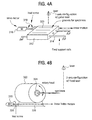
- Figures 4a and 4b are detailed illustrations of two types of indexing devices 306.
- the indexing device 306 comprises a moveable stage 312, fixed support rails 314 upon which the stage 312 moves, and a motor 316 connected to the stage 312 by a lead screw 318.
- the stage 312 comprises one or more grooves 320 to hold the test specimens.
- Figure 4b illustrates an alternate exemplary embodiment and is described in detail subsequently.
- Figure 5a and 5b illustrate tubular specimens marked with airbrush techniques.
- Figure 5a is the specimen pre-tensile testing and
- Figure 5b is post-tensile testing.
- Figures 5c and 5d illustrate tubular specimens marked with the present invention.
- the gauge marks are cleaner and finer both pre and post testing.
- SEM microscopy could be used for specimen measurement in addition to traditional light microscopy or magnification techniques.
- This method could be used to improve the tensile testing of non-tubular geometry samples such as wire or bar.
- This method could be used to improve the tensile testing of non-metallic samples such as polymers or ceramics.
- This method could be used to improve the deformation testing of complex multiaxial deformation tested samples such as stamped sheet metal.
- Figure 4b illustrates an alternate exemplary embodiment of an indexing device 306.
- the device 306 comprises a rotary head 322, a clamping mechanism 324 positioned within the rotary head 322 to hold the specimen, a linear stage 326 and a motor 328 connected to the linear stage 321 via a lead screw 330.
- the rotary head 322 includes a motor, not illustrated.
- the specimen under test may be moved linearly and/or rotationally.
- the energy based marking system could also be comprised of a fixed position energy based marking device with a positioning fixture that has at least two axes of motion: a rotary motion and a linear motion. This would allow for the creation of complex gauge mark shapes on the test specimens. For example, a single spiral line may be created rather than a series of lines.
Landscapes
- Physics & Mathematics (AREA)
- General Physics & Mathematics (AREA)
- Investigating Strength Of Materials By Application Of Mechanical Stress (AREA)
- Length Measuring Devices By Optical Means (AREA)
- Length-Measuring Devices Using Wave Or Particle Radiation (AREA)
- Length Measuring Devices With Unspecified Measuring Means (AREA)
- Laser Beam Processing (AREA)
- Analysing Materials By The Use Of Radiation (AREA)
Abstract
Description
- The present invention relates to a process and device for improving measurement capabilities, and more particularly to a process and device for marking and measuring test specimens in order to determine the deformation properties of the test specimen, including the measurement of macro and micro deformations in the test specimens.
- Currently utilized deformation measurement techniques, as illustrated in Figure 1, utilize an airbrush and stencil marking system in order to create a series of spaced reference marks of known separation on the specimen to be tested. The distance between these marks is referred to as the gauge length and each mark is referred to as a gauge mark.
- Prior methods for marking test specimens, such as sheets, bars and tubes for deformation testing such as tensile testing and elongation testing measurement have a number of drawbacks. For example, certain marking techniques, such as chemical etching and mechanical scratching, may actually alter the surface of the sample to the point where premature failures are induced, thus the test preparation negatively impacts test results. In addition, common marking techniques used to avoid surface damage, such as spray painting, produce marks which may have poorly defined edges, which may reduce the repeatability and precision of measurements, and due to this the minimum spacing of the marks is limited. In addition, these types of marks may be difficult to visualize because of a lack of contrast.
- The present invention overcomes the difficulties associated with currently utilized processes and devices as briefly described above.
- In accordance with a first aspect, the present invention is directed to a method for measuring deformations in test specimens. The method comprises marking at least one test specimen with one or more high resolution gauge marks, deforming the at least one test specimen, and measuring a positional change between the one or more high resolution gauge marks.
- In accordance with another aspect, the present invention is directed to a system for marking test specimens. The system comprises an indexing fixture configured to hold and position one or more test specimens, and an energy source, positioned proximate the indexing fixture, for producing high resolution markings on the one or more test specimens.
- In accordance with another aspect, the present invention is directed to a test specimen comprising at least one high resolution gauge mark.
- The present invention utilizes an energy based device such as a laser to create fine lines, or other fiducial delineations or gauge marks for measurement taking. Due to the precise control available from the laser marking system of the present invention, the energy delivered to the specimen surface may be controlled to the degree that premature failures at the marking points are significantly reduced or eliminated. The presently described system accomplishes this through the production of marks which impact the sample's surface to no more than one half the grain size of the test specimen, for polycrystalline materials. The laser marks are extremely well defined with precise edges and narrow total width, for example, less than one thousandth of an inch so that they may be more precisely measured for post-test gauge lengths and spaced more tightly. With the appropriate laser, total widths of less than ten microns may be achieved.
- The present invention is directed to a novel method for improving the determination of elongation (i.e., strain carrying) capability of tubular or other shaped test specimens. In order to determine elongation of a material being tensile tested, a change in gauge length from the pre-tensile tested to the post-tensile tested state needs to be measured. Strain is defined as the change in length of the specimen divided by the original length of the specimen. This relationship may be formulaically represented as

where E is strain, dL is change in length, and Lo is original specimen length. - The present invention discloses a method for marking test samples via a laser marking device which produces extremely fine, well-defined marks which facilitate more accurate gauge length measurement and tighter/smaller spacing of the gauge marks.
- In accordance with the present invention the test specimen, for example, a tube is placed under the laser marking system (a commercially available galvo device such as the Rofin EasyMark) on a fixture long enough to support the entire length of the sample. A one axis, servo or stepper motor controlled platform moves the tube underneath the laser head in a direction aligned with the tube sample's primary axis (the indexing direction). The index distance is based on the desired gauge length. The laser can image in two axes that allows it to place the marks transverse to the axis of the tube and indexing motion that produces a gauge length mark of suitable quality for measurement and appropriate spacing.
- The present invention is directed to a methodology and system for accurately marking specimens to be tested. The methodology and system may utilize any number of marking techniques, any number of energy based marking devices capable of producing high resolution gauge marks and any number of measuring devices on a multitude of test specimens of varying size, shape, and composition. For ease of explanation, however, an exemplary embodiment is described with respect to a metallic tubular structure suitable for the manufacture of intravascular devices such as stents. In addition, although any type of marking device may be utilized, the exemplary embodiment is described with a laser as the marking device.
- The present invention utilizes an energy based device such as a laser to create fine line delineations or gauge marks for measurement taking. Due to the precise control available from the laser marking system, the energy delivered to the specimen surface may be controlled to the degree that premature failures at the marking points are significantly reduced or eliminated. The laser marks are extremely well-defined with precise edges and narrow total width, for example, less than 0.003 mm (one thousandth of an inch) so that they may be more precisely measured for post-test gauge lengths and spaced more tightly. With the appropriate laser, widths of less than 10 µm (ten microns) may be achieved.
- High resolution marking and spacing is what truly makes this improved measurement method valuable. For small diameter, thin walled tubes, a significant portion of the plastic deformation that occurs during tensile testing happens over a very short (as measured in the tube-axial direction) distance (< 3.18 mm (0.125 inches)). If gauge marks are placed too far apart, the change in length of the specimen due to this necking elongation is not captured during typical elongation measurement. Instead what is measured is the bulk elongation of the material. Since most devices made from thin walled metal tube contain dimensions well under this length scale (typically in the 0.051 - 0.254 mm (0.002 - 0.010 inch) size range), accurately capturing the maximum elongation possible from the material at this scale is critical for proper characterization of the material and device.
- For plastically deformable devices like stents, higher elongation capability is desirable, since it allows for more expansion of a device to accommodate clinicians' needs without device failure. If the elongation capability of the material at this length scale is not known during device design, overly conservative assumptions based on the bulk elongation properties of the material must be used in device design and analysis, which leads to lower performing designs (e.g. lesser stent crimping and overexpansion capability).
- It has been shown through experimentation (at 203 mm, 51 mm and 6.35 mm (8 inches, 2 inches, and ¼ inch) gauge lengths) and extrapolation that as the gauge length spacing becomes smaller (and better scaled to capture the necking elongation of the test sample), that the actual measured elongation will increase. Figure 2 illustrates a plot of elongation increase trend. One can see that as gauge length gets smaller the increase in elongation measured can be dramatic as more of the necking strain is captured. Thus, the value of the present invention becomes clear. The present invention allows for both lower measurement noise/error (due to finer more controlled marks), and more tightly spaced gauge marks, which allows for smaller gauge lengths.
- Therefore, the present invention enables the direct quantification and documentation of higher elongation capabilities for material configurations than has previously been possible. This allows for higher performing stent designs (or other plastically deformable devices) to be created.
- In addition, by use of the precision laser illumination source, a thermodynamically stable oxide may be grown from the native surface when the marking is conducted within an oxidative environment. Intrinsic to the nature of thin ceramic films that are grown from the base material, the resultant oxide film will be strongly adherent to the interfacial (i.e. material to oxide) basal plane. As the surface evolves under applied long-range stress (e.g. that induced under a uniaxial state by the tensile tester), the marked surface grains (i.e. discrete monocrystallographic structures that combine to form the overall polycrystalline tube) slide, rotate and/or deform to provide a form of structural stress relief. The present invention provides for a tenaciously adherent surface marking to be attached to each of these discrete surface grains thereby providing for accurate determination of surface grains both on a macro (or long-range) basis to track overall and modestly localized strains between the principal gage marks. In addition, the individualized marking of each discrete grain provides for the opportunity to track localized surface strains on the granular level so as to provide a meso to micro perspective when evaluating imparted deformation to the tube and/or specimen under test.
- In accordance with the present invention, the test specimens may be coated with any number of suitable coating materials that serve a number of functions. For example, the test specimens to be measured may be coated with a material that creates an optimal ablation environment so that the energy from the energy source (laser) does not heat the base material comprising the test specimen while creating or cutting the gauge marks or delineations. In other words, by judicious selection of a coating material and/or control over the energy source (frequency, amplitude, power) gauge marks or other delineations may be made in the coating material which absorbs the energy from the energy source with minimal transmission to the underlying base material comprising the test specimen, thereby shielding the base material from any deleterious effects that may be produced by the energy source. One such coating material or layer is the oxide layer described above.
- In addition to utilizing any suitable coating, any suitable coating technique may be utilized to apply the coating material to the base test specimen. For example, depending upon the base material, the coating material and the derived thickness of the coating, the coating material may be applied utilizing any number of well known techniques including airbrush spray painting, anodizing and/or dip coating. The depth or thickness of the coating is an important factor as is explained in detail subsequently. Regardless of the coating material and the coating application process, it is important that the coating be a conformal coating that moves with the base material comprising the test specimen on both the macro and microscopic scale such that as the base material is manipulated or deformed, the coating deforms in a manner as precisely as the underlying base material. For example, if the test specimen is stretched a predetermined distance, then the coating should stretch the same predetermined distance so that the measurements are accurate. Typical conformal coatings include Parylene, silicone, acrylic, urethane and epoxy.
- In a slight variation, the energy source may be utilized to bond the coating material to the surface of the base material comprising the test specimen at the points of demarcation or delineation while the portions not exposed to the energy source may be removed utilizing a particular solvent. In this particular variation, raised guage marks or delineations are formed utilizing energy based bonding. This variation results in an embossed surface. This particular variation is similar to the creation of semiconductor mask works utilizing photoresist and is well known in the semiconductor fabrication art.
- In addition to the coating being conformal, it is preferable that the coating material be a material that is in stark contrast to the underlying base material comprising the test specimen, or at least becomes a color or texture that is in stark contrast to the base material when exposed to the energy source. A stark contrast will make it easier to read and/or measure the delineations.
- If no coating is utilized, the energy source may be utilized in the production of gauge marks which impact the test specimen's surface to no more than one half the grain size of the test specimen for polycrystalline materials. If a laser is utilized as the energy source, the laser marks are extremely well defined with precise edges and narrow total widths, for example, less than one thousandth of an inch so that they may be more precisely measured for post-test gauge length and spaced more tightly. Obviously, the closer the spacing, the more precise the measurement. With the appropriate laser and optics, total widths of less than 10 µm (ten microns) may be achieved. In other words, ultra high resolution gauge marks may be formed with a width of no lesser than the frequency of the energy source to create the gauge marks or delineations, which may be less than ten microns, for example, on the order of about 2 µm (two microns). The higher the resolution of the energy source, the higher degree of control over the size and shapes of the marks. It is important to note that this applies to coated as well as non-coated surfaces; however; non-coated or uncoated surfaces are subject to potential deleterious effects as described herein.
- While the width and spacing of the gauge marks or delineations are important, the depth of the gauge marks or delineations are also important. The less invasive the gauge mark, the less likely is the gauge mark to change the characteristics of the underlying base material and thus lessen its impact on the test results. Accordingly, while controlling the depth as described herein is important, the use of coatings as described above may lessen the impact of potential base material surface modifications. In other words, the use of coatings may result in substantially no possibility of altering the characteristics of the underlying base material. For example, in one exemplary embodiment, the energy source may be set to cut or ablate to a depth equal to that of the coating material such that the underlying test specimen surface is exposed but not touched. Alternately, the energy source may be set to cut or ablate to a depth only partially through the coating material, thereby, creating a mark or delineation in the coating material only. In yet another alternate embodiment, the energy source may be set to cut or ablate through the coating material and just into the surface of the underlying test specimen. While the surface of the test specimen is marked, it is to a much less extent than what would be required in a non-coated test specimen. As is seen, the depth of a coated or uncoated test specimen may be varied to suit a particular need. The depth of cut depends on a number of factors, including the underlying material, the coating material and the energy source.
- Embodiments of the invention will now be described by way of example with reference to the accompanying drawings, in which:
- Figure 1 is a diagrammatic representation of a prior art system for marking test specimens.
- Figure 2 is a graphical illustration of strain capability versus gauge length in accordance with the present invention.
- Figure 3 is a diagrammatic representation of a system for marking in accordance with the present invention.
- Figure 4a is a diagrammatic representation of a first exemplary indexing device in accordance with the present invention.
- Figure 4b is a diagrammatic representation of a second exemplary indexing device in accordance with the present invention.
- Figure 5a is an image of a tubular specimen with airbrush gauge marks prior to testing.
- Figure 5b is an image of the tubular specimen of Figure 5a after testing.
- Figure 5c is an image of a tubular specimen with gauge marks made in accordance with the present invention prior to testing.
- Figure 5d is an image of the tubular specimen of Figure 5c after testing.
- Referring to Figure 3, there is illustrated an
exemplary system 300 in accordance with the present invention. Thesystem 300 comprises an energy based markingdevice 302, such as a laser, an energy directing/focusingapparatus 304, such as a lens and mirror arrangement, and anindexing device 306, such as a servo motor driven linear stage fitted with grooves and clamps to hold test specimens. Also illustrated is aspecimen 308 with gauge marks 310 produced by thelaser 302. Figures 4a and 4b are detailed illustrations of two types ofindexing devices 306. In a first exemplary embodiment, illustrated in Figure 4a, theindexing device 306 comprises amoveable stage 312, fixed support rails 314 upon which thestage 312 moves, and amotor 316 connected to thestage 312 by alead screw 318. Thestage 312 comprises one ormore grooves 320 to hold the test specimens. Figure 4b illustrates an alternate exemplary embodiment and is described in detail subsequently. - Figure 5a and 5b illustrate tubular specimens marked with airbrush techniques. Figure 5a is the specimen pre-tensile testing and Figure 5b is post-tensile testing. As can be seen there is a substantial difference between the gauge marks. Figures 5c and 5d illustrate tubular specimens marked with the present invention. As can be seen, the gauge marks are cleaner and finer both pre and post testing.
- To facilitate measurement of extremely small gauge length marks (which is possible with present invention), SEM microscopy could be used for specimen measurement in addition to traditional light microscopy or magnification techniques.
- This method could be used to improve the tensile testing of non-tubular geometry samples such as wire or bar.
- This method could be used to improve the tensile testing of non-metallic samples such as polymers or ceramics.
- This method could be used to improve the deformation testing of complex multiaxial deformation tested samples such as stamped sheet metal.
- Figure 4b illustrates an alternate exemplary embodiment of an
indexing device 306. In this exemplary embodiment, thedevice 306 comprises arotary head 322, aclamping mechanism 324 positioned within therotary head 322 to hold the specimen, alinear stage 326 and a motor 328 connected to the linear stage 321 via alead screw 330. Therotary head 322 includes a motor, not illustrated. In this exemplary embodiment, the specimen under test may be moved linearly and/or rotationally. In other words, the energy based marking system could also be comprised of a fixed position energy based marking device with a positioning fixture that has at least two axes of motion: a rotary motion and a linear motion. This would allow for the creation of complex gauge mark shapes on the test specimens. For example, a single spiral line may be created rather than a series of lines.
Claims (15)
- A method for measuring deformations in test specimens comprising:marking at least one test specimen with one or more high resolution gauge marks;deforming the at least one test specimen; andmeasuring a positional change between the one or more high resolution gauge marks.
- A system for marking test specimens comprising:an indexing fixture configured to hold and position one or more test specimens; andan energy source, positioned proximate the indexing fixture, for producing high resolution markings on the one or more test specimens.
- A test specimen comprising at least one high resolution gauge mark.
- A method for measuring deformations in test specimens comprising:marking at least one test specimen with one or more gauge marks utilizing electromagnetic energy, the gauge marks having a width greater than or equal to a frequency of the electromagnetic energy;deforming the at least one test specimen; andmeasuring a positional change between the one or more gauge marks.
- A method for measuring deformations in test specimens comprising:coating at least one test specimen with a coating material;marking the at least one test specimen with one or more gauge marks utilizing electromagnetic energy, the gauge marks having a width greater than or equal to a frequency of the electromagnetic energy;deforming the at least one test specimen; andmeasuring a positional change between the one or more gauge marks.
- The method for measuring deformations in test specimens according to Claim 5, wherein the depth of the one or more gauge marks is less than a thickness of the coating material.
- The method for measuring deformations in test specimens according to Claim 5, wherein the depth of the one or more gauge marks is equal to a thickness of the coating material.
- The method for measuring deformations in test specimens according to Claim 5, wherein the depth of the one or more gauge marks is greater than a thickness of the coating material.
- A method for measuring deformations in the specimens comprising:marking at least one test specimen with one or more gauge marks utilizing electromagnetic energy, the gauge marks having a spacing equal to or greater than the frequency of the electromagnetic energy;deforming the at least one test specimen; andmeasuring a positional change between the one or more gauge marks.
- A method for measuring deformations in the specimens comprising:coating at least one test specimen with a coating material;marking the at least one test specimen with one or more gauge marks utilizing electromagnetic energy, the gauge marks having a spacing equal to or greater than the frequency of the electromagnetic energy;deforming the at least one test specimen; andmeasuring a positional change between the one or more gauge marks.
- A method for measuring deformations in test specimens comprising:marking at least one test specimen with one or more gauge marks utilizing electromagnetic energy, the gauge markings having a depth of less than or equal to one half the grain size of the material comprising the test specimen;deforming the at least one test specimen; andmeasuring a positional change between the one or more gauge marks.
- A method for measuring deformations in test specimens comprising:coating at least one test specimen with a coating material;marking the at least one test specimen with one or more gauge marks utilizing electromagnetic energy, the gauge markings having a depth of less than or equal to one half the grain size of the material comprising the test specimen;deforming the at least one test specimen; andmeasuring a positional change between the one or more gauge marks.
- A system for marking test specimens comprising:an indexing feature configured to hold and position one or more test specimens; andan energy source positioned proximate the indexing fixture for producing gauge markings having a width greater than or equal to a frequency of the output of the energy source on the one or more test specimens.
- A system for marking test specimens comprising:an indexing feature configured to hold and position one or more test specimens; andan energy source positioned proximate the indexing fixture for producing gauge markings having a spacing equal to or greater than a frequency of the output of the energy source on the one or more test specimens.
- A system for marking test specimens comprising:an indexing feature configured to hold and position one or more test specimens; andan energy source positioned proximate the indexing fixture for producing gauge markings having a depth of less than or equal to one half the grain size of the material comprising the test specimen on the one or more test specimens.
Applications Claiming Priority (2)
| Application Number | Priority Date | Filing Date | Title |
|---|---|---|---|
| US67684805P | 2005-05-02 | 2005-05-02 | |
| US11/410,180 US20070277619A1 (en) | 2005-05-02 | 2006-04-24 | Method for measuring deformations in test specimens and a system for marking the test specimens |
Publications (2)
| Publication Number | Publication Date |
|---|---|
| EP1719972A1 true EP1719972A1 (en) | 2006-11-08 |
| EP1719972B1 EP1719972B1 (en) | 2009-03-18 |
Family
ID=36649753
Family Applications (1)
| Application Number | Title | Priority Date | Filing Date |
|---|---|---|---|
| EP06252281A Expired - Lifetime EP1719972B1 (en) | 2005-05-02 | 2006-04-28 | A method for measuring deformations in test specimens |
Country Status (5)
| Country | Link |
|---|---|
| US (1) | US20070277619A1 (en) |
| EP (1) | EP1719972B1 (en) |
| JP (1) | JP2006337360A (en) |
| AT (1) | ATE426143T1 (en) |
| DE (1) | DE602006005733D1 (en) |
Cited By (3)
| Publication number | Priority date | Publication date | Assignee | Title |
|---|---|---|---|---|
| CN106644704A (en) * | 2017-03-09 | 2017-05-10 | 中国工程物理研究院核物理与化学研究所 | Testing method for microscopic deformation of material |
| RU2658110C1 (en) * | 2017-04-07 | 2018-06-19 | федеральное государственное автономное образовательное учреждение высшего образования "Санкт-Петербургский национальный исследовательский университет информационных технологий, механики и оптики" (Университет ИТМО) | Device for monitoring deformations of structures and facilities of large area |
| CN114964076A (en) * | 2021-08-31 | 2022-08-30 | 中国科学院金属研究所 | Control method for dimensional accuracy and structure uniformity of alloy pipe |
Families Citing this family (7)
| Publication number | Priority date | Publication date | Assignee | Title |
|---|---|---|---|---|
| US7363821B2 (en) * | 2006-08-28 | 2008-04-29 | Cordis Corporation | Systems and methods for fatigue testing stents |
| JP4658175B2 (en) * | 2008-09-30 | 2011-03-23 | ツバキ山久チエイン株式会社 | Load measuring device |
| JP2016061602A (en) * | 2014-09-16 | 2016-04-25 | 国立研究開発法人物質・材料研究機構 | Deformation measuring device of structure and deformation measuring method |
| JP6217603B2 (en) | 2014-11-21 | 2017-10-25 | ブラザー工業株式会社 | Laser marker data creation device |
| US20180120096A1 (en) * | 2015-08-24 | 2018-05-03 | Aerojet Rocketdyne, Inc. | Process for non-destructive testing using direct strain imaging |
| US10228237B2 (en) * | 2017-07-12 | 2019-03-12 | The Boeing Company | Non-destructive optical method for determining minimum bond strength and proving bond efficacy |
| CN110793849A (en) * | 2019-10-12 | 2020-02-14 | 中国直升机设计研究所 | Tool for measuring size of metal sample after stretching |
Citations (6)
| Publication number | Priority date | Publication date | Assignee | Title |
|---|---|---|---|---|
| US3628866A (en) * | 1969-01-24 | 1971-12-21 | Bendix Corp | Noncontacting method of measuring strain |
| DE3042650A1 (en) * | 1979-11-16 | 1981-05-27 | Elesta AG Elektronik, 7310 Bad Ragaz | METHOD AND DEVICE FOR PRODUCING OPTICAL RULES AND SCALE PRODUCED BY THE METHOD |
| EP0727640A2 (en) * | 1995-02-15 | 1996-08-21 | Hewlett-Packard Company | Optical distance measurement |
| EP0843157A2 (en) * | 1996-11-14 | 1998-05-20 | CISE S.p.A. | Method for in-field measurement of permanent deformations on plant components, and assembly of instruments for performing said method |
| WO2001054854A1 (en) * | 2000-01-28 | 2001-08-02 | Gsi Lumonics, Inc. | Laser scanning method and system for marking articles such as printed circuit boards, integrated circuits and the like |
| US20050079499A1 (en) * | 2001-11-15 | 2005-04-14 | Ellin Alexander David Scott | Substrate treatment device and method and encoder scale treated by this method |
Family Cites Families (6)
| Publication number | Priority date | Publication date | Assignee | Title |
|---|---|---|---|---|
| US4547649A (en) * | 1983-03-04 | 1985-10-15 | The Babcock & Wilcox Company | Method for superficial marking of zirconium and certain other metals |
| JP2692599B2 (en) * | 1994-07-27 | 1997-12-17 | 株式会社島津製作所 | Laser non-contact extensometer |
| US6478861B1 (en) * | 1999-06-25 | 2002-11-12 | Videojet Technologies Inc. | Laser markable coating |
| KR100573755B1 (en) * | 2001-05-28 | 2006-04-24 | 마츠시다 덴코 가부시키가이샤 | razor blade |
| US20070098900A1 (en) * | 2004-11-05 | 2007-05-03 | Fuji Hunt Photographic Chemicals, Inc. | Media providing non-contacting formation of high contrast marks and method of using same, composition for forming a laser-markable coating, a laser-markable material and process of forming a marking |
| US7377181B2 (en) * | 2006-03-10 | 2008-05-27 | Northrop Grumman Corporation | In-situ large area optical strain measurement using an encoded dot pattern |
-
2006
- 2006-04-24 US US11/410,180 patent/US20070277619A1/en not_active Abandoned
- 2006-04-28 EP EP06252281A patent/EP1719972B1/en not_active Expired - Lifetime
- 2006-04-28 AT AT06252281T patent/ATE426143T1/en not_active IP Right Cessation
- 2006-04-28 DE DE602006005733T patent/DE602006005733D1/en not_active Expired - Lifetime
- 2006-05-01 JP JP2006127735A patent/JP2006337360A/en not_active Abandoned
Patent Citations (6)
| Publication number | Priority date | Publication date | Assignee | Title |
|---|---|---|---|---|
| US3628866A (en) * | 1969-01-24 | 1971-12-21 | Bendix Corp | Noncontacting method of measuring strain |
| DE3042650A1 (en) * | 1979-11-16 | 1981-05-27 | Elesta AG Elektronik, 7310 Bad Ragaz | METHOD AND DEVICE FOR PRODUCING OPTICAL RULES AND SCALE PRODUCED BY THE METHOD |
| EP0727640A2 (en) * | 1995-02-15 | 1996-08-21 | Hewlett-Packard Company | Optical distance measurement |
| EP0843157A2 (en) * | 1996-11-14 | 1998-05-20 | CISE S.p.A. | Method for in-field measurement of permanent deformations on plant components, and assembly of instruments for performing said method |
| WO2001054854A1 (en) * | 2000-01-28 | 2001-08-02 | Gsi Lumonics, Inc. | Laser scanning method and system for marking articles such as printed circuit boards, integrated circuits and the like |
| US20050079499A1 (en) * | 2001-11-15 | 2005-04-14 | Ellin Alexander David Scott | Substrate treatment device and method and encoder scale treated by this method |
Cited By (4)
| Publication number | Priority date | Publication date | Assignee | Title |
|---|---|---|---|---|
| CN106644704A (en) * | 2017-03-09 | 2017-05-10 | 中国工程物理研究院核物理与化学研究所 | Testing method for microscopic deformation of material |
| CN106644704B (en) * | 2017-03-09 | 2019-02-22 | 中国工程物理研究院核物理与化学研究所 | A test method for microscopic deformation of materials |
| RU2658110C1 (en) * | 2017-04-07 | 2018-06-19 | федеральное государственное автономное образовательное учреждение высшего образования "Санкт-Петербургский национальный исследовательский университет информационных технологий, механики и оптики" (Университет ИТМО) | Device for monitoring deformations of structures and facilities of large area |
| CN114964076A (en) * | 2021-08-31 | 2022-08-30 | 中国科学院金属研究所 | Control method for dimensional accuracy and structure uniformity of alloy pipe |
Also Published As
| Publication number | Publication date |
|---|---|
| EP1719972B1 (en) | 2009-03-18 |
| ATE426143T1 (en) | 2009-04-15 |
| US20070277619A1 (en) | 2007-12-06 |
| DE602006005733D1 (en) | 2009-04-30 |
| JP2006337360A (en) | 2006-12-14 |
Similar Documents
| Publication | Publication Date | Title |
|---|---|---|
| Sharpe et al. | Effect of specimen size on Young's modulus and fracture strength of polysilicon | |
| Jin et al. | Micro-scale deformation measurement using the digital image correlation technique and scanning electron microscope imaging | |
| EP1719972B1 (en) | A method for measuring deformations in test specimens | |
| US20180024035A1 (en) | Apparatus for In-Line Testing and Surface Analysis on a Mechanical Property Tester | |
| US6755075B2 (en) | Ultra micro indentation testing apparatus | |
| CN102261894B (en) | Material deformation measurement method and device based on laser marking automatic tracking | |
| Zhu et al. | On-machine measurement of a slow slide servo diamond-machined 3D microstructure with a curved substrate | |
| US6762846B1 (en) | Substrate surface profile and stress measurement | |
| CN116884872A (en) | Wafer surface curvature radius detection device and method and film stress detection method | |
| EP2467672B1 (en) | Surface alignment and positioning method and apparatus | |
| US20170067735A1 (en) | Apparatus for In-Line Test and Surface Analysis on a Mechanical Property Tester | |
| CN119000642A (en) | Solid material performance integrated test system and test method thereof | |
| KR20180094152A (en) | Measuring form changes of a substrate | |
| CN112067462A (en) | Method and device for prefabricating cracks on ultrathin brittle material | |
| EP4609972A2 (en) | Systems and methods for laser processing system characterization and calibration | |
| CA2545242A1 (en) | A method for measuring deformations in test specimens and a system for marking the test specimines | |
| CN2890890Y (en) | Micro-nanometer scale mechanical property tester | |
| Crosby | Combinatorial characterization of polymer adhesion | |
| CN219996130U (en) | Quick scanning system | |
| Blug et al. | GPU-based digital image correlation system for real-time strain-controlled fatigue and strain field measurement | |
| KR20090044134A (en) | 4-point bending device for X-ray diffraction and thin film stress-strain measurement method using the device | |
| US7458254B2 (en) | Apparatus for evaluating piezoelectric film, and method for evaluating piezoelectric film | |
| DE102004022750B4 (en) | Method for producing a micro test piece | |
| WO2005116716A1 (en) | A means for calibrating a microscope, a method of preparing the means and a method of calibrating a microscope | |
| Albertazzi Jr et al. | Portable residual stresses measurement device using ESPI and a radial in-plane interferometer |
Legal Events
| Date | Code | Title | Description |
|---|---|---|---|
| PUAI | Public reference made under article 153(3) epc to a published international application that has entered the european phase |
Free format text: ORIGINAL CODE: 0009012 |
|
| AK | Designated contracting states |
Kind code of ref document: A1 Designated state(s): AT BE BG CH CY CZ DE DK EE ES FI FR GB GR HU IE IS IT LI LT LU LV MC NL PL PT RO SE SI SK TR |
|
| AX | Request for extension of the european patent |
Extension state: AL BA HR MK YU |
|
| 17P | Request for examination filed |
Effective date: 20070412 |
|
| AKX | Designation fees paid |
Designated state(s): AT BE BG CH CY CZ DE DK EE ES FI FR GB GR HU IE IS IT LI LT LU LV MC NL PL PT RO SE SI SK TR |
|
| 17Q | First examination report despatched |
Effective date: 20080826 |
|
| GRAP | Despatch of communication of intention to grant a patent |
Free format text: ORIGINAL CODE: EPIDOSNIGR1 |
|
| RTI1 | Title (correction) |
Free format text: A METHOD FOR MEASURING DEFORMATIONS IN TEST SPECIMENS |
|
| GRAS | Grant fee paid |
Free format text: ORIGINAL CODE: EPIDOSNIGR3 |
|
| GRAA | (expected) grant |
Free format text: ORIGINAL CODE: 0009210 |
|
| AK | Designated contracting states |
Kind code of ref document: B1 Designated state(s): AT BE BG CH CY CZ DE DK EE ES FI FR GB GR HU IE IS IT LI LT LU LV MC NL PL PT RO SE SI SK TR |
|
| REG | Reference to a national code |
Ref country code: GB Ref legal event code: FG4D |
|
| REG | Reference to a national code |
Ref country code: CH Ref legal event code: EP |
|
| REG | Reference to a national code |
Ref country code: IE Ref legal event code: FG4D |
|
| REF | Corresponds to: |
Ref document number: 602006005733 Country of ref document: DE Date of ref document: 20090430 Kind code of ref document: P |
|
| PG25 | Lapsed in a contracting state [announced via postgrant information from national office to epo] |
Ref country code: SI Free format text: LAPSE BECAUSE OF FAILURE TO SUBMIT A TRANSLATION OF THE DESCRIPTION OR TO PAY THE FEE WITHIN THE PRESCRIBED TIME-LIMIT Effective date: 20090318 Ref country code: LT Free format text: LAPSE BECAUSE OF FAILURE TO SUBMIT A TRANSLATION OF THE DESCRIPTION OR TO PAY THE FEE WITHIN THE PRESCRIBED TIME-LIMIT Effective date: 20090318 Ref country code: FI Free format text: LAPSE BECAUSE OF FAILURE TO SUBMIT A TRANSLATION OF THE DESCRIPTION OR TO PAY THE FEE WITHIN THE PRESCRIBED TIME-LIMIT Effective date: 20090318 |
|
| PG25 | Lapsed in a contracting state [announced via postgrant information from national office to epo] |
Ref country code: AT Free format text: LAPSE BECAUSE OF FAILURE TO SUBMIT A TRANSLATION OF THE DESCRIPTION OR TO PAY THE FEE WITHIN THE PRESCRIBED TIME-LIMIT Effective date: 20090318 Ref country code: PL Free format text: LAPSE BECAUSE OF FAILURE TO SUBMIT A TRANSLATION OF THE DESCRIPTION OR TO PAY THE FEE WITHIN THE PRESCRIBED TIME-LIMIT Effective date: 20090318 Ref country code: LV Free format text: LAPSE BECAUSE OF FAILURE TO SUBMIT A TRANSLATION OF THE DESCRIPTION OR TO PAY THE FEE WITHIN THE PRESCRIBED TIME-LIMIT Effective date: 20090318 Ref country code: SE Free format text: LAPSE BECAUSE OF FAILURE TO SUBMIT A TRANSLATION OF THE DESCRIPTION OR TO PAY THE FEE WITHIN THE PRESCRIBED TIME-LIMIT Effective date: 20090618 |
|
| PG25 | Lapsed in a contracting state [announced via postgrant information from national office to epo] |
Ref country code: ES Free format text: LAPSE BECAUSE OF FAILURE TO SUBMIT A TRANSLATION OF THE DESCRIPTION OR TO PAY THE FEE WITHIN THE PRESCRIBED TIME-LIMIT Effective date: 20090629 Ref country code: EE Free format text: LAPSE BECAUSE OF FAILURE TO SUBMIT A TRANSLATION OF THE DESCRIPTION OR TO PAY THE FEE WITHIN THE PRESCRIBED TIME-LIMIT Effective date: 20090318 Ref country code: PT Free format text: LAPSE BECAUSE OF FAILURE TO SUBMIT A TRANSLATION OF THE DESCRIPTION OR TO PAY THE FEE WITHIN THE PRESCRIBED TIME-LIMIT Effective date: 20090826 Ref country code: CZ Free format text: LAPSE BECAUSE OF FAILURE TO SUBMIT A TRANSLATION OF THE DESCRIPTION OR TO PAY THE FEE WITHIN THE PRESCRIBED TIME-LIMIT Effective date: 20090318 |
|
| PG25 | Lapsed in a contracting state [announced via postgrant information from national office to epo] |
Ref country code: SK Free format text: LAPSE BECAUSE OF FAILURE TO SUBMIT A TRANSLATION OF THE DESCRIPTION OR TO PAY THE FEE WITHIN THE PRESCRIBED TIME-LIMIT Effective date: 20090318 Ref country code: RO Free format text: LAPSE BECAUSE OF FAILURE TO SUBMIT A TRANSLATION OF THE DESCRIPTION OR TO PAY THE FEE WITHIN THE PRESCRIBED TIME-LIMIT Effective date: 20090318 Ref country code: IS Free format text: LAPSE BECAUSE OF FAILURE TO SUBMIT A TRANSLATION OF THE DESCRIPTION OR TO PAY THE FEE WITHIN THE PRESCRIBED TIME-LIMIT Effective date: 20090718 |
|
| PLBE | No opposition filed within time limit |
Free format text: ORIGINAL CODE: 0009261 |
|
| STAA | Information on the status of an ep patent application or granted ep patent |
Free format text: STATUS: NO OPPOSITION FILED WITHIN TIME LIMIT |
|
| PG25 | Lapsed in a contracting state [announced via postgrant information from national office to epo] |
Ref country code: DK Free format text: LAPSE BECAUSE OF FAILURE TO SUBMIT A TRANSLATION OF THE DESCRIPTION OR TO PAY THE FEE WITHIN THE PRESCRIBED TIME-LIMIT Effective date: 20090318 Ref country code: BG Free format text: LAPSE BECAUSE OF FAILURE TO SUBMIT A TRANSLATION OF THE DESCRIPTION OR TO PAY THE FEE WITHIN THE PRESCRIBED TIME-LIMIT Effective date: 20090618 |
|
| 26N | No opposition filed |
Effective date: 20091221 |
|
| PG25 | Lapsed in a contracting state [announced via postgrant information from national office to epo] |
Ref country code: MC Free format text: LAPSE BECAUSE OF NON-PAYMENT OF DUE FEES Effective date: 20090430 |
|
| PG25 | Lapsed in a contracting state [announced via postgrant information from national office to epo] |
Ref country code: GR Free format text: LAPSE BECAUSE OF FAILURE TO SUBMIT A TRANSLATION OF THE DESCRIPTION OR TO PAY THE FEE WITHIN THE PRESCRIBED TIME-LIMIT Effective date: 20090619 |
|
| REG | Reference to a national code |
Ref country code: CH Ref legal event code: PL |
|
| PG25 | Lapsed in a contracting state [announced via postgrant information from national office to epo] |
Ref country code: LI Free format text: LAPSE BECAUSE OF NON-PAYMENT OF DUE FEES Effective date: 20100430 Ref country code: CH Free format text: LAPSE BECAUSE OF NON-PAYMENT OF DUE FEES Effective date: 20100430 |
|
| PG25 | Lapsed in a contracting state [announced via postgrant information from national office to epo] |
Ref country code: LU Free format text: LAPSE BECAUSE OF NON-PAYMENT OF DUE FEES Effective date: 20090428 |
|
| PG25 | Lapsed in a contracting state [announced via postgrant information from national office to epo] |
Ref country code: HU Free format text: LAPSE BECAUSE OF FAILURE TO SUBMIT A TRANSLATION OF THE DESCRIPTION OR TO PAY THE FEE WITHIN THE PRESCRIBED TIME-LIMIT Effective date: 20090919 |
|
| PG25 | Lapsed in a contracting state [announced via postgrant information from national office to epo] |
Ref country code: TR Free format text: LAPSE BECAUSE OF FAILURE TO SUBMIT A TRANSLATION OF THE DESCRIPTION OR TO PAY THE FEE WITHIN THE PRESCRIBED TIME-LIMIT Effective date: 20090318 |
|
| PG25 | Lapsed in a contracting state [announced via postgrant information from national office to epo] |
Ref country code: CY Free format text: LAPSE BECAUSE OF FAILURE TO SUBMIT A TRANSLATION OF THE DESCRIPTION OR TO PAY THE FEE WITHIN THE PRESCRIBED TIME-LIMIT Effective date: 20090318 |
|
| REG | Reference to a national code |
Ref country code: FR Ref legal event code: PLFP Year of fee payment: 11 |
|
| REG | Reference to a national code |
Ref country code: FR Ref legal event code: PLFP Year of fee payment: 12 |
|
| REG | Reference to a national code |
Ref country code: FR Ref legal event code: PLFP Year of fee payment: 13 |
|
| PGFP | Annual fee paid to national office [announced via postgrant information from national office to epo] |
Ref country code: IE Payment date: 20230310 Year of fee payment: 18 Ref country code: FR Payment date: 20230309 Year of fee payment: 18 |
|
| PGFP | Annual fee paid to national office [announced via postgrant information from national office to epo] |
Ref country code: IT Payment date: 20230310 Year of fee payment: 18 Ref country code: GB Payment date: 20230309 Year of fee payment: 18 Ref country code: BE Payment date: 20230315 Year of fee payment: 18 |
|
| PGFP | Annual fee paid to national office [announced via postgrant information from national office to epo] |
Ref country code: NL Payment date: 20230314 Year of fee payment: 18 |
|
| PGFP | Annual fee paid to national office [announced via postgrant information from national office to epo] |
Ref country code: DE Payment date: 20230228 Year of fee payment: 18 |
|
| REG | Reference to a national code |
Ref country code: DE Ref legal event code: R119 Ref document number: 602006005733 Country of ref document: DE |
|
| REG | Reference to a national code |
Ref country code: NL Ref legal event code: MM Effective date: 20240501 |
|
| GBPC | Gb: european patent ceased through non-payment of renewal fee |
Effective date: 20240428 |
|
| REG | Reference to a national code |
Ref country code: BE Ref legal event code: MM Effective date: 20240430 |
|
| PG25 | Lapsed in a contracting state [announced via postgrant information from national office to epo] |
Ref country code: DE Free format text: LAPSE BECAUSE OF NON-PAYMENT OF DUE FEES Effective date: 20241105 |
|
| PG25 | Lapsed in a contracting state [announced via postgrant information from national office to epo] |
Ref country code: NL Free format text: LAPSE BECAUSE OF NON-PAYMENT OF DUE FEES Effective date: 20240501 Ref country code: BE Free format text: LAPSE BECAUSE OF NON-PAYMENT OF DUE FEES Effective date: 20240430 |
|
| PG25 | Lapsed in a contracting state [announced via postgrant information from national office to epo] |
Ref country code: GB Free format text: LAPSE BECAUSE OF NON-PAYMENT OF DUE FEES Effective date: 20240428 |
|
| PG25 | Lapsed in a contracting state [announced via postgrant information from national office to epo] |
Ref country code: FR Free format text: LAPSE BECAUSE OF NON-PAYMENT OF DUE FEES Effective date: 20240430 |
|
| PG25 | Lapsed in a contracting state [announced via postgrant information from national office to epo] |
Ref country code: NL Free format text: LAPSE BECAUSE OF NON-PAYMENT OF DUE FEES Effective date: 20240501 Ref country code: GB Free format text: LAPSE BECAUSE OF NON-PAYMENT OF DUE FEES Effective date: 20240428 Ref country code: FR Free format text: LAPSE BECAUSE OF NON-PAYMENT OF DUE FEES Effective date: 20240430 Ref country code: DE Free format text: LAPSE BECAUSE OF NON-PAYMENT OF DUE FEES Effective date: 20241105 Ref country code: BE Free format text: LAPSE BECAUSE OF NON-PAYMENT OF DUE FEES Effective date: 20240430 |
|
| PG25 | Lapsed in a contracting state [announced via postgrant information from national office to epo] |
Ref country code: IE Free format text: LAPSE BECAUSE OF NON-PAYMENT OF DUE FEES Effective date: 20240428 |
|
| PG25 | Lapsed in a contracting state [announced via postgrant information from national office to epo] |
Ref country code: IT Free format text: LAPSE BECAUSE OF NON-PAYMENT OF DUE FEES Effective date: 20240428 |