EP1717869A2 - Stacked photovoltaic apparatus - Google Patents
Stacked photovoltaic apparatus Download PDFInfo
- Publication number
- EP1717869A2 EP1717869A2 EP06252220A EP06252220A EP1717869A2 EP 1717869 A2 EP1717869 A2 EP 1717869A2 EP 06252220 A EP06252220 A EP 06252220A EP 06252220 A EP06252220 A EP 06252220A EP 1717869 A2 EP1717869 A2 EP 1717869A2
- Authority
- EP
- European Patent Office
- Prior art keywords
- layer
- power generation
- generation unit
- refractive index
- photovoltaic apparatus
- Prior art date
- Legal status (The legal status is an assumption and is not a legal conclusion. Google has not performed a legal analysis and makes no representation as to the accuracy of the status listed.)
- Withdrawn
Links
Images


Classifications
-
- H—ELECTRICITY
- H10—SEMICONDUCTOR DEVICES; ELECTRIC SOLID-STATE DEVICES NOT OTHERWISE PROVIDED FOR
- H10F—INORGANIC SEMICONDUCTOR DEVICES SENSITIVE TO INFRARED RADIATION, LIGHT, ELECTROMAGNETIC RADIATION OF SHORTER WAVELENGTH OR CORPUSCULAR RADIATION
- H10F10/00—Individual photovoltaic cells, e.g. solar cells
- H10F10/10—Individual photovoltaic cells, e.g. solar cells having potential barriers
- H10F10/17—Photovoltaic cells having only PIN junction potential barriers
- H10F10/172—Photovoltaic cells having only PIN junction potential barriers comprising multiple PIN junctions, e.g. tandem cells
-
- H—ELECTRICITY
- H10—SEMICONDUCTOR DEVICES; ELECTRIC SOLID-STATE DEVICES NOT OTHERWISE PROVIDED FOR
- H10F—INORGANIC SEMICONDUCTOR DEVICES SENSITIVE TO INFRARED RADIATION, LIGHT, ELECTROMAGNETIC RADIATION OF SHORTER WAVELENGTH OR CORPUSCULAR RADIATION
- H10F77/00—Constructional details of devices covered by this subclass
- H10F77/40—Optical elements or arrangements
- H10F77/42—Optical elements or arrangements directly associated or integrated with photovoltaic cells, e.g. light-reflecting means or light-concentrating means
- H10F77/488—Reflecting light-concentrating means, e.g. parabolic mirrors or concentrators using total internal reflection
-
- Y—GENERAL TAGGING OF NEW TECHNOLOGICAL DEVELOPMENTS; GENERAL TAGGING OF CROSS-SECTIONAL TECHNOLOGIES SPANNING OVER SEVERAL SECTIONS OF THE IPC; TECHNICAL SUBJECTS COVERED BY FORMER USPC CROSS-REFERENCE ART COLLECTIONS [XRACs] AND DIGESTS
- Y02—TECHNOLOGIES OR APPLICATIONS FOR MITIGATION OR ADAPTATION AGAINST CLIMATE CHANGE
- Y02E—REDUCTION OF GREENHOUSE GAS [GHG] EMISSIONS, RELATED TO ENERGY GENERATION, TRANSMISSION OR DISTRIBUTION
- Y02E10/00—Energy generation through renewable energy sources
- Y02E10/50—Photovoltaic [PV] energy
- Y02E10/52—PV systems with concentrators
-
- Y—GENERAL TAGGING OF NEW TECHNOLOGICAL DEVELOPMENTS; GENERAL TAGGING OF CROSS-SECTIONAL TECHNOLOGIES SPANNING OVER SEVERAL SECTIONS OF THE IPC; TECHNICAL SUBJECTS COVERED BY FORMER USPC CROSS-REFERENCE ART COLLECTIONS [XRACs] AND DIGESTS
- Y02—TECHNOLOGIES OR APPLICATIONS FOR MITIGATION OR ADAPTATION AGAINST CLIMATE CHANGE
- Y02E—REDUCTION OF GREENHOUSE GAS [GHG] EMISSIONS, RELATED TO ENERGY GENERATION, TRANSMISSION OR DISTRIBUTION
- Y02E10/00—Energy generation through renewable energy sources
- Y02E10/50—Photovoltaic [PV] energy
- Y02E10/548—Amorphous silicon PV cells
Definitions
- the present invention relates to a stacked photovoltaic apparatus, and more particularly, it relates to a stacked photovoltaic apparatus including a plurality of power generation units.
- a stacked photovoltaic apparatus prepared by successively stacking a first power generation unit, an intermediate layer and a second power generation unit is known in general, as disclosed in Japanese Patent Laying-Open No. 2002-222972 , for example.
- the aforementioned Japanese Patent Laying-Open No. 2002-222972 discloses a stacked photovoltaic apparatus comprising an intermediate layer of ZnO formed between a first power generation unit including a plurality of microcrystalline Si layers and a second power generation unit including a plurality of amorphous Si layers.
- the intermediate layer of ZnO is provided for reflecting light incident from the side of the second power generation unit to pass through the second power generation unit toward the side of the second power generation unit on the interface between the second power generation unit (amorphous Si layers) and the intermediate layer.
- the intermediate layer of ZnO in the aforementioned Japanese Patent Laying-Open No. 2002-222972 is provided for increasing the quantity of light incident upon the second power generation unit, thereby increasing the quantity of light photoelectrically converted in the second power generation unit.
- the difference (1.5) between the refractive index (2.0) of the ZnO layer constituting the intermediate layer and the refractive index (3.5) of the amorphous Si layers constituting the second power generation unit is so small that the quantity of light reflected on the interface between the intermediate layer and the second power generation unit is disadvantageously small despite the intermediate layer of ZnO.
- the rate of increase of the light photoelectrically converted in the second power generation unit is so small that it is difficult to increase the quantity of short-circuit current despite the intermediate layer of ZnO. Consequently, it is difficult to improve the output characteristics of the stacked photovoltaic apparatus.
- the present invention has been proposed in order to solve the aforementioned problem, and an object of the present invention is to provide a stacked photovoltaic apparatus capable of improving the output characteristics.
- a photovoltaic apparatus comprises a first power generation unit including a first semiconductor layer functioning as a photoelectric conversion layer, a second power generation unit including a first conductive type second semiconductor layer formed on the first power generation unit with a first refractive index, a third semiconductor layer of a substantially intrinsic amorphous semiconductor formed on the second semiconductor layer for functioning as another photoelectric conversion layer and a second conductive type fourth semiconductor layer formed on the third semiconductor layer, an intermediate layer formed between the first power generation unit and the second power generation unit with a second refractive index and a reflection promotive layer formed between the intermediate layer and the second semiconductor layer of the second power generation unit with such a third refractive index that the difference between the third refractive index and the first refractive index of the second semiconductor layer is larger than the difference between the second refractive index of the intermediate layer and the first refractive index of the second semiconductor layer.
- the reflection promotive layer having such a third refractive index that the difference between the third refractive index and the first refractive index of the second semiconductor layer is larger than the difference between the second refractive index of the intermediate layer and the first refractive index of the second semiconductor layer is so formed between the intermediate layer and the second semiconductor layer of the second power generation unit that the reflectance on the interface between the reflection promotive layer and the second semiconductor layer of the second power generation unit is higher than that on the interface between the intermediate layer and the second semiconductor layer holding no reflection promotive layer therebetween with respect to light incident from the side of the second power generation unit, whereby the quantity of light reflected toward the side of the second power generation unit can be increased as compared with the case of forming no reflection promotive layer between the intermediate layer and the second semiconductor layer.
- the quantity of light incident upon the third semiconductor layer of the second power generation unit functioning as the photoelectric conversion layer from the side of the second power generation unit can be so increased as to increase the quantity of light photoelectrically converted in the third semiconductor layer (photoelectric conversion layer) of the second power generation unit. Consequently, the quantity of short-circuit current can be so increased as to improve the output characteristics of the stacked photovoltaic apparatus.
- the quantity of light incident upon the third semiconductor layer (photoelectric conversion layer) of the second power generation unit can be increased due to the reflection promotive layer formed between the intermediate layer and the second semiconductor layer of the second power generation unit, whereby the quantity of light photoelectrically converted in the third semiconductor layer (photoelectric conversion layer) is not reduced due to a small optical path length in the third semiconductor layer (photoelectric conversion layer) having a small thickness.
- the thickness of an amorphous Si layer, more easily photo-deteriorated than a microcrystalline Si layer, employed as the third semiconductor layer (photoelectric conversion layer) of the second power generation unit can be so reduced as to suppress photo-deterioration of the amorphous Si layer functioning as the photoelectric conversion layer resulting from a large thickness. Therefore, the rate of photo-deterioration of the output characteristics of the stacked photovoltaic apparatus including the second power generation unit having the photoelectric conversion layer formed by the amorphous Si layer can be inhibited from increase.
- the second refractive index of the intermediate layer is preferably smaller than the first refractive index of the second semiconductor layer
- the third refractive index of the reflection promotive layer is preferably smaller than the second refractive index of the intermediate layer.
- the intermediate layer is preferably formed by a conductive layer
- the reflection promotive layer is preferably formed by an insulator layer with a smaller thickness than the intermediate layer.
- the insulator layer (reflection promotive layer) formed between the intermediate layer and the second semiconductor layer of the second power generation unit with the small thickness can suppress disadvantageous increase of electric resistance between the intermediate layer and the second semiconductor layer.
- the intermediate layer preferably includes a metal oxide layer
- the metal oxide layer constituting the intermediate layer preferably includes a first portion having a first oxygen concentration and a second portion, positioned closer to the reflection promotive layer, having a second oxygen concentration lower than the first oxygen concentration of the first portion.
- the conductivity of the second portion of the intermediate layer having the low second oxygen concentration can be so increased as to increase the total conductivity of the intermediate layer.
- series resistance can be inhibited from increase in the stacked photovoltaic apparatus having the first and second power generation units serially connected with each other through the intermediate layer. Consequently, the fill factor of the stacked photovoltaic apparatus can be so inhibited from reduction that conversion efficiency can be improved.
- the reflection promotive layer preferably includes an oxygen-containing layer, and is preferably formed on the second portion of the metal oxide layer constituting the intermediate layer.
- oxygen escapes from a portion (second portion) around the surface of the intermediate layer (metal oxide layer) closer to the reflection promotive layer and moves toward the reflection promotive layer when the oxygen-containing layer functioning as the reflection promotive layer is formed on the intermediate layer (metal oxide layer) by plasma CVD, for example, whereby the second oxygen concentration of the second portion of the metal oxide layer constituting the intermediate layer can be easily lowered.
- the reflection promotive layer preferably consists of an oxide of an element constituting the second semiconductor layer of the second power generation unit.
- the reflection promotive layer is constituted of SiO 2 having a refractive index of 1.5 when Si having a refractive index of 3.5 is employed as the material for the second semiconductor layer, whereby the difference between the refractive indices of the second semiconductor layer and the reflection promotive layer can be easily increased.
- the element constituting the second semiconductor layer of the second power generation unit is preferably Si.
- the second semiconductor layer is constituted of Si (refractive index: 3.5) and the reflection promotive layer is constituted of SiO 2 (refractive index: 1.5), whereby the difference between the refractive indices of the second semiconductor layer and the reflection promotive layer can be more easily increased.
- the second semiconductor layer preferably includes an Si layer
- the intermediate layer preferably includes a ZnO layer
- the reflection promotive layer preferably includes an SiO 2 layer.
- the first semiconductor layer of the first power generation unit functioning as the photoelectric conversion layer preferably includes a microcrystalline semiconductor layer
- the second power generation unit including the second semiconductor layer of the amorphous semiconductor functioning as the photoelectric conversion layer is preferably arranged on a light incidence side.
- the third semiconductor layer of the second power generation unit functioning as the photoelectric conversion layer preferably photoelectrically converts light incident from the side of the second power generation unit and light reflected toward the side of the third semiconductor layer on the interface between the second semiconductor layer of the second power generation unit and the reflection promotive layer. According to this structure, the quantity of light photoelectrically converted in the third semiconductor layer (photoelectric conversion layer) of the second power generation unit can be easily increased.
- the photoelectric conversion layer of the first power generation unit preferably photoelectrically converts light incident from the side of the second power generation unit and transmitted through the reflection promotive layer. According to this structure, the light incident from the side of the second power generation unit can be easily photoelectrically converted in the photoelectric conversion layer of the first power generation unit.
- the reflection promotive layer preferably has a corrugated surface. According to this structure, the degree of light scattering on the interface between the second semiconductor layer of the second power generation unit and the reflection promotive layer is so increased as to further increase the path length of the light reflected toward the side of the photoelectric conversion layer (third semiconductor layer) of the second power generation unit.
- the second semiconductor layer of the second power generation unit is preferably formed on the corrugated surface of the reflection promotive layer.
- the surface of the second semiconductor layer can be corrugated by reflecting the corrugated surface of the reflection promotive layer, whereby light can be scattered through the corrugated surface of the second semiconductor layer.
- a light confinement effect can be improved in the second power generation unit.
- the photoelectric conversion layer of at least either the first power generation unit or the second power generation unit preferably has a corrugated surface. According to this structure, light can be scattered through the corrugated surface of at least either the first power generation unit or the second power generation unit, whereby a light confinement effect can be improved in at least either the first power generation unit or the second power generation unit.
- the stacked photovoltaic apparatus preferably further comprises a substrate transmitting no light, and the first power generation unit, the intermediate layer, the reflection promotive layer and the second power generation unit are preferably successively stacked on the substrate.
- light photoelectrically converted in the second power generation unit is incident from the side of the second power generation unit, whereby the incident light can be easily reflected toward the third semiconductor layer (photoelectric conversion layer) of the second power generation unit on the interface between the second semiconductor layer of the second power generation unit and the reflection promotive layer.
- a resin layer b of polyimide resin having a thickness of 20 ⁇ m is formed on a planar stainless steel sheet (SUS430) 1a having a thickness of 0.15 mm, as shown in Fig. 1.
- the stainless steel sheet 1a and the resin layer 1b constitute a substrate 1 having a planar surface.
- a planar back electrode 2 of Ag having a thickness of 200 nm is formed on the substrate 1 (resin layer 1b).
- the stacked photovoltaic apparatus according to Example 1 is formed by a microcrystalline Si-based power generation unit 3 and an amorphous Si-based power generation unit 6 stacked with each other, while the amorphous Si-based power generation unit 6 is arranged on a light incidence side.
- the microcrystalline Si-based power generation unit 3 is an example of the "first power generation unit” in the present invention
- the amorphous Si-based power generation unit 6 is an example of the "second power generation unit” in the present invention.
- an n-type layer 31 of n-type microcrystalline Si, a photoelectric conversion layer 32 of non-doped microcrystalline Si and a p-type layer 33 of p-type microcrystalline Si are successively formed on the back electrode 2.
- the n-type layer 31, the photoelectric conversion layer 32 and the p-type layer 33 have thicknesses of 80 nm, 2 ⁇ m and 20 nm respectively.
- the photoelectric conversion layer 32 is an example of the "first semiconductor layer" in the present invention.
- the n-type layer 31, the photoelectric conversion layer 32 and the p-type layer 33 constitute the microcrystalline Si-based power generation unit 3.
- a ZnO layer 4 having a thickness of 20 nm, doped with 2 % of Al is formed on the microcrystalline Si-based power generation unit 3 (p-type layer 33) as an intermediate layer.
- the ZnO layer 4 has different oxygen concentrations in an area 4a closer to the microcrystalline Si-based power generation unit 3 and another area (closer to the amorphous Si-based power generation unit 6) 4b around the surface thereof.
- the area 4b of the ZnO layer 4 around the surface thereof has a lower oxygen concentration than the remaining area 4a of the ZnO layer 4.
- the ZnO layer 4 has a refractive index of 2.0, which is smaller than the refractive index (3.5) of an n-type layer 61 of the amorphous Si-based power generation unit 6 described later.
- the ZnO layer 4 is an example of the "intermediate layer", the "conductive layer” or the “metal oxide layer” in the present invention.
- the areas 4a and 4b are examples of the "first portion” and the "second portion” in the present invention respectively.
- This SiO 2 film 5 has a refractive index of 1.5, which is smaller than the refractive index (2.0) of the ZnO layer 4.
- the difference (2.0) between the refractive index (1.5) of the SiO 2 film 5 and the refractive index (3.5) of the n-type layer 61 of the amorphous Si-based power generation unit 6 is larger than the difference (1.5) between the refractive index (2.0) of the ZnO layer 4 and the refractive index (3.5) of the n-type layer 61 of the amorphous Si-based power generation unit 6.
- the SiO 2 film 5 is an example of the "reflection promotive layer" or the "insulator layer” in the present invention.
- the n-type layer 61 of n-type amorphous Si, a photoelectric conversion layer 62 of non-doped amorphous Si and a p-type layer 63 of p-type amorphous Si are successively formed on the SiO 2 film 5.
- the n-type layer 61, the photoelectric conversion layer 62 and the p-type layer 63 have thicknesses of 20 nm, 350 nm and 15 nm respectively.
- the Si layers constituting the n-type layer 61, the photoelectric conversion layer 62 and the p-type layer 63 respectively have refractive indices of 3.5.
- the n-type layer 61, the photoelectric conversion layer 62 and the p-type layer 63 are examples of the "second semiconductor layer", the “third semiconductor layer” and the “fourth semiconductor layer” in the present invention respectively.
- the n-type layer 61, the photoelectric conversion layer 62 and the p-type layer 63 constitute the amorphous Si-based power generation unit 6.
- a surface transparent electrode 7 of ITO (indium tin oxide) having a thickness of 80 nm is formed on the amorphous Si-based power generation unit 6 (p-type layer 63).
- Collectors 8 of Ag having a thickness of 2 ⁇ m are formed on prescribed regions of the surface transparent electrode 7.
- the substrate 1 constituted of the stainless steel sheet 1a and the resin layer 1b was prepared by vapor-depositing/polymerizing the resin layer 1b of polyimide resin having the thickness of 20 ⁇ m on the planar stainless steel sheet 1a having the thickness of 0.15 mm, as shown in Fig. 1. Thereafter the planar back electrode 2 of Ag having the thickness of 200 nm was formed on the substrate 1 (resin layer 1b) by RF magnetron sputtering.
- the three Si layers constituting the microcrystalline Si-based power generation unit 3 were successively formed on the back electrode 2 by plasma CVD (chemical vapor deposition). More specifically, the n-type layer 31 of n-type microcrystalline Si, the photoelectric conversion layer 32 of non-doped microcrystalline Si and the p-type layer 33 of p-type microcrystalline Si were successively formed. At this time, the n-type layer 31, the photoelectric conversion layer 32 and the p-type layer 33 were formed with the thicknesses of 80 nm, 2 ⁇ m and 20 nm respectively. Table 1 shows the conditions employed for forming the n-type layer 31, the photoelectric conversion layer 32 and the p-type layer 33 respectively.
- the substrate temperature, the reaction pressure and the high-frequency power for forming the n-type layer 31 of n-type microcrystalline Si were set to 160°C, 26 Pa and 100 W respectively. Further, the gas flow rates of SiH 4 gas, H 2 gas and PH 3 gas for forming the n-type layer 31 were set to 3 sccm, 200 sccm and 3 sccm respectively. H 2 -based PH 3 gas containing 2 % of PH 3 was employed as the PH 3 gas.
- the substrate temperature, the reaction pressure and the high-frequency power for forming the photoelectric conversion layer 32 of non-doped microcrystalline Si were set to 200°C, 133 Pa and 30 W respectively. Further, the gas flow rates of SiH 4 gas and H 2 gas for forming the photoelectric conversion layer 32 were set to 20 sccm and 400 sccm respectively.
- the substrate temperature, the reaction pressure and the high-frequency power for forming the p-type layer 33 of p-type microcrystalline Si were set to 120°C, 133 Pa and 50 W respectively. Further, the gas flow rates of SiH 4 gas, H 2 gas and B 2 H 6 gas for forming the p-type layer 33 were set to 1 sccm, 400 sccm and 1 sccm respectively. H 2 -based B 2 H 6 gas containing 1 % of B 2 H 6 was employed as the B 2 H 6 gas.
- the ZnO layer 4 having the refractive index of 2.0 was formed on the microcrystalline Si-based power generation unit 3 (p-type layer 33) as the intermediate layer by RF magnetron sputtering. At this time, the ZnO layer 4 was formed with the thickness of 20 nm. Table 2 shows conditions employed for forming the ZnO layer 4.
- the substrate temperature, the reaction pressure and the high-frequency power for forming the ZnO layer 4 were set to 100°C, 50 Pa and 280 W respectively. Further, the gas flow rate of Ar gas for forming the ZnO layer 4 was set to 10 sccm.
- the SiO 2 film 5 having the refractive index of 1.5 was formed on the ZnO layer 4 as the reflection promotive layer by plasma CVD. At this time, the SiO 2 film 5 was formed with the thickness of 10 nm. Table 3 shows conditions employed for forming the SiO 2 film 5.
- the substrate temperature, the reaction pressure and the high-frequency power for forming the SiO 2 film 5 were set to 180°C, 50 Pa and 30 W respectively. Further, the gas flow rates of SiH 4 gas, H 2 gas and CO 2 gas for forming the SiO 2 film 5 were set to 80 sccm, 160 sccm and 0.8 sccm respectively.
- the three Si layers constituting the amorphous Si-based power generation unit 6 with the refractive indices of 3.5 were successively formed on the SiO 2 film 5 by plasma CVD. More specifically, the n-type layer 61 of n-type amorphous Si, the photoelectric conversion layer 62 of non-doped amorphous Si and the p-type layer 63 of p-type amorphous Si were successively formed. At this time, the n-type layer 61, the photoelectric conversion layer 62 and the p-type layer 63 were formed with the thicknesses of 20 nm, 350 nm and 15 nm respectively. Table 4 shows conditions employed for forming the n-type layer 61, the photoelectric conversion layer 62 and the p-type layer 63 respectively.
- the substrate temperature, the reaction pressure and the high-frequency power for forming the n-type layer 61 of n-type microcrystalline Si were set to 180°C, 50 Pa and 30 W respectively. Further, the gas flow rates of SiH 4 gas, H 2 gas and PH 3 gas for forming the n-type layer 61 were set to 80 sccm, 160 sccm and 80 sccm respectively. H 2 -based PH 3 gas containing 2 % of PH 3 was employed as the PH 3 gas.
- the substrate temperature, the reaction pressure and the high-frequency power for forming the photoelectric conversion layer 62 of non-doped microcrystalline Si were set to 180°C, 130 Pa and 30 W respectively. Further, the gas flow rates of SiH 4 gas and H 2 gas for forming the photoelectric conversion layer 62 were set to 300 sccm and 1000 sccm respectively.
- the substrate temperature, the reaction pressure and the high-frequency power for forming the p-type layer 63 of p-type amorphous Si were set to 90°C, 80 Pa and 30 W respectively. Further, the gas flow rates of SiH 4 gas, H 2 gas and B 2 H 6 gas for forming the p-type layer 63 were set to 40 sccm, 800 sccm and 12 sccm respectively. H 2 -based B 2 H 6 gas containing 1 % of B 2 H 6 was employed as the B 2 H 6 gas.
- the surface transparent electrode 7 of ITO having the thickness of 80 nm was formed on the amorphous Si-based power generation unit 6 (p-type layer 63) by RF magnetron sputtering. Thereafter the collectors 8 of Ag having the thickness of 2 ⁇ m were formed on the prescribed regions of the surface transparent electrode 7 by vacuum evaporation, thereby preparing the stacked photovoltaic apparatus according to Example 1.
- the stacked photovoltaic apparatus according to Example 1 exhibited the energy of 103.5 eV when the intensity on the area corresponding to the SiO 2 film 5 reached the peak (P1 in Fig. 2) as shown in Fig. 2, whereby it has been confirmable that the SiO 2 film 5 was present between the microcrystalline Si-based power generation unit 3 and the amorphous Si-based power generation unit 6.
- the energy observed when the intensity on the area 4b of the ZnO layer 4 around the surface thereof reached the peak (P2 in Fig. 3) is smaller than that observed when the intensity on the remaining area 4a of the ZnO layer 4 reached the peak (P3 in Fig. 3), whereby it has been proved that the oxygen concentration in the area 4b of the ZnO layer 4 around the surface thereof was lower than the oxygen concentration in the remaining area 4a of the ZnO layer 4.
- a substrate 1 was prepared by vapor-depositing/polymerizing a resin layer 1b of polyimide resin having a thickness of 20 ⁇ m on a stainless steel sheet 1a having a thickness of 0.15 mm, similarly to the aforementioned Example 1. Thereafter a back electrode 2 of Ag having a thickness of 200 nm was formed on the substrate 1 by RF magnetron sputtering.
- a microcrystalline Si-based power generation unit 3 consisting of three Si layers was formed on the back electrode 2 by plasma CVD, similarly to the aforementioned Example 1.
- an n-type layer 31 of n-type microcrystalline Si, a photoelectric conversion layer 32 of non-doped microcrystalline Si and a p-type layer 33 of p-type microcrystalline Si were successively formed on the back electrode 2.
- the n-type layer 31, the photoelectric conversion layer 32 and the p-type layer 33 were formed with thicknesses of 80 nm, 2 ⁇ m and 20 nm respectively.
- the n-type layer 31, the photoelectric conversion layer 32 and the p-type layer 33 were formed under the same conditions as those shown in Table 1.
- a ZnO layer 14 having a refractive index of 2.0 was formed on the microcrystalline Si-based power generation unit 3 (p-type layer 33) as an intermediate layer by RF magnetron sputtering.
- the ZnO layer 14 was formed with a thickness of 20 nm, under the same conditions as those shown in Table 2.
- no SiO 2 film was formed on the ZnO layer 14, dissimilarly to the aforementioned Example 1. Therefore, the ZnO layer 14 according to comparative example exhibited a higher oxygen concentration than the ZnO layer 4 according to the aforementioned Example 1 since no O (oxygen) escaped from the ZnO layer 14.
- an n-type layer 61 of n-type amorphous Si, a photoelectric conversion layer 62 of non-doped amorphous Si and a p-type layer 63 of p-type amorphous Si were successively formed on the ZnO layer 14.
- the n-type layer 61, the photoelectric conversion layer 62 and the p-type layer 63 were formed with thicknesses of 20 nm, 350 nm and 15 nm respectively, under the same conditions as those shown in Table 4.
- a surface transparent electrode 7 of ITO having a thickness of 80 nm was formed on the amorphous Si-based power generation unit 6 (p-type layer 63) by RF magnetron sputtering, similarly to the aforementioned Example 1. Further, collectors 8 of Ag having a thickness of 2 ⁇ m were formed on prescribed regions of the surface transparent electrode 7 by vacuum evaporation.
- the stacked photovoltaic apparatus according to comparative example was prepared in this manner. In the stacked photovoltaic apparatus according to comparative example, light is incident from the side of the amorphous Si-based power generation unit 6, similarly to the aforementioned Example 1.
- the stacked photovoltaic apparatus according to Example 1 formed with the SiO 2 film 5 (refractive index: 1.5) between the ZnO layer 4 (refractive index: 2.0) functioning as the intermediate layer and the n-type layer 61 (refractive index: 3.5) of the amorphous Si-based power generation unit 6 formed on the microcrystalline Si-based power generation unit 3 through the intermediate layer exhibited larger short-circuit current than comparative example formed with no SiO 2 film between the ZnO layer 14 (refractive index: 2.0) functioning as the intermediate layer and the n-type layer 61 (refractive index: 3.5). More specifically, the normalized short-circuit current of Example 1 was 1.03.
- Example 1 having the difference of 2.0 between the refractive indices of the n-type layer 61 and the SiO 2 film 5 as compared with comparative example having the difference of 1.5 between the refractive indices of the n-type layer 61 and the ZnO layer 14.
- the quantity of light photoelectrically converted in the photoelectric conversion layer 62 was conceivably more increased in Example 1 as compared with comparative example, due to the large quantity of light incident upon the amorphous Si-based power generation unit 6.
- Example 5 it has also been proved that the fill factor and the conversion efficiency were more improved in the stacked photovoltaic apparatus according to Example 1 having the amorphous Si-based power generation unit 6 provided on the microcrystalline Si-based power generation unit 3 through the intermediate layer formed by the ZnO layer 4 including the area 4b, having the low oxygen concentration, around the surface thereof as compared with the stacked photovoltaic apparatus according to comparative example employing the ZnO layer 14 having the total oxygen concentration higher than the oxygen concentration in the area 4b of the ZnO layer 4 in the stacked photovoltaic apparatus according to Example 1 as the intermediate layer. More specifically, the normalized fill factor and the normalized conversion efficiency of Example 1 were 1.02 and 1.04 respectively.
- Example 1 the open-circuit voltage of the stacked photovoltaic apparatus according to Example 1 was slightly smaller than that of the stacked photovoltaic apparatus according to comparative example 1. More specifically, the normalized open-circuit voltage of Example 1 was 0.99.
- the SiO 2 film 5 having such a refractive index (1.5) that the difference between the same and the refractive index (3.5) of the n-type layer 61 is larger than the difference between the refractive index (2.0) of the ZnO layer 4 and the refractive index (3.5) of the n-type layer 61 is so formed between the ZnO layer 4 functioning as the intermediate layer and the n-type layer 61 of the amorphous Si-based power generation unit 6 that the reflectance on the interface between the SiO 2 film 5 and the n-type layer 61 layer of the amorphous Si-based power generation unit 6 is higher than that on the interface between the ZnO layer 4 and the n-type layer 61 holding no Si0 2 film 5 therebetween with respect to light incident from the side of the amorphous Si-based power generation unit 6, whereby the quantity of light reflected toward the side of the amorphous Si-based power generation unit 6 can be increased as compared with the case of forming no
- the quantity of light incident upon the photoelectric conversion layer 62 of the amorphous Si-based power generation unit 6 can be so increased as to increase the quantity of light photoelectrically converted in the photoelectric conversion layer 62 of the amorphous Si-based power generation unit 6. Consequently, the quantity of short-circuit current can be so increased as to improve the output characteristics of the stacked photovoltaic apparatus.
- the SiO 2 film 5 employed as an insulator layer has the thickness smaller than that of the ZnO layer 5, whereby the SiO 2 film 5 formed between the ZnO layer 4 and the n-type layer 61 of the amorphous Si-based power generation unit 6 with the small thickness can inhibit electric resistance between the ZnO layer 4 and the n-type layer 61 from disadvantageous increase.
- the ZnO layer 4 is employed as the intermediate layer while the oxygen concentration in the area 4b of the ZnO layer 4 around the surface thereof is rendered lower than that in the remaining area 4a of the ZnO layer 4, whereby the conductivity in the area 4b, having the low oxygen concentration, of the ZnO layer 4 around the surface thereof can be so increased as to increase the total conductivity of the ZnO layer 4.
- series resistance can be inhibited from increase in the stacked photovoltaic apparatus having the microcrystalline Si-based power generation unit 3 and the amorphous Si-based power generation unit 6 serially connected with each other through the ZnO layer 4. Consequently, the fill factor of the stacked photovoltaic apparatus can be so inhibited from reduction that the conversion efficiency can be improved.
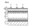
- Fig. 5 is a sectional view showing the structure of a stacked photovoltaic apparatus according to Example 2 of the present invention.
- a photoelectric conversion layer 162 of an amorphous Si-based power generation unit 16 in the stacked photovoltaic apparatus according to Example 2 has a thickness of 300 nm, which is smaller than the thickness (350 nm) of the photoelectric conversion layer 62 of the amorphous Si-based power generation unit 6 according to Example 1 shown in Fig. 1, in a structure similar to that of the stacked photovoltaic apparatus according to the aforementioned Example 1.
- the amorphous Si-based power generation unit 16 is an example of the "second power generation unit” in the present invention
- the photoelectric conversion layer 162 is an example of the "third semiconductor layer” in the present invention.
- the remaining structure of the stacked photovoltaic apparatus according to Example 2 is similar to that of the stacked photovoltaic apparatus according to Example 1.
- an SiO 2 film 5 having a refractive index of 1.5 is formed between a ZnO layer 4 having a refractive index of 2.0 and an n-type layer 61 of the amorphous Si-based power generation unit 16 having a refractive index of 3.5, similarly to the aforementioned Example 1.
- An area 4b of the ZnO layer 4 around the surface thereof has an oxygen concentration lower than that in the remaining area 4a of the ZnO layer 4.
- the stacked photovoltaic apparatus according to Example 2 was prepared through a process similar to that employed for preparing the stacked photovoltaic apparatus according to the aforementioned Example 1. According to Example 2, however, the time for forming the photoelectric conversion layer 162 of the amorphous Si-based power generation unit 16 of amorphous Si was shorter than that for forming the photoelectric conversion layer 62 of the amorphous Si-based power generation unit 6 according to Example 1 shown in Fig. 1. Thus, the photoelectric conversion layer 162 of the amorphous Si-based power generation unit 16 was formed with the thickness (300 nm) smaller than the thickness (350 nm) of the photoelectric conversion layer 62 of the amorphous Si-based power generation unit 6 according to Example 1 shown in Fig. 1.
- the stacked photovoltaic apparatus according to Example 2 prepared by setting the photoelectric conversion layer 162 of the amorphous Si-based power generation unit 16 consisting of amorphous Si to the thickness of 300 nm exhibited lower rates of reduction of the fill factor and the conversion efficiency as compared with the stacked photovoltaic apparatus according to comparative example prepared by setting the photoelectric conversion layer 62 of the amorphous Si-based power generation unit 6 of amorphous Si to the thickness of 350 nm.
- the stacked photovoltaic apparatus according to Example 2 was less photo-deteriorated as compared with the stacked photovoltaic apparatus according to comparative example.
- the normalized fill factor and the normalized conversion efficiency of the photo-deteriorated stacked photovoltaic apparatus according to Example 2 were 0.92 and 0.88 respectively.
- the normalized fill factor and the normalized conversion efficiency of the photo-deteriorated stacked photovoltaic apparatus according to comparative example were 0.85 and 0.81 respectively.
- the photoelectric conversion layer 162 of the amorphous Si-based power generation unit 16 consisting of amorphous Si, more easily photo-deteriorated than microcrystalline Si, was inhibitable from photo-deterioration due to the thickness (300 nm) smaller than the thickness (350 nm) of the photoelectric conversion layer 62 of the amorphous Si-based power generation unit 6 according to comparative example.
- the rate of reduction of the short-circuit current in the stacked photovoltaic apparatus according to Example 2 was identical to that in the stacked photovoltaic apparatus according to comparative example. More specifically, the normalized short-circuit current was 0.98 in each of the photo-deteriorated stacked photovoltaic apparatuses according to Example 2 and comparative example. It has also been proved that the rate of reduction of the open-circuit voltage in the stacked photovoltaic apparatus according to Example 2 was slightly smaller than that in the stacked photovoltaic apparatus according to comparative example. More specifically, the normalized open-circuit voltages of the photo-deteriorated stacked photovoltaic apparatuses according to Example 2 and comparative example were 0.98 and 0.97 respectively.
- the Si0 2 film 5 having such a refractive index (1.5) that the difference between the same and the refractive index (3.5) of the n-type layer 61 is larger than the difference between the refractive index (2.0) of the ZnO layer 4 and the refractive index (3.5) of the n-type layer 61 is so formed between the ZnO layer 4 functioning as the intermediate layer and the n-type layer 61 of the amorphous Si-based power generation unit 16 that the quantity of light reflected toward the side of the amorphous Si-based power generation unit 16 can be increased as compared with a case of forming no SiO 2 film 5 between the ZnO layer 4 and the n-type layer 61 similarly to the aforementioned Example 1, whereby the quantity of light incident upon the photoelectric conversion layer 162 of the amorphous Si-based power generation unit 16 can be increased.
- the quantity of light photoelectrically converted in the photoelectric conversion layer 162 is not reduced due to a small optical path length in the photoelectric conversion layer 162 having a small thickness.
- the thickness of the photoelectric conversion layer 162, consisting of amorphous Si, of the amorphous Si-based power generation unit 16 can be so reduced as to suppress photo-deterioration of the photoelectric conversion layer 162 resulting from a large thickness. Consequently, the rate of photo-deterioration of the stacked photovoltaic apparatus including the amorphous Si-based power generation unit 16 employing the photoelectric conversion layer 162 consisting of amorphous Si can be inhibited from increase.
- Example 2 The remaining effects of Example 2 are similar to those of the aforementioned Example 1.
- the present invention is not restricted to this but an insulator layer other than the SiO 2 film or a conductive layer may alternatively be employed so far as the same has such a refractive index that the difference between this refractive index and the refractive index (3.5) of the n-type layer is larger than the difference between the refractive index (2.0) of the ZnO layer and the refractive index (3.5) of the n-type layer.
- the present invention is not restricted to this but a conductive layer other than the ZnO layer doped with Al may alternatively be employed as the intermediate layer.
- a ZnO layer doped with Ga or B is conceivable as the conductive layer other than the ZnO layer doped with Al.
- a transparent conductive layer such as an ITO layer (refractive index: 2.1 to 2.2), an IZO (indium zinc oxide) layer (refractive index: 2.0) or a CTO (Cd 2 SnO 4 ) layer is also conceivable.
- ITO indium zinc oxide
- IZO indium zinc oxide
- CTO Cd 2 SnO 4
- the oxygen concentration in a prescribed area of this metal oxide layer is preferably lower than that in the remaining area.
- the thickness of the SiO 2 film formed between the intermediate layer and the amorphous Si-based power generation unit was set to 10 nm in each of the aforementioned Examples 1 and 2, the present invention is not restricted to this but the thickness of the SiO 2 film may simply be not more than 100 nm.
- the present invention has been applied to the stacked photovoltaic apparatus having the microcrystalline Si-based power generation unit and the amorphous Si-based power generation unit successively stacked on the substrate in each of the aforementioned Examples 1 and 2, the present invention is not restricted to this but the amorphous Si-based power generation unit may alternatively be formed on the side closer to the substrate. If the amorphous Si-based power generation unit is on the light incidence side, at least three power generation units may be stacked on the substrate.
- microcrystalline Si layers were employed as the semiconductor layers arranged on both sides of the photoelectric conversion layer in the stacking direction in each of the aforementioned Examples 1 and 2, the present invention is not restricted to this but amorphous Si layers may alternatively be arranged on both sides of the photoelectric conversion layer in the stacking direction. Further alternatively, an amorphous Si layer and a microcrystalline Si layer may be arranged on the first and second sides of the photoelectric conversion layer respectively.
- the present invention is not restricted to this but a sheet of a metal such as iron, molybdenum or aluminum or an alloy material thereof may alternatively be employed in place of the stainless steel sheet. Further, an insulating material such as polyether sulfone (PES) resin or SiO 2 may be employed in place of polyimide resin.
- PES polyether sulfone
- the present invention is not restricted to this but the surface of the substrate may alternatively be corrugated by mixing particles of SiO 2 or TiO 2 having diameters of several 100 ⁇ m into the resin layer formed on the stainless steel sheet.
- the surface of the back electrode formed on the substrate is corrugated by reflecting the corrugated surface of the substrate, whereby incident light can be scattered through the corrugated surface of the back electrode.
- an excellent light confinement effect can be attained.
- microcrystalline Si-based power generation unit and the amorphous Si-based power generation unit were successively stacked on the substrate transmitting no light in each of the aforementioned Examples 1 and 2, the present invention is not restricted to this but the microcrystalline Si-based power generation unit and the amorphous Si-based power generation unit may alternatively be successively stacked on a substrate of glass or the like transmitting light, so that the light is incident from the side of the substrate.
Landscapes
- Photovoltaic Devices (AREA)
Abstract
Description
- The present invention relates to a stacked photovoltaic apparatus, and more particularly, it relates to a stacked photovoltaic apparatus including a plurality of power generation units.
- A stacked photovoltaic apparatus prepared by successively stacking a first power generation unit, an intermediate layer and a second power generation unit is known in general, as disclosed in
Japanese Patent Laying-Open No. 2002-222972 Japanese Patent Laying-Open No. 2002-222972 - In the conventional stacked photovoltaic apparatus disclosed in the aforementioned
Japanese Patent Laying-Open No. 2002-222972 Japanese Patent Laying-Open No. 2002-222972 - In the conventional stacked photovoltaic apparatus disclosed in the aforementioned
Japanese Patent Laying-Open No. 2002-222972 Japanese Patent Laying-Open No. 2002-222972 - The present invention has been proposed in order to solve the aforementioned problem, and an object of the present invention is to provide a stacked photovoltaic apparatus capable of improving the output characteristics.
- In order to attain the aforementioned object, a photovoltaic apparatus according to an aspect of the present invention comprises a first power generation unit including a first semiconductor layer functioning as a photoelectric conversion layer, a second power generation unit including a first conductive type second semiconductor layer formed on the first power generation unit with a first refractive index, a third semiconductor layer of a substantially intrinsic amorphous semiconductor formed on the second semiconductor layer for functioning as another photoelectric conversion layer and a second conductive type fourth semiconductor layer formed on the third semiconductor layer, an intermediate layer formed between the first power generation unit and the second power generation unit with a second refractive index and a reflection promotive layer formed between the intermediate layer and the second semiconductor layer of the second power generation unit with such a third refractive index that the difference between the third refractive index and the first refractive index of the second semiconductor layer is larger than the difference between the second refractive index of the intermediate layer and the first refractive index of the second semiconductor layer.
- In the stacked photovoltaic apparatus according to this aspect, as hereinabove described, the reflection promotive layer having such a third refractive index that the difference between the third refractive index and the first refractive index of the second semiconductor layer is larger than the difference between the second refractive index of the intermediate layer and the first refractive index of the second semiconductor layer is so formed between the intermediate layer and the second semiconductor layer of the second power generation unit that the reflectance on the interface between the reflection promotive layer and the second semiconductor layer of the second power generation unit is higher than that on the interface between the intermediate layer and the second semiconductor layer holding no reflection promotive layer therebetween with respect to light incident from the side of the second power generation unit, whereby the quantity of light reflected toward the side of the second power generation unit can be increased as compared with the case of forming no reflection promotive layer between the intermediate layer and the second semiconductor layer. Thus, the quantity of light incident upon the third semiconductor layer of the second power generation unit functioning as the photoelectric conversion layer from the side of the second power generation unit can be so increased as to increase the quantity of light photoelectrically converted in the third semiconductor layer (photoelectric conversion layer) of the second power generation unit. Consequently, the quantity of short-circuit current can be so increased as to improve the output characteristics of the stacked photovoltaic apparatus. Further, the quantity of light incident upon the third semiconductor layer (photoelectric conversion layer) of the second power generation unit can be increased due to the reflection promotive layer formed between the intermediate layer and the second semiconductor layer of the second power generation unit, whereby the quantity of light photoelectrically converted in the third semiconductor layer (photoelectric conversion layer) is not reduced due to a small optical path length in the third semiconductor layer (photoelectric conversion layer) having a small thickness. Thus, the thickness of an amorphous Si layer, more easily photo-deteriorated than a microcrystalline Si layer, employed as the third semiconductor layer (photoelectric conversion layer) of the second power generation unit can be so reduced as to suppress photo-deterioration of the amorphous Si layer functioning as the photoelectric conversion layer resulting from a large thickness. Therefore, the rate of photo-deterioration of the output characteristics of the stacked photovoltaic apparatus including the second power generation unit having the photoelectric conversion layer formed by the amorphous Si layer can be inhibited from increase.
- In the stacked photovoltaic apparatus according to the aforementioned aspect, the second refractive index of the intermediate layer is preferably smaller than the first refractive index of the second semiconductor layer, and the third refractive index of the reflection promotive layer is preferably smaller than the second refractive index of the intermediate layer. According to this structure, the difference between the third refractive index of the reflection promotive layer and the first refractive index of the second semiconductor layer can be easily rendered larger than the difference between the second refractive index of the intermediate layer and the first refractive index of the second semiconductor layer.
- In the stacked photovoltaic apparatus according to the aforementioned aspect, the intermediate layer is preferably formed by a conductive layer, and the reflection promotive layer is preferably formed by an insulator layer with a smaller thickness than the intermediate layer. According to this structure, the insulator layer (reflection promotive layer) formed between the intermediate layer and the second semiconductor layer of the second power generation unit with the small thickness can suppress disadvantageous increase of electric resistance between the intermediate layer and the second semiconductor layer.
- In the stacked photovoltaic apparatus according to the aforementioned aspect, the intermediate layer preferably includes a metal oxide layer, and the metal oxide layer constituting the intermediate layer preferably includes a first portion having a first oxygen concentration and a second portion, positioned closer to the reflection promotive layer, having a second oxygen concentration lower than the first oxygen concentration of the first portion. According to this structure, the conductivity of the second portion of the intermediate layer having the low second oxygen concentration can be so increased as to increase the total conductivity of the intermediate layer. Thus, series resistance can be inhibited from increase in the stacked photovoltaic apparatus having the first and second power generation units serially connected with each other through the intermediate layer. Consequently, the fill factor of the stacked photovoltaic apparatus can be so inhibited from reduction that conversion efficiency can be improved.
- In this case, the reflection promotive layer preferably includes an oxygen-containing layer, and is preferably formed on the second portion of the metal oxide layer constituting the intermediate layer. According to this structure, oxygen escapes from a portion (second portion) around the surface of the intermediate layer (metal oxide layer) closer to the reflection promotive layer and moves toward the reflection promotive layer when the oxygen-containing layer functioning as the reflection promotive layer is formed on the intermediate layer (metal oxide layer) by plasma CVD, for example, whereby the second oxygen concentration of the second portion of the metal oxide layer constituting the intermediate layer can be easily lowered.
- In the stacked photovoltaic apparatus according to the aforementioned aspect, the reflection promotive layer preferably consists of an oxide of an element constituting the second semiconductor layer of the second power generation unit. According to this structure, the reflection promotive layer is constituted of SiO2 having a refractive index of 1.5 when Si having a refractive index of 3.5 is employed as the material for the second semiconductor layer, whereby the difference between the refractive indices of the second semiconductor layer and the reflection promotive layer can be easily increased.
- In this case, the element constituting the second semiconductor layer of the second power generation unit is preferably Si. According to this structure, the second semiconductor layer is constituted of Si (refractive index: 3.5) and the reflection promotive layer is constituted of SiO2 (refractive index: 1.5), whereby the difference between the refractive indices of the second semiconductor layer and the reflection promotive layer can be more easily increased.
- In the stacked photovoltaic apparatus according to the aforementioned aspect, the second semiconductor layer preferably includes an Si layer, the intermediate layer preferably includes a ZnO layer, and the reflection promotive layer preferably includes an SiO2 layer. According to this structure, the difference (3.5 - 1.5 = 2) between the first refractive index (3.5) of the second semiconductor layer and the third refractive index (1.5) of the reflection promotive layer can be easily rendered larger than the difference (3.5 - 2.0 = 1.5) between the first refractive index (3.5) of the second semiconductor layer and the second refractive index (2.0) of the intermediate layer since the refractive indices of the Si layer (second semiconductor layer), the ZnO layer (intermediate layer) and the SiO2 layer (reflection promotive layer) are 3.5, 2.0 and 1.5 respectively.
- In the stacked photovoltaic apparatus according to the aforementioned aspect, the first semiconductor layer of the first power generation unit functioning as the photoelectric conversion layer preferably includes a microcrystalline semiconductor layer, and the second power generation unit including the second semiconductor layer of the amorphous semiconductor functioning as the photoelectric conversion layer is preferably arranged on a light incidence side. According to this structure, the output characteristics can be easily improved in the stacked photovoltaic apparatus formed by stacking the first power generation unit including the microcrystalline semiconductor layer functioning as the photoelectric conversion layer and the second power generation unit including the amorphous semiconductor layer functioning as the photoelectric conversion layer with each other while arranging the second power generation unit on the light incidence side.
- In the stacked photovoltaic apparatus according to the aforementioned aspect, the third semiconductor layer of the second power generation unit functioning as the photoelectric conversion layer preferably photoelectrically converts light incident from the side of the second power generation unit and light reflected toward the side of the third semiconductor layer on the interface between the second semiconductor layer of the second power generation unit and the reflection promotive layer. According to this structure, the quantity of light photoelectrically converted in the third semiconductor layer (photoelectric conversion layer) of the second power generation unit can be easily increased.
- In this case, the photoelectric conversion layer of the first power generation unit preferably photoelectrically converts light incident from the side of the second power generation unit and transmitted through the reflection promotive layer. According to this structure, the light incident from the side of the second power generation unit can be easily photoelectrically converted in the photoelectric conversion layer of the first power generation unit.
- In the stacked photovoltaic apparatus according to the aforementioned aspect, the reflection promotive layer preferably has a corrugated surface. According to this structure, the degree of light scattering on the interface between the second semiconductor layer of the second power generation unit and the reflection promotive layer is so increased as to further increase the path length of the light reflected toward the side of the photoelectric conversion layer (third semiconductor layer) of the second power generation unit.
- In this case, the second semiconductor layer of the second power generation unit is preferably formed on the corrugated surface of the reflection promotive layer. According to this structure, the surface of the second semiconductor layer can be corrugated by reflecting the corrugated surface of the reflection promotive layer, whereby light can be scattered through the corrugated surface of the second semiconductor layer. Thus, a light confinement effect can be improved in the second power generation unit.
- In the stacked photovoltaic apparatus according to the aforementioned aspect, the photoelectric conversion layer of at least either the first power generation unit or the second power generation unit preferably has a corrugated surface. According to this structure, light can be scattered through the corrugated surface of at least either the first power generation unit or the second power generation unit, whereby a light confinement effect can be improved in at least either the first power generation unit or the second power generation unit.
- The stacked photovoltaic apparatus according to the aforementioned aspect preferably further comprises a substrate transmitting no light, and the first power generation unit, the intermediate layer, the reflection promotive layer and the second power generation unit are preferably successively stacked on the substrate. According to this structure, light photoelectrically converted in the second power generation unit is incident from the side of the second power generation unit, whereby the incident light can be easily reflected toward the third semiconductor layer (photoelectric conversion layer) of the second power generation unit on the interface between the second semiconductor layer of the second power generation unit and the reflection promotive layer.
- The foregoing and other objects, features, aspects and advantages of the present invention will become more apparent from the following detailed description of the present invention when taken in conjunction with the accompanying drawings.
-
- Fig. 1 is a sectional view showing the structure of a stacked photovoltaic apparatus prepared according to Example 1 of the present invention;
- Figs. 2 and 3 are graphs showing results of measurement of the stacked photovoltaic apparatus according to Example 1 of the present invention through X-ray photoelectron spectroscopy;
- Fig. 4 is a sectional view showing the structure of a stacked photovoltaic apparatus prepared according to Comparative Example; and
- Fig. 5 is a sectional view showing the structure of a stacked photovoltaic apparatus prepared according to Example 2 of the present invention.
- Examples of the present invention are now specifically described.
- First, the structure of a stacked photovoltaic apparatus prepared according to Example 1 of the present invention is described with reference to Fig. 1.
- In the stacked photovoltaic apparatus according to Example 1, a resin layer b of polyimide resin having a thickness of 20 µm is formed on a planar stainless steel sheet (SUS430) 1a having a thickness of 0.15 mm, as shown in Fig. 1. The
stainless steel sheet 1a and theresin layer 1b constitute asubstrate 1 having a planar surface. Aplanar back electrode 2 of Ag having a thickness of 200 nm is formed on the substrate 1 (resin layer 1b). - The stacked photovoltaic apparatus according to Example 1 is formed by a microcrystalline Si-based
power generation unit 3 and an amorphous Si-basedpower generation unit 6 stacked with each other, while the amorphous Si-basedpower generation unit 6 is arranged on a light incidence side. The microcrystalline Si-basedpower generation unit 3 is an example of the "first power generation unit" in the present invention, and the amorphous Si-basedpower generation unit 6 is an example of the "second power generation unit" in the present invention. - More specifically, an n-
type layer 31 of n-type microcrystalline Si, aphotoelectric conversion layer 32 of non-doped microcrystalline Si and a p-type layer 33 of p-type microcrystalline Si are successively formed on theback electrode 2. The n-type layer 31, thephotoelectric conversion layer 32 and the p-type layer 33 have thicknesses of 80 nm, 2 µm and 20 nm respectively. Thephotoelectric conversion layer 32 is an example of the "first semiconductor layer" in the present invention. The n-type layer 31, thephotoelectric conversion layer 32 and the p-type layer 33 constitute the microcrystalline Si-basedpower generation unit 3. - According to Example 1, a
ZnO layer 4, having a thickness of 20 nm, doped with 2 % of Al is formed on the microcrystalline Si-based power generation unit 3 (p-type layer 33) as an intermediate layer. TheZnO layer 4 has different oxygen concentrations in anarea 4a closer to the microcrystalline Si-basedpower generation unit 3 and another area (closer to the amorphous Si-based power generation unit 6) 4b around the surface thereof. In other words, thearea 4b of theZnO layer 4 around the surface thereof has a lower oxygen concentration than the remainingarea 4a of theZnO layer 4. Further, theZnO layer 4 has a refractive index of 2.0, which is smaller than the refractive index (3.5) of an n-type layer 61 of the amorphous Si-basedpower generation unit 6 described later. TheZnO layer 4 is an example of the "intermediate layer", the "conductive layer" or the "metal oxide layer" in the present invention. Theareas - According to Example 1, an SiO2 film 5 having a thickness of 10 nm, which is smaller than the thickness (20 nm) of the
ZnO layer 4, is formed on theZnO layer 4. This SiO2 film 5 has a refractive index of 1.5, which is smaller than the refractive index (2.0) of theZnO layer 4. In other words, the difference (2.0) between the refractive index (1.5) of the SiO2 film 5 and the refractive index (3.5) of the n-type layer 61 of the amorphous Si-basedpower generation unit 6 is larger than the difference (1.5) between the refractive index (2.0) of theZnO layer 4 and the refractive index (3.5) of the n-type layer 61 of the amorphous Si-basedpower generation unit 6. The SiO2 film 5 is an example of the "reflection promotive layer" or the "insulator layer" in the present invention. - The n-
type layer 61 of n-type amorphous Si, aphotoelectric conversion layer 62 of non-doped amorphous Si and a p-type layer 63 of p-type amorphous Si are successively formed on the SiO2 film 5. The n-type layer 61, thephotoelectric conversion layer 62 and the p-type layer 63 have thicknesses of 20 nm, 350 nm and 15 nm respectively. The Si layers constituting the n-type layer 61, thephotoelectric conversion layer 62 and the p-type layer 63 respectively have refractive indices of 3.5. The n-type layer 61, thephotoelectric conversion layer 62 and the p-type layer 63 are examples of the "second semiconductor layer", the "third semiconductor layer" and the "fourth semiconductor layer" in the present invention respectively. The n-type layer 61, thephotoelectric conversion layer 62 and the p-type layer 63 constitute the amorphous Si-basedpower generation unit 6. - A surface
transparent electrode 7 of ITO (indium tin oxide) having a thickness of 80 nm is formed on the amorphous Si-based power generation unit 6 (p-type layer 63).Collectors 8 of Ag having a thickness of 2 µm are formed on prescribed regions of the surfacetransparent electrode 7. - The process employed for preparing the stacked photovoltaic apparatus according to Example 1 in practice is now described.
- First, the
substrate 1 constituted of thestainless steel sheet 1a and theresin layer 1b was prepared by vapor-depositing/polymerizing theresin layer 1b of polyimide resin having the thickness of 20 µm on the planarstainless steel sheet 1a having the thickness of 0.15 mm, as shown in Fig. 1. Thereafter theplanar back electrode 2 of Ag having the thickness of 200 nm was formed on the substrate 1 (resin layer 1b) by RF magnetron sputtering. - Then, the three Si layers constituting the microcrystalline Si-based
power generation unit 3 were successively formed on theback electrode 2 by plasma CVD (chemical vapor deposition). More specifically, the n-type layer 31 of n-type microcrystalline Si, thephotoelectric conversion layer 32 of non-doped microcrystalline Si and the p-type layer 33 of p-type microcrystalline Si were successively formed. At this time, the n-type layer 31, thephotoelectric conversion layer 32 and the p-type layer 33 were formed with the thicknesses of 80 nm, 2 µm and 20 nm respectively. Table 1 shows the conditions employed for forming the n-type layer 31, thephotoelectric conversion layer 32 and the p-type layer 33 respectively.
- Referring to Table 1, the substrate temperature, the reaction pressure and the high-frequency power for forming the n-
type layer 31 of n-type microcrystalline Si were set to 160°C, 26 Pa and 100 W respectively. Further, the gas flow rates of SiH4 gas, H2 gas and PH3 gas for forming the n-type layer 31 were set to 3 sccm, 200 sccm and 3 sccm respectively. H2-based PH3 gas containing 2 % of PH3 was employed as the PH3 gas. - The substrate temperature, the reaction pressure and the high-frequency power for forming the
photoelectric conversion layer 32 of non-doped microcrystalline Si were set to 200°C, 133 Pa and 30 W respectively. Further, the gas flow rates of SiH4 gas and H2 gas for forming thephotoelectric conversion layer 32 were set to 20 sccm and 400 sccm respectively. - The substrate temperature, the reaction pressure and the high-frequency power for forming the p-
type layer 33 of p-type microcrystalline Si were set to 120°C, 133 Pa and 50 W respectively. Further, the gas flow rates of SiH4 gas, H2 gas and B2H6 gas for forming the p-type layer 33 were set to 1 sccm, 400 sccm and 1 sccm respectively. H2-based B2H6 gas containing 1 % of B2H6 was employed as the B2H6 gas. - Then, the
ZnO layer 4 having the refractive index of 2.0 was formed on the microcrystalline Si-based power generation unit 3 (p-type layer 33) as the intermediate layer by RF magnetron sputtering. At this time, theZnO layer 4 was formed with the thickness of 20 nm. Table 2 shows conditions employed for forming theZnO layer 4.
- Referring to Table 2, the substrate temperature, the reaction pressure and the high-frequency power for forming the
ZnO layer 4 were set to 100°C, 50 Pa and 280 W respectively. Further, the gas flow rate of Ar gas for forming theZnO layer 4 was set to 10 sccm. - Then, the SiO2 film 5 having the refractive index of 1.5 was formed on the
ZnO layer 4 as the reflection promotive layer by plasma CVD. At this time, the SiO2 film 5 was formed with the thickness of 10 nm. Table 3 shows conditions employed for forming the SiO2 film 5.
- Referring to Table 3, the substrate temperature, the reaction pressure and the high-frequency power for forming the SiO2 film 5 were set to 180°C, 50 Pa and 30 W respectively. Further, the gas flow rates of SiH4 gas, H2 gas and CO2 gas for forming the SiO2 film 5 were set to 80 sccm, 160 sccm and 0.8 sccm respectively.
- Then, the three Si layers constituting the amorphous Si-based
power generation unit 6 with the refractive indices of 3.5 were successively formed on the SiO2 film 5 by plasma CVD. More specifically, the n-type layer 61 of n-type amorphous Si, thephotoelectric conversion layer 62 of non-doped amorphous Si and the p-type layer 63 of p-type amorphous Si were successively formed. At this time, the n-type layer 61, thephotoelectric conversion layer 62 and the p-type layer 63 were formed with the thicknesses of 20 nm, 350 nm and 15 nm respectively. Table 4 shows conditions employed for forming the n-type layer 61, thephotoelectric conversion layer 62 and the p-type layer 63 respectively.
- Referring to Table 4, the substrate temperature, the reaction pressure and the high-frequency power for forming the n-
type layer 61 of n-type microcrystalline Si were set to 180°C, 50 Pa and 30 W respectively. Further, the gas flow rates of SiH4 gas, H2 gas and PH3 gas for forming the n-type layer 61 were set to 80 sccm, 160 sccm and 80 sccm respectively. H2-based PH3 gas containing 2 % of PH3 was employed as the PH3 gas. - The substrate temperature, the reaction pressure and the high-frequency power for forming the
photoelectric conversion layer 62 of non-doped microcrystalline Si were set to 180°C, 130 Pa and 30 W respectively. Further, the gas flow rates of SiH4 gas and H2 gas for forming thephotoelectric conversion layer 62 were set to 300 sccm and 1000 sccm respectively. - The substrate temperature, the reaction pressure and the high-frequency power for forming the p-
type layer 63 of p-type amorphous Si were set to 90°C, 80 Pa and 30 W respectively. Further, the gas flow rates of SiH4 gas, H2 gas and B2H6 gas for forming the p-type layer 63 were set to 40 sccm, 800 sccm and 12 sccm respectively. H2-based B2H6 gas containing 1 % of B2H6 was employed as the B2H6 gas. - Then, the surface
transparent electrode 7 of ITO having the thickness of 80 nm was formed on the amorphous Si-based power generation unit 6 (p-type layer 63) by RF magnetron sputtering. Thereafter thecollectors 8 of Ag having the thickness of 2 µm were formed on the prescribed regions of the surfacetransparent electrode 7 by vacuum evaporation, thereby preparing the stacked photovoltaic apparatus according to Example 1. - Results of measurement performed for confirming the presence of the SiO2 film 5 on the stacked photovoltaic apparatus according to Example 1 prepared in the aforementioned manner are now described with reference to Fig. 2. The measurement for confirming the presence of the SiO2 film 5 was performed according to ESCA (electron spectroscopy for chemical analysis), which is a method of acquiring information related to an objective substance by applying X-rays to the surface of the objective substance and measuring the energy of electrons jumping out of the surface due to a photoelectric effect. ESCA measurement conditions were set as follows:
- applied X-rays: MgKα
- sputtering ion species: Ar+
- accelerating voltage: 4 kV
- angle of incidence: 45°
- analyzed area: 400 µm in diameter
- angle of detection: 45°
- The stacked photovoltaic apparatus according to Example 1 exhibited the energy of 103.5 eV when the intensity on the area corresponding to the SiO2 film 5 reached the peak (P1 in Fig. 2) as shown in Fig. 2, whereby it has been confirmable that the SiO2 film 5 was present between the microcrystalline Si-based
power generation unit 3 and the amorphous Si-basedpower generation unit 6. - Results of measurement on the quantities of O (oxygen) in regions corresponding to the
areas ZnO layer 4 and the SiO2 film 5 respectively are described with reference to Fig. 3. This measurement of the quantities of O (oxygen) was also performed according to ESCA. It can be said that the quantity of O (oxygen) is increased in inverse proportion to the energy (axis of abscissas) observed when the intensity (axis of ordinates) reaches the peak in Fig. 3. - In the stacked photovoltaic apparatus according to Example 1, the energy observed when the intensity on the
area 4b of theZnO layer 4 around the surface thereof reached the peak (P2 in Fig. 3) is smaller than that observed when the intensity on the remainingarea 4a of theZnO layer 4 reached the peak (P3 in Fig. 3), whereby it has been proved that the oxygen concentration in thearea 4b of theZnO layer 4 around the surface thereof was lower than the oxygen concentration in the remainingarea 4a of theZnO layer 4. This is conceivably because 0 (oxygen) having been present in thearea 4b of theZnO layer 4 around the surface thereof escaped and moved toward the SiO2 film 5 when the SiO2 film 5 was formed on theZnO layer 4 by plasma CVD. - A process employed for preparing a stacked photovoltaic apparatus according to comparative example with respect to the aforementioned Example 1 is now described.
- As shown in Fig. 4, a
substrate 1 was prepared by vapor-depositing/polymerizing aresin layer 1b of polyimide resin having a thickness of 20 µm on astainless steel sheet 1a having a thickness of 0.15 mm, similarly to the aforementioned Example 1. Thereafter aback electrode 2 of Ag having a thickness of 200 nm was formed on thesubstrate 1 by RF magnetron sputtering. - Then, a microcrystalline Si-based
power generation unit 3 consisting of three Si layers was formed on theback electrode 2 by plasma CVD, similarly to the aforementioned Example 1. In other word, an n-type layer 31 of n-type microcrystalline Si, aphotoelectric conversion layer 32 of non-doped microcrystalline Si and a p-type layer 33 of p-type microcrystalline Si were successively formed on theback electrode 2. At this time, the n-type layer 31, thephotoelectric conversion layer 32 and the p-type layer 33 were formed with thicknesses of 80 nm, 2 µm and 20 nm respectively. Further, the n-type layer 31, thephotoelectric conversion layer 32 and the p-type layer 33 were formed under the same conditions as those shown in Table 1. - Then, a
ZnO layer 14 having a refractive index of 2.0 was formed on the microcrystalline Si-based power generation unit 3 (p-type layer 33) as an intermediate layer by RF magnetron sputtering. At this time, theZnO layer 14 was formed with a thickness of 20 nm, under the same conditions as those shown in Table 2. According to comparative example, no SiO2 film was formed on theZnO layer 14, dissimilarly to the aforementioned Example 1. Therefore, theZnO layer 14 according to comparative example exhibited a higher oxygen concentration than theZnO layer 4 according to the aforementioned Example 1 since no O (oxygen) escaped from theZnO layer 14. - Then, an amorphous Si-based
power generation unit 6, having a refractive index of 3.5, consisting of three Si layers was formed on theZnO layer 14 by plasma CVD, similarly to the aforementioned Example 1. In other words, an n-type layer 61 of n-type amorphous Si, aphotoelectric conversion layer 62 of non-doped amorphous Si and a p-type layer 63 of p-type amorphous Si were successively formed on theZnO layer 14. At this time, the n-type layer 61, thephotoelectric conversion layer 62 and the p-type layer 63 were formed with thicknesses of 20 nm, 350 nm and 15 nm respectively, under the same conditions as those shown in Table 4. - Then, a surface
transparent electrode 7 of ITO having a thickness of 80 nm was formed on the amorphous Si-based power generation unit 6 (p-type layer 63) by RF magnetron sputtering, similarly to the aforementioned Example 1. Further,collectors 8 of Ag having a thickness of 2 µm were formed on prescribed regions of the surfacetransparent electrode 7 by vacuum evaporation. The stacked photovoltaic apparatus according to comparative example was prepared in this manner. In the stacked photovoltaic apparatus according to comparative example, light is incident from the side of the amorphous Si-basedpower generation unit 6, similarly to the aforementioned Example 1. - Then, the output characteristics of the stacked photovoltaic apparatuses according to Example 1 and comparative example prepared in the aforementioned manner were measured under the following pseudo-sunlight photoirradiation conditions:
- optical spectrum: AM 1.5
- light intensity: 100 mW/cm2
- measuring temperature: 25°C
- Referring to Table 5, it has been proved that the stacked photovoltaic apparatus according to Example 1 formed with the SiO2 film 5 (refractive index: 1.5) between the ZnO layer 4 (refractive index: 2.0) functioning as the intermediate layer and the n-type layer 61 (refractive index: 3.5) of the amorphous Si-based
power generation unit 6 formed on the microcrystalline Si-basedpower generation unit 3 through the intermediate layer exhibited larger short-circuit current than comparative example formed with no SiO2 film between the ZnO layer 14 (refractive index: 2.0) functioning as the intermediate layer and the n-type layer 61 (refractive index: 3.5). More specifically, the normalized short-circuit current of Example 1 was 1.03. - It is conceivable from this result that the quantity of light reflected toward the side of the amorphous Si-based
power generation unit 6 was larger in Example 1 having the difference of 2.0 between the refractive indices of the n-type layer 61 and the SiO2 film 5 as compared with comparative example having the difference of 1.5 between the refractive indices of the n-type layer 61 and theZnO layer 14. Thus, the quantity of light photoelectrically converted in thephotoelectric conversion layer 62 was conceivably more increased in Example 1 as compared with comparative example, due to the large quantity of light incident upon the amorphous Si-basedpower generation unit 6. - Referring to Table 5, it has also been proved that the fill factor and the conversion efficiency were more improved in the stacked photovoltaic apparatus according to Example 1 having the amorphous Si-based
power generation unit 6 provided on the microcrystalline Si-basedpower generation unit 3 through the intermediate layer formed by theZnO layer 4 including thearea 4b, having the low oxygen concentration, around the surface thereof as compared with the stacked photovoltaic apparatus according to comparative example employing theZnO layer 14 having the total oxygen concentration higher than the oxygen concentration in thearea 4b of theZnO layer 4 in the stacked photovoltaic apparatus according to Example 1 as the intermediate layer. More specifically, the normalized fill factor and the normalized conversion efficiency of Example 1 were 1.02 and 1.04 respectively. - It is conceivable from these results that the total conductivity of the
ZnO layer 4 exceeded the conductivity of theZnO layer 14 according to comparative example functioning as the intermediate layer, due to thearea 4b, having the low oxygen concentration, around the surface of theZnO layer 4 functioning as the intermediate layer. Thus, the stacked photovoltaic apparatus having the microcrystalline Si-basedpower generation unit 3 and the amorphous Si-basedpower generation unit 6 formed through theZnO layer 4 was conceivably inhibited from increase of series resistance. - Referring to Table 5, it has been proved that the open-circuit voltage of the stacked photovoltaic apparatus according to Example 1 was slightly smaller than that of the stacked photovoltaic apparatus according to comparative example 1. More specifically, the normalized open-circuit voltage of Example 1 was 0.99.
- According to Example 1, as hereinabove described, the SiO2 film 5 having such a refractive index (1.5) that the difference between the same and the refractive index (3.5) of the n-
type layer 61 is larger than the difference between the refractive index (2.0) of theZnO layer 4 and the refractive index (3.5) of the n-type layer 61 is so formed between theZnO layer 4 functioning as the intermediate layer and the n-type layer 61 of the amorphous Si-basedpower generation unit 6 that the reflectance on the interface between the SiO2 film 5 and the n-type layer 61 layer of the amorphous Si-basedpower generation unit 6 is higher than that on the interface between theZnO layer 4 and the n-type layer 61 holding no Si02 film 5 therebetween with respect to light incident from the side of the amorphous Si-basedpower generation unit 6, whereby the quantity of light reflected toward the side of the amorphous Si-basedpower generation unit 6 can be increased as compared with the case of forming no SiO2 film 5 between theZnO layer 4 and the n-type layer 61. Thus, the quantity of light incident upon thephotoelectric conversion layer 62 of the amorphous Si-basedpower generation unit 6 can be so increased as to increase the quantity of light photoelectrically converted in thephotoelectric conversion layer 62 of the amorphous Si-basedpower generation unit 6. Consequently, the quantity of short-circuit current can be so increased as to improve the output characteristics of the stacked photovoltaic apparatus. - According to Example 1, the SiO2 film 5 employed as an insulator layer has the thickness smaller than that of the
ZnO layer 5, whereby the SiO2 film 5 formed between theZnO layer 4 and the n-type layer 61 of the amorphous Si-basedpower generation unit 6 with the small thickness can inhibit electric resistance between theZnO layer 4 and the n-type layer 61 from disadvantageous increase. - According to Example 1, the
ZnO layer 4 is employed as the intermediate layer while the oxygen concentration in thearea 4b of theZnO layer 4 around the surface thereof is rendered lower than that in the remainingarea 4a of theZnO layer 4, whereby the conductivity in thearea 4b, having the low oxygen concentration, of theZnO layer 4 around the surface thereof can be so increased as to increase the total conductivity of theZnO layer 4. Thus, series resistance can be inhibited from increase in the stacked photovoltaic apparatus having the microcrystalline Si-basedpower generation unit 3 and the amorphous Si-basedpower generation unit 6 serially connected with each other through theZnO layer 4. Consequently, the fill factor of the stacked photovoltaic apparatus can be so inhibited from reduction that the conversion efficiency can be improved. - Fig. 5 is a sectional view showing the structure of a stacked photovoltaic apparatus according to Example 2 of the present invention. Referring to Fig. 5, a
photoelectric conversion layer 162 of an amorphous Si-basedpower generation unit 16 in the stacked photovoltaic apparatus according to Example 2 has a thickness of 300 nm, which is smaller than the thickness (350 nm) of thephotoelectric conversion layer 62 of the amorphous Si-basedpower generation unit 6 according to Example 1 shown in Fig. 1, in a structure similar to that of the stacked photovoltaic apparatus according to the aforementioned Example 1. The amorphous Si-basedpower generation unit 16 is an example of the "second power generation unit" in the present invention, and thephotoelectric conversion layer 162 is an example of the "third semiconductor layer" in the present invention. The remaining structure of the stacked photovoltaic apparatus according to Example 2 is similar to that of the stacked photovoltaic apparatus according to Example 1. In other words, an SiO2 film 5 having a refractive index of 1.5 is formed between aZnO layer 4 having a refractive index of 2.0 and an n-type layer 61 of the amorphous Si-basedpower generation unit 16 having a refractive index of 3.5, similarly to the aforementioned Example 1. Anarea 4b of theZnO layer 4 around the surface thereof has an oxygen concentration lower than that in the remainingarea 4a of theZnO layer 4. - The stacked photovoltaic apparatus according to Example 2 was prepared through a process similar to that employed for preparing the stacked photovoltaic apparatus according to the aforementioned Example 1. According to Example 2, however, the time for forming the
photoelectric conversion layer 162 of the amorphous Si-basedpower generation unit 16 of amorphous Si was shorter than that for forming thephotoelectric conversion layer 62 of the amorphous Si-basedpower generation unit 6 according to Example 1 shown in Fig. 1. Thus, thephotoelectric conversion layer 162 of the amorphous Si-basedpower generation unit 16 was formed with the thickness (300 nm) smaller than the thickness (350 nm) of thephotoelectric conversion layer 62 of the amorphous Si-basedpower generation unit 6 according to Example 1 shown in Fig. 1. - Then, rates of deterioration of the output characteristics of the stacked photovoltaic apparatus according to Example 2 prepared in the aforementioned manner and those of comparative example identical to that prepared for the aforementioned Example 1 were measured. In this output characteristic experiment, the initial characteristics (conversion efficiency, open-circuit voltage, short-circuit current and fill factor) of the stacked photovoltaic apparatuses according to Example 2 and comparative example were first measured under the following pseudo-sunlight photoirradiation conditions:
- optical spectrum: AM 1.5
- light intensity: 100 mW/cm2
- measuring temperature: 25°C
- optical spectrum: AM 1.5
- light intensity: 500 mW/cm2
- temperature: 25°C
- Referring to Table 6, it has been proved that the stacked photovoltaic apparatus according to Example 2 prepared by setting the
photoelectric conversion layer 162 of the amorphous Si-basedpower generation unit 16 consisting of amorphous Si to the thickness of 300 nm exhibited lower rates of reduction of the fill factor and the conversion efficiency as compared with the stacked photovoltaic apparatus according to comparative example prepared by setting thephotoelectric conversion layer 62 of the amorphous Si-basedpower generation unit 6 of amorphous Si to the thickness of 350 nm. In other words, the stacked photovoltaic apparatus according to Example 2 was less photo-deteriorated as compared with the stacked photovoltaic apparatus according to comparative example. More specifically, the normalized fill factor and the normalized conversion efficiency of the photo-deteriorated stacked photovoltaic apparatus according to Example 2 were 0.92 and 0.88 respectively. On the other hand, the normalized fill factor and the normalized conversion efficiency of the photo-deteriorated stacked photovoltaic apparatus according to comparative example were 0.85 and 0.81 respectively. - It is conceivable from these results that the
photoelectric conversion layer 162 of the amorphous Si-basedpower generation unit 16 consisting of amorphous Si, more easily photo-deteriorated than microcrystalline Si, was inhibitable from photo-deterioration due to the thickness (300 nm) smaller than the thickness (350 nm) of thephotoelectric conversion layer 62 of the amorphous Si-basedpower generation unit 6 according to comparative example. - Referring to Table 6, it has been proved that the rate of reduction of the short-circuit current in the stacked photovoltaic apparatus according to Example 2 was identical to that in the stacked photovoltaic apparatus according to comparative example. More specifically, the normalized short-circuit current was 0.98 in each of the photo-deteriorated stacked photovoltaic apparatuses according to Example 2 and comparative example. It has also been proved that the rate of reduction of the open-circuit voltage in the stacked photovoltaic apparatus according to Example 2 was slightly smaller than that in the stacked photovoltaic apparatus according to comparative example. More specifically, the normalized open-circuit voltages of the photo-deteriorated stacked photovoltaic apparatuses according to Example 2 and comparative example were 0.98 and 0.97 respectively.
- According to Example 2, as hereinabove described, the Si02 film 5 having such a refractive index (1.5) that the difference between the same and the refractive index (3.5) of the n-
type layer 61 is larger than the difference between the refractive index (2.0) of theZnO layer 4 and the refractive index (3.5) of the n-type layer 61 is so formed between theZnO layer 4 functioning as the intermediate layer and the n-type layer 61 of the amorphous Si-basedpower generation unit 16 that the quantity of light reflected toward the side of the amorphous Si-basedpower generation unit 16 can be increased as compared with a case of forming no SiO2 film 5 between theZnO layer 4 and the n-type layer 61 similarly to the aforementioned Example 1, whereby the quantity of light incident upon thephotoelectric conversion layer 162 of the amorphous Si-basedpower generation unit 16 can be increased. Therefore, the quantity of light photoelectrically converted in thephotoelectric conversion layer 162 is not reduced due to a small optical path length in thephotoelectric conversion layer 162 having a small thickness. Thus, the thickness of thephotoelectric conversion layer 162, consisting of amorphous Si, of the amorphous Si-basedpower generation unit 16 can be so reduced as to suppress photo-deterioration of thephotoelectric conversion layer 162 resulting from a large thickness. Consequently, the rate of photo-deterioration of the stacked photovoltaic apparatus including the amorphous Si-basedpower generation unit 16 employing thephotoelectric conversion layer 162 consisting of amorphous Si can be inhibited from increase. - The remaining effects of Example 2 are similar to those of the aforementioned Example 1.
- Although the present invention has been described and illustrated in detail, it is clearly understood that the same is by way of illustration and example only and is not to be taken by way of limitation, the spirit and scope of the present invention being limited only by the terms of the appended claims.
- For example, while the SiO2 film having the refractive index of 1.5 was employed as the reflection promotive layer formed between the ZnO layer (refractive index: 2.0) functioning as the intermediate layer and the n-type layer (refractive index: 3.5) of the amorphous Si-based power generation unit in each of the aforementioned Examples 1 and 2, the present invention is not restricted to this but an insulator layer other than the SiO2 film or a conductive layer may alternatively be employed so far as the same has such a refractive index that the difference between this refractive index and the refractive index (3.5) of the n-type layer is larger than the difference between the refractive index (2.0) of the ZnO layer and the refractive index (3.5) of the n-type layer.
- While the ZnO layer doped with Al was employed as the intermediate layer formed between the microcrystalline Si-based power generation unit and the amorphous Si-based power generation unit in each of the aforementioned Examples 1 and 2, the present invention is not restricted to this but a conductive layer other than the ZnO layer doped with Al may alternatively be employed as the intermediate layer. For example, a ZnO layer doped with Ga or B is conceivable as the conductive layer other than the ZnO layer doped with Al. As another conductive layer other than the ZnO layer, a transparent conductive layer such as an ITO layer (refractive index: 2.1 to 2.2), an IZO (indium zinc oxide) layer (refractive index: 2.0) or a CTO (Cd2SnO4) layer is also conceivable. When a metal oxide layer is employed as the intermediate layer, the oxygen concentration in a prescribed area of this metal oxide layer is preferably lower than that in the remaining area.
- While the thickness of the SiO2 film formed between the intermediate layer and the amorphous Si-based power generation unit was set to 10 nm in each of the aforementioned Examples 1 and 2, the present invention is not restricted to this but the thickness of the SiO2 film may simply be not more than 100 nm.
- While the present invention has been applied to the stacked photovoltaic apparatus having the microcrystalline Si-based power generation unit and the amorphous Si-based power generation unit successively stacked on the substrate in each of the aforementioned Examples 1 and 2, the present invention is not restricted to this but the amorphous Si-based power generation unit may alternatively be formed on the side closer to the substrate. If the amorphous Si-based power generation unit is on the light incidence side, at least three power generation units may be stacked on the substrate.
- While the microcrystalline Si layers were employed as the semiconductor layers arranged on both sides of the photoelectric conversion layer in the stacking direction in each of the aforementioned Examples 1 and 2, the present invention is not restricted to this but amorphous Si layers may alternatively be arranged on both sides of the photoelectric conversion layer in the stacking direction. Further alternatively, an amorphous Si layer and a microcrystalline Si layer may be arranged on the first and second sides of the photoelectric conversion layer respectively.
- While the substrate having the resin layer of polyimide resin formed on the stainless steel sheet was employed in each of the aforementioned Examples 1 and 2, the present invention is not restricted to this but a sheet of a metal such as iron, molybdenum or aluminum or an alloy material thereof may alternatively be employed in place of the stainless steel sheet. Further, an insulating material such as polyether sulfone (PES) resin or SiO2 may be employed in place of polyimide resin. The aforementioned metal(s) and the aforementioned insulating material may be arbitrarily combined with each other.
- While the substrate having the planar surface prepared by forming the resin layer on the planar stainless steel sheet was employed in each of the aforementioned Examples 1 and 2, the present invention is not restricted to this but the surface of the substrate may alternatively be corrugated by mixing particles of SiO2 or TiO2 having diameters of several 100 µm into the resin layer formed on the stainless steel sheet. In this case, the surface of the back electrode formed on the substrate is corrugated by reflecting the corrugated surface of the substrate, whereby incident light can be scattered through the corrugated surface of the back electrode. Thus, an excellent light confinement effect can be attained.
- While the microcrystalline Si-based power generation unit and the amorphous Si-based power generation unit were successively stacked on the substrate transmitting no light in each of the aforementioned Examples 1 and 2, the present invention is not restricted to this but the microcrystalline Si-based power generation unit and the amorphous Si-based power generation unit may alternatively be successively stacked on a substrate of glass or the like transmitting light, so that the light is incident from the side of the substrate.


Claims (15)
- A stacked photovoltaic apparatus comprising:a first power generation unit (3) including a first semiconductor layer (32) functioning as a photoelectric conversion layer;a second power generation unit (61) including a first conductive type second semiconductor layer formed on said first power generation unit with a first refractive index, a third semiconductor layer (62, 162) of a substantially intrinsic amorphous semiconductor formed on said second semiconductor layer for functioning as another photoelectric conversion layer and a second conductive type fourth semiconductor layer (63) formed on said third semiconductor layer;an intermediate layer (4) formed between said first power generation unit and said second power generation unit with a second refractive index; anda reflection promotive layer (5) formed between said intermediate layer and said second semiconductor layer of said second power generation unit with such a third refractive index that the difference between said third refractive index and said first refractive index of said second semiconductor layer is larger than the difference between said second refractive index of said intermediate layer and said first refractive index of said second semiconductor layer.
- The stacked photovoltaic apparatus according to claim 1, wherein
said second refractive index of said intermediate layer is smaller than said first refractive index of said second semiconductor layer, and said third refractive index of said reflection promotive layer is smaller than said second refractive index of said intermediate layer. - The stacked photovoltaic apparatus according to claim 1, wherein
said intermediate layer is formed by a conductive layer, and
said reflection promotive layer is formed by an insulator layer with a smaller thickness than said intermediate layer. - The stacked photovoltaic apparatus according to claim 1, wherein
said intermediate layer includes a metal oxide layer, and
said metal oxide layer constituting said intermediate layer includes a first portion (4a) having a first oxygen concentration and a second portion (4b), positioned closer to said reflection promotive layer, having a second oxygen concentration lower than said first oxygen concentration of said first portion. - The stacked photovoltaic apparatus according to claim 4, wherein
said reflection promotive layer includes an oxygen-containing layer, and is formed on said second portion of said metal oxide layer constituting said intermediate layer. - The stacked photovoltaic apparatus according to claim 1, wherein
said reflection promotive layer consists of an oxide of an element constituting said second semiconductor layer of said second power generation unit. - The stacked photovoltaic apparatus according to claim 6, wherein
said element constituting said second semiconductor layer of said second power generation unit is Si. - The stacked photovoltaic apparatus according to claim 1, wherein
said second semiconductor layer includes an Si layer, said intermediate layer includes a ZnO layer, and
said reflection promotive layer includes an SiO2 layer. - The stacked photovoltaic apparatus according to claim 1, wherein
said first semiconductor layer of said first power generation unit functioning as said photoelectric conversion layer includes a microcrystalline semiconductor layer, and
said second power generation unit including said second semiconductor layer of said amorphous semiconductor functioning as said photoelectric conversion layer is arranged on a light incidence side. - The stacked photovoltaic apparatus according to claim 1, wherein
said third semiconductor layer of said second power generation unit functioning as said photoelectric conversion layer photoelectrically converts light incident from the side of said second power generation unit and light reflected toward the side of said third semiconductor layer on the interface between said second semiconductor layer of said second power generation unit and said reflection promotive layer. - The stacked photovoltaic apparatus according to claim 10, wherein
said photoelectric conversion layer of said first power generation unit photoelectrically converts light incident from the side of said second power generation unit and transmitted through said reflection promotive layer. - The stacked photovoltaic apparatus according to claim 1, wherein
said reflection promotive layer has a corrugated surface. - The stacked photovoltaic apparatus according to claim 12, wherein
said second semiconductor layer of said second power generation unit is formed on said corrugated surface of said reflection promotive layer. - The stacked photovoltaic apparatus according to claim 1, wherein
said photoelectric conversion layer of at least either said first power generation unit or said second power generation unit has a corrugated surface. - The stacked photovoltaic apparatus according to claim 1, further comprising a substrate (1) transmitting no light, wherein
said first power generation unit, said intermediate layer, said reflection promotive layer and said second power generation unit are successively stacked on said substrate.
Applications Claiming Priority (1)
| Application Number | Priority Date | Filing Date | Title |
|---|---|---|---|
| JP2005127533A JP2006310348A (en) | 2005-04-26 | 2005-04-26 | Stacked photovoltaic device |
Publications (2)
| Publication Number | Publication Date |
|---|---|
| EP1717869A2 true EP1717869A2 (en) | 2006-11-02 |
| EP1717869A3 EP1717869A3 (en) | 2009-07-01 |
Family
ID=36571936
Family Applications (1)
| Application Number | Title | Priority Date | Filing Date |
|---|---|---|---|
| EP06252220A Withdrawn EP1717869A3 (en) | 2005-04-26 | 2006-04-25 | Stacked photovoltaic apparatus |
Country Status (4)
| Country | Link |
|---|---|
| US (1) | US7952018B2 (en) |
| EP (1) | EP1717869A3 (en) |
| JP (1) | JP2006310348A (en) |
| CN (1) | CN1855553B (en) |
Cited By (5)
| Publication number | Priority date | Publication date | Assignee | Title |
|---|---|---|---|---|
| WO2010112129A1 (en) * | 2009-03-12 | 2010-10-07 | Oerlikon Solar Ag, Trübbach | Bifacial multi-junction solar module |
| WO2011060985A3 (en) * | 2009-11-20 | 2011-10-20 | Schüco Tf Gmbh & Co. Kg | Solar cell and solar module |
| CN102856437A (en) * | 2012-09-10 | 2013-01-02 | 福建铂阳精工设备有限公司 | Method for manufacturing microcrystalline silicon thin-film solar cell |
| EP2356696A4 (en) * | 2009-05-06 | 2013-05-15 | Thinsilicon Corp | PHOTOVOLTAIC CELLS AND METHODS FOR ENHANCING LIGHT TRAPPING IN SEMICONDUCTOR LAYER STACKS |
| EP2441094A4 (en) * | 2009-06-10 | 2013-07-10 | Thinsilicon Corp | PHOTOVOLTAIC MODULES AND METHODS FOR PRODUCING PHOTOVOLTAIC MODULES COMPRISING SEVERAL STACKS OF SEMICONDUCTOR LAYERS |
Families Citing this family (23)
| Publication number | Priority date | Publication date | Assignee | Title |
|---|---|---|---|---|
| US20080105293A1 (en) * | 2006-11-02 | 2008-05-08 | Guardian Industries Corp. | Front electrode for use in photovoltaic device and method of making same |
| KR101363327B1 (en) * | 2007-08-16 | 2014-02-14 | 주성엔지니어링(주) | Thin film type Solar Cell and Method for manufacturing the same |
| JP5022246B2 (en) * | 2008-01-17 | 2012-09-12 | 株式会社カネカ | Multi-junction silicon-based thin film photoelectric conversion device |
| JP2009231505A (en) * | 2008-03-21 | 2009-10-08 | Sanyo Electric Co Ltd | Solar battery |
| DE112010000803T8 (en) * | 2009-01-23 | 2012-11-22 | Ulvac, Inc. | Process for producing a solar cell and solar cell |
| JP2010245192A (en) * | 2009-04-02 | 2010-10-28 | Mitsubishi Electric Corp | Thin film solar cell and manufacturing method thereof |
| JP5357632B2 (en) * | 2009-05-26 | 2013-12-04 | 株式会社カネカ | Photoelectric conversion device |
| JP4642126B2 (en) * | 2009-08-05 | 2011-03-02 | シャープ株式会社 | Laminated photovoltaic device and method for producing laminated photovoltaic device |
| WO2011024867A1 (en) * | 2009-08-26 | 2011-03-03 | シャープ株式会社 | Stacked photovoltaic element and method for manufacturing stacked photovoltaic element |
| JP2011049305A (en) * | 2009-08-26 | 2011-03-10 | Sharp Corp | Method for manufacturing stacked photovoltaic element and the stacked photovoltaic element |
| JP2011049304A (en) * | 2009-08-26 | 2011-03-10 | Sharp Corp | Stacked photovoltaic element |
| KR101074290B1 (en) * | 2009-09-04 | 2011-10-18 | 한국철강 주식회사 | Photovoltaic device and method for manufacturing the same |
| DE102010006314A1 (en) * | 2010-01-29 | 2011-08-04 | EWE-Forschungszentrum für Energietechnologie e. V., 26129 | Photovoltaic multiple thin-film solar cell |
| KR101130200B1 (en) * | 2010-02-03 | 2012-03-30 | 엘지전자 주식회사 | Solar Cell |
| KR101584376B1 (en) | 2010-02-10 | 2016-01-12 | 엘지전자 주식회사 | Silicon thin film solar cell |
| JP2011181544A (en) * | 2010-02-26 | 2011-09-15 | Sanyo Electric Co Ltd | Solar cell and method of manufacturing the same |
| KR101032270B1 (en) * | 2010-03-17 | 2011-05-06 | 한국철강 주식회사 | Photovoltaic device and method of manufacturing the photovoltaic device comprising a flexible or inflexible substrate |
| JP4902767B2 (en) * | 2010-04-28 | 2012-03-21 | 三洋電機株式会社 | Photoelectric conversion device |
| JP2012033533A (en) * | 2010-07-28 | 2012-02-16 | Mitsubishi Heavy Ind Ltd | Method for manufacturing photoelectric conversion device |
| KR20130115825A (en) * | 2012-04-13 | 2013-10-22 | 한국전자통신연구원 | Bidirectional color embodiment thin film silicon solar cell |
| US9105775B2 (en) | 2012-06-28 | 2015-08-11 | International Business Machines Corporation | Textured multi-junction solar cell and fabrication method |
| US8940580B2 (en) | 2012-06-28 | 2015-01-27 | International Business Machines Corporation | Textured multi-junction solar cell and fabrication method |
| US20180331157A1 (en) | 2017-05-15 | 2018-11-15 | International Business Machines Corporation | Multi-junction photovoltaic cells |
Family Cites Families (13)
| Publication number | Priority date | Publication date | Assignee | Title |
|---|---|---|---|---|
| NL268503A (en) * | 1960-12-09 | |||
| US4987095A (en) * | 1988-06-15 | 1991-01-22 | International Business Machines Corp. | Method of making unpinned oxide-compound semiconductor structures |
| JPH05102505A (en) | 1991-10-04 | 1993-04-23 | Sharp Corp | Stacked solar cell |
| JPH05326993A (en) | 1992-05-15 | 1993-12-10 | Sharp Corp | Amorphous solar cell |
| JP4110718B2 (en) | 2000-08-29 | 2008-07-02 | 富士電機アドバンストテクノロジー株式会社 | Manufacturing method of multi-junction thin film solar cell |
| JP2002222972A (en) * | 2001-01-29 | 2002-08-09 | Sharp Corp | Stacked solar cell |
| JP2003069061A (en) * | 2001-08-24 | 2003-03-07 | Sharp Corp | Multilayer photoelectric conversion element |
| JP2003124481A (en) * | 2001-10-11 | 2003-04-25 | Mitsubishi Heavy Ind Ltd | Solar cell |
| JP2003142709A (en) * | 2001-10-31 | 2003-05-16 | Sharp Corp | Stacked solar cell and method of manufacturing the same |
| JP2003347572A (en) | 2002-01-28 | 2003-12-05 | Kanegafuchi Chem Ind Co Ltd | Tandem-type thin film photoelectric conversion device and manufacturing method thereof |
| JP4284582B2 (en) * | 2002-03-04 | 2009-06-24 | 富士電機システムズ株式会社 | Multi-junction thin film solar cell and manufacturing method thereof |
| JP4222500B2 (en) * | 2002-04-02 | 2009-02-12 | 株式会社カネカ | Silicon-based thin film photoelectric conversion device |
| US7189917B2 (en) * | 2003-03-26 | 2007-03-13 | Canon Kabushiki Kaisha | Stacked photovoltaic device |
-
2005
- 2005-04-26 JP JP2005127533A patent/JP2006310348A/en active Pending
-
2006
- 2006-04-24 US US11/408,974 patent/US7952018B2/en not_active Expired - Fee Related
- 2006-04-25 EP EP06252220A patent/EP1717869A3/en not_active Withdrawn
- 2006-04-26 CN CN2006100761652A patent/CN1855553B/en not_active Expired - Fee Related
Cited By (5)
| Publication number | Priority date | Publication date | Assignee | Title |
|---|---|---|---|---|
| WO2010112129A1 (en) * | 2009-03-12 | 2010-10-07 | Oerlikon Solar Ag, Trübbach | Bifacial multi-junction solar module |
| EP2356696A4 (en) * | 2009-05-06 | 2013-05-15 | Thinsilicon Corp | PHOTOVOLTAIC CELLS AND METHODS FOR ENHANCING LIGHT TRAPPING IN SEMICONDUCTOR LAYER STACKS |
| EP2441094A4 (en) * | 2009-06-10 | 2013-07-10 | Thinsilicon Corp | PHOTOVOLTAIC MODULES AND METHODS FOR PRODUCING PHOTOVOLTAIC MODULES COMPRISING SEVERAL STACKS OF SEMICONDUCTOR LAYERS |
| WO2011060985A3 (en) * | 2009-11-20 | 2011-10-20 | Schüco Tf Gmbh & Co. Kg | Solar cell and solar module |
| CN102856437A (en) * | 2012-09-10 | 2013-01-02 | 福建铂阳精工设备有限公司 | Method for manufacturing microcrystalline silicon thin-film solar cell |
Also Published As
| Publication number | Publication date |
|---|---|
| US7952018B2 (en) | 2011-05-31 |
| CN1855553A (en) | 2006-11-01 |
| EP1717869A3 (en) | 2009-07-01 |
| JP2006310348A (en) | 2006-11-09 |
| US20060249197A1 (en) | 2006-11-09 |
| CN1855553B (en) | 2010-08-25 |
Similar Documents
| Publication | Publication Date | Title |
|---|---|---|
| US7952018B2 (en) | Stacked photovoltaic apparatus | |
| US8133747B2 (en) | Textured rear electrode structure for use in photovoltaic device such as CIGS/CIS solar cell | |
| JP4257332B2 (en) | Silicon-based thin film solar cell | |
| AU2018224308B2 (en) | Thin film stacks for group V doping, photovoltaic devices including the same, and methods for forming photovoltaic devices with thin film stacks | |
| US20080047603A1 (en) | Front contact with intermediate layer(s) adjacent thereto for use in photovoltaic device and method of making same | |
| US20080308147A1 (en) | Rear electrode structure for use in photovoltaic device such as CIGS/CIS photovoltaic device and method of making same | |
| EP1492169A2 (en) | Solar cell | |
| JP2012523125A (en) | Photovoltaic module and method of manufacturing a photovoltaic module having a tandem semiconductor layer stack | |
| US20060086385A1 (en) | Tandem thin film solar cell | |
| EP2207209A1 (en) | Solar cell | |
| KR20120120295A (en) | Moisture resistant photovoltaic devices with exposed conductive grid | |
| US20140349442A1 (en) | Thin film type solar cell and method for manufacturing the same | |
| US20120055534A1 (en) | Photovoltaic Devices with High Work-Function TCO Buffer Layers and Methods of Manufacture | |
| WO2006057160A1 (en) | Thin film photoelectric converter | |
| JP2003101059A (en) | Thin film solar cell | |
| WO2019180988A1 (en) | Solar cell, multi-junction solar cell, solar cell module and solar photovoltaic power generation system | |
| JP7344593B2 (en) | Semiconductor device, solar cell, and semiconductor device manufacturing method | |
| US20090308449A1 (en) | Thin film type solar cell and method for manufacturing the same | |
| JP2014096598A (en) | Thin film solar cell | |
| EP4162534A1 (en) | Methodology for efficient hole transport layer using transition metal oxides | |
| JP2005135986A (en) | Stacked photoelectric conversion device | |
| JP5468217B2 (en) | Thin film solar cell | |
| JP4988231B2 (en) | Photoelectric conversion device | |
| JP5818789B2 (en) | Thin film solar cell | |
| US20220262971A1 (en) | Mirror for a photovoltaic cell, photovoltaic cell and photovoltaic module |
Legal Events
| Date | Code | Title | Description |
|---|---|---|---|
| PUAI | Public reference made under article 153(3) epc to a published international application that has entered the european phase |
Free format text: ORIGINAL CODE: 0009012 |
|
| AK | Designated contracting states |
Kind code of ref document: A2 Designated state(s): AT BE BG CH CY CZ DE DK EE ES FI FR GB GR HU IE IS IT LI LT LU LV MC NL PL PT RO SE SI SK TR |
|
| AX | Request for extension of the european patent |
Extension state: AL BA HR MK YU |
|
| PUAL | Search report despatched |
Free format text: ORIGINAL CODE: 0009013 |
|
| AK | Designated contracting states |
Kind code of ref document: A3 Designated state(s): AT BE BG CH CY CZ DE DK EE ES FI FR GB GR HU IE IS IT LI LT LU LV MC NL PL PT RO SE SI SK TR |
|
| AX | Request for extension of the european patent |
Extension state: AL BA HR MK YU |
|
| 17P | Request for examination filed |
Effective date: 20091015 |
|
| 17Q | First examination report despatched |
Effective date: 20091109 |
|
| AKX | Designation fees paid |
Designated state(s): AT BE BG CH CY CZ DE DK EE ES FI FR GB GR HU IE IS IT LI LT LU LV MC NL PL PT RO SE SI SK TR |
|
| STAA | Information on the status of an ep patent application or granted ep patent |
Free format text: STATUS: THE APPLICATION IS DEEMED TO BE WITHDRAWN |
|
| 18D | Application deemed to be withdrawn |
Effective date: 20121101 |