EP1715678A1 - Selective smile formation under transfer gate in a CMOS image sensor pixel - Google Patents
Selective smile formation under transfer gate in a CMOS image sensor pixel Download PDFInfo
- Publication number
- EP1715678A1 EP1715678A1 EP06251943A EP06251943A EP1715678A1 EP 1715678 A1 EP1715678 A1 EP 1715678A1 EP 06251943 A EP06251943 A EP 06251943A EP 06251943 A EP06251943 A EP 06251943A EP 1715678 A1 EP1715678 A1 EP 1715678A1
- Authority
- EP
- European Patent Office
- Prior art keywords
- photodiode
- gate
- transfer
- floating node
- transistor
- Prior art date
- Legal status (The legal status is an assumption and is not a legal conclusion. Google has not performed a legal analysis and makes no representation as to the accuracy of the status listed.)
- Granted
Links
Images


Classifications
-
- H—ELECTRICITY
- H10—SEMICONDUCTOR DEVICES; ELECTRIC SOLID-STATE DEVICES NOT OTHERWISE PROVIDED FOR
- H10F—INORGANIC SEMICONDUCTOR DEVICES SENSITIVE TO INFRARED RADIATION, LIGHT, ELECTROMAGNETIC RADIATION OF SHORTER WAVELENGTH OR CORPUSCULAR RADIATION
- H10F39/00—Integrated devices, or assemblies of multiple devices, comprising at least one element covered by group H10F30/00, e.g. radiation detectors comprising photodiode arrays
- H10F39/011—Manufacture or treatment of image sensors covered by group H10F39/12
- H10F39/014—Manufacture or treatment of image sensors covered by group H10F39/12 of CMOS image sensors
-
- H—ELECTRICITY
- H04—ELECTRIC COMMUNICATION TECHNIQUE
- H04N—PICTORIAL COMMUNICATION, e.g. TELEVISION
- H04N25/00—Circuitry of solid-state image sensors [SSIS]; Control thereof
- H04N25/60—Noise processing, e.g. detecting, correcting, reducing or removing noise
- H04N25/62—Detection or reduction of noise due to excess charges produced by the exposure, e.g. smear, blooming, ghost image, crosstalk or leakage between pixels
- H04N25/621—Detection or reduction of noise due to excess charges produced by the exposure, e.g. smear, blooming, ghost image, crosstalk or leakage between pixels for the control of blooming
- H04N25/623—Detection or reduction of noise due to excess charges produced by the exposure, e.g. smear, blooming, ghost image, crosstalk or leakage between pixels for the control of blooming by evacuation via the output or reset lines
-
- H—ELECTRICITY
- H10—SEMICONDUCTOR DEVICES; ELECTRIC SOLID-STATE DEVICES NOT OTHERWISE PROVIDED FOR
- H10F—INORGANIC SEMICONDUCTOR DEVICES SENSITIVE TO INFRARED RADIATION, LIGHT, ELECTROMAGNETIC RADIATION OF SHORTER WAVELENGTH OR CORPUSCULAR RADIATION
- H10F39/00—Integrated devices, or assemblies of multiple devices, comprising at least one element covered by group H10F30/00, e.g. radiation detectors comprising photodiode arrays
- H10F39/80—Constructional details of image sensors
- H10F39/802—Geometry or disposition of elements in pixels, e.g. address-lines or gate electrodes
-
- H—ELECTRICITY
- H10—SEMICONDUCTOR DEVICES; ELECTRIC SOLID-STATE DEVICES NOT OTHERWISE PROVIDED FOR
- H10F—INORGANIC SEMICONDUCTOR DEVICES SENSITIVE TO INFRARED RADIATION, LIGHT, ELECTROMAGNETIC RADIATION OF SHORTER WAVELENGTH OR CORPUSCULAR RADIATION
- H10F39/00—Integrated devices, or assemblies of multiple devices, comprising at least one element covered by group H10F30/00, e.g. radiation detectors comprising photodiode arrays
- H10F39/80—Constructional details of image sensors
- H10F39/803—Pixels having integrated switching, control, storage or amplification elements
Definitions
- the present invention relates to image sensors, and more particularly, to an image sensor that uses pixels having a transfer gate with an underlying asymmetric bird's beak smile.
- Image sensors have become ubiquitous. They are widely used in digital still cameras, cellular phones, security cameras, medical, automobile, and other applications.
- the technology used to manufacture image sensors, and in particular CMOS image sensors, has continued to advance at great pace. For example, the demands of higher resolution and lower power consumption have encouraged the further miniaturization and integration of the image sensor.
- CMOS and CCD image sensors have arisen.
- image lag and leakage current are important issues that need to be improved upon.
- leakage current from a floating diffusion also known as floating node
- leakage current through the channel-LDD (lightly doped drain) junction may occur.
- image lag due to insufficient transfer of signal from the photodiode, through the channel of the transfer transistor, to the floating node is also an issue.
- the present invention provides a method of forming an active pixel according to claim 1.
- references throughout the specification to "one embodiment” or “an embodiment” means that a particular feature, structure, or characteristic described in connection with the embodiment and included in at least one embodiment of the present invention.
- the appearances of the phrase “in one embodiment” or “in an embodiment” in various places throughout the specification are not necessarily all referring to the same embodiment.
- the particular features, structures, or characteristics may be combined in any suitable manner in one or more embodiments.
- Figure 1 shows a cross-sectional view of a prior art active pixel that uses four transistors. This is known in the art as a 4T active pixel.
- the photodiode design and process of the present invention can be used with any type of pixel design, including but not limited to 4T, 5T, 6T, and other designs.
- the photodiode design of the present invention may also be used in connection with charge coupled device (CCD) imagers.
- CCD charge coupled device
- the photodiode may also be a partially pinned photodiode.
- a photodiode 101 outputs a signal that is used to modulate an amplification transistor 103.
- the amplification transistor 103 is also referred to as a source follower transistor.
- the photodiode 101 can be either a pinned photodiode or a partially pinned photodiode.
- the photodiode 101 comprises a N - layer 115 that is a buried implant. Additionally, in one embodiment, a shallow P + pinning layer 116 is formed at the surface of the semiconductor substrate 102.
- the semiconductor substrate 102 is a p-type silicon substrate, but in other embodiments may be an n-type silicon substrate.
- various structures are formed atop of and into the silicon substrate 102.
- the photodiode 101 and the floating node 107 are formed into the silicon substrate 102. These structures are said to be formed below the surface of the silicon substrate by the use of dopants.
- field oxides or shallow trench isolation structures are also formed at and below the top surface (or simply surface) of the silicon substrate.
- a transfer transistor 105 is used to transfer the signal output by the photodiode 101 to a floating node 107 (N+ doped), which is adjacent to the gate of the transfer transistor 105.
- the transfer transistor 105 is controlled by a transfer gate 106.
- the transfer transistor 105 also has a gate oxide 108 underneath the transfer gate 106.
- the photodiode 101 stores charge that is held in the N - layer 115.
- the transfer transistor 105 is turned on to transfer the charge held in the N- layer 115 of the photodiode 101 to the floating node 107.
- the transfer transistor 105 is turned off again for the start of a subsequent integration period.
- the signal on the floating node 107 is then used to modulate the amplification transistor 103.
- an address transistor 109 is used as a means to address the pixel and to selectively read out the signal onto a column bitline 111.
- a reset transistor 113 resets the floating node 107 to a reference voltage.
- the reference voltage is V dd .
- the N - layer 115 is linked to the transfer transistor 105 by a narrow neck region 118.
- a semiconductor substrate 102 is shown.
- the semiconductor substrate 102 is a silicon substrate.
- a standard isolation 203 such as a LOCOS field oxide, or a shallow trench isolation (STI) defines an active area within the semiconductor substrate 102.
- a field oxide is shown at one boundary and a STI is shown at another boundary of the pixel. This is meant to be illustrative of two different types of isolations, and in many embodiments, the boundary around a pixel will either be completely STI or completely LOCOS field oxide or completely another variety of isolation.
- the field oxide or shallow trench isolation is lined with a P-type field implant.
- the isolation 203 is used to electrically isolate an active area that will contain a pixel.
- a transistor gate stack is deposited and etched to form a stack of gate oxide/polysilicon (conductor).
- the transistor gate stack is formed by the deposition or growth of a relatively thin gate oxide layer using conventional semiconductor processing methods, such as thermal growth or chemical vapor deposition.
- a conductive layer such as a polysilicon layer, is deposited over the gate oxide layer.
- the polysilicon layer (when patterned, etched, and possibly doped) will serve as the gate of the various transistors such as the transfer transistor 105 or the reset transistor 113.
- the stack is patterned and etched to leave the gate stack structures shown in Figure 2. These two structures will eventually form the transfer gate 206 and the gate of the reset transistor 113.
- the present invention utilizes the selective formation of "smiles” (also referred to as a bird's beak) during a re-oxidation of the polysilicon transfer gate 206.
- a bird's beak results from the lifting of a layer (such as polysilicon or nitride) due to an oxidation process. See www.sematech.org.
- This re-oxidation can occur and be implemented in several locations in the process flow.
- the gate stacks are formed by only etching the polysilicon layer and not the underlying gate oxide layer. In this embodiment, the gate oxide layer is left on the surface of the semiconductor substrate 102.
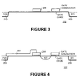
- a protective layer 401 (seen in Figure 4) is deposited, patterned, and etched such that the protective layer 401 covers the interface between the transfer gate and the photodiode region.
- the protective layer 401 is a nitride layer having a thickness of approximately 500 angstroms.
- other protective layers may also be used.
- One important consideration is that the interface between the transfer gate and the photodiode be protected from a subsequent re-oxidation step. While the protective layer 401 is shown extending to the field oxide 203, this is not absolutely necessary.
- Figure 4 is merely illustrative of a single embodiment of the present invention.
- a re-oxidation process is performed which will result in a thickening of the gate oxide near the floating diffusion 107 and transfer gate 206.
- the re-oxidation is performed using a rapid thermal oxidation (RTO) process.
- RTO rapid thermal oxidation
- This thickened gate oxide near the floating diffusion is beneficial as it reduces the leakage current through the channel-LDD junction. It prevents leakage of charge from the floating diffusion.
- near the photodiode interface with the transfer gate 206 there is no thickening of the gate oxide. This absence of a bird's beak at that location will enhance the electrical field. This increases the coupling between the N - region of the photodiode and the channel under the transfer gate. This facilitates the speedy and efficient transfer of the accumulated signal in the N - region of the photodiode to the floating node 501.
- the oxide above the floating diffusion 501 is thickened causing a bird's beak structure to be formed at the interface between the floating diffusion 501 and the transfer gate 206. Because of the protective layer 401, there is no formation of a bird's beak structure at the photodiode 503 interface to the transfer gate 206. Note also that in one embodiment, there is also a bird's beak structure at the interface between the reset gate of the reset transistor and the floating node 501.
- the protective layer 401 can be removed. Note that there is some ancillary oxide 505 formation on the side walls and the top of the transfer gate 206 in the reset gate. This ancillary oxide 505 may need to be removed to allow contact to the polysilicon gate material.
Landscapes
- Engineering & Computer Science (AREA)
- Multimedia (AREA)
- Signal Processing (AREA)
- Solid State Image Pick-Up Elements (AREA)
- Transforming Light Signals Into Electric Signals (AREA)
Abstract
Description
- The present invention relates to image sensors, and more particularly, to an image sensor that uses pixels having a transfer gate with an underlying asymmetric bird's beak smile.
- Image sensors have become ubiquitous. They are widely used in digital still cameras, cellular phones, security cameras, medical, automobile, and other applications. The technology used to manufacture image sensors, and in particular CMOS image sensors, has continued to advance at great pace. For example, the demands of higher resolution and lower power consumption have encouraged the further miniaturization and integration of the image sensor.
- Possibly as a result of the greater miniaturization and integration of the image sensor, various issues for both CMOS and CCD image sensors have arisen. For example, image lag and leakage current are important issues that need to be improved upon. As greater integration takes place, leakage current from a floating diffusion (also known as floating node) may become problematic. Specifically, leakage current through the channel-LDD (lightly doped drain) junction may occur. Additionally, image lag due to insufficient transfer of signal from the photodiode, through the channel of the transfer transistor, to the floating node is also an issue.
- These and other issues related to greater integration need to be addressed.
- Accordingly, in a first aspect, the present invention provides a method of forming an active pixel according to claim 1.
-
- Figure 1 is a cross-sectional view of a prior art four transistor (4T) pixel which shows in detail a photodiode formed in a substrate.
- Figures 2-5 are cross-sectional views of a process for forming a photodiode and pixel in accordance with the present invention.
- In the following description, numerous specific details are provided in order to give a thorough understanding of embodiments of the invention. One skilled in the relevant art will recognize, however, that the invention may be practiced without one or more of the specific details, or with other methods, components, materials, etc. In other instances, well known structures, materials, or operations are not shown or described in order to avoid obscuring aspects of the invention.
- References throughout the specification to "one embodiment" or "an embodiment" means that a particular feature, structure, or characteristic described in connection with the embodiment and included in at least one embodiment of the present invention. Thus, the appearances of the phrase "in one embodiment" or "in an embodiment" in various places throughout the specification are not necessarily all referring to the same embodiment. Furthermore, the particular features, structures, or characteristics may be combined in any suitable manner in one or more embodiments.
- Figure 1 shows a cross-sectional view of a prior art active pixel that uses four transistors. This is known in the art as a 4T active pixel. However, it can be appreciated that the photodiode design and process of the present invention can be used with any type of pixel design, including but not limited to 4T, 5T, 6T, and other designs. Further, the photodiode design of the present invention may also be used in connection with charge coupled device (CCD) imagers. The photodiode may also be a partially pinned photodiode.
- A
photodiode 101, outputs a signal that is used to modulate anamplification transistor 103. Theamplification transistor 103 is also referred to as a source follower transistor. In this embodiment, thephotodiode 101 can be either a pinned photodiode or a partially pinned photodiode. Thephotodiode 101 comprises a N- layer 115 that is a buried implant. Additionally, in one embodiment, a shallow P+ pinning layer 116 is formed at the surface of thesemiconductor substrate 102. - It should be noted that the
semiconductor substrate 102 is a p-type silicon substrate, but in other embodiments may be an n-type silicon substrate. Further, various structures are formed atop of and into thesilicon substrate 102. For example, thephotodiode 101 and thefloating node 107 are formed into thesilicon substrate 102. These structures are said to be formed below the surface of the silicon substrate by the use of dopants. Similarly, field oxides or shallow trench isolation structures are also formed at and below the top surface (or simply surface) of the silicon substrate. - In contrast, other structures, such as the
gate oxide 108, thetransfer gate 106, thetransfer transistor 105, and thereset transistor 113 are formed atop of thesilicon substrate 102 and are said to be at or above the top surface of the silicon substrate. - A
transfer transistor 105 is used to transfer the signal output by thephotodiode 101 to a floating node 107 (N+ doped), which is adjacent to the gate of thetransfer transistor 105. Thetransfer transistor 105 is controlled by atransfer gate 106. Thetransfer transistor 105 also has agate oxide 108 underneath thetransfer gate 106. - In operation, during an integration period (also referred to as an exposure or accumulation period), the
photodiode 101 stores charge that is held in the N- layer 115. After the integration period, thetransfer transistor 105 is turned on to transfer the charge held in the N-layer 115 of thephotodiode 101 to thefloating node 107. After the signal has been transferred to thefloating node 107, thetransfer transistor 105 is turned off again for the start of a subsequent integration period. - The signal on the
floating node 107 is then used to modulate theamplification transistor 103. Finally, anaddress transistor 109 is used as a means to address the pixel and to selectively read out the signal onto acolumn bitline 111. After readout through thecolumn bitline 111, areset transistor 113 resets thefloating node 107 to a reference voltage. In one embodiment, the reference voltage is Vdd. As seen in Figure 1, the N- layer 115 is linked to thetransfer transistor 105 by anarrow neck region 118. - The present invention will now be described in connection with Figures 2-5. Turning to Figure 2, a
semiconductor substrate 102 is shown. In one embodiment, thesemiconductor substrate 102 is a silicon substrate. Astandard isolation 203, such as a LOCOS field oxide, or a shallow trench isolation (STI) defines an active area within thesemiconductor substrate 102. In Figure 2, a field oxide is shown at one boundary and a STI is shown at another boundary of the pixel. This is meant to be illustrative of two different types of isolations, and in many embodiments, the boundary around a pixel will either be completely STI or completely LOCOS field oxide or completely another variety of isolation. In one embodiment, the field oxide or shallow trench isolation is lined with a P-type field implant. Theisolation 203 is used to electrically isolate an active area that will contain a pixel. - Still referring to Figure 2, a transistor gate stack is deposited and etched to form a stack of gate oxide/polysilicon (conductor). In one embodiment, the transistor gate stack is formed by the deposition or growth of a relatively thin gate oxide layer using conventional semiconductor processing methods, such as thermal growth or chemical vapor deposition. Next, a conductive layer, such as a polysilicon layer, is deposited over the gate oxide layer. The polysilicon layer (when patterned, etched, and possibly doped) will serve as the gate of the various transistors such as the
transfer transistor 105 or thereset transistor 113. - After deposition of these two layers, the stack is patterned and etched to leave the gate stack structures shown in Figure 2. These two structures will eventually form the
transfer gate 206 and the gate of thereset transistor 113. - The present invention utilizes the selective formation of "smiles" (also referred to as a bird's beak) during a re-oxidation of the
polysilicon transfer gate 206. As known by those skilled in the art, a bird's beak results from the lifting of a layer (such as polysilicon or nitride) due to an oxidation process. See www.sematech.org. This re-oxidation can occur and be implemented in several locations in the process flow. For example, turning to Figure 3, in one alternative embodiment, the gate stacks are formed by only etching the polysilicon layer and not the underlying gate oxide layer. In this embodiment, the gate oxide layer is left on the surface of thesemiconductor substrate 102. - Using either Figure 3 or Figure 2 as a starting point, a protective layer 401 (seen in Figure 4) is deposited, patterned, and etched such that the
protective layer 401 covers the interface between the transfer gate and the photodiode region. In one embodiment, theprotective layer 401 is a nitride layer having a thickness of approximately 500 angstroms. However, it can be appreciated that other protective layers may also be used. One important consideration is that the interface between the transfer gate and the photodiode be protected from a subsequent re-oxidation step. While theprotective layer 401 is shown extending to thefield oxide 203, this is not absolutely necessary. Thus, Figure 4 is merely illustrative of a single embodiment of the present invention. - Next, turning to Figure 5, a re-oxidation process is performed which will result in a thickening of the gate oxide near the floating
diffusion 107 andtransfer gate 206. In one embodiment, the re-oxidation is performed using a rapid thermal oxidation (RTO) process. This thickened gate oxide near the floating diffusion is beneficial as it reduces the leakage current through the channel-LDD junction. It prevents leakage of charge from the floating diffusion. However, near the photodiode interface with thetransfer gate 206, there is no thickening of the gate oxide. This absence of a bird's beak at that location will enhance the electrical field. This increases the coupling between the N- region of the photodiode and the channel under the transfer gate. This facilitates the speedy and efficient transfer of the accumulated signal in the N- region of the photodiode to the floating node 501. - Thus, turning to Figure 5, after the re-oxidation step, the oxide above the floating diffusion 501 is thickened causing a bird's beak structure to be formed at the interface between the floating diffusion 501 and the
transfer gate 206. Because of theprotective layer 401, there is no formation of a bird's beak structure at thephotodiode 503 interface to thetransfer gate 206. Note also that in one embodiment, there is also a bird's beak structure at the interface between the reset gate of the reset transistor and the floating node 501. - After the re-oxidation step, the
protective layer 401 can be removed. Note that there is someancillary oxide 505 formation on the side walls and the top of thetransfer gate 206 in the reset gate. Thisancillary oxide 505 may need to be removed to allow contact to the polysilicon gate material. - From the foregoing, it will be appreciated that specific embodiments of the invention have been described herein for purposes of illustration, but that various modifications may be made without deviating from the spirit and scope of the invention. Accordingly, the invention is not limited except as by the appended claims.
Claims (12)
- A method of forming an active pixel comprising:forming a photodiode in an active area of a semiconductor substrate;forming a transfer transistor between said photodiode and a floating node, said transfer transistor having a bird's beak structure formed at the interface of its transfer gate and said floating node; andforming a reset transistor operative for resetting said floating node to a voltage reference.
- The method of Claim 1 wherein said transfer transistor does not have a bird's beak structure at the interface of its transfer gate and said photodiode.
- The method of Claim 1 wherein said reset transistor has a bird's beak structure at both sides of its reset gate.
- The method of Claim 9 wherein said bird's beak structure is formed using a thermal re-oxidation.
- A method for forming a pixel comprising:forming an isolation in a semiconductor substrate to define an active area;forming a gate oxide over said active area;forming a polysilicon layer over said gate oxide;patterning said polysilicon layer to from a transfer gate and a reset gate;forming a photodiode in said semiconductor substrate and adjacent to said transfer gate;forming a floating node between said transfer gate and said reset gate;forming a protective layer over the interface of said transfer gate and said photodiode;performing a re-oxidation process to form a bird's beak structure at the interface of said transfer gate and said floating node.
- The method of Claim 5 further including removing said protective layer after said re-oxidation process.
- The method of Claim 6 wherein said protective layer is a nitride.
- The method of Claim 5 further wherein said re-oxidation process also forms a bird's beak structure at the interface of said reset gate and said floating node.
- A pixel comprising:a photodiode;a transfer transistor formed between said photodiode and a floating node and selectively operative to transfer a signal from said photodiode to said floating node, said transfer transistor having a bird's beak structure formed at the interface of its transfer gate and said floating node;a reset transistor for resetting said floating node to a voltage reference; andan amplification transistor controlled by said floating node.
- The pixel of Claim 9 wherein said transfer transistor does not have a bird's beak structure at the interface of its transfer gate and said photodiode.
- The pixel of Claim 9 wherein said reset transistor has a bird's beak structure at both sides of its reset gate.
- The pixel of Claim 9 wherein said bird's beak structure is formed using a thermal oxidation.
Applications Claiming Priority (1)
| Application Number | Priority Date | Filing Date | Title |
|---|---|---|---|
| US11/112,289 US20060240601A1 (en) | 2005-04-22 | 2005-04-22 | Selective smile formation under transfer gate in a CMOS image sensor pixel |
Publications (2)
| Publication Number | Publication Date |
|---|---|
| EP1715678A1 true EP1715678A1 (en) | 2006-10-25 |
| EP1715678B1 EP1715678B1 (en) | 2010-06-09 |
Family
ID=36755857
Family Applications (1)
| Application Number | Title | Priority Date | Filing Date |
|---|---|---|---|
| EP06251943A Expired - Lifetime EP1715678B1 (en) | 2005-04-22 | 2006-04-06 | Selective smile formation under transfer gate in a CMOS image sensor pixel |
Country Status (6)
| Country | Link |
|---|---|
| US (2) | US20060240601A1 (en) |
| EP (1) | EP1715678B1 (en) |
| CN (1) | CN100411142C (en) |
| AT (1) | ATE471035T1 (en) |
| DE (1) | DE602006014756D1 (en) |
| TW (1) | TW200638537A (en) |
Families Citing this family (8)
| Publication number | Priority date | Publication date | Assignee | Title |
|---|---|---|---|---|
| KR100810423B1 (en) * | 2006-12-27 | 2008-03-04 | 동부일렉트로닉스 주식회사 | Image sensor and manufacturing method of image sensor |
| US8319262B2 (en) * | 2009-07-31 | 2012-11-27 | Sri International | Substrate bias for CMOS imagers |
| CN101707202B (en) * | 2009-11-20 | 2012-01-11 | 苏州东微半导体有限公司 | Semiconductor photosensitization device, production method and application thereof |
| CN103779365B (en) | 2012-10-19 | 2016-06-22 | 比亚迪股份有限公司 | The imageing sensor of wide dynamic range pixel unit, its manufacture method and composition thereof |
| US9887234B2 (en) | 2014-01-24 | 2018-02-06 | Taiwan Semiconductor Manufacturing Company Limited | CMOS image sensor and method for forming the same |
| CN104010142B (en) * | 2014-06-12 | 2018-03-27 | 北京思比科微电子技术股份有限公司 | Active pixel and imaging sensor and its control sequential |
| CN104992954B (en) * | 2015-05-27 | 2018-08-28 | 上海华力微电子有限公司 | A method of reducing imaging sensor dark current |
| US10255968B2 (en) * | 2017-07-24 | 2019-04-09 | Omnivision Technologies, Inc. | DRAM core architecture with wide I/Os |
Citations (5)
| Publication number | Priority date | Publication date | Assignee | Title |
|---|---|---|---|---|
| WO2000021280A1 (en) * | 1998-10-07 | 2000-04-13 | California Institute Of Technology | Silicon-on-insulator (soi) active pixel sensors with the photosites implemented in the substrate |
| US6329233B1 (en) * | 2000-06-23 | 2001-12-11 | United Microelectronics Corp. | Method of manufacturing photodiode CMOS image sensor |
| US20020008767A1 (en) * | 2000-02-11 | 2002-01-24 | Do-Young Lee | Pixel layout for CMOS image sensor |
| US6351002B1 (en) * | 2000-07-03 | 2002-02-26 | United Microelectronics Corp. | Photodiode |
| US20040075110A1 (en) * | 2002-10-22 | 2004-04-22 | Taiwan Semiconductor Manufacturing Company | Asymmetrical reset transistor with double-diffused source for CMOS image sensor |
Family Cites Families (5)
| Publication number | Priority date | Publication date | Assignee | Title |
|---|---|---|---|---|
| US5371026A (en) * | 1992-11-30 | 1994-12-06 | Motorola Inc. | Method for fabricating paired MOS transistors having a current-gain differential |
| US5595922A (en) * | 1994-10-28 | 1997-01-21 | Texas Instruments | Process for thickening selective gate oxide regions |
| DE19812212A1 (en) * | 1998-03-19 | 1999-09-23 | Siemens Ag | MOS transistor in a one-transistor memory cell with a locally thickened gate oxide and manufacturing method |
| US6335254B1 (en) * | 2000-08-09 | 2002-01-01 | Micron Technology, Inc. | Methods of forming transistors |
| JP2003264277A (en) * | 2002-03-07 | 2003-09-19 | Fujitsu Ltd | CMOS image sensor and method of manufacturing the same |
-
2005
- 2005-04-22 US US11/112,289 patent/US20060240601A1/en not_active Abandoned
-
2006
- 2006-03-23 TW TW095110147A patent/TW200638537A/en unknown
- 2006-04-06 DE DE602006014756T patent/DE602006014756D1/en not_active Expired - Lifetime
- 2006-04-06 EP EP06251943A patent/EP1715678B1/en not_active Expired - Lifetime
- 2006-04-06 AT AT06251943T patent/ATE471035T1/en not_active IP Right Cessation
- 2006-04-24 CN CNB2006100792595A patent/CN100411142C/en not_active Expired - Lifetime
-
2007
- 2007-10-12 US US11/974,436 patent/US20080035940A1/en not_active Abandoned
Patent Citations (6)
| Publication number | Priority date | Publication date | Assignee | Title |
|---|---|---|---|---|
| WO2000021280A1 (en) * | 1998-10-07 | 2000-04-13 | California Institute Of Technology | Silicon-on-insulator (soi) active pixel sensors with the photosites implemented in the substrate |
| US20020008767A1 (en) * | 2000-02-11 | 2002-01-24 | Do-Young Lee | Pixel layout for CMOS image sensor |
| US6329233B1 (en) * | 2000-06-23 | 2001-12-11 | United Microelectronics Corp. | Method of manufacturing photodiode CMOS image sensor |
| US20010055849A1 (en) * | 2000-06-23 | 2001-12-27 | Jui-Hsiang Pan | Method of manufacturing photodiode CMOS image sensor |
| US6351002B1 (en) * | 2000-07-03 | 2002-02-26 | United Microelectronics Corp. | Photodiode |
| US20040075110A1 (en) * | 2002-10-22 | 2004-04-22 | Taiwan Semiconductor Manufacturing Company | Asymmetrical reset transistor with double-diffused source for CMOS image sensor |
Also Published As
| Publication number | Publication date |
|---|---|
| US20080035940A1 (en) | 2008-02-14 |
| EP1715678B1 (en) | 2010-06-09 |
| CN100411142C (en) | 2008-08-13 |
| US20060240601A1 (en) | 2006-10-26 |
| CN1851902A (en) | 2006-10-25 |
| DE602006014756D1 (en) | 2010-07-22 |
| TW200638537A (en) | 2006-11-01 |
| ATE471035T1 (en) | 2010-06-15 |
Similar Documents
| Publication | Publication Date | Title |
|---|---|---|
| CN1979883B (en) | Solid-state imaging device and image apparatus | |
| US7524695B2 (en) | Image sensor and pixel having an optimized floating diffusion | |
| US8541825B2 (en) | Image sensor with improved charge transfer efficiency and method for fabricating the same | |
| US20080035940A1 (en) | Selective smile formation under transfer gate in a CMOS image sensor pixel | |
| JP2006191095A (en) | CMOS image sensor and manufacturing method thereof | |
| US7344910B2 (en) | Self-aligned photodiode for CMOS image sensor and method of making | |
| JP4384113B2 (en) | CMOS image sensor | |
| US20090215221A1 (en) | Image sensor and method for manufacturing the same | |
| US7361527B2 (en) | Image sensor with improved charge transfer efficiency and method for fabricating the same | |
| CN105575986A (en) | Solid-state imaging device and method of manufacturing solid-state imaging device | |
| US8076207B2 (en) | Gate structure and method of making the same | |
| US20070012962A1 (en) | Method for making image sensor with reduced etching damage | |
| US8129765B2 (en) | CMOS image sensor with photo-detector protecting layers | |
| US20160148961A1 (en) | Active pixel sensor having a raised source/drain | |
| CN100483683C (en) | CMOS image sensor and manufacturing method thereof | |
| JP2006024934A (en) | Manufacturing method of CMOS image sensor | |
| EP1746656A2 (en) | Pixel sensor with raised silicon photodiode | |
| KR100477791B1 (en) | Method for manufacturing a cmos image sensor | |
| US7659133B2 (en) | Method for manufacturing CMOS image sensor | |
| KR20100045110A (en) | Method for fabricating of cmos image sensor | |
| KR100937674B1 (en) | Manufacturing Method of CMOS Image Sensor | |
| KR20020014315A (en) | Image sensor formation method capable of preventing cross talk between pixels and reduction of active area | |
| KR100788379B1 (en) | Manufacturing Method of Image Sensor | |
| KR100749254B1 (en) | Manufacturing method of image sensor to improve charge transport efficiency | |
| JP2005251945A (en) | Solid-state imaging device, manufacturing method thereof, and camera using solid-state imaging device |
Legal Events
| Date | Code | Title | Description |
|---|---|---|---|
| PUAI | Public reference made under article 153(3) epc to a published international application that has entered the european phase |
Free format text: ORIGINAL CODE: 0009012 |
|
| 17P | Request for examination filed |
Effective date: 20060425 |
|
| AK | Designated contracting states |
Kind code of ref document: A1 Designated state(s): AT BE BG CH CY CZ DE DK EE ES FI FR GB GR HU IE IS IT LI LT LU LV MC NL PL PT RO SE SI SK TR |
|
| AX | Request for extension of the european patent |
Extension state: AL BA HR MK YU |
|
| 17Q | First examination report despatched |
Effective date: 20070516 |
|
| AKX | Designation fees paid |
Designated state(s): AT BE BG CH CY CZ DE DK EE ES FI FR GB GR HU IE IS IT LI LT LU LV MC NL PL PT RO SE SI SK TR |
|
| GRAP | Despatch of communication of intention to grant a patent |
Free format text: ORIGINAL CODE: EPIDOSNIGR1 |
|
| GRAS | Grant fee paid |
Free format text: ORIGINAL CODE: EPIDOSNIGR3 |
|
| GRAA | (expected) grant |
Free format text: ORIGINAL CODE: 0009210 |
|
| AK | Designated contracting states |
Kind code of ref document: B1 Designated state(s): AT BE BG CH CY CZ DE DK EE ES FI FR GB GR HU IE IS IT LI LT LU LV MC NL PL PT RO SE SI SK TR |
|
| REG | Reference to a national code |
Ref country code: CH Ref legal event code: EP |
|
| REG | Reference to a national code |
Ref country code: IE Ref legal event code: FG4D |
|
| REF | Corresponds to: |
Ref document number: 602006014756 Country of ref document: DE Date of ref document: 20100722 Kind code of ref document: P |
|
| REG | Reference to a national code |
Ref country code: NL Ref legal event code: VDEP Effective date: 20100609 |
|
| PG25 | Lapsed in a contracting state [announced via postgrant information from national office to epo] |
Ref country code: SE Free format text: LAPSE BECAUSE OF FAILURE TO SUBMIT A TRANSLATION OF THE DESCRIPTION OR TO PAY THE FEE WITHIN THE PRESCRIBED TIME-LIMIT Effective date: 20100609 Ref country code: LT Free format text: LAPSE BECAUSE OF FAILURE TO SUBMIT A TRANSLATION OF THE DESCRIPTION OR TO PAY THE FEE WITHIN THE PRESCRIBED TIME-LIMIT Effective date: 20100609 |
|
| LTIE | Lt: invalidation of european patent or patent extension |
Effective date: 20100609 |
|
| PG25 | Lapsed in a contracting state [announced via postgrant information from national office to epo] |
Ref country code: SI Free format text: LAPSE BECAUSE OF FAILURE TO SUBMIT A TRANSLATION OF THE DESCRIPTION OR TO PAY THE FEE WITHIN THE PRESCRIBED TIME-LIMIT Effective date: 20100609 Ref country code: FI Free format text: LAPSE BECAUSE OF FAILURE TO SUBMIT A TRANSLATION OF THE DESCRIPTION OR TO PAY THE FEE WITHIN THE PRESCRIBED TIME-LIMIT Effective date: 20100609 Ref country code: AT Free format text: LAPSE BECAUSE OF FAILURE TO SUBMIT A TRANSLATION OF THE DESCRIPTION OR TO PAY THE FEE WITHIN THE PRESCRIBED TIME-LIMIT Effective date: 20100609 Ref country code: LV Free format text: LAPSE BECAUSE OF FAILURE TO SUBMIT A TRANSLATION OF THE DESCRIPTION OR TO PAY THE FEE WITHIN THE PRESCRIBED TIME-LIMIT Effective date: 20100609 |
|
| PG25 | Lapsed in a contracting state [announced via postgrant information from national office to epo] |
Ref country code: GR Free format text: LAPSE BECAUSE OF FAILURE TO SUBMIT A TRANSLATION OF THE DESCRIPTION OR TO PAY THE FEE WITHIN THE PRESCRIBED TIME-LIMIT Effective date: 20100910 Ref country code: CY Free format text: LAPSE BECAUSE OF FAILURE TO SUBMIT A TRANSLATION OF THE DESCRIPTION OR TO PAY THE FEE WITHIN THE PRESCRIBED TIME-LIMIT Effective date: 20100609 Ref country code: PL Free format text: LAPSE BECAUSE OF FAILURE TO SUBMIT A TRANSLATION OF THE DESCRIPTION OR TO PAY THE FEE WITHIN THE PRESCRIBED TIME-LIMIT Effective date: 20100609 |
|
| PG25 | Lapsed in a contracting state [announced via postgrant information from national office to epo] |
Ref country code: EE Free format text: LAPSE BECAUSE OF FAILURE TO SUBMIT A TRANSLATION OF THE DESCRIPTION OR TO PAY THE FEE WITHIN THE PRESCRIBED TIME-LIMIT Effective date: 20100609 Ref country code: NL Free format text: LAPSE BECAUSE OF FAILURE TO SUBMIT A TRANSLATION OF THE DESCRIPTION OR TO PAY THE FEE WITHIN THE PRESCRIBED TIME-LIMIT Effective date: 20100609 |
|
| PG25 | Lapsed in a contracting state [announced via postgrant information from national office to epo] |
Ref country code: RO Free format text: LAPSE BECAUSE OF FAILURE TO SUBMIT A TRANSLATION OF THE DESCRIPTION OR TO PAY THE FEE WITHIN THE PRESCRIBED TIME-LIMIT Effective date: 20100609 Ref country code: IS Free format text: LAPSE BECAUSE OF FAILURE TO SUBMIT A TRANSLATION OF THE DESCRIPTION OR TO PAY THE FEE WITHIN THE PRESCRIBED TIME-LIMIT Effective date: 20101009 Ref country code: BE Free format text: LAPSE BECAUSE OF FAILURE TO SUBMIT A TRANSLATION OF THE DESCRIPTION OR TO PAY THE FEE WITHIN THE PRESCRIBED TIME-LIMIT Effective date: 20100609 Ref country code: CZ Free format text: LAPSE BECAUSE OF FAILURE TO SUBMIT A TRANSLATION OF THE DESCRIPTION OR TO PAY THE FEE WITHIN THE PRESCRIBED TIME-LIMIT Effective date: 20100609 Ref country code: SK Free format text: LAPSE BECAUSE OF FAILURE TO SUBMIT A TRANSLATION OF THE DESCRIPTION OR TO PAY THE FEE WITHIN THE PRESCRIBED TIME-LIMIT Effective date: 20100609 Ref country code: PT Free format text: LAPSE BECAUSE OF FAILURE TO SUBMIT A TRANSLATION OF THE DESCRIPTION OR TO PAY THE FEE WITHIN THE PRESCRIBED TIME-LIMIT Effective date: 20101011 |
|
| PG25 | Lapsed in a contracting state [announced via postgrant information from national office to epo] |
Ref country code: IT Free format text: LAPSE BECAUSE OF FAILURE TO SUBMIT A TRANSLATION OF THE DESCRIPTION OR TO PAY THE FEE WITHIN THE PRESCRIBED TIME-LIMIT Effective date: 20100609 |
|
| PLBE | No opposition filed within time limit |
Free format text: ORIGINAL CODE: 0009261 |
|
| STAA | Information on the status of an ep patent application or granted ep patent |
Free format text: STATUS: NO OPPOSITION FILED WITHIN TIME LIMIT |
|
| PG25 | Lapsed in a contracting state [announced via postgrant information from national office to epo] |
Ref country code: DK Free format text: LAPSE BECAUSE OF FAILURE TO SUBMIT A TRANSLATION OF THE DESCRIPTION OR TO PAY THE FEE WITHIN THE PRESCRIBED TIME-LIMIT Effective date: 20100609 |
|
| 26N | No opposition filed |
Effective date: 20110310 |
|
| REG | Reference to a national code |
Ref country code: DE Ref legal event code: R097 Ref document number: 602006014756 Country of ref document: DE Effective date: 20110309 |
|
| PG25 | Lapsed in a contracting state [announced via postgrant information from national office to epo] |
Ref country code: MC Free format text: LAPSE BECAUSE OF NON-PAYMENT OF DUE FEES Effective date: 20110430 |
|
| REG | Reference to a national code |
Ref country code: CH Ref legal event code: PL |
|
| PG25 | Lapsed in a contracting state [announced via postgrant information from national office to epo] |
Ref country code: CH Free format text: LAPSE BECAUSE OF NON-PAYMENT OF DUE FEES Effective date: 20110430 Ref country code: LI Free format text: LAPSE BECAUSE OF NON-PAYMENT OF DUE FEES Effective date: 20110430 |
|
| REG | Reference to a national code |
Ref country code: IE Ref legal event code: MM4A |
|
| PG25 | Lapsed in a contracting state [announced via postgrant information from national office to epo] |
Ref country code: IE Free format text: LAPSE BECAUSE OF NON-PAYMENT OF DUE FEES Effective date: 20110406 |
|
| PG25 | Lapsed in a contracting state [announced via postgrant information from national office to epo] |
Ref country code: LU Free format text: LAPSE BECAUSE OF NON-PAYMENT OF DUE FEES Effective date: 20110406 |
|
| PG25 | Lapsed in a contracting state [announced via postgrant information from national office to epo] |
Ref country code: BG Free format text: LAPSE BECAUSE OF FAILURE TO SUBMIT A TRANSLATION OF THE DESCRIPTION OR TO PAY THE FEE WITHIN THE PRESCRIBED TIME-LIMIT Effective date: 20100909 Ref country code: TR Free format text: LAPSE BECAUSE OF FAILURE TO SUBMIT A TRANSLATION OF THE DESCRIPTION OR TO PAY THE FEE WITHIN THE PRESCRIBED TIME-LIMIT Effective date: 20100609 |
|
| PG25 | Lapsed in a contracting state [announced via postgrant information from national office to epo] |
Ref country code: ES Free format text: LAPSE BECAUSE OF FAILURE TO SUBMIT A TRANSLATION OF THE DESCRIPTION OR TO PAY THE FEE WITHIN THE PRESCRIBED TIME-LIMIT Effective date: 20100920 Ref country code: HU Free format text: LAPSE BECAUSE OF FAILURE TO SUBMIT A TRANSLATION OF THE DESCRIPTION OR TO PAY THE FEE WITHIN THE PRESCRIBED TIME-LIMIT Effective date: 20100609 |
|
| REG | Reference to a national code |
Ref country code: FR Ref legal event code: PLFP Year of fee payment: 11 |
|
| REG | Reference to a national code |
Ref country code: FR Ref legal event code: PLFP Year of fee payment: 12 |
|
| REG | Reference to a national code |
Ref country code: FR Ref legal event code: PLFP Year of fee payment: 13 |
|
| REG | Reference to a national code |
Ref country code: DE Ref legal event code: R079 Ref document number: 602006014756 Country of ref document: DE Free format text: PREVIOUS MAIN CLASS: H04N0005335000 Ipc: H04N0025000000 |
|
| PGFP | Annual fee paid to national office [announced via postgrant information from national office to epo] |
Ref country code: FR Payment date: 20250319 Year of fee payment: 20 |
|
| PGFP | Annual fee paid to national office [announced via postgrant information from national office to epo] |
Ref country code: GB Payment date: 20250313 Year of fee payment: 20 |
|
| PGFP | Annual fee paid to national office [announced via postgrant information from national office to epo] |
Ref country code: DE Payment date: 20250317 Year of fee payment: 20 |
|
| REG | Reference to a national code |
Ref country code: DE Ref legal event code: R071 Ref document number: 602006014756 Country of ref document: DE |
|
| REG | Reference to a national code |
Ref country code: GB Ref legal event code: PE20 Expiry date: 20260405 |