EP1715527A2 - Electrostatic discharge protection device - Google Patents
Electrostatic discharge protection device Download PDFInfo
- Publication number
- EP1715527A2 EP1715527A2 EP06075812A EP06075812A EP1715527A2 EP 1715527 A2 EP1715527 A2 EP 1715527A2 EP 06075812 A EP06075812 A EP 06075812A EP 06075812 A EP06075812 A EP 06075812A EP 1715527 A2 EP1715527 A2 EP 1715527A2
- Authority
- EP
- European Patent Office
- Prior art keywords
- type
- type well
- region
- well
- substrate
- Prior art date
- Legal status (The legal status is an assumption and is not a legal conclusion. Google has not performed a legal analysis and makes no representation as to the accuracy of the status listed.)
- Withdrawn
Links
- 239000000758 substrate Substances 0.000 claims abstract description 32
- 238000009792 diffusion process Methods 0.000 description 29
- 230000015556 catabolic process Effects 0.000 description 27
- 239000004065 semiconductor Substances 0.000 description 11
- 239000002184 metal Substances 0.000 description 8
- 238000013461 design Methods 0.000 description 6
- 239000000463 material Substances 0.000 description 4
- 238000013459 approach Methods 0.000 description 2
- 239000002800 charge carrier Substances 0.000 description 2
- 239000007943 implant Substances 0.000 description 2
- 238000002513 implantation Methods 0.000 description 2
- 238000000034 method Methods 0.000 description 2
- 239000007787 solid Substances 0.000 description 2
- VMXJCRHCUWKQCB-UHFFFAOYSA-N NPNP Chemical compound NPNP VMXJCRHCUWKQCB-UHFFFAOYSA-N 0.000 description 1
- 229910044991 metal oxide Inorganic materials 0.000 description 1
- 150000004706 metal oxides Chemical class 0.000 description 1
- 238000012986 modification Methods 0.000 description 1
- 230000004048 modification Effects 0.000 description 1
- 238000005457 optimization Methods 0.000 description 1
- 238000012545 processing Methods 0.000 description 1
- 229910052710 silicon Inorganic materials 0.000 description 1
- 239000010703 silicon Substances 0.000 description 1
- 230000001052 transient effect Effects 0.000 description 1
Images

Classifications
-
- H—ELECTRICITY
- H10—SEMICONDUCTOR DEVICES; ELECTRIC SOLID-STATE DEVICES NOT OTHERWISE PROVIDED FOR
- H10D—INORGANIC ELECTRIC SEMICONDUCTOR DEVICES
- H10D8/00—Diodes
- H10D8/80—PNPN diodes, e.g. Shockley diodes or break-over diodes
-
- H—ELECTRICITY
- H10—SEMICONDUCTOR DEVICES; ELECTRIC SOLID-STATE DEVICES NOT OTHERWISE PROVIDED FOR
- H10D—INORGANIC ELECTRIC SEMICONDUCTOR DEVICES
- H10D62/00—Semiconductor bodies, or regions thereof, of devices having potential barriers
- H10D62/10—Shapes, relative sizes or dispositions of the regions of the semiconductor bodies; Shapes of the semiconductor bodies
- H10D62/102—Constructional design considerations for preventing surface leakage or controlling electric field concentration
- H10D62/103—Constructional design considerations for preventing surface leakage or controlling electric field concentration for increasing or controlling the breakdown voltage of reverse-biased devices
- H10D62/105—Constructional design considerations for preventing surface leakage or controlling electric field concentration for increasing or controlling the breakdown voltage of reverse-biased devices by having particular doping profiles, shapes or arrangements of PN junctions; by having supplementary regions, e.g. junction termination extension [JTE]
- H10D62/108—Constructional design considerations for preventing surface leakage or controlling electric field concentration for increasing or controlling the breakdown voltage of reverse-biased devices by having particular doping profiles, shapes or arrangements of PN junctions; by having supplementary regions, e.g. junction termination extension [JTE] having localised breakdown regions, e.g. built-in avalanching regions
-
- H—ELECTRICITY
- H10—SEMICONDUCTOR DEVICES; ELECTRIC SOLID-STATE DEVICES NOT OTHERWISE PROVIDED FOR
- H10D—INORGANIC ELECTRIC SEMICONDUCTOR DEVICES
- H10D8/00—Diodes
- H10D8/411—PN diodes having planar bodies
-
- H—ELECTRICITY
- H10—SEMICONDUCTOR DEVICES; ELECTRIC SOLID-STATE DEVICES NOT OTHERWISE PROVIDED FOR
- H10D—INORGANIC ELECTRIC SEMICONDUCTOR DEVICES
- H10D89/00—Aspects of integrated devices not covered by groups H10D84/00 - H10D88/00
- H10D89/60—Integrated devices comprising arrangements for electrical or thermal protection, e.g. protection circuits against electrostatic discharge [ESD]
- H10D89/601—Integrated devices comprising arrangements for electrical or thermal protection, e.g. protection circuits against electrostatic discharge [ESD] for devices having insulated gate electrodes, e.g. for IGFETs or IGBTs
- H10D89/711—Integrated devices comprising arrangements for electrical or thermal protection, e.g. protection circuits against electrostatic discharge [ESD] for devices having insulated gate electrodes, e.g. for IGFETs or IGBTs using bipolar transistors as protective elements
- H10D89/713—Integrated devices comprising arrangements for electrical or thermal protection, e.g. protection circuits against electrostatic discharge [ESD] for devices having insulated gate electrodes, e.g. for IGFETs or IGBTs using bipolar transistors as protective elements including a PNP transistor and a NPN transistor, wherein each of said transistors has its base region coupled to the collector region of the other transistor, e.g. silicon controlled rectifier [SCR] devices
Definitions
- the present invention is generally directed to a protection device and, more specifically, an electrostatic discharge protection device.
- the conventional thyristor is a four-layer or four-diffusion semiconductor device, with alternating N-type and P-type layers or diffusions, e.g., NPNP or PNPN.
- the main terminals (i.e., anode and cathode) of a thyristor are across all four layers or diffusions and a control terminal (i.e., gate) is attached to one of the middle layers or diffusions.
- the operation of a thyristor can generally be understood in terms of a pair of coupled transistors (i.e., an NPN transistor and a PNP transistor), arranged to cause a self-latching action.
- a conventional thyristor is that, like a diode, it only conducts in one direction.
- Another drawback associated with a conventional thyristor is that it is not a fully controllable switch, in the sense that the triggering current direction needs to be reversed to switch the thyristor off.
- Yet another shortcoming of a conventional thyristor is that it is not readily integrated with a semiconductor device that is to be protected.
- What is needed is a protection device that can be readily integrated with a semiconductor device that is to be protected from electrostatic discharge.
- an electrostatic discharge (ESD) protection device includes a first-type substrate, a second-type well formed in the substrate and a first first-type well formed in the substrate.
- the second-type well includes a second-type+ region formed between a first and second first-type+ region.
- the first first-type well is formed in the substrate adjacent the second-type well.
- the first first-type well includes first and second first-type regions with a first-type+ region and a second-type+ region formed between the first and second first-type regions.
- the second+ region of the first first-type well is formed between the first-type+ region of the first first-type well and the second-type well.
- the second-type well and the first first-type well are one of abutted, overlapped and spaced apart from one another.
- a second first-type well is also formed in the substrate adjacent the second-type well opposite the first first-type well.
- the first-type well includes first and second first-type regions with a first-type+ region and a second-type+ region formed between the first and second first-type regions.
- the second-type+ region of the second first-type well is formed between the first-type+ region of the second first-type well and the second-type well.
- the device is a Shockley diode.
- the first-type is a P-type and the second-type is an N-type.
- an electrostatic discharge (ESD) protection device in operation, provides the functionality of a Shockley diode.
- One design layout for the protection device uses the proximity of twin P-type wells to an N-type well, both formed in a P-type substrate, to set a first breakdown voltage.
- the current density at which the device snaps back is set by a width of counter-doped shallow N+ and P+ diffusions, which are located inside the N-type well and P-type wells, and by a sheet resistance of the N-type well and the P-type wells.
- the breakdown voltage BV ceo of an internal NPN transistor is set by the spacing of an N+ shallow diffusion, which is nested inside the P-type well, to its adjacent N-type well.
- a protection device may be designed to be integrated into a complimentary metal-oxide semiconductor (CMOS) process and, in this manner, readily protect various device pins at voltages up to about 60 Volts or higher.
- CMOS complimentary metal-oxide semiconductor
- the layout of the device may be designed to be less sensitive by arranging P-type wells on opposite sides of a central N-type well. When self-aligned twin wells are utilized, the device does not need to be laid out as a symmetric structure.
- first-type and second-type refer to opposite types.
- an N-type semiconductor material is a semiconductor material in which the predominant charge carriers are electrons and a P-type semiconductor material is a semiconductor material in which the predominant charge carriers are holes (positive charges).
- a + sign indicates very heavy doping approaching the solid solubility limit.
- an N-type+ region is an N-type region where the doping approaches the solid solubility region.
- the device 100 may be fabricated utilizing a P-type substrate 102 that includes a centrally located N-type well 106 and twin P-type wells 104 and 108 located on opposite sides of the N-type well 106.
- the P-type substrate 102 may have a (100) Miller indice.
- the N-type well 106 and the P-type wells 104 and 108 are masked and implanted into the P-type substrate 102.
- the wells 104, 106 and 108 are then driven into (e.g., to a depth of 4 ⁇ m) the P-type substrate 102. As is shown in Fig.
- a P-type well is located on opposite sides of the N-type well. It should be appreciated that, according to the present invention, the N-type well and the P-type wells can be abutted, overlapped or spaced away from one another to achieve desired characteristics for the device 100.
- the protection device 100 of Fig. 1 is depicted after a number of additional steps. That is, after implantation of the P-type wells (anode) 104 and 108 and the N-type well (cathode) 106 into the P-type substrate 102, the P-type substrate 102 is masked and shallow P-type regions (PFLD) 110 are implanted into the P-type wells 104 and 108. A field oxide 150 is then grown leaving active area regions associated with the P-type wells 104 and 108 and the N-type well 106.
- PFLD P-type regions
- Shallow N+ and P+ regions are then implanted into (e.g., to a depth of 0.3 ⁇ m) the P-type wells 104 and 108 and the N-type well 106.
- P+ diffusions 112 and N+ diffusions 114 are implanted into the P-type wells 104 and 108 and P+ diffusions 122 are implanted into the N-type well 106 on either side of an implanted N+ diffusion 124.
- the shallow diffusions are driven into the silicon of the P-type wells 104 and 108 and the N-type well 106.
- a first dielectric layer is added to cover the diffusions.
- contact holes are etched through the first dielectric layer.
- metal runners 140, 142 and 144 are deposited and defined. As is shown in Fig. 2, the metal runner 140 contacts the P+ diffusion 112 and the N+ diffusion 114 located in the P-type well 104 and the metal runner 144 contacts the P+ diffusion 112 and the N+ diffusion 114 located in the P-type well 108.
- the metal runners 140 and 142 are interconnected.
- An oxide layer 134 electrically isolates the runner 140 from an adjacent runner.
- the metal runner 142 contacts the P+ regions 122 and the N+ region 124 located in the N-type well 106.
- oxide layers 130 and 132 isolate the runner 142 from adjacent runners 140 and 144. It should be appreciated that the device 100 shown in Fig. 2 is a relatively non-complex device and that more dielectric and metal layers may be added to the device 100 to achieve a desired connectivity.
- the metal runner 142 is electrically coupled to a cathode of the device 100 and is also connected to an output circuit pad, along with other circuit elements that are to be protected from ESD stress.
- the cathode remains off, due to the high breakdown voltage of the N-type well 106 to P-type wells 104 and 108 and N-type well 106 to P-type substrate 102.
- the voltage on the cathode exceeds the breakdown voltage of the N-type well 106 to P-type wells 104 and 108.
- a graph 200 includes a curve 210 that plots the voltage of the device 100 with respect to the logarithmic current through the device (illustrated diode) 100. As is shown, a first breakdown voltage is reached at a first breakdown 212 on curve 210.
- the spacing 'C', which is the width of the P-type well 104 enclosure of the N+ diffusion 114, and the total doping concentration of the P-type well 104 under the N+ diffusion 114 is required to be sufficient to prevent N+ punch-through and early breakdown.
- the spacing 'D' which is the width of the N-type well 106 enclosure of the P+ diffusion 122, and the total doping concentration of the N-type well 106 under the P+ diffusion 112 is required to be sufficient to prevent P+ punch-through and early breakdown. It is also desirable that the metal from the anode and cathode of the device 100 do not overlap the point at which the N-type well 106 and P-type well 104 meet in order to have no influence on the level of the first breakdown voltage.
- a width 'E' of the N+ diffusion 114 multiplied by the sheet resistance of the P-type well 104, under the N+ diffusion 114, sets the critical current density required to trigger a second breakdown 214, as shown by curve 210A.
- Increasing the width the N+ diffusion 114 and the sheet resistance of the P-type well 104 causes the breakdown of the device 100 to occur at lower voltage and current levels, as the base-emitter voltage required to turn on the illustrated NPN transistor develops at a lower overall current density.
- delta V 224 may become large enough to cause the breakdown voltage of the protection device 100 to exceed the breakdown voltage of the protected device.
- the second breakdown 214 occurs at a second breakdown voltage that is greater in magnitude than the first breakdown voltage.
- a width 'F' of the P+ diffusion 122 multiplied by the sheet resistance of the N-type well 106, under the P+ diffusion 122, sets the critical current density required to trigger a third breakdown 216, as shown on curve 210B.
- Increasing the width of the P+ diffusion 122 and the sheet resistance of the N-type well 106 causes the third breakdown 216 of the device 100 to occur at a lower voltage level, as the base-emitter voltage required to turn on the illustrated PNP transistor develops at a lower overall current density.
- the third breakdown 216 it is generally desirable for the third breakdown 216 to occur at a lower voltage level as the extra voltage (delta V 226) added to the second breakdown voltage forces more power through the protected device, reducing the ESD ruggedness of the protected device.
- the peak ESD protection power that can be achieved is directly related to the design of the parameter 'F' and the sheet resistance of the N-type well 106.
- the device 100 exhibits a relatively low on-resistance.
- An exemplary protection device may be constructed with the parameters A-F having the following values: A of about 0 ⁇ m; B of about 0.6 ⁇ m; C of about 4 ⁇ m; D of about 4 ⁇ m; E of about 8 ⁇ m; and F of about 8 ⁇ m.
- a protection device has been described herein that can be readily integrated with a semiconductor device that is to be protected from electrostatic discharge. This is particularly advantageous in an automotive environment due to increased usage of electronic components in motor vehicles.
Landscapes
- Semiconductor Integrated Circuits (AREA)
- Metal-Oxide And Bipolar Metal-Oxide Semiconductor Integrated Circuits (AREA)
Abstract
Description
- The present invention is generally directed to a protection device and, more specifically, an electrostatic discharge protection device.
- Traditionally, a number of devices have been utilized to protect semiconductor devices from high voltages, such as those that occur during electrostatic discharge (ESD). For example, conventional thyristors have been utilized to protect semiconductor devices from high voltages that result from ESD. In general, the conventional thyristor is a four-layer or four-diffusion semiconductor device, with alternating N-type and P-type layers or diffusions, e.g., NPNP or PNPN. The main terminals (i.e., anode and cathode) of a thyristor are across all four layers or diffusions and a control terminal (i.e., gate) is attached to one of the middle layers or diffusions. The operation of a thyristor can generally be understood in terms of a pair of coupled transistors (i.e., an NPN transistor and a PNP transistor), arranged to cause a self-latching action.
- One shortcoming of a conventional thyristor is that, like a diode, it only conducts in one direction. Another drawback associated with a conventional thyristor is that it is not a fully controllable switch, in the sense that the triggering current direction needs to be reversed to switch the thyristor off. Yet another shortcoming of a conventional thyristor is that it is not readily integrated with a semiconductor device that is to be protected.
- What is needed is a protection device that can be readily integrated with a semiconductor device that is to be protected from electrostatic discharge.
- According to an embodiment of the present invention, an electrostatic discharge (ESD) protection device includes a first-type substrate, a second-type well formed in the substrate and a first first-type well formed in the substrate. The second-type well includes a second-type+ region formed between a first and second first-type+ region. The first first-type well is formed in the substrate adjacent the second-type well. The first first-type well includes first and second first-type regions with a first-type+ region and a second-type+ region formed between the first and second first-type regions. The second+ region of the first first-type well is formed between the first-type+ region of the first first-type well and the second-type well.
- According to another aspect, the second-type well and the first first-type well are one of abutted, overlapped and spaced apart from one another. According to another embodiment, a second first-type well is also formed in the substrate adjacent the second-type well opposite the first first-type well. The first-type well includes first and second first-type regions with a first-type+ region and a second-type+ region formed between the first and second first-type regions. The second-type+ region of the second first-type well is formed between the first-type+ region of the second first-type well and the second-type well. According to another aspect, the device is a Shockley diode. According to yet another aspect, the first-type is a P-type and the second-type is an N-type.
- These and other features, advantages and objects of the present invention will be further understood and appreciated by those skilled in the art by reference to the following specification, claims and appended drawings.
- The present invention will now be described, by way of example, with reference to the accompanying drawings, in which:
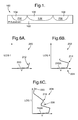
- Fig. 1 is a cross-sectional view of a relevant portion of a protection device, constructed according to one embodiment of the present invention, that includes a P-type substrate with an N-type well positioned between a pair of P-type wells;
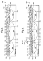
- Fig. 2 is a cross-sectional view of the protection device of Fig. 1 after additional processing;
- Fig. 3 is a cross-sectional view of the protection device of Fig. 2 with various design parameters illustrated;
- Fig. 4 depicts the protection device of Fig. 2 with an additional design parameter illustrated;
- Fig. 5 depicts the protection device of Fig. 2 with another additional design parameter illustrated;
- Fig. 6A is a graph that includes a curve that plots the voltage-current relationship of the device of Fig. 2 for a first breakdown point;
- Fig. 6B depicts a graph that includes a curve that plots the voltage-current relationship of the device of Fig. 2 for a first and second breakdown point; and
- Fig. 6C depicts a graph that includes a curve that plots the voltage-current relationship of the device of Fig. 2 for a first, second and third breakdown point.
- According to the present invention, an electrostatic discharge (ESD) protection device, in operation, provides the functionality of a Shockley diode. One design layout for the protection device uses the proximity of twin P-type wells to an N-type well, both formed in a P-type substrate, to set a first breakdown voltage. The current density at which the device snaps back is set by a width of counter-doped shallow N+ and P+ diffusions, which are located inside the N-type well and P-type wells, and by a sheet resistance of the N-type well and the P-type wells. The breakdown voltage BVceo of an internal NPN transistor is set by the spacing of an N+ shallow diffusion, which is nested inside the P-type well, to its adjacent N-type well.
- Through optimization of the layout and sheet resistance variables, a protection device may be designed to be integrated into a complimentary metal-oxide semiconductor (CMOS) process and, in this manner, readily protect various device pins at voltages up to about 60 Volts or higher. In general, the layout of the device may be designed to be less sensitive by arranging P-type wells on opposite sides of a central N-type well. When self-aligned twin wells are utilized, the device does not need to be laid out as a symmetric structure.
- While the discussion herein is directed to a device having an N-type well and P-type wells formed in a P-type substrate, it should be appreciated that the types of the wells and substrate may be reversed. In this case, the other regions, discussed below, would also be reversed in type. As used herein, the terms "first-type" and "second-type" refer to opposite types. For example, if the first-type is P-type, then the second-type is N-type. As is well know to those of ordinary skill in the art, an N-type semiconductor material is a semiconductor material in which the predominant charge carriers are electrons and a P-type semiconductor material is a semiconductor material in which the predominant charge carriers are holes (positive charges). As used herein a + sign indicates very heavy doping approaching the solid solubility limit. For example, an N-type+ region is an N-type region where the doping approaches the solid solubility region.
- With reference to Fig. 1, a portion of a
protection device 100 is depicted. Thedevice 100 may be fabricated utilizing a P-type substrate 102 that includes a centrally located N-type well 106 and twin P-type wells type well 106. In a typical process, the P-type substrate 102 may have a (100) Miller indice. After a thermal implant screen oxide step, the N-type well 106 and the P-type wells type substrate 102. Thewells type substrate 102. As is shown in Fig. 1, for a symmetric design of thedevice 100, a P-type well is located on opposite sides of the N-type well. It should be appreciated that, according to the present invention, the N-type well and the P-type wells can be abutted, overlapped or spaced away from one another to achieve desired characteristics for thedevice 100. - With reference to Fig. 2, the
protection device 100 of Fig. 1 is depicted after a number of additional steps. That is, after implantation of the P-type wells (anode) 104 and 108 and the N-type well (cathode) 106 into the P-type substrate 102, the P-type substrate 102 is masked and shallow P-type regions (PFLD) 110 are implanted into the P-type wells field oxide 150 is then grown leaving active area regions associated with the P-type wells type well 106. Shallow N+ and P+ regions are then implanted into (e.g., to a depth of 0.3µm) the P-type wells type well 106. Specifically,P+ diffusions 112 andN+ diffusions 114 are implanted into the P-type wells P+ diffusions 122 are implanted into the N-type well 106 on either side of an implantedN+ diffusion 124. - After implantation, the shallow diffusions are driven into the silicon of the P-
type wells type well 106. Next, a first dielectric layer is added to cover the diffusions. Then, contact holes are etched through the first dielectric layer. Next,metal runners P+ diffusion 112 and theN+ diffusion 114 located in the P-type well 104 and themetal runner 144 contacts theP+ diffusion 112 and theN+ diffusion 114 located in the P-type well 108. As the P-type wells device 100, themetal runners 140 and 142 are interconnected. Anoxide layer 134 electrically isolates the runner 140 from an adjacent runner. Themetal runner 142 contacts theP+ regions 122 and theN+ region 124 located in the N-type well 106. As is shown, oxide layers 130 and 132 isolate therunner 142 fromadjacent runners 140 and 144. It should be appreciated that thedevice 100 shown in Fig. 2 is a relatively non-complex device and that more dielectric and metal layers may be added to thedevice 100 to achieve a desired connectivity. - With reference to Figs. 3 and 6A, the
metal runner 142 is electrically coupled to a cathode of thedevice 100 and is also connected to an output circuit pad, along with other circuit elements that are to be protected from ESD stress. During normal operation, the cathode remains off, due to the high breakdown voltage of the N-type well 106 to P-type wells type substrate 102. When an ESD transient is present at the protected device pin, the voltage on the cathode exceeds the breakdown voltage of the N-type well 106 to P-type wells N+ diffusion 124 and the N-type well 106 into theP+ 112 diffusion and the P-type wells graph 200 includes acurve 210 that plots the voltage of thedevice 100 with respect to the logarithmic current through the device (illustrated diode) 100. As is shown, a first breakdown voltage is reached at afirst breakdown 212 oncurve 210. - The spacing 'A' between the N-
type well 106 and the P-type well 104 and the spacing 'B', which is the width of the P-type well 104 overlap ofPFLD implant 110, combine to set the first breakdown voltage. It should be appreciated that the spacing 'C', which is the width of the P-type well 104 enclosure of theN+ diffusion 114, and the total doping concentration of the P-type well 104 under theN+ diffusion 114 is required to be sufficient to prevent N+ punch-through and early breakdown. Additionally, it should be appreciated that the spacing 'D', which is the width of the N-type well 106 enclosure of theP+ diffusion 122, and the total doping concentration of the N-type well 106 under theP+ diffusion 112 is required to be sufficient to prevent P+ punch-through and early breakdown. It is also desirable that the metal from the anode and cathode of thedevice 100 do not overlap the point at which the N-type well 106 and P-type well 104 meet in order to have no influence on the level of the first breakdown voltage. - With reference to Figs. 4 and 6B, a width 'E' of the
N+ diffusion 114 multiplied by the sheet resistance of the P-type well 104, under theN+ diffusion 114, sets the critical current density required to trigger asecond breakdown 214, as shown bycurve 210A. Increasing the width theN+ diffusion 114 and the sheet resistance of the P-type well 104 causes the breakdown of thedevice 100 to occur at lower voltage and current levels, as the base-emitter voltage required to turn on the illustrated NPN transistor develops at a lower overall current density. In general, it is desirable for the second breakdown to occur at a lower voltage as the extra voltage (delta V 224) added to the first breakdown voltage continues to approach a breakdown voltage of the protected device. - In the event that the P-
type well 104 has a very low sheet resistance and theN+ diffusion 114 width is small,delta V 224 may become large enough to cause the breakdown voltage of theprotection device 100 to exceed the breakdown voltage of the protected device. As is shown, thesecond breakdown 214 occurs at a second breakdown voltage that is greater in magnitude than the first breakdown voltage. - With reference to Figs. 5 and 6C, a width 'F' of the
P+ diffusion 122 multiplied by the sheet resistance of the N-type well 106, under theP+ diffusion 122, sets the critical current density required to trigger athird breakdown 216, as shown oncurve 210B. Increasing the width of theP+ diffusion 122 and the sheet resistance of the N-type well 106 causes thethird breakdown 216 of thedevice 100 to occur at a lower voltage level, as the base-emitter voltage required to turn on the illustrated PNP transistor develops at a lower overall current density. It is generally desirable for thethird breakdown 216 to occur at a lower voltage level as the extra voltage (delta V 226) added to the second breakdown voltage forces more power through the protected device, reducing the ESD ruggedness of the protected device. The peak ESD protection power that can be achieved is directly related to the design of the parameter 'F' and the sheet resistance of the N-type well 106. Atpoint 230 on thecurve 210B, thedevice 100 exhibits a relatively low on-resistance. - An exemplary protection device may be constructed with the parameters A-F having the following values: A of about 0µm; B of about 0.6µm; C of about 4µm; D of about 4µm; E of about 8µm; and F of about 8µm.
- Accordingly a protection device has been described herein that can be readily integrated with a semiconductor device that is to be protected from electrostatic discharge. This is particularly advantageous in an automotive environment due to increased usage of electronic components in motor vehicles.
- The above description is considered that of the preferred embodiments only. Modifications of the invention will occur to those skilled in the art and to those who make or use the invention. Therefore, it is understood that the embodiments shown in the drawings and described above are merely for illustrative purposes and not intended to limit the scope of the invention, which is defined by the following claims as interpreted according to the principles of patent law, including the doctrine of equivalents.
Claims (14)
- An electrostatic discharge (ESD) protection device (100), comprising:a first-type substrate (102);a second-type well (106) formed in the substrate (102), wherein the second-type well (106) includes a second-type+ region (124) formed between a first and second first-type+ region (122); anda first first-type well (104) formed in the substrate (102) adjacent a first side of the second-type well (106), wherein the first first-type well (104) includes a first first-type region (110) and a second first-type region (110) with a first-type+ region (112) and a second-type+ region (114) formed between the first and second first-type regions (110), and wherein the second-type+ region (114) of the first first-type well (104) is formed between the first-type+ region (112) of the first first-type well (104) and the second-type well (106).
- The device (100) of claim 1, wherein the second-type well (106) and the first first-type well (104) are one of abutted, overlapped and spaced apart from one another.
- The device (100) of claim 1, further comprising:a second first-type well (108) formed in the substrate (102) adjacent a second side of the second-type well (106), wherein the second first-type well (108) includes a first and second first-type region (110) with a first-type+ region (112) and a second-type+ region (114) formed between the first and second first-type regions (110), and wherein the second-type+ region (114) of the second first-type well (108) is formed between the first-type+ region (112) of the second first-type well (108) and the second-type well (106).
- The device (100) of claim 1, wherein the device (100) is a Shockley diode.
- The device (100) of claim 1, wherein the first-type is a P-type and the second-type is an N-type.
- An electrostatic discharge (ESD) protection device (100), comprising:a P-type substrate (102);an N-type well (106) formed in the substrate (102), wherein the N-type well (106) includes an N+ region (124) formed between a first P+ region (122) and a second P+ region (122); anda first P-type well (104) formed in the substrate (102) adjacent a first side of the N-type well (106), wherein the first P-type well (104) includes a first P-type region (110) and a second P-type region (110) with a P+ region (112) and an N+ region (114) formed between the first and second P-type regions (110), and wherein the N+ region (114) of the first P-type well (104) is formed between the P+ region (112) of the first P-type well (104) and the N-type well (106).
- The device (100) of claim 6, wherein the N-type well (106) and the first P-type well (104) are one of abutted, overlapped and spaced apart from one another.
- The device (100) of claim 6, further comprising:a second P-type well (108) formed in the substrate (102) adjacent a second side of the N-type well (106), wherein the second P-type well (108) includes a first P-type region (110) and a second P-type region (110) with a P+ region (112) and an N+ region (114) formed between the first and second P-type regions (110), and wherein the N+ region (114) of the second P-type well (108) is formed between the P+ region (112) of the second P-type well (108) and the N-type well (106).
- The device (100) of claim 6, wherein the device (100) functions as a Shockley diode.
- An electrostatic discharge (ESD) protection device (100), comprising:a first-type substrate (102);a second-type well (106) formed in the substrate (102), wherein the second-type well (106) includes a second-type+ region (124) formed between a first and second first-type+ region (122);a first first-type well (104) formed in the substrate (102) adjacent a first side of the second-type well (106), wherein the first first-type well (104) includes a first first-type region (110) and a second first-type region (110) with a first-type+ region (112) and a second-type+ region (114) formed between the first and second first-type regions (110), and wherein the second-type+ region (114) of the first first-type well (104) is formed between the first-type+ region (112) of the first first-type well (104) and the second-type well (106); anda second first-type well (108) formed in the substrate (102) adjacent a second side of the second-type well (106), wherein the second first-type well (108) includes a first and second first-type region (110) with a first-type+ region (112) and a second-type+ region (114) formed between the first and second first-type regions (110), and wherein the second-type+ region (114) of the second first-type well (108) is formed between the first-type+ region (112) of the second first-type well (108) and the second-type well (106).
- The device (100) of claim 10, wherein the second-type well (106) and the first first-type well (104) are one of abutted, overlapped and spaced apart from one another.
- The device (100) of claim 10, wherein the second-type well (106) and the second first-type well (108) are one of abutted, overlapped and spaced apart from one another.
- The device (100) of claim 10, wherein the device (100) is a Shockley diode.
- The device (100) of claim 10, wherein the first-type is a P-type and the second-type is an N-type.
Applications Claiming Priority (1)
| Application Number | Priority Date | Filing Date | Title |
|---|---|---|---|
| US11/110,315 US7335954B2 (en) | 2005-04-20 | 2005-04-20 | Electrostatic discharge protection device |
Publications (2)
| Publication Number | Publication Date |
|---|---|
| EP1715527A2 true EP1715527A2 (en) | 2006-10-25 |
| EP1715527A3 EP1715527A3 (en) | 2008-12-17 |
Family
ID=36793456
Family Applications (1)
| Application Number | Title | Priority Date | Filing Date |
|---|---|---|---|
| EP06075812A Withdrawn EP1715527A3 (en) | 2005-04-20 | 2006-04-06 | Electrostatic discharge protection device |
Country Status (2)
| Country | Link |
|---|---|
| US (1) | US7335954B2 (en) |
| EP (1) | EP1715527A3 (en) |
Cited By (1)
| Publication number | Priority date | Publication date | Assignee | Title |
|---|---|---|---|---|
| CN105789332A (en) * | 2016-04-25 | 2016-07-20 | 矽力杰半导体技术(杭州)有限公司 | Rectifying device, manufacturing method thereof and electro-static discharge (ESD) protection device |
Families Citing this family (4)
| Publication number | Priority date | Publication date | Assignee | Title |
|---|---|---|---|---|
| JP4993941B2 (en) * | 2006-04-27 | 2012-08-08 | パナソニック株式会社 | Semiconductor integrated circuit and system LSI having the same |
| US9450402B1 (en) * | 2013-05-28 | 2016-09-20 | Altera Corporation | Electrostatic discharge protection circuitry with reduced capacitance |
| JP7227110B2 (en) * | 2019-09-18 | 2023-02-21 | 株式会社東芝 | semiconductor equipment |
| US11631759B2 (en) * | 2021-02-02 | 2023-04-18 | Globalfoundries U.S. Inc. | Electrostatic discharge protection devices and methods for fabricating electrostatic discharge protection devices |
Citations (1)
| Publication number | Priority date | Publication date | Assignee | Title |
|---|---|---|---|---|
| US20010048137A1 (en) | 2000-04-12 | 2001-12-06 | Christian Peters | Electrostatic discharge (ESD) latch-up protective circuit for an integrated circuit |
Family Cites Families (7)
| Publication number | Priority date | Publication date | Assignee | Title |
|---|---|---|---|---|
| KR950009815B1 (en) * | 1991-12-23 | 1995-08-28 | 삼성전자주식회사 | Vlsi semiconductor memory device having a tripole well structure |
| US5682047A (en) | 1995-06-07 | 1997-10-28 | Lsi Logic Corporation | Input-output (I/O) structure with capacitively triggered thyristor for electrostatic discharge (ESD) protection |
| DE10005811A1 (en) | 2000-02-10 | 2001-08-23 | Micronas Gmbh | Lateral thyristor structure to protect against electrostatic discharge |
| DE10111462A1 (en) | 2001-03-09 | 2002-09-19 | Infineon Technologies Ag | Thyristor structure and overvoltage protection arrangement with such a thyristor structure |
| US6458632B1 (en) | 2001-03-14 | 2002-10-01 | Chartered Semiconductor Manufacturing Ltd. | UMOS-like gate-controlled thyristor structure for ESD protection |
| US6521487B1 (en) | 2001-12-05 | 2003-02-18 | United Microelectronics Corp. | Method for making a thyristor |
| US6791146B2 (en) * | 2002-06-25 | 2004-09-14 | Macronix International Co., Ltd. | Silicon controlled rectifier structure with guard ring controlled circuit |
-
2005
- 2005-04-20 US US11/110,315 patent/US7335954B2/en not_active Expired - Fee Related
-
2006
- 2006-04-06 EP EP06075812A patent/EP1715527A3/en not_active Withdrawn
Patent Citations (1)
| Publication number | Priority date | Publication date | Assignee | Title |
|---|---|---|---|---|
| US20010048137A1 (en) | 2000-04-12 | 2001-12-06 | Christian Peters | Electrostatic discharge (ESD) latch-up protective circuit for an integrated circuit |
Non-Patent Citations (2)
| Title |
|---|
| KER M-D ET AL.: "How to safely apply the LVTSCR for CMOS whole-chip ESD protection without being accidentally triggered on", JOURNAL OF ELECTROSTATICS, 1 October 1999 (1999-10-01), pages 215 - 248 |
| WESTE; ESHRAGHIAN: "Principles of CMOS VLSI design", 1985, ADDISON-WESLEY, USA |
Cited By (2)
| Publication number | Priority date | Publication date | Assignee | Title |
|---|---|---|---|---|
| CN105789332A (en) * | 2016-04-25 | 2016-07-20 | 矽力杰半导体技术(杭州)有限公司 | Rectifying device, manufacturing method thereof and electro-static discharge (ESD) protection device |
| CN105789332B (en) * | 2016-04-25 | 2019-02-26 | 矽力杰半导体技术(杭州)有限公司 | Rectifier device, manufacturing method of rectifier device, and ESD protection device |
Also Published As
| Publication number | Publication date |
|---|---|
| EP1715527A3 (en) | 2008-12-17 |
| US7335954B2 (en) | 2008-02-26 |
| US20060237792A1 (en) | 2006-10-26 |
Similar Documents
| Publication | Publication Date | Title |
|---|---|---|
| US6060752A (en) | Electrostatic discharge protection circuit | |
| US7781826B2 (en) | Circuit configuration and manufacturing processes for vertical transient voltage suppressor (TVS) and EMI filter | |
| US8835977B2 (en) | TVS with low capacitance and forward voltage drop with depleted SCR as steering diode | |
| US6594132B1 (en) | Stacked silicon controlled rectifiers for ESD protection | |
| JP2699654B2 (en) | SCR protection structure and circuit with reduced trigger voltage | |
| US8455315B2 (en) | Symmetric blocking transient voltage suppressor (TVS) using bipolar transistor base snatch | |
| US8338854B2 (en) | TVS with low capacitance and forward voltage drop with depleted SCR as steering diode | |
| US8541848B2 (en) | High-voltage MOSFETs having current diversion region in substrate near fieldplate | |
| US7968936B2 (en) | Quasi-vertical gated NPN-PNP ESD protection device | |
| US20170373158A1 (en) | Circuit configuration and manufacturing processes for vertical transient voltage suppressor (tvs) and emi filter | |
| EP1294025A2 (en) | Scr electrostatic discharge protection for integrated circuits | |
| JP2982785B2 (en) | Depletion type MOS semiconductor device and MOS power IC | |
| JP2006523965A (en) | Low voltage silicon controlled rectifier (SCR) for electrostatic discharge (ESD) protection targeted at silicon on insulator technology | |
| US7838937B1 (en) | Circuits providing ESD protection to high voltage laterally diffused metal oxide semiconductor (LDMOS) transistors | |
| JPH06196634A (en) | Depletion control type separation stage | |
| KR20040023477A (en) | Electrostatic discharge protection silicon controlled rectifier(esd-scr) for silicon germanium technologies | |
| JP2003509866A (en) | Semiconductor device having electrostatic breakdown protection | |
| KR100624911B1 (en) | Electrostatic discharge protection element | |
| US20050224882A1 (en) | Low trigger voltage esd nmosfet triple-well cmos devices | |
| US8324688B2 (en) | Electrostatic discharge protection device for high voltage operation | |
| US6355959B1 (en) | Gate electrode controllable electrostatic discharge (ESD) protection structure having a MOSFET with source and drain regions in separate wells | |
| US7335954B2 (en) | Electrostatic discharge protection device | |
| EP0793272B1 (en) | A pad protection diode structure | |
| US6680493B1 (en) | ESD protective transistor | |
| EP3690941B1 (en) | Silicon controlled rectifier and manufacturing method therefor |
Legal Events
| Date | Code | Title | Description |
|---|---|---|---|
| PUAI | Public reference made under article 153(3) epc to a published international application that has entered the european phase |
Free format text: ORIGINAL CODE: 0009012 |
|
| AK | Designated contracting states |
Kind code of ref document: A2 Designated state(s): AT BE BG CH CY CZ DE DK EE ES FI FR GB GR HU IE IS IT LI LT LU LV MC NL PL PT RO SE SI SK TR |
|
| AX | Request for extension of the european patent |
Extension state: AL BA HR MK YU |
|
| PUAL | Search report despatched |
Free format text: ORIGINAL CODE: 0009013 |
|
| RIC1 | Information provided on ipc code assigned before grant |
Ipc: H01L 27/02 20060101ALI20081028BHEP Ipc: H01L 29/06 20060101ALI20081028BHEP Ipc: H01L 29/87 20060101AFI20081028BHEP |
|
| AK | Designated contracting states |
Kind code of ref document: A3 Designated state(s): AT BE BG CH CY CZ DE DK EE ES FI FR GB GR HU IE IS IT LI LT LU LV MC NL PL PT RO SE SI SK TR |
|
| AX | Request for extension of the european patent |
Extension state: AL BA HR MK YU |
|
| 17P | Request for examination filed |
Effective date: 20090617 |
|
| 17Q | First examination report despatched |
Effective date: 20090724 |
|
| AKX | Designation fees paid |
Designated state(s): AT BE BG CH CY CZ DE DK EE ES FI FR GB GR HU IE IS IT LI LT LU LV MC NL PL PT RO SE SI SK TR |
|
| RAP1 | Party data changed (applicant data changed or rights of an application transferred) |
Owner name: ESTERPALL B.V., LLC |
|
| STAA | Information on the status of an ep patent application or granted ep patent |
Free format text: STATUS: THE APPLICATION IS DEEMED TO BE WITHDRAWN |
|
| 18D | Application deemed to be withdrawn |
Effective date: 20141101 |