EP1715436A2 - Protection of program execution performed by an integrated circuit or the data stored in this circuit - Google Patents
Protection of program execution performed by an integrated circuit or the data stored in this circuit Download PDFInfo
- Publication number
- EP1715436A2 EP1715436A2 EP06112843A EP06112843A EP1715436A2 EP 1715436 A2 EP1715436 A2 EP 1715436A2 EP 06112843 A EP06112843 A EP 06112843A EP 06112843 A EP06112843 A EP 06112843A EP 1715436 A2 EP1715436 A2 EP 1715436A2
- Authority
- EP
- European Patent Office
- Prior art keywords
- integrated circuit
- volatile memory
- circuit
- memory
- volatile
- Prior art date
- Legal status (The legal status is an assumption and is not a legal conclusion. Google has not performed a legal analysis and makes no representation as to the accuracy of the status listed.)
- Withdrawn
Links
- 230000015654 memory Effects 0.000 claims abstract description 59
- 238000001514 detection method Methods 0.000 claims abstract description 20
- 238000000034 method Methods 0.000 claims abstract description 17
- 230000007246 mechanism Effects 0.000 claims description 21
- 238000012545 processing Methods 0.000 claims description 6
- 238000012360 testing method Methods 0.000 claims description 3
- 230000006870 function Effects 0.000 claims description 2
- 238000002347 injection Methods 0.000 description 14
- 239000007924 injection Substances 0.000 description 14
- 230000008901 benefit Effects 0.000 description 5
- 238000012544 monitoring process Methods 0.000 description 4
- 238000004364 calculation method Methods 0.000 description 3
- 239000000243 solution Substances 0.000 description 2
- 238000012937 correction Methods 0.000 description 1
- 238000013075 data extraction Methods 0.000 description 1
- 238000005265 energy consumption Methods 0.000 description 1
- 238000000605 extraction Methods 0.000 description 1
- 238000012986 modification Methods 0.000 description 1
- 230000004048 modification Effects 0.000 description 1
- 239000003607 modifier Substances 0.000 description 1
- 230000005855 radiation Effects 0.000 description 1
- 238000007619 statistical method Methods 0.000 description 1
Images

Classifications
-
- G—PHYSICS
- G06—COMPUTING; CALCULATING OR COUNTING
- G06F—ELECTRIC DIGITAL DATA PROCESSING
- G06F21/00—Security arrangements for protecting computers, components thereof, programs or data against unauthorised activity
- G06F21/70—Protecting specific internal or peripheral components, in which the protection of a component leads to protection of the entire computer
- G06F21/71—Protecting specific internal or peripheral components, in which the protection of a component leads to protection of the entire computer to assure secure computing or processing of information
- G06F21/75—Protecting specific internal or peripheral components, in which the protection of a component leads to protection of the entire computer to assure secure computing or processing of information by inhibiting the analysis of circuitry or operation
- G06F21/755—Protecting specific internal or peripheral components, in which the protection of a component leads to protection of the entire computer to assure secure computing or processing of information by inhibiting the analysis of circuitry or operation with measures against power attack
-
- G—PHYSICS
- G06—COMPUTING; CALCULATING OR COUNTING
- G06F—ELECTRIC DIGITAL DATA PROCESSING
- G06F21/00—Security arrangements for protecting computers, components thereof, programs or data against unauthorised activity
- G06F21/70—Protecting specific internal or peripheral components, in which the protection of a component leads to protection of the entire computer
- G06F21/71—Protecting specific internal or peripheral components, in which the protection of a component leads to protection of the entire computer to assure secure computing or processing of information
- G06F21/77—Protecting specific internal or peripheral components, in which the protection of a component leads to protection of the entire computer to assure secure computing or processing of information in smart cards
Definitions
- the present invention generally relates to electronic circuits, and more particularly, the protection of the progress of a program executed by an integrated circuit or of digital quantities contained in an integrated circuit against an extraction of these data, following a disturbance of the operation. of the circuit.
- the invention relates, for example, protection against data extraction following fault injections in the operation of the circuit and more particularly in a program using the digital quantity or quantities to be protected.
- the invention relates to protection against a disturbance in the course of a program following a fault injection.
- the present invention applies, for example, to smart cards.
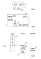
- FIG. 1 very schematically shows in the form of blocks an example of a simplified architecture of an integrated circuit 1, for example a smart card, of the type to which the present invention applies.
- the circuit 1 comprises a central processing unit 11 (CPU) associated with several memories 12 (MEM) among which at least one random access memory of the RAM type and a rewritable non-volatile memory, for example of the EEPROM type, and an input / output (I / O) circuit 13 allowing the exchange of data with the Outside the circuit 1.
- the different elements communicate by one or more internal buses 14 of data, addresses and commands.
- a category of attacks that can be made by fraudsters to obtain confidential data of the chip 1 relates to the so-called attacks by injection of faults. These attacks consist in disrupting the operation of component 1, for example, by means of radiation (laser, infrared, X-rays, etc.) or by other means (for example by acting on the power supply of the component) . In the case of data piracy, these attacks are generally iterative to successively discover the different bits of a secret quantity. Injections of fault usually cause a diversion in the course of a program. Such a trap can also be searched by a hacker, regardless of a data output to, for example, skip a protection mechanism, identification, etc.
- SPA simple power analysis
- Some integrated circuits include software and / or hardware tools to detect disturbances in their operation by verifying that a program has executed correctly. For example, we execute twice the same instructions and we check that they lead to the same result, or a signature calculation is performed on data extracted from the memory.
- the circuit includes light temperature detectors, etc. to detect a possible disturbance.
- FIG. 2 is a partial and very schematic representation of a conventional example of a mechanism of an integrated circuit 1 for protecting confidential data contained therein.
- the circuit 1 comprises one or more hardware detectors 21 (H DETECT) of the type of voltage, temperature, light sensor, etc. and / or one or more software detectors 22 (S DETECT) of the signature calculation type, calculation of a correction code, etc.
- the results of the detector (s) 21 and 22 are interpreted by a circuit or a program for monitoring the operation of the circuit (block 23, TRACK).
- the mechanism 23 causes either the writing (WR) of a control word (EEFLAG) in nonvolatile memory 121 (EEPROM), or the erasure (CLR) of this memory, at least for this which concerns the part containing data or secret algorithms of the circuit 1.
- WR writing
- EFLAG nonvolatile memory 121
- CLR erasure
- FIG. 3 illustrates the operation of the detection mechanism represented in FIG. 2.
- EXEC execution of a program 31 (PROGRAM) by the central unit (11, FIG. 1) of the integrated circuit
- FULT fault injection
- FAULT detection mechanism
- DETECT DETECT
- TRACK monitoring mechanism
- This detection leads to the processing of an alarm (block 23 ', ALARM) which causes writing or erasure (block 25, WR / CLR) in the non-volatile memory.
- a disadvantage of this kind of mechanism is that the current signature of a programming in a non-volatile EEPROM type memory is very characteristic and easy to detect by monitoring the consumption of the integrated circuit 1. Therefore, a fraudster who in parallel performs an analysis (ANALYSIS) of the circuit consumption is able to detecting, following its fault injection, the reaction of the circuit by an attempt to write to the non-volatile memory. The fraudster can then cause an immediate stop of the supply of the circuit (block 35, I DET / PW STOP) and thus prevent the execution of the countermeasure (block 25). Power failure can take various forms (for example, abrupt card output from a reader in the case of a smart card with contacts or removal of the remote power carrier in the case of a contactless card).
- the fraudster is able to suppress the power supply of the integrated circuit to prevent writing into the non-volatile memory or its erasure, it can re-iterate its attack by injecting faults and, for example, finish to obtain the digital quantity or quantities that are supposed to remain secret.
- the present invention aims to overcome all or part of the disadvantages of the known protection mechanisms of an integrated circuit following fault injection detection.
- the present invention more specifically aims at preventing a fraudster from preventing the execution of a write mechanism in non-volatile memory following detection of attempted fraud.
- the invention also aims to propose a solution compatible with the hardware elements of conventional integrated circuits.
- the invention also aims to propose a solution that applies regardless of the purpose of the fault injection (data output or simple diversion of a program).
- the intervention in non-volatile memory consists of copying information representative of the value of the variable of the volatile storage element into an area of the non-volatile memory.
- the method serves to protect the progress of a program executed by the integrated circuit.
- the content of said non-volatile memory information is tested to decide on the erasure of at least a part of this non-volatile memory.
- the method serves to protect a digital quantity contained in said non-volatile memory.
- the content of said non-volatile memory information conditions the data output of the integrated circuit.
- the intervention on the non-volatile memory is an at least partial erasure of this memory.
- the intervention on the non-volatile memory is performed periodically.
- said volatile storage element is a register of a central processing unit of the integrated circuit.
- said volatile storage element is an area of a volatile memory of the integrated circuit.
- the present invention also provides an integrated circuit comprising at least one central processing unit, a first non-volatile memory and a second volatile memory, at least one detector of an attempt to disturb the operation of the circuit, and such a protection mechanism.
- the present invention also provides a smart card, including such an integrated circuit.
- a characteristic of an embodiment of the present invention is, in the event of detection of a fault injection (whether intentional or accidental), of updating a variable in a volatile storage element of the circuit. integrated, then treat this information to copy in a non-volatile memory or erasure of at least the confidential data it contains, in a decorated manner of the detection.
- FIG. 4 partially shows, in a very schematic and block form, an embodiment of an integrated circuit 1 provided with a protection mechanism according to the present invention.
- the circuit 1 comprises one or more hardware detectors 21 (H DETECT) of possible disturbances on the operation of the integrated circuit or the execution of a program, and / or one or more software detectors 22 (S DETECT).
- H DETECT hardware detectors 21
- S DETECT software detectors 22
- TRACK hardware and / or software mechanism 43
- the mechanism 43 in the event of detection of a fault originating, for example, from an attempted fraud, causes the writing (WR) of a variable (FLAG) in a zone of volatile memory 122 (SRAM) of the integrated circuit 1.
- the recording of such a variable is not detectable on the consumption of the circuit insofar as it does not differ from normal and frequent program accesses in this memory nonvolatile.
- the variable FLAG is stored in a register of the central unit.
- the content of the FLAG variable in volatile memory is exploited on a regular basis, preferably periodically by means of a time counter (block 45, TIMER) of the central unit, for intervention on a rewritable non-volatile memory 121 (EEPROM).
- TIMER time counter
- EEPROM rewritable non-volatile memory
- an EEFLAG word is written (WR) in a zone (address) of the non-volatile memory 121.
- WR write
- a zone address
- the non-volatile memory 121 For example, it is a copy of the contents of the variable FLAG of memory 122.
- the FLAG variable of the volatile memory indicates the detection of an attempted fraud
- at least the area of the rewritable non-volatile memory 121 containing confidential data is erased (CLR).
- FIG. 5 very schematically illustrates a mode of operation of the mechanism described with reference to FIG. 4.
- the mechanism of the invention positions the FLAG variable (block 53, WR FLAG) in volatile memory.
- the protection mechanism of the invention (PROTECT) writes periodically (blocks 55, WR EEFLAG) the content (more generally, information representative of this content) of the variable FLAG of the volatile memory in a non-volatile memory. volatile.
- the periodicity (T) between two writes in non-volatile memory is preferably set by a counter of the central unit (not shown in FIG. 5).
- the management of the input / output (I / O) data of the integrated circuit depends on a reading (READ EEFLAG) of the zone containing the information EEFLAG in non-volatile memory, followed by a test (TEST) of the value of this information before deciding the output (OUTPUT) of data to the outside of the circuit.
- the period T between two writes of the EEFLAG information is then chosen to be less than the execution time of the program between a sensitive zone liable to a fault injection and the call to the entry procedure. output, so that you can avoid data output.
- the reading of the EEFLAG word in the non-volatile memory takes place before any operation considered to be sensitive from the point of view of the security of the execution of a program or of confidential data contained in the document. integrated circuit and, preferably, after each start of a new program session. If the value corresponds to an identified attack, the CPU causes, for example, erasure of the sensitive data in the nonvolatile memory, or prevents the program from starting.
- the content of the FLAG variable is chosen to have a balanced current signature between the indicator states of a fault detection and indicator of normal operation (identical Hamming weight of the two values).
- the address of the EEFLAG indicator word is not always the same.
- An advantage of the present invention is that it makes undetectable to a potential fraudster the fact that a fault injection attack has been detected by the circuit.
- Another advantage of the invention is that it preserves the non-volatile treatment of this fraud detection.
- Another advantage of the present invention is that it is compatible with the different modes of operation of fraud detection detections whether it is a prohibition of data output of a smart card or a card. deleting a memory area thereof.
- Another advantage of the present invention is that it does not modify the detection of a fraud attempt in itself and is compatible with conventional disturbance detectors.
Abstract
Description
La présente invention concerne de façon générale les circuits électroniques, et plus particulièrement, la protection du déroulement d'un programme exécuté par un circuit intégré ou de quantités numériques contenues dans un circuit intégré contre une extraction de ces données, suite à une perturbation du fonctionnement du circuit. L'invention concerne, par exemple, une protection contre une extraction de données suite à des injections de faute dans le fonctionnement du circuit et plus particulièrement dans un programme utilisant la ou les quantités numériques à protéger. Selon un autre exemple, l'invention concerne une protection contre une perturbation dans le déroulement d'un programme suite à une injection de faute.The present invention generally relates to electronic circuits, and more particularly, the protection of the progress of a program executed by an integrated circuit or of digital quantities contained in an integrated circuit against an extraction of these data, following a disturbance of the operation. of the circuit. The invention relates, for example, protection against data extraction following fault injections in the operation of the circuit and more particularly in a program using the digital quantity or quantities to be protected. According to another example, the invention relates to protection against a disturbance in the course of a program following a fault injection.
La présente invention s'applique, par exemple, aux cartes à puce.The present invention applies, for example, to smart cards.
La figure 1 représente, de façon très schématique et sous forme de blocs, un exemple d'architecture simplifiée d'un circuit intégré 1, par exemple d'une carte à puce, du type auquel s'applique la présente invention. Le circuit 1 comporte une unité centrale de traitement 11 (CPU) associé à plusieurs mémoires 12 (MEM) parmi lesquelles au moins une mémoire vive de type RAM et une mémoire non volatile réinscriptible, par exemple de type EEPROM, et un circuit 13 d'entrée-sortie (I/O) permettant l'échange de données avec l'extérieur du circuit 1. Les différents éléments communiquent par un ou plusieurs bus internes 14 de données, d'adresses et de commandes.FIG. 1 very schematically shows in the form of blocks an example of a simplified architecture of an
Une catégorie d'attaques susceptibles d'être effectuées par des fraudeurs pour obtenir des données confidentielles de la puce 1 concerne les attaques dites par injection de fautes. Ces attaques consistent à perturber le fonctionnement du composant 1, par exemple, au moyen d'un rayonnement (laser, infrarouge, rayons-X, etc.) ou par d'autres moyens (par exemple en agissant sur l'alimentation du composant). Dans le cas d'un piratage de données, ces attaques sont généralement itératives pour découvrir successivement les différents bits d'une quantité secrète. Les injections de faute provoquent généralement un déroutement dans le déroulement d'un programme. Un tel déroutement peut également être recherché par un pirate, indépendamment d'une sortie de données pour, par exemple, sauter un mécanisme de protection, d'identification, etc.A category of attacks that can be made by fraudsters to obtain confidential data of the
Ces attaques peuvent être combinées à une analyse de la consommation (SPA - Simple Power Analysis) qui consiste à mesurer la consommation énergétique du circuit intégré pendant l'exécution d'algorithmes manipulant des clés ou quantités secrètes que le fraudeur cherche à découvrir, cette consommation étant différente selon les états respectifs des bits des quantités manipulés. Les attaques par analyse statistique de la consommation sont basées sur l'exploitation de résultats fournis par le circuit à partir d'hypothèses faites sur les différents bits de la quantité à découvrir.These attacks can be combined with a simple power analysis (SPA) which consists of measuring the energy consumption of the integrated circuit during the execution of algorithms handling keys or secret quantities that the fraudster seeks to discover, this consumption. being different according to the respective states of the bits of the manipulated quantities. Attacks by statistical analysis of consumption are based on the exploitation of results provided by the circuit based on assumptions made on the different bits of the quantity to be discovered.
Certains circuits intégrés comprennent des outils logiciels et/ou matériels pour détecter des perturbations dans leur fonctionnement en vérifiant qu'un programme s'est exécuté correctement. Par exemple, on exécute deux fois les mêmes instructions et on vérifie qu'elles conduisent au même résultat, ou on effectue un calcul de signature sur des données extraites de la mémoire. Selon un autre exemple, le circuit comporte des détecteurs de température de lumière, etc. pour détecter une éventuelle perturbation.Some integrated circuits include software and / or hardware tools to detect disturbances in their operation by verifying that a program has executed correctly. For example, we execute twice the same instructions and we check that they lead to the same result, or a signature calculation is performed on data extracted from the memory. In another example, the circuit includes light temperature detectors, etc. to detect a possible disturbance.
La figure 2 représente, de façon partielle et très schématique, un exemple classique de mécanisme d'un circuit intégré 1 pour protéger des données confidentielles qu'il contient. Le circuit 1 comporte un ou plusieurs détecteurs matériels 21 (H DETECT) de type capteur de tension, de température, de lumière, etc. et/ou un ou plusieurs détecteurs logiciels 22 (S DETECT) de type calcul de signature, calcul d'un code correcteur, etc. Les résultats du ou des détecteurs 21 et 22 sont interprétés par un circuit ou un programme de surveillance du fonctionnement du circuit (bloc 23, TRACK). En cas de perturbation détectée, le mécanisme 23 provoque soit l'écriture (WR) d'un mot de contrôle (EEFLAG) en mémoire non volatile 121 (EEPROM), soit l'effacement (CLR) de cette mémoire, au moins pour ce qui concerne la partie contenant des données ou algorithmes secrets du circuit 1.FIG. 2 is a partial and very schematic representation of a conventional example of a mechanism of an integrated
La figure 3 illustre le fonctionnement du mécanisme de détection représenté en figure 2. Lors de l'exécution (EXEC) d'un programme 31 (PROGRAM) par l'unité centrale (11, figure 1) du circuit intégré, on suppose qu'un fraudeur perturbe le fonctionnement du circuit par une injection de faute (FAULT). Cette perturbation est détectée (bloc 20, DETECT) par le mécanisme de surveillance (TRACK) du fonctionnement du circuit. Cette détection conduit au traitement d'une alarme (bloc 23', ALARM) qui provoque l'écriture ou l'effacement (bloc 25, WR/CLR) dans la mémoire non volatile.FIG. 3 illustrates the operation of the detection mechanism represented in FIG. 2. During the execution (EXEC) of a program 31 (PROGRAM) by the central unit (11, FIG. 1) of the integrated circuit, it is assumed that a fraudster disrupts the operation of the circuit by fault injection (FAULT). This disturbance is detected (
Un inconvénient de ce genre de mécanisme est que la signature en courant d'une programmation dans une mémoire non volatile de type EEPROM est très caractéristique et facile à détecter en surveillant la consommation du circuit intégré 1. Par conséquent, un fraudeur qui en parallèle effectue une analyse (ANALYSIS) de la consommation du circuit est capable de détecter, suite à son injection de faute, la réaction du circuit par une tentative d'écriture dans la mémoire non volatile. Le fraudeur peut alors provoquer un arrêt immédiat de l'alimentation du circuit (bloc 35, I DET/PW STOP) et empêcher ainsi l'exécution de la contre mesure (bloc 25). La coupure de l'alimentation peut prendre différentes formes (par exemple, brusque sortie de la carte d'un lecteur en cas de carte à puce à contacts ou suppression de la porteuse de téléalimentation en cas de carte sans contact).A disadvantage of this kind of mechanism is that the current signature of a programming in a non-volatile EEPROM type memory is very characteristic and easy to detect by monitoring the consumption of the integrated
A partir du moment où le fraudeur est capable de supprimer l'alimentation du circuit intégré pour empêcher l'écriture dans la mémoire non volatile ou son effacement, il peut effectuer une nouvelle itération de son attaque par injection de fautes et, par exemple, finir par obtenir la ou les quantités numériques censées rester secrètes.From the moment the fraudster is able to suppress the power supply of the integrated circuit to prevent writing into the non-volatile memory or its erasure, it can re-iterate its attack by injecting faults and, for example, finish to obtain the digital quantity or quantities that are supposed to remain secret.
La présente invention vise à pallier tout ou partie des inconvénients des mécanismes connus de protection d'un circuit intégré suite à une détection d'injection de faute.The present invention aims to overcome all or part of the disadvantages of the known protection mechanisms of an integrated circuit following fault injection detection.
La présente invention vise plus particulièrement à éviter qu'un fraudeur puisse empêcher l'exécution d'un mécanisme d'écriture en mémoire non volatile suite à une détection de tentative de fraude.The present invention more specifically aims at preventing a fraudster from preventing the execution of a write mechanism in non-volatile memory following detection of attempted fraud.
L'invention vise également à proposer une solution compatible avec les éléments matériels des circuits intégrés classiques.The invention also aims to propose a solution compatible with the hardware elements of conventional integrated circuits.
L'invention vise également à proposer une solution qui s'applique quelque soit l'objectif de l'injection de faute (sortie de données ou simple déroutement d'un programme).The invention also aims to propose a solution that applies regardless of the purpose of the fault injection (data output or simple diversion of a program).
Pour atteindre tout ou partie de ces objets, la présente invention prévoit un procédé de protection d'un circuit intégré comportant au moins une mémoire non volatile, consistant à :
- détecter une éventuelle perturbation dans le déroulement d'un programme exécuté par le circuit intégré ;
- modifier la valeur d'une variable numérique dans un élément de mémorisation volatile en cas de détection de perturbation ; et
- de façon temporellement indépendante de la détection, intervenir sur la mémoire non volatile en fonction de la valeur de ladite variable.
- detect a possible disturbance in the course of a program executed by the integrated circuit;
- modifying the value of a numerical variable in a volatile storage element in the event of disturbance detection; and
- in a temporally independent manner of the detection, intervening on the non-volatile memory as a function of the value of said variable.
Selon un mode de mise en oeuvre de la présente invention, l'intervention en mémoire non volatile consiste à recopier une information représentative de la valeur de la variable de l'élément de mémorisation volatile dans une zone de la mémoire non volatile.According to an embodiment of the present invention, the intervention in non-volatile memory consists of copying information representative of the value of the variable of the volatile storage element into an area of the non-volatile memory.
Selon un mode de mise en oeuvre de la présente invention, le procédé sert à protéger le déroulement d'un programme exécuté par le circuit intégré.According to an embodiment of the present invention, the method serves to protect the progress of a program executed by the integrated circuit.
Selon un mode de mise en oeuvre de la présente invention, le contenu de ladite information en mémoire non volatile est testé pour décider de l'effacement d'au moins une partie de cette mémoire non volatile.According to an embodiment of the present invention, the content of said non-volatile memory information is tested to decide on the erasure of at least a part of this non-volatile memory.
Selon un mode de mise en oeuvre de la présente invention, le procédé sert à protéger une quantité numérique contenue dans ladite mémoire non volatile.According to an embodiment of the present invention, the method serves to protect a digital quantity contained in said non-volatile memory.
Selon un mode de mise en oeuvre de la présente invention, le contenu de ladite information en mémoire non volatile conditionne la sortie de données du circuit intégré.According to an embodiment of the present invention, the content of said non-volatile memory information conditions the data output of the integrated circuit.
Selon un mode de mise en oeuvre de la présente invention, l'intervention sur la mémoire non volatile est un effacement au moins partiel de cette mémoire.According to an embodiment of the present invention, the intervention on the non-volatile memory is an at least partial erasure of this memory.
Selon un mode de mise en oeuvre de la présente invention, l'intervention sur la mémoire non volatile est effectuée périodiquement.According to an embodiment of the present invention, the intervention on the non-volatile memory is performed periodically.
Selon un mode de mise en oeuvre de la présente invention, ledit élément de stockage volatil est un registre d'une unité centrale de traitement du circuit intégré.According to an embodiment of the present invention, said volatile storage element is a register of a central processing unit of the integrated circuit.
Selon un mode de mise en oeuvre de la présente invention, ledit élément de stockage volatil est une zone d'une mémoire volatile du circuit intégré.According to an embodiment of the present invention, said volatile storage element is an area of a volatile memory of the integrated circuit.
La présente invention prévoit également un circuit intégré comportant au moins une unité centrale de traitement, une première mémoire non volatile et une deuxième mémoire volatile, au moins un détecteur d'une tentative de perturbation du fonctionnement du circuit, et un tel mécanisme de protection.The present invention also provides an integrated circuit comprising at least one central processing unit, a first non-volatile memory and a second volatile memory, at least one detector of an attempt to disturb the operation of the circuit, and such a protection mechanism.
La présente invention prévoit également une carte à puce, comportant un tel circuit intégré.The present invention also provides a smart card, including such an integrated circuit.
Ces objets, caractéristiques et avantages, ainsi que d'autres de la présente invention seront exposés en détail dans la description suivante de modes de mise en oeuvre et de réalisation particuliers faite à titre non-limitatif en relation avec les figures jointes parmi lesquelles :
- la figure 1 qui a été décrite précédemment représente partiellement, de façon très schématique et sous forme de blocs, un exemple d'architecture d'un circuit intégré du type auquel s'applique la présente invention ;
- la figure 2 représente, de façon très schématique et sous forme de blocs, un mécanisme classique de protection d'un circuit intégré suite à la détection d'une injection de faute ;
- la figure 3 illustre le fonctionnement du mécanisme de la figure 2 ;
- la figure 4 représente, de façon très schématique et sous forme de blocs, un mode de réalisation d'un mécanisme de protection d'un circuit intégré selon la présente invention ; et
- la figure 5 illustre le fonctionnement du mécanisme de la figure 4.
- FIG. 1 which has been described above partially and very schematically shows in block form an exemplary architecture of an integrated circuit of the type to which the present invention applies;
- FIG. 2 very schematically shows, in the form of blocks, a conventional mechanism for protecting an integrated circuit following the detection of a fault injection;
- Figure 3 illustrates the operation of the mechanism of Figure 2;
- FIG. 4 very schematically shows in the form of blocks an embodiment of a protection mechanism of an integrated circuit according to the present invention; and
- FIG. 5 illustrates the operation of the mechanism of FIG. 4.
Les mêmes éléments ont été désignés par les mêmes références aux différentes figures. Pour des raisons de clarté, seuls les éléments et étapes de procédé qui sont utiles à la compréhension de l'invention ont été représentés aux figures et seront décrits par la suite. En particulier, la constitution logicielle ou matérielle des détecteurs de perturbations dans un circuit intégré n'a pas été détaillée, la présente invention étant compatible avec tout détecteur classique. De même, les programmes exécutés par un circuit intégré du type auquel s'applique l'invention et les données manipulées n'ont pas été exposés, l'invention étant là encore compatible avec tout programme classique.The same elements have been designated by the same references in the different figures. For the sake of clarity, only those elements and process steps that are useful for understanding the invention have been shown in the figures and will be described later. In particular, the constitution software or hardware of the disturbance detectors in an integrated circuit has not been detailed, the present invention being compatible with any conventional detector. Similarly, the programs executed by an integrated circuit of the type to which the invention applies and the data manipulated have not been exposed, the invention being again compatible with any conventional program.
Une caractéristique d'un mode de mise en oeuvre de la présente invention est, en cas de détection d'une injection de faute (qu'elle soit volontaire ou accidentelle), de mettre à jour une variable dans un élément de stockage volatil du circuit intégré, puis de traiter cette information pour recopie dans une mémoire non volatile ou effacement d'au moins les données confidentielles qu'elle contient, de façon décorélée de la détection.A characteristic of an embodiment of the present invention is, in the event of detection of a fault injection (whether intentional or accidental), of updating a variable in a volatile storage element of the circuit. integrated, then treat this information to copy in a non-volatile memory or erasure of at least the confidential data it contains, in a decorated manner of the detection.
La figure 4 représente, partiellement, de façon très schématique et sous forme de blocs, un mode de réalisation d'un circuit intégré 1 pourvu d'un mécanisme de protection selon la présente invention.FIG. 4 partially shows, in a very schematic and block form, an embodiment of an
Comme précédemment, le circuit 1 comporte un ou plusieurs détecteurs matériels 21 (H DETECT) d'éventuelles perturbations sur le fonctionnement du circuit intégré ou l'exécution d'un programme, et/ou un ou plusieurs détecteurs logiciels 22 (S DETECT). Les résultats de ces détecteurs sont exploités par un mécanisme matériel et/ou logiciel 43 (TRACK).As before, the
Selon ce mode de réalisation de l'invention, en cas de détection d'une faute provenant, par exemple, d'une tentative de fraude, le mécanisme 43 provoque l'écriture (WR) d'une variable (FLAG) dans une zone de mémoire volatile 122 (SRAM) du circuit intégré 1. L'enregistrement d'une telle variable n'est pas détectable sur la consommation du circuit dans la mesure où elle ne se différencie pas d'accès normaux et fréquents du programme dans cette mémoire non volatile. En variante, la variable FLAG est stockée dans un registre de l'unité centrale.According to this embodiment of the invention, in the event of detection of a fault originating, for example, from an attempted fraud, the
Le contenu de la variable FLAG en mémoire volatile est exploité de façon régulière, de préférence de façon périodique au moyen d'un compteur temporel (bloc 45, TIMER) de l'unité centrale, pour intervention sur une mémoire non volatile réinscriptible 121 (EEPROM).The content of the FLAG variable in volatile memory is exploited on a regular basis, preferably periodically by means of a time counter (block 45, TIMER) of the central unit, for intervention on a rewritable non-volatile memory 121 (EEPROM).
Selon un premier mode de mise en oeuvre de l'invention, un mot EEFLAG est écrit (WR) dans une zone (adresse) de la mémoire non volatile 121. Par exemple, il s'agit d'une recopie du contenu de la variable FLAG de la mémoire 122.According to a first embodiment of the invention, an EEFLAG word is written (WR) in a zone (address) of the
Selon un autre mode de mise en oeuvre, si la variable FLAG de la mémoire volatile indique la détection d'une tentative de fraude, au moins la zone de la mémoire non volatile réinscriptible 121 contenant des données confidentielles est effacée (CLR).According to another embodiment, if the FLAG variable of the volatile memory indicates the detection of an attempted fraud, at least the area of the rewritable
La figure 5 illustre, de façon très schématique, un mode de fonctionnement du mécanisme décrit en relation avec la figure 4.FIG. 5 very schematically illustrates a mode of operation of the mechanism described with reference to FIG. 4.
On suppose une exécution (EXEC) d'un programme 31 (PROGRAM) et l'injection d'une faute (FAULT) dans son déroulement.We assume an execution (EXEC) of a program 31 (PROGRAM) and the injection of a fault (FAULT) in its course.
Comme précédemment, cette faute est détectée (bloc 20, DETECT) par le mécanisme (TRACK) de surveillance du fonctionnement du circuit 1.As before, this fault is detected (block 20, DETECT) by the mechanism (TRACK) for monitoring the operation of
Suite à cette détection, le mécanisme de l'invention positionne la variable FLAG (bloc 53, WR FLAG) en mémoire volatile.Following this detection, the mechanism of the invention positions the FLAG variable (block 53, WR FLAG) in volatile memory.
Parallèlement et de façon indépendante, le mécanisme de protection de l'invention (PROTECT) écrit périodiquement (blocs 55, WR EEFLAG) le contenu (plus généralement, une information représentative de ce contenu) de la variable FLAG de la mémoire volatile en mémoire non volatile. La périodicité (T) entre deux écritures en mémoire non volatile est fixée, de préférence, par un compteur de l'unité centrale (non représentée en figure 5).In parallel and independently, the protection mechanism of the invention (PROTECT) writes periodically (blocks 55, WR EEFLAG) the content (more generally, information representative of this content) of the variable FLAG of the volatile memory in a non-volatile memory. volatile. The periodicity (T) between two writes in non-volatile memory is preferably set by a counter of the central unit (not shown in FIG. 5).
Dans l'exemple illustré par la figure 5, la gestion des entrées-sorties (I/O) de données du circuit intégré dépend d'une lecture (READ EEFLAG) de la zone contenant l'information EEFLAG en mémoire non volatile, suivi d'un test (TEST) de la valeur de cette information avant de décider de la sortie (OUTPUT) de données vers l'extérieur du circuit. De préférence, la période T entre deux écritures de l'information EEFLAG est alors choisie pour être inférieure à la durée d'exécution du programme entre une zone sensible susceptible de subir une injection de faute et l'appel à la procédure d'entrée-sortie, de façon à pouvoir éviter la sortie de données.In the example illustrated in FIG. 5, the management of the input / output (I / O) data of the integrated circuit depends on a reading (READ EEFLAG) of the zone containing the information EEFLAG in non-volatile memory, followed by a test (TEST) of the value of this information before deciding the output (OUTPUT) of data to the outside of the circuit. Preferably, the period T between two writes of the EEFLAG information is then chosen to be less than the execution time of the program between a sensitive zone liable to a fault injection and the call to the entry procedure. output, so that you can avoid data output.
Selon un autre mode de mise en oeuvre, la lecture du mot EEFLAG dans la mémoire non volatile s'effectue avant toute opération considérée comme sensible du point de vue de la sécurité de l'exécution d'un programme ou de données confidentielles contenues dans le circuit intégré et, de préférence, après chaque démarrage d'une nouvelle session de programme. Si la valeur correspond à une attaque identifiée, l'unité centrale provoque, par exemple, l'effacement des données sensibles dans la mémoire non volatile, ou empêche le démarrage du programme.According to another embodiment, the reading of the EEFLAG word in the non-volatile memory takes place before any operation considered to be sensitive from the point of view of the security of the execution of a program or of confidential data contained in the document. integrated circuit and, preferably, after each start of a new program session. If the value corresponds to an identified attack, the CPU causes, for example, erasure of the sensitive data in the nonvolatile memory, or prevents the program from starting.
De préférence, le contenu de la variable FLAG est choisi pour avoir une signature en courant équilibrée entre les états indicateurs d'une détection de faute et indicateur d'un fonctionnement normal (poids de Hamming identique des deux valeurs).Preferably, the content of the FLAG variable is chosen to have a balanced current signature between the indicator states of a fault detection and indicator of normal operation (identical Hamming weight of the two values).
De préférence, afin de préserver la durée de vie de la mémoire non volatile de type EEPROM, l'adresse du mot indicateur EEFLAG n'est pas toujours la même.Preferably, in order to preserve the lifetime of the nonvolatile EEPROM memory, the address of the EEFLAG indicator word is not always the same.
Un avantage de la présente invention est qu'elle rend indétectable à un fraudeur éventuel le fait qu'une attaque par injection de faute ait été détectée par le circuit.An advantage of the present invention is that it makes undetectable to a potential fraudster the fact that a fault injection attack has been detected by the circuit.
Un autre avantage de l'invention est qu'elle préserve le traitement non volatile de cette détection de fraude.Another advantage of the invention is that it preserves the non-volatile treatment of this fraud detection.
Un autre avantage de la présente invention est qu'elle est compatible avec les différents modes d'exploitation des détections des tentatives de fraude qu'il s'agisse d'une interdiction de sortie de données d'une carte à puce ou d'un effacement d'une zone mémoire de celle-ci.Another advantage of the present invention is that it is compatible with the different modes of operation of fraud detection detections whether it is a prohibition of data output of a smart card or a card. deleting a memory area thereof.
Un autre avantage de la présente invention est qu'elle ne modifie pas la détection d'une tentative de fraude en elle-même et est compatible avec les détecteurs de perturbation classiques.Another advantage of the present invention is that it does not modify the detection of a fraud attempt in itself and is compatible with conventional disturbance detectors.
Bien entendu, la présente invention est susceptible de diverses variantes et modifications qui apparaîtront à l'homme de l'art. En particulier, la mise en oeuvre pratique de l'invention par des moyens logiciels et/ou matériels est à la portée de l'homme de métier à partir des indications fonctionnelles données ci-dessus. De plus, bien que l'invention ait été décrite en relation avec une application préférée aux cartes à puce, elle s'applique plus généralement à la protection de n'importe quel circuit intégré.Of course, the present invention is susceptible of various variations and modifications which will be apparent to those skilled in the art. In particular, the practical implementation of the invention by software and / or hardware means is within the abilities of those skilled in the art from the functional indications given above. In addition, although the invention has been described in relation to a preferred application to smart cards, it more generally applies to the protection of any integrated circuit.
Claims (12)
Applications Claiming Priority (1)
| Application Number | Priority Date | Filing Date | Title |
|---|---|---|---|
| FR0551011 | 2005-04-21 |
Publications (2)
| Publication Number | Publication Date |
|---|---|
| EP1715436A2 true EP1715436A2 (en) | 2006-10-25 |
| EP1715436A3 EP1715436A3 (en) | 2007-03-28 |
Family
ID=34980022
Family Applications (1)
| Application Number | Title | Priority Date | Filing Date |
|---|---|---|---|
| EP06112843A Withdrawn EP1715436A3 (en) | 2005-04-21 | 2006-04-20 | Protection of program execution performed by an integrated circuit or the data stored in this circuit |
Country Status (2)
| Country | Link |
|---|---|
| US (1) | US7593258B2 (en) |
| EP (1) | EP1715436A3 (en) |
Families Citing this family (4)
| Publication number | Priority date | Publication date | Assignee | Title |
|---|---|---|---|---|
| FR2915007A1 (en) * | 2007-04-12 | 2008-10-17 | St Microelectronics Sa | PROTECTION OF THE EXECUTION OF A PROGRAM |
| FR2924262B1 (en) * | 2007-11-26 | 2009-12-11 | Sagem Securite | METHOD OF MASKING A PASSAGE AT THE END OF LIFE OF AN ELECTRONIC DEVICE AND DEVICE COMPRISING A CORRESPONDING CONTROL MODULE |
| KR101269549B1 (en) * | 2009-05-08 | 2013-06-04 | 한국전자통신연구원 | System and method for testing software reliability using fault injection |
| US9122605B2 (en) * | 2013-09-23 | 2015-09-01 | Honeywell International Inc. | Methods for determining multiple simultaneous fault conditions |
Citations (2)
| Publication number | Priority date | Publication date | Assignee | Title |
|---|---|---|---|---|
| US5465349A (en) * | 1990-10-19 | 1995-11-07 | Gemplus Card International | System for monitoring abnormal integrated circuit operating conditions and causing selective microprocessor interrupts |
| DE10303752A1 (en) | 2003-01-30 | 2004-08-19 | Infineon Technologies Ag | Memory management or control arrangement, especially for a chip card, wherein data can be written back to main memory from cache memory independently of any displacement of data from cache memory |
Family Cites Families (8)
| Publication number | Priority date | Publication date | Assignee | Title |
|---|---|---|---|---|
| CA2350029A1 (en) * | 2001-06-08 | 2002-12-08 | Cloakware Corporation | Sustainable digital watermarking via tamper-resistant software |
| US6778066B2 (en) * | 2001-06-29 | 2004-08-17 | Hewlett-Packard Development Company, L.P. | Personal identification badge that resets on the removal of the badge from the wearer |
| AU2002344652A1 (en) | 2002-07-17 | 2004-02-02 | Etsuro Sakagami | Filtration method, filtration device, method of desalinating sea water by using the device, and method of desulfurizing petroleum |
| EP1383047A1 (en) * | 2002-07-18 | 2004-01-21 | Cp8 | Method for the secure execution of a program against attacks by radiation or other means |
| FR2855286B1 (en) * | 2003-05-22 | 2005-07-22 | Gemplus Card Int | SECURE TRANSMISSION OF DATA BETWEEN TWO MODULES |
| FR2884000A1 (en) * | 2005-04-05 | 2006-10-06 | St Microelectronics Sa | Cryptographic coprocessor control execution monitoring method for integrated circuit, involves carrying error signal if abnormal flow of execution is detected and preventing access to register as long as signal is given with active value |
| US7372304B2 (en) * | 2005-10-04 | 2008-05-13 | Stmicroelectronics, Inc. | System and method for glitch detection in a secure microcontroller |
| US7769165B2 (en) * | 2005-10-14 | 2010-08-03 | Microsoft Corporation | Semi-public white-box cipher |
-
2006
- 2006-04-20 EP EP06112843A patent/EP1715436A3/en not_active Withdrawn
- 2006-12-19 US US11/641,550 patent/US7593258B2/en active Active
Patent Citations (2)
| Publication number | Priority date | Publication date | Assignee | Title |
|---|---|---|---|---|
| US5465349A (en) * | 1990-10-19 | 1995-11-07 | Gemplus Card International | System for monitoring abnormal integrated circuit operating conditions and causing selective microprocessor interrupts |
| DE10303752A1 (en) | 2003-01-30 | 2004-08-19 | Infineon Technologies Ag | Memory management or control arrangement, especially for a chip card, wherein data can be written back to main memory from cache memory independently of any displacement of data from cache memory |
Non-Patent Citations (1)
| Title |
|---|
| HAGAI BAR-EL, THE SORCERER'S APPRENTICE GUIDE TO FAULT ATTACKS, 7 May 2004 (2004-05-07) |
Also Published As
| Publication number | Publication date |
|---|---|
| US7593258B2 (en) | 2009-09-22 |
| US20070159882A1 (en) | 2007-07-12 |
| EP1715436A3 (en) | 2007-03-28 |
Similar Documents
| Publication | Publication Date | Title |
|---|---|---|
| CA2053741C (en) | Access security integrated circuit | |
| JP3941964B2 (en) | Method and apparatus for protecting data stored in a semiconductor memory cell | |
| EP1712976B1 (en) | Protection of data in a memory associated with a microprocessor | |
| EP2162846B1 (en) | Cryptoprocessor with improved data protection | |
| FR2938358A1 (en) | SECURE MEMORY INTERFACE | |
| EP1904946B1 (en) | Detection of faults during a long perturbation | |
| US8997255B2 (en) | Verifying data integrity in a data storage device | |
| FR2977694A1 (en) | MICROPROCESSOR PROTECTS AGAINST A BATTERY OVERFLOW | |
| EP1602024A1 (en) | Secure computer data storage method and device | |
| FR2894709A1 (en) | "DETECTOR OF ABNORMAL DESTRUCTION OF MEMORY SECTOR" | |
| FR2810152A1 (en) | EEPROM for securing electronic devices such as chip cards has elements for detection and correction of memory errors within the secure non-erasable memory area | |
| EP1715436A2 (en) | Protection of program execution performed by an integrated circuit or the data stored in this circuit | |
| US20190080111A1 (en) | Method for protecting unauthorized data access from a memory | |
| FR2923923A1 (en) | CHECKING DATA IN MEMORY | |
| EP1006532B1 (en) | Secure EEPROM with UV erasure detection means | |
| FR2889005A1 (en) | PERMANENT MATERIAL INTEGRITY OF DATA | |
| EP3637266A1 (en) | Method for accessing a memory | |
| EP1603138A1 (en) | Non-volatile memory with memory cell reading falsifying means | |
| EP1717704A2 (en) | Protection of program execution performed by an integrated circuit | |
| EP1818846B1 (en) | Verification of the integrity of programs or of sequencing in a state machine | |
| EP1713023A1 (en) | Protection of data contained in an integrated circuit | |
| EP2860669B1 (en) | Method implemented in a microcircuit and related device | |
| FR2926381A1 (en) | METHOD OF SECURE TRANSFER OF DATA | |
| EP2104893A2 (en) | Secured electronic systems, securing methods and uses of such systems | |
| FR3011650A1 (en) | METHOD AND DEVICE FOR REALIZING FUNCTION BY A MICROCIRCUIT |
Legal Events
| Date | Code | Title | Description |
|---|---|---|---|
| PUAI | Public reference made under article 153(3) epc to a published international application that has entered the european phase |
Free format text: ORIGINAL CODE: 0009012 |
|
| AK | Designated contracting states |
Kind code of ref document: A2 Designated state(s): AT BE BG CH CY CZ DE DK EE ES FI FR GB GR HU IE IS IT LI LT LU LV MC NL PL PT RO SE SI SK TR |
|
| AX | Request for extension of the european patent |
Extension state: AL BA HR MK YU |
|
| PUAL | Search report despatched |
Free format text: ORIGINAL CODE: 0009013 |
|
| AK | Designated contracting states |
Kind code of ref document: A3 Designated state(s): AT BE BG CH CY CZ DE DK EE ES FI FR GB GR HU IE IS IT LI LT LU LV MC NL PL PT RO SE SI SK TR |
|
| AX | Request for extension of the european patent |
Extension state: AL BA HR MK YU |
|
| 17P | Request for examination filed |
Effective date: 20070927 |
|
| 17Q | First examination report despatched |
Effective date: 20071029 |
|
| AKX | Designation fees paid |
Designated state(s): DE FR GB IT |
|
| STAA | Information on the status of an ep patent application or granted ep patent |
Free format text: STATUS: THE APPLICATION IS DEEMED TO BE WITHDRAWN |
|
| 18D | Application deemed to be withdrawn |
Effective date: 20111101 |