EP1711039A1 - Multi-phase input ballast - Google Patents
Multi-phase input ballast Download PDFInfo
- Publication number
- EP1711039A1 EP1711039A1 EP06005749A EP06005749A EP1711039A1 EP 1711039 A1 EP1711039 A1 EP 1711039A1 EP 06005749 A EP06005749 A EP 06005749A EP 06005749 A EP06005749 A EP 06005749A EP 1711039 A1 EP1711039 A1 EP 1711039A1
- Authority
- EP
- European Patent Office
- Prior art keywords
- circuit
- signal
- power
- lamp
- voltage
- Prior art date
- Legal status (The legal status is an assumption and is not a legal conclusion. Google has not performed a legal analysis and makes no representation as to the accuracy of the status listed.)
- Withdrawn
Links
Images


Classifications
-
- H—ELECTRICITY
- H05—ELECTRIC TECHNIQUES NOT OTHERWISE PROVIDED FOR
- H05B—ELECTRIC HEATING; ELECTRIC LIGHT SOURCES NOT OTHERWISE PROVIDED FOR; CIRCUIT ARRANGEMENTS FOR ELECTRIC LIGHT SOURCES, IN GENERAL
- H05B41/00—Circuit arrangements or apparatus for igniting or operating discharge lamps
- H05B41/14—Circuit arrangements
- H05B41/36—Controlling
- H05B41/38—Controlling the intensity of light
- H05B41/39—Controlling the intensity of light continuously
- H05B41/392—Controlling the intensity of light continuously using semiconductor devices, e.g. thyristor
- H05B41/3921—Controlling the intensity of light continuously using semiconductor devices, e.g. thyristor with possibility of light intensity variations
- H05B41/3925—Controlling the intensity of light continuously using semiconductor devices, e.g. thyristor with possibility of light intensity variations by frequency variation
-
- H—ELECTRICITY
- H02—GENERATION; CONVERSION OR DISTRIBUTION OF ELECTRIC POWER
- H02J—CIRCUIT ARRANGEMENTS OR SYSTEMS FOR SUPPLYING OR DISTRIBUTING ELECTRIC POWER; SYSTEMS FOR STORING ELECTRIC ENERGY
- H02J3/00—Circuit arrangements for ac mains or ac distribution networks
- H02J3/007—Arrangements for selectively connecting the load or loads to one or several among a plurality of power lines or power sources
-
- H—ELECTRICITY
- H05—ELECTRIC TECHNIQUES NOT OTHERWISE PROVIDED FOR
- H05B—ELECTRIC HEATING; ELECTRIC LIGHT SOURCES NOT OTHERWISE PROVIDED FOR; CIRCUIT ARRANGEMENTS FOR ELECTRIC LIGHT SOURCES, IN GENERAL
- H05B41/00—Circuit arrangements or apparatus for igniting or operating discharge lamps
- H05B41/14—Circuit arrangements
- H05B41/36—Controlling
- H05B41/38—Controlling the intensity of light
- H05B41/39—Controlling the intensity of light continuously
- H05B41/392—Controlling the intensity of light continuously using semiconductor devices, e.g. thyristor
- H05B41/3921—Controlling the intensity of light continuously using semiconductor devices, e.g. thyristor with possibility of light intensity variations
- H05B41/3924—Controlling the intensity of light continuously using semiconductor devices, e.g. thyristor with possibility of light intensity variations by phase control, e.g. using a triac
Definitions
- the present invention relates to dimmable ballasts for discharge lamps.
- the invention relates to a method and apparatus for powering a dimmable ballast from a multi-phase power source.
- Fluorescent lamps also known as gas discharge lamps
- Fluorescent lamps economically illuminate an area. Due to the unique operating characteristics of fluorescent lamps, the lamps must be powered by a ballast. Electronic ballasts provide a very efficient method of powering fluorescent lamps and for adjusting the illumination level of fluorescent lamps.
- an electronic ballast is driven by a single AC (alternating current) voltage supply having a particular phase.
- the electronic ballast typically has a boost front-end for converting the AC voltage from an AC power source into a DC (direct current) voltage which has a value greater than the peak voltage of the AC power source.
- An inverter then converts the DC voltage into high frequency AC power.
- dimming ballasts be capable of being powered from a multi-phase input. More specifically, it is desirable to have an electronic ballast that can be driven by two different AC voltages supplies supplying AC voltages at different phases.
- a ballast circuit for connection to a first alternating current (AC) source having a first phase and to a second AC source having a second phase.
- the ballast includes a first switching circuit for selectively receiving the first AC source and a second switching circuit for selectively receiving the second AC source.
- the circuit further includes a control circuit for controlling the first and second switching circuits to provide power from one of the first and second AC sources to the lamp via a rectifier and power factor correction and inverter circuits.
- a method for powering a lamp connected to a ballast circuit.
- the method includes supplying a first input signal and a second input signal to the ballast.
- the method further includes generating first and a second complimentary control signals.
- the method also includes providing power from one of the first and second input signals to lamp (via a rectifier and power factor correction and inverter circuits) as a function of the first and second control signals.
- a method for powering a lamp connected to a ballast.
- the method includes receiving a first alternating current (AC) voltage via a first switching circuit.
- the method also includes receiving a second AC voltage to via a second switching circuit.
- the method further includes selectively controlling the first and second switching circuits to provide one of the first and second AC voltages to power the lamp via a rectifier and power factor correction and inverter circuits.
- AC alternating current
- the invention may comprise various other methods and apparatuses.
- FIG. 1A is a block diagram illustrating a multi-phase input dimming ballast circuit for powering a lamp according to one preferred embodiment of the invention.
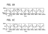
- FIGS. 1B and 1C illustrate exemplary waveforms of AC voltage signals produced by AC voltage sources and provided as inputs to the triacs according to one preferred embodiment of the invention.
- FIGS. 1D and 1E illustrate exemplary waveforms of AC voltage signals output from first and second triacs according to one preferred embodiment of the invention.
- FIGS. IF illustrates exemplary waveforms of an output voltage signal produced by a pulse generator according to one preferred embodiment of the invention.
- FIG. 1G illustrates exemplary threshold voltage signals applied to first and second triacs to generate the exemplary waveforms shown in FIGS 1D and 1E.
- FIG. 2 is a schematic diagram illustrating the components of a control circuit according to one preferred embodiment of the invention.
- FIG. 3 is a schematic diagram illustrating the components of a multi-source detector according to one preferred embodiment of the invention.
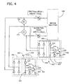
- FIG. 4 is a schematic diagram illustrates the components of first and second 15 volt DC voltage circuits according to one embodiment of the invention.
- FIG. 1A is a block diagram of an embodiment of a multi-phase input dimming ballast 100 for powering a lamp 102.
- the ballast 100 receives power from a first AC power source 104 via power lines 106 and 108 and from a second AC power source 110 via power lines 112 and 108.
- the first AC power source 104 supplies a first AC voltage signal 109 (see FIG. 1B) having a particular phase via power lines 106 and 108
- the second AC power source 110 supplies a second AC voltage signal 111 (see FIG. 1C) having a different phase via power lines 112 and 108.
- the power lines 106 and 112 may be referred to as either “HOT” or “SUPPLY” and power line 108 may be referred to as "NEUTRAL” or “COMMON.”
- the first and second AC voltage signals 109, 111 may have different phases; they generally have substantially the same voltage magnitude.
- FIGS. 1B and 1C show example waveforms of AC voltage signals 109, 111 produced by the first and second AC sources 104, 110, respectively. In this example, the phases of the signals are shifted approximately 90 degrees.
- a first triac 116 is coupled to the AC power line 106 and outputs a first output AC voltage signal 113 for powering the lamp 102 via a rectifier 136 and power factor correction and inverter circuits 138.
- a second triac 118 is coupled to the AC power line 112 and outputs a second output AC voltage signal 115 for powering the lamp 102 via rectifier 136 and power factor correction and inverter circuits 138.
- Each of the first and second triacs 116, 118 have conduction terminals 120,122 and a gate terminal 124. Terminals 120 of the first triac 116 and the second triac 118 are coupled to AC power lines 106, 112, respectively.
- a threshold voltage In order for triacs 116, 118 to output the first and second voltage signal 113, 115 between terminals 120 and 122, a threshold voltage must be applied to the gate terminal 124.
- each of the triacs 116, 118 conducts for at least a full peak current (I/P) cycle of the corresponding AC signal or a few I/P cycles when the threshold voltage is applied to gate 124.
- the threshold voltage is applied to the triacs 116, 118 in an alternating fashion such that only one of the triacs 116. 118 conducts at a particular instant in time.
- a first triac driver/zero crossing detector (ZCD) component 126 is coupled to the gate terminal 124 of the first triac 116 and supplies the required threshold voltage to activate the first triac 116.
- a second triac driver/zero crossing detector (ZCD) component 128 is coupled to the gate terminal 124 of the second triac 118 and supplies the required threshold voltage to activate the second triac 118.
- the first AC voltage signal is conducted from terminal 120 to terminal 122 of the first triac 116 when the first triac 116 is activated
- the second AC voltage signal is conducted from terminal 120 to terminal 122 of the second triac 118 when the second triac 118 is activated.
- the purpose of the ZCD portion of the first and second triac driver/zero crossing detector (ZCD) components 126, 128 is to fire the triacs 116,118 at the zero crossing of the AC I/P voltage signals 109 and 111. (See FIGS. 1B and I C).
- a control circuit 130 is coupled to the first and second triac driver/ZCD components 126, 128 and controls the first triac driver/ZCD 126 and the second triac driver/ZCD component 128 to alternatively provide the required threshold voltage to gate terminal 124 of the first and second triacs 116, 118, respectively.
- the control circuit 130 controls which one of the triacs 116, 118 will conduct during a given period of time.
- the control circuit 130 is configured to generate a first control signal 132 and a second control signal 134.
- the first and second control signals 132, 134 are complimentary in nature.
- the first control signal 132 has a first state when the second control signal has a second state, and the first control signal 132 has the second state when the second control signal has the first state.
- the first control signal 132 has a peak magnitude (e.g., five volts)
- the second control signal 134 has a minimum magnitude (e.g., 0 volts)
- the first control signal 132 has the minimum magnitude the second control signal 134 has the peak magnitude (e.g. five volts).
- FIGS. 1D and 1E show example waveforms of the output AC voltage signals 113, 115 as produced by the first and second traics 116, 118, respectively. As it can be seen, the first and second output AC voltage signals 113, 115 are also complimentary.
- the first triac 116 outputs the first output signal 113, and the second triac 118 does not produce an output signal.
- T 3 as indicated by reference character 137, the second triac 118 outputs the second output signal 115, and the first triac 116 does not conduct an output signal.
- a bridge rectifier 136 is coupled to the common line 108 and the terminal 122 of the first triac 116 to convert the first AC voltage signal output from the first triac 116 to a DC voltage signal, for application to a power factor correction (PFC)/inverter circuit 138 coupled thereto via lines 117 and 119.
- the bridge rectifier 136 is coupled to the common line 108 and the terminal 122 of the second triac 118 to convert the second AC voltage signal output from the second triac 118 to a DC voltage signal for application to the factor PFC/inverter circuit 138 via lines 117 and 119.
- the DC voltage signal applied to the PFC/inverter circuit 138 is a function of the first output AC voltage signal 113
- the second triac 118 conducts
- the DC voltage signal applied to the PFC/inverter circuit 138 is a function of the second output AC voltage signal 115.
- the bridge rectifier 136 converts each of the first and second output AC voltage signals 113, 15 into DC voltage signals having approximately the same magnitude.
- the PFC/inverter circuit 138 controls the powering of the lamp 102 based upon power received from the rectifier 136 and a dim level command signal 140 received from a dimming regulation circuit 142.
- the PFC/inverter circuit 138 is configured to insure a high power factor and low current total harmonic distortion. The detailed operation of the PFC/inverter circuit 138 and is explained in greater detail in commonly owned U.S. Patent 6,486,616 , the disclosure of which is incorporated herein by reference.
- a multi-source detection circuit 144 is coupled to the first AC power source 104 via power line 106 and coupled to the second AC power source 110 via power line 112.
- the multi-source detection circuit 144 generates a detection signal 146 that indicates whether one or both of the first and second AC voltage signals are being supplied to the ballast 100. For example, when both signals are being supplied, the multi-source detection circuit 144 generates a detection signal 146 having a low voltage magnitude (e.g., 0 volts). Alternatively, when at least one of the first and second AC voltage signals is absent (e.g., one source turned-off), the multi-source detection circuit 144 generates a detection 146 signal having a high voltage magnitude (e.g., 5 volts).
- control circuit 130 is responsive to an "off" state of one of the first or second AC sources for controlling the operation of the first and second triac driver/ZCD components 126, 128.
- the control circuit will control triac driver/ZCD components such that power is continuously supplied from the AC voltage source in an "on" state.
- the detection signal 146 can be provided to a dimming regulation circuit 142 to cause dimming of the lamp 102.
- the dimming regulation circuit 142 is responsive to the detection signal 146 to generate the dim level command signal 140 as a function of the amplitude of the detection signal 146.
- the amplitude of the dim level command signal 140 determines the inverter running frequency, and the inverter running frequency determines whether dimming of the lamp 102 occurs. For example, when one of the first or second AC sources is turned off, the detection signal 146 will have a peak magnitude. This change in status of the detection signal 146 will cause the dimming regulation circuit 142 to generate a dim level command signal 140 that causes an increase in the inverter running frequency.
- the detection signal 146 will have a peak amplitude and, thus, the dim level command signal 140 generated by the dimming regulation circuit 142 will have a peak amplitude.
- the inverter 138 is responsive to a dim level command signal 140 having a peak amplitude to operate at a increased frequency. Due to the increased operating frequency, the inverter 138 will provide an output signal 153 (i.e., lamp current) having a lower amplitude, causing the lamp 102 to dim.
- the detection signal 146 When both of the first and second AC sources 104, 110 are turned on, the detection signal 146 will have a minimum amplitude and the dim level command signal 140 generated by the dimming regulation circuit 142 will also have a minimum amplitude.
- the inverter 138 is responsive to a dim level command signal 140 having the minimum amplitude to operate at normal frequency. When operating at the normal frequency, the inverter 138 will provide an output signal 153 (i.e., lamp current) having a higher amplitude, causing the lamp 102 to brighten (i.e., to operate in a full light, or non-dimming, mode).
- the dimming regulation circuit 142 operates to reduce the power applied to the lamp 102 when one of the AC sources 104, 110 is not generating an AC signal.
- the control circuit 130 comprises a pulse generator 202, a first optocoupler 204, a second optocoupler 206, and a transistor 208.
- the pulse generator 202 preferably comprises an 8-pin integrated circuit such as a LM555 timer manufactured by National Semiconductor Corporation of Santa Clara, California, USA.
- the pulse generator 202 generates a pulsed output voltage signal 209 having two states that correspond to an on time and an off time. Power is supplied to the pulse generator 202 by a first DC voltage supply 210 (e.g., 15V) generated from the second AC voltage source (see FIG. 4).
- the first and second optocouplers 204, 206 each include an anode 212, a cathode 214, a collector 216, and an emitter 218.
- the emitter 218 of each of the first and second optocouplers 204, 206 is coupled to ground.
- the cathode 214 of the second optocoupler 206 is also coupled to ground.
- the first DC power supply 210 is coupled to the collector 216 of the second optocoupler 206 via resistor 219.
- a second DC power supply 220 is coupled to the collector 216 of the first optocoupler 204 via a resistor 233, to the second triac driver 222 (e.g., triac driver 128) via resistor 233, and to the anode 212 of the second optocoupler 206 via resistor 235.
- a collector 226 of the transistor 208 is coupled to an input (e.g. pin 6) of pulse generator 202.
- the emitter 228 of the transistor 208 is coupled to a different input (e.g., pin 7) of the pulse generator 202 via a capacitor 230 and a resistor 232 and to the cathode 214 of the first optocoupler 204.
- a first triac driver 234 (e.g., triac driver 126) is coupled to the pulse generator 202 and receives the pulsed output signal 209.
- the pulsed output signal 209 controls the first triac driver 234 to turn the first triac 126 on and off.
- the anode 212 of the first optocoupler 204 is also coupled to the pulse generator 202 via a resistor 237 and receives the pulsed output signal 209.
- the first and second DC voltage supplies are generated as a function of the first and second AC signals, respectively.
- the pulse generator 202 if both the first and second AC signals 109, 111 are present, the pulse generator 202 generates the pulse output voltage signal that has a peak magnitude during an "on" time and minimum magnitude during an "off” time. In other words, the pulsed output signal alternates between a peak magnitude and a minimum magnitude.
- R A corresponds to the value of resistor 236, R B corresponds to the value of resistor 238, and CT corresponds to the value of capacitor 230.
- the pulsed output signal 209 has the peak magnitude (e.g., fifteen volts)
- the first triac driver 234 turns on and supplies the required threshold voltage to the first triac 116.
- the first optocoupler 204 turns on and pulls the supply of the second triac driver 222 to low.
- the high pulse i.e., peak magnitude
- FIG. F shows an example waveform of a pulsed output signal 209 produced by pulse generator 202.
- the pulse generator 202 during the first period of time, T 1 , as indicated by reference character 135, the pulse generator 202 generates a pulsed output signal 209 having a peak magnitude (high), as indicated by line 239.
- T 3 as indicated by 137, the pulse generator 202 generates a pulsed output signal 209 having a minimum magnitude (low), as indicated by line 241.
- the pulsed output signal when the pulsed output signal is high, the first AC voltage source 104 provides power to the ballast circuitry.
- the pulsed output signal 209 when the pulsed output signal 209 is low, the second AC voltage source 110 provides power to the ballast circuitry.
- the threshold voltage as indicated by reference character 255, is applied to the gate 124 of the first triac 116 and the first triac 116 conducts such that the first AC voltage source 104 provides power to the ballast circuitry.
- the threshold voltage as indicated by reference character 257, is applied to the gate 124 of the second triac 118 and the second triac 118 conducts such that the second AC voltage source 110 provides power to the ballast circuitry.
- the ZCD portion of the first and second triac driver/zero crossing detector (ZCD) components 126, 128 will cause the triacs 116, 118 to fire (i.e., conduct) at the zero crossing of the AC voltage signals 109 and 111, there is a period of time T 2 (i.e., dead time), as indicated by reference character 249 shown in FIG. I G, during which both triacs remain 116, 118 off (i.e., do not conduct) and power is not drawn from the AC input supplies 104, 110.
- a DC link capacitor (not shown) connected between diode bride rectifier 136 and the PFC inverter 138 discharges to supply power to the inverter 138 and drive the load (e.g., lamp 102).
- the control circuit 130 is configured to continuously supply power to the ballast circuitry from that particular AC voltage source. For example, if the first AC voltage source 104 is turned off and second AC volt source 110 is on, the first DC voltage supply 210 (which is energized by source 104; see FIG. 4) drops to zero (0) volts and the pulse generator 202 cannot be activated because there is insufficient voltage to trigger operation of the pulse generator 202. When the pulse generator 202 is off, there is no pulsed output signal 209 being generated and the first triac driver 234 remains off.
- the first optocoupler 204 is off and the second DC voltage supply 220 turns on the second triac driver 222 to continuously supply the required threshold voltage to the gate 124 of second triac 118.
- the second AC voltage source 110 provides continuous power to the ballast circuitry when the first AC voltage source 104 is off.
- the first DC voltage supply 210 supplies sufficient voltage to trigger operation of the pulse generator 202, and the pulse generator 202 generates the pulsed output signal 209. Since the second DC voltage supply 220 (which is energized by source 110; see FIG. 4) is zero (0) volts, the second triac driver 222 cannot supply the threshold voltage required to activate the second triac 118. In addition, when the second DC voltage supply 220 is off, the second optocoupler 206 does not conduct. The voltage from the first DC voltage supply 210 is pulled down by resistors 236 and 238 to supply the required voltage to a gate 240 of the transistor 208 via resistor 242 to turn on the transistor 208.
- a threshold input e.g., pin 6
- the pulse generator 202 provides an output signal having a continuously high magnitude to the first triac driver 234. Accordingly, only the first AC voltage source 104 provides power to the ballast circuitry.
- the multi-source detection circuit 144 includes a dual diode optocoupler 302 that produces the detection signal 146 to indicate whether both the AC voltage sources 104, 110 are supplying power to the circuit.
- the dual diode optocoupler 302 can be a HMHAA 280 dual diode optocoupler such as manufactured by Fairchild Semiconductor of South Portland, Maine.
- the dual diode optocoupler 302 includes optodiodes 304, 306 and a transistor 308.
- both optodiodes 304, 306 conduct and the transistor 308 of the optocoupler 302 allows current to flow from the collector 310 to the emitter 312.
- the detection signal 146 can be used to decrease (i.e., dim) the brightness of the lamp connected to the ballast when the detection signal 146 has a high magnitude, which indicates that only one of the AC sources 104, 110 is supplying power.
- Resistors 314, 316 limit the current that is provided to the optodiodes 304, 306 respectively.
- Resistor 318 limits current being supplied from a DC voltage source (e.g., DC voltage supply 210).
- FIG. 4 a schematic diagram illustrates the components of a first DC voltage supply circuit 402 (e.g., DC power supply 210) and a second DC voltage supply circuit 404 (e.g., DC power supply 220) according to one embodiment of the invention.
- the first and second AC voltage sources 104, 110 are connected to full wave rectifiers 406, 408 respectively.
- the rectifier 406 rectifies the first AC signal from the first AC voltage source 104 to produce a first DC voltage signal.
- the rectifier 408 rectifies the second AC signal from the second AC voltage source 110 to produce a second DC voltage signal.
- the first and second DC voltage signals are regulated to produce first and second DC supply voltages.
- a first regulation circuit 410 is used to produce the first DC supply voltage
- a second regulation circuit 412 is used to produce the second DC supply voltage.
- Each of the regulation circuits 410, 412 includes a transistor 414, a first resistor 416, a second resistor 418, a first capacitor 420, a second capacitor 422, and a zener diode 424.
- a collector 426 of the transistor 414 is connected to terminal 428.
- the base 430 of the transistor 414 is coupled to terminal 428 by first and second resistors 416 and 418, and is coupled to ground via the second resistor 418 and the first capacitor 420, which is in parallel with the zener diode 424.
- the emitter 432 is connected to ground via the second capacitor 422.
- the voltage produced across the second capacitor 422 is the target DC supply voltage and has a magnitude of approximately 15 volts. Accordingly, the first and second DC voltage supply circuits 402, 404 can be used as the first and second DC voltage supplies 210, 220, respectively, described above in reference to FIG. 2.
Landscapes
- Engineering & Computer Science (AREA)
- Power Engineering (AREA)
- Circuit Arrangements For Discharge Lamps (AREA)
- Discharge-Lamp Control Circuits And Pulse- Feed Circuits (AREA)
Abstract
Description
- The present invention relates to dimmable ballasts for discharge lamps. In particular, the invention relates to a method and apparatus for powering a dimmable ballast from a multi-phase power source.
- Fluorescent lamps (also known as gas discharge lamps) economically illuminate an area. Due to the unique operating characteristics of fluorescent lamps, the lamps must be powered by a ballast. Electronic ballasts provide a very efficient method of powering fluorescent lamps and for adjusting the illumination level of fluorescent lamps.
- Generally, an electronic ballast is driven by a single AC (alternating current) voltage supply having a particular phase. When power factor correction is required, the electronic ballast typically has a boost front-end for converting the AC voltage from an AC power source into a DC (direct current) voltage which has a value greater than the peak voltage of the AC power source. An inverter then converts the DC voltage into high frequency AC power.
- It is highly desirable that dimming ballasts be capable of being powered from a multi-phase input. More specifically, it is desirable to have an electronic ballast that can be driven by two different AC voltages supplies supplying AC voltages at different phases.
- In accordance with one aspect of the invention, a ballast circuit is provided for connection to a first alternating current (AC) source having a first phase and to a second AC source having a second phase. The ballast includes a first switching circuit for selectively receiving the first AC source and a second switching circuit for selectively receiving the second AC source. The circuit further includes a control circuit for controlling the first and second switching circuits to provide power from one of the first and second AC sources to the lamp via a rectifier and power factor correction and inverter circuits.
- In accordance with another aspect of the invention, a method is provided for powering a lamp connected to a ballast circuit. The method includes supplying a first input signal and a second input signal to the ballast. The method further includes generating first and a second complimentary control signals. The method also includes providing power from one of the first and second input signals to lamp (via a rectifier and power factor correction and inverter circuits) as a function of the first and second control signals.
- In accordance in another aspect of the invention, a method is provided for powering a lamp connected to a ballast. The method includes receiving a first alternating current (AC) voltage via a first switching circuit. The method also includes receiving a second AC voltage to via a second switching circuit. The method further includes selectively controlling the first and second switching circuits to provide one of the first and second AC voltages to power the lamp via a rectifier and power factor correction and inverter circuits.
- Alternatively, the invention may comprise various other methods and apparatuses.
- Other features will be in part apparent and in part pointed out hereinafter.
- FIG. 1A is a block diagram illustrating a multi-phase input dimming ballast circuit for powering a lamp according to one preferred embodiment of the invention.
- FIGS. 1B and 1C illustrate exemplary waveforms of AC voltage signals produced by AC voltage sources and provided as inputs to the triacs according to one preferred embodiment of the invention.
- FIGS. 1D and 1E illustrate exemplary waveforms of AC voltage signals output from first and second triacs according to one preferred embodiment of the invention.
- FIGS. IF illustrates exemplary waveforms of an output voltage signal produced by a pulse generator according to one preferred embodiment of the invention.
- FIG. 1G illustrates exemplary threshold voltage signals applied to first and second triacs to generate the exemplary waveforms shown in FIGS 1D and 1E.
- FIG. 2 is a schematic diagram illustrating the components of a control circuit according to one preferred embodiment of the invention.
- FIG. 3 is a schematic diagram illustrating the components of a multi-source detector according to one preferred embodiment of the invention.
- FIG. 4 is a schematic diagram illustrates the components of first and second 15 volt DC voltage circuits according to one embodiment of the invention.
- Corresponding reference characters indicate corresponding parts throughout the drawings.
- FIG. 1A is a block diagram of an embodiment of a multi-phase
input dimming ballast 100 for powering alamp 102. Theballast 100 receives power from a firstAC power source 104 viapower lines AC power source 110 viapower lines AC power source 104 supplies a first AC voltage signal 109 (see FIG. 1B) having a particular phase viapower lines AC power source 110 supplies a second AC voltage signal 111 (see FIG. 1C) having a different phase viapower lines power lines power line 108 may be referred to as "NEUTRAL" or "COMMON." Although the first and secondAC voltage signals 109, 111 may have different phases; they generally have substantially the same voltage magnitude. FIGS. 1B and 1C show example waveforms ofAC voltage signals 109, 111 produced by the first andsecond AC sources - A
first triac 116 is coupled to theAC power line 106 and outputs a first outputAC voltage signal 113 for powering thelamp 102 via arectifier 136 and power factor correction andinverter circuits 138. Asecond triac 118 is coupled to theAC power line 112 and outputs a second outputAC voltage signal 115 for powering thelamp 102 viarectifier 136 and power factor correction andinverter circuits 138. Each of the first andsecond triacs gate terminal 124.Terminals 120 of thefirst triac 116 and thesecond triac 118 are coupled toAC power lines triacs second voltage signal terminals gate terminal 124. In this embodiment, each of thetriacs gate 124. However, as will be described in more detail below, the threshold voltage is applied to thetriacs triacs 116. 118 conducts at a particular instant in time. - A first triac driver/zero crossing detector (ZCD)
component 126 is coupled to thegate terminal 124 of thefirst triac 116 and supplies the required threshold voltage to activate thefirst triac 116. A second triac driver/zero crossing detector (ZCD)component 128 is coupled to thegate terminal 124 of thesecond triac 118 and supplies the required threshold voltage to activate thesecond triac 118. The first AC voltage signal is conducted fromterminal 120 toterminal 122 of thefirst triac 116 when thefirst triac 116 is activated, and the second AC voltage signal is conducted fromterminal 120 toterminal 122 of thesecond triac 118 when thesecond triac 118 is activated. The purpose of the ZCD portion of the first and second triac driver/zero crossing detector (ZCD)components P voltage signals 109 and 111. (See FIGS. 1B and I C). - A
control circuit 130 is coupled to the first and second triac driver/ZCD components ZCD 126 and the second triac driver/ZCD component 128 to alternatively provide the required threshold voltage togate terminal 124 of the first andsecond triacs control circuit 130 controls which one of thetriacs control circuit 130 is configured to generate afirst control signal 132 and asecond control signal 134. The first and second control signals 132, 134 are complimentary in nature. That is, thefirst control signal 132 has a first state when the second control signal has a second state, and thefirst control signal 132 has the second state when the second control signal has the first state. For example, when thefirst control signal 132 has a peak magnitude (e.g., five volts), thesecond control signal 134 has a minimum magnitude (e.g., 0 volts), and when thefirst control signal 132 has the minimum magnitude thesecond control signal 134 has the peak magnitude (e.g. five volts). When a control signal having a peak magnitude is supplied to a particular one of the triac driver/ZCD components gate terminal 124 and, thus, activates the corresponding triac. Thus, during operation thecontrol circuit 130 causes the triac driver/ZCD components ballast 100. FIGS. 1D and 1E show example waveforms of the output AC voltage signals 113, 115 as produced by the first andsecond traics reference character 135, thefirst triac 116 outputs thefirst output signal 113, and thesecond triac 118 does not produce an output signal. However, during a next period of time, T3, as indicated byreference character 137, thesecond triac 118 outputs thesecond output signal 115, and thefirst triac 116 does not conduct an output signal. - A
bridge rectifier 136 is coupled to thecommon line 108 and theterminal 122 of thefirst triac 116 to convert the first AC voltage signal output from thefirst triac 116 to a DC voltage signal, for application to a power factor correction (PFC)/inverter circuit 138 coupled thereto vialines bridge rectifier 136 is coupled to thecommon line 108 and theterminal 122 of thesecond triac 118 to convert the second AC voltage signal output from thesecond triac 118 to a DC voltage signal for application to the factor PFC/inverter circuit 138 vialines first triac 116 conducts, the DC voltage signal applied to the PFC/inverter circuit 138 is a function of the first outputAC voltage signal 113, and when thesecond triac 118 conducts, the DC voltage signal applied to the PFC/inverter circuit 138 is a function of the second outputAC voltage signal 115. Notably, thebridge rectifier 136 converts each of the first and second output AC voltage signals 113, 15 into DC voltage signals having approximately the same magnitude. - The PFC/
inverter circuit 138 controls the powering of thelamp 102 based upon power received from therectifier 136 and a dimlevel command signal 140 received from adimming regulation circuit 142. The PFC/inverter circuit 138 is configured to insure a high power factor and low current total harmonic distortion. The detailed operation of the PFC/inverter circuit 138 and is explained in greater detail in commonly ownedU.S. Patent 6,486,616 , the disclosure of which is incorporated herein by reference. - A
multi-source detection circuit 144 is coupled to the firstAC power source 104 viapower line 106 and coupled to the secondAC power source 110 viapower line 112. Themulti-source detection circuit 144 generates adetection signal 146 that indicates whether one or both of the first and second AC voltage signals are being supplied to theballast 100. For example, when both signals are being supplied, themulti-source detection circuit 144 generates adetection signal 146 having a low voltage magnitude (e.g., 0 volts). Alternatively, when at least one of the first and second AC voltage signals is absent (e.g., one source turned-off), themulti-source detection circuit 144 generates adetection 146 signal having a high voltage magnitude (e.g., 5 volts). As explained in more detail below in reference to FIG. 2, thecontrol circuit 130 is responsive to an "off" state of one of the first or second AC sources for controlling the operation of the first and second triac driver/ZCD components second AC sources - The
detection signal 146 can be provided to adimming regulation circuit 142 to cause dimming of thelamp 102. Thedimming regulation circuit 142 is responsive to thedetection signal 146 to generate the dimlevel command signal 140 as a function of the amplitude of thedetection signal 146. Preferably, the amplitude of the dimlevel command signal 140 determines the inverter running frequency, and the inverter running frequency determines whether dimming of thelamp 102 occurs. For example, when one of the first or second AC sources is turned off, thedetection signal 146 will have a peak magnitude. This change in status of thedetection signal 146 will cause thedimming regulation circuit 142 to generate a dimlevel command signal 140 that causes an increase in the inverter running frequency. More specifically, when one of the first orsecond AC sources detection signal 146 will have a peak amplitude and, thus, the dimlevel command signal 140 generated by thedimming regulation circuit 142 will have a peak amplitude. Theinverter 138 is responsive to a dimlevel command signal 140 having a peak amplitude to operate at a increased frequency. Due to the increased operating frequency, theinverter 138 will provide an output signal 153 (i.e., lamp current) having a lower amplitude, causing thelamp 102 to dim. When both of the first andsecond AC sources detection signal 146 will have a minimum amplitude and the dimlevel command signal 140 generated by thedimming regulation circuit 142 will also have a minimum amplitude. Theinverter 138 is responsive to a dimlevel command signal 140 having the minimum amplitude to operate at normal frequency. When operating at the normal frequency, theinverter 138 will provide an output signal 153 (i.e., lamp current) having a higher amplitude, causing thelamp 102 to brighten (i.e., to operate in a full light, or non-dimming, mode). Thus, thedimming regulation circuit 142 operates to reduce the power applied to thelamp 102 when one of theAC sources - Referring now to FIG. 2, a schematic diagram illustrates the components of a
control circuit 130 according to one preferred embodiment of the invention. Thecontrol circuit 130 comprises apulse generator 202, afirst optocoupler 204, asecond optocoupler 206, and atransistor 208. Thepulse generator 202 preferably comprises an 8-pin integrated circuit such as a LM555 timer manufactured by National Semiconductor Corporation of Santa Clara, California, USA. Thepulse generator 202 generates a pulsedoutput voltage signal 209 having two states that correspond to an on time and an off time. Power is supplied to thepulse generator 202 by a first DC voltage supply 210 (e.g., 15V) generated from the second AC voltage source (see FIG. 4). - The first and
second optocouplers anode 212, acathode 214, acollector 216, and anemitter 218. Theemitter 218 of each of the first andsecond optocouplers cathode 214 of thesecond optocoupler 206 is also coupled to ground. The firstDC power supply 210 is coupled to thecollector 216 of thesecond optocoupler 206 viaresistor 219. A secondDC power supply 220 is coupled to thecollector 216 of thefirst optocoupler 204 via aresistor 233, to the second triac driver 222 (e.g., triac driver 128) viaresistor 233, and to theanode 212 of thesecond optocoupler 206 viaresistor 235. Acollector 226 of thetransistor 208 is coupled to an input (e.g. pin 6) ofpulse generator 202. Theemitter 228 of thetransistor 208 is coupled to a different input (e.g., pin 7) of thepulse generator 202 via acapacitor 230 and a resistor 232 and to thecathode 214 of thefirst optocoupler 204. A first triac driver 234 (e.g., triac driver 126) is coupled to thepulse generator 202 and receives thepulsed output signal 209. Thepulsed output signal 209 controls thefirst triac driver 234 to turn thefirst triac 126 on and off. Theanode 212 of thefirst optocoupler 204 is also coupled to thepulse generator 202 via aresistor 237 and receives thepulsed output signal 209. - As explained in more detail in reference to FIG. 4 below, the first and second DC voltage supplies are generated as a function of the first and second AC signals, respectively. During operation, if both the first and second AC signals 109, 111 are present, the
pulse generator 202 generates the pulse output voltage signal that has a peak magnitude during an "on" time and minimum magnitude during an "off" time. In other words, the pulsed output signal alternates between a peak magnitude and a minimum magnitude. The "on" and off times time can be determined by the following equations:

where RA corresponds to the value ofresistor 236, RB corresponds to the value ofresistor 238, and CT corresponds to the value ofcapacitor 230.
When thepulsed output signal 209 has the peak magnitude (e.g., fifteen volts), thefirst triac driver 234 turns on and supplies the required threshold voltage to thefirst triac 116. Concurrently, thefirst optocoupler 204 turns on and pulls the supply of thesecond triac driver 222 to low. As a result, during the high pulse (i.e., peak magnitude) of thepulse generator 202, only the firstAC voltage source 104 provides power to the ballast circuitry. (See FIG. 1D.) When thepulsed output signal 209 has the minimum magnitude, thefirst triac driver 234 turns off, and power cannot be supplied to thelamp 102 from the firstAC voltage source 104. At the same time, thefirst optocoupler 204 turns off allowing the secondDC voltage supply 220 to turn on thesecond triac driver 222 to supply the required threshold voltage to thesecond triac 128. Accordingly, during the low pulse (i.e., minimum magnitude) of thepulse generator 202, only the secondAC voltage source 110 provides power to the ballast circuitry. (See FIG. 1E). FIG. F shows an example waveform of apulsed output signal 209 produced bypulse generator 202. In this example, during the first period of time, T1, as indicated byreference character 135, thepulse generator 202 generates apulsed output signal 209 having a peak magnitude (high), as indicated byline 239. During a next period of time, T3, as indicated by 137, thepulse generator 202 generates apulsed output signal 209 having a minimum magnitude (low), as indicated byline 241. Referring again to FIGS I D and 1E, it can be seen that when the pulsed output signal is high, the firstAC voltage source 104 provides power to the ballast circuitry. Alternatively, it can be seen that when thepulsed output signal 209 is low, the secondAC voltage source 110 provides power to the ballast circuitry. More specifically, as shown in FIG 1G, when thepulse generator 202 generates apulsed output signal 209 having a peak magnitude (high), the threshold voltage, as indicated byreference character 255, is applied to thegate 124 of thefirst triac 116 and thefirst triac 116 conducts such that the firstAC voltage source 104 provides power to the ballast circuitry. On the other hand, whengenerator 202 generates apulsed output signal 209 having a minimum magnitude (low), the threshold voltage, as indicated byreference character 257, is applied to thegate 124 of thesecond triac 118 and thesecond triac 118 conducts such that the secondAC voltage source 110 provides power to the ballast circuitry. However, because the ZCD portion of the first and second triac driver/zero crossing detector (ZCD)components triacs reference character 249 shown in FIG. I G, during which both triacs remain 116, 118 off (i.e., do not conduct) and power is not drawn from the AC input supplies 104, 110. During time T3, a DC link capacitor (not shown) connected betweendiode bride rectifier 136 and thePFC inverter 138 discharges to supply power to theinverter 138 and drive the load (e.g., lamp 102). - When only one of the first and second
AC voltage sources control circuit 130 is configured to continuously supply power to the ballast circuitry from that particular AC voltage source. For example, if the firstAC voltage source 104 is turned off and secondAC volt source 110 is on, the first DC voltage supply 210 (which is energized bysource 104; see FIG. 4) drops to zero (0) volts and thepulse generator 202 cannot be activated because there is insufficient voltage to trigger operation of thepulse generator 202. When thepulse generator 202 is off, there is nopulsed output signal 209 being generated and thefirst triac driver 234 remains off. As described above, when the magnitude of thepulsed output signal 209 of thepulse generator 202 is low (e.g., zero), thefirst optocoupler 204 is off and the secondDC voltage supply 220 turns on thesecond triac driver 222 to continuously supply the required threshold voltage to thegate 124 ofsecond triac 118. As a result, the secondAC voltage source 110 provides continuous power to the ballast circuitry when the firstAC voltage source 104 is off. - Alternatively, if the first
AC voltage source 104 on and secondAC voltage source 110 is off, the firstDC voltage supply 210 supplies sufficient voltage to trigger operation of thepulse generator 202, and thepulse generator 202 generates thepulsed output signal 209. Since the second DC voltage supply 220 (which is energized bysource 110; see FIG. 4) is zero (0) volts, thesecond triac driver 222 cannot supply the threshold voltage required to activate thesecond triac 118. In addition, when the secondDC voltage supply 220 is off, thesecond optocoupler 206 does not conduct. The voltage from the firstDC voltage supply 210 is pulled down byresistors gate 240 of thetransistor 208 viaresistor 242 to turn on thetransistor 208. When thetransistor 208 turns on, a threshold input (e.g., pin 6) of thepulse generator 202 is pulled down to ground. As a result, thepulse generator 202 provides an output signal having a continuously high magnitude to thefirst triac driver 234. Accordingly, only the firstAC voltage source 104 provides power to the ballast circuitry. - Referring now to FIG. 3, a schematic diagram illustrates the components of a
multi-source detection circuit 144 according to one preferred embodiment of the invention. Themulti-source detection circuit 144 includes adual diode optocoupler 302 that produces thedetection signal 146 to indicate whether both theAC voltage sources dual diode optocoupler 302 can be a HMHAA 280 dual diode optocoupler such as manufactured by Fairchild Semiconductor of South Portland, Maine. Thedual diode optocoupler 302 includesoptodiodes transistor 308. When one of the first andsecond AC sources transistor 308 of theoptocoupler 302 will not allow current to flow from thecollector 310 to theemitter 312. As a result, a voltage is generated across thecollector 310 andemitter 312 of thetransistor 308. This generated voltage is used as thedetection signal 146 to indicate whether both theAC voltage sources optocoupler 302 is off, the magnitude of thedetection signal 146 is high. However, when both AC sources are turned on, bothoptodiodes transistor 308 of theoptocoupler 302 allows current to flow from thecollector 310 to theemitter 312. When the opto-coupler 302 turns on there is a minimal voltage, acrosscollector 310 andemitter 312, and, thus, the magnitude of thedetection signal 146 is low. Thedetection signal 146 can be used to decrease (i.e., dim) the brightness of the lamp connected to the ballast when thedetection signal 146 has a high magnitude, which indicates that only one of theAC sources Resistors 314, 316 limit the current that is provided to theoptodiodes Resistor 318 limits current being supplied from a DC voltage source (e.g., DC voltage supply 210). - Referring now to FIG. 4, a schematic diagram illustrates the components of a first DC voltage supply circuit 402 (e.g., DC power supply 210) and a second DC voltage supply circuit 404 (e.g., DC power supply 220) according to one embodiment of the invention. The first and second
AC voltage sources full wave rectifiers voltage supply circuit 402, therectifier 406 rectifies the first AC signal from the firstAC voltage source 104 to produce a first DC voltage signal. In the second DCvoltage supply circuit 404, therectifier 408 rectifies the second AC signal from the secondAC voltage source 110 to produce a second DC voltage signal. The first and second DC voltage signals are regulated to produce first and second DC supply voltages. In this embodiment, afirst regulation circuit 410 is used to produce the first DC supply voltage, and asecond regulation circuit 412 is used to produce the second DC supply voltage. Each of theregulation circuits transistor 414, afirst resistor 416, asecond resistor 418, afirst capacitor 420, asecond capacitor 422, and azener diode 424. Acollector 426 of thetransistor 414 is connected toterminal 428. Thebase 430 of thetransistor 414 is coupled toterminal 428 by first andsecond resistors second resistor 418 and thefirst capacitor 420, which is in parallel with thezener diode 424. Theemitter 432 is connected to ground via thesecond capacitor 422. In this embodiment, the voltage produced across thesecond capacitor 422 is the target DC supply voltage and has a magnitude of approximately 15 volts. Accordingly, the first and second DCvoltage supply circuits - When introducing elements of the present invention or the embodiment(s) thereof, the articles ''a," "an," "the," and "said" are intended to mean that there are one or more of the elements. The terms "comprising," "including," and "having" are intended to be inclusive and mean that there may be additional elements other than the listed elements.
- In view of the above, it will be seen that the several objects of the invention are achieved and other advantageous results attained.
- As various changes could be made in the above constructions and methods without departing from the scope of the invention, it is intended that all matter contained in the above description and shown in the accompanying drawings shall be interpreted as illustrative and not in a limiting sense.
Claims (18)
- A ballast circuit for powering at least one lamp, the ballast circuit being connected to a first alternating current (AC) source having a first phase and to a second AC source having a second phase, said ballast circuit comprising:a rectifier circuit;an inverter circuit coupled between the rectifier circuit and the lamp;a first switching circuit coupled between the first AC source and the rectifier circuit, and operative to selectively connect the first AC source to the rectifier circuit;a second switching circuit coupled between the second AC source and the rectifier circuit, and operative to selectively connect the second AC source and the rectifier circuit; anda control circuit operative to control the first and second switching circuits to provide power from one of the first and second AC sources to the lamp via the rectifier circuit and the inverter circuit.
- The ballast circuit of claim 1, wherein the control circuit generates a first control signal for controlling the first switching circuit and a second control signal for controlling the second switching circuit, and wherein the first and second control signals are complimentary.
- The ballast circuit of claim 2, wherein the first control signal is in a first state when the second signal is in a second state, and wherein the first control signal is in the second state when the second signal is in the first state, and wherein the first switching circuit provides power to the lamp when first control signal is in the first state, and wherein the second switching circuit provides power to the lamp when the second control signal is in the first state.
- The ballast circuit of claim 1, wherein the first switching circuit includes a first triac driver connected to a first triac, said first triac connected between the first AC source and the lamp, wherein the second switching circuit includes a second triac driver connected to a second triac, said second triac connected between the second AC source and the rectifier circuit, and wherein the control circuit alternatively controls the first and second triac drivers to control the first and second triacs to provide power from one of the first and second AC sources to the lamp.
- The ballast circuit of claim 4, wherein the first AC source generates a first AC voltage signal and the second AC source generates a second AC voltage signal, wherein each of the first and second AC voltage signals have a frequency, said frequency corresponding to cycles of the first and second AC voltage signals completed in a second, and wherein the control circuit alternatively controls the first and second triac drivers to control the first and second triacs to provide power from one of the first and second AC sources to the lamp for a period of time corresponding to at least one complete cycle of the first and second AC voltage signals.
- The ballast circuit of claim 1, wherein the control circuit comprises:a pulse generator generating an alternating output signal and connected to the first switching circuit, wherein the first switching circuit is responsive to a first state of the alternating output signal to provide power from the first AC source to the lamp, andwherein the first switching circuit is responsive to a second state of the alternating output signal to interrupt power being supplied from the first AC source to the lamp.
- The ballast circuit of claim 6, wherein the control circuit further comprises:a first DC voltage supply supplying power to the pulse generator,a second DC voltage supply supplying power to the second switching circuit; anda first switch for receiving the alternating output signal from the pulse generator,wherein said first switch is responsive to the first state of the alternating output signal to interrupt power being supplied to the second switching circuit from the second DC voltage supply, wherein said second switching circuit is responsive to the interruption in power to prevent power from being supplied from the second AC source to the lamp, and wherein said first switch is responsive to the second state of the alternating output signal to provide power from the second DC voltage supply to the second switching circuit, wherein the second switching circuit is responsive to the power received from the second DC power supply to provide power from the second AC source to the lamp.
- The ballast circuit of claim 7, wherein the control circuit further comprises a second switch receiving a first DC power signal representative of an amount of power being supplied from the first DC power and receiving a second DC power signal representative of an amount of power being supplied from the second DC power supply, wherein the second switch continuously allows power from the first AC source to be provided to the lamp when the second DC power signal indicates the second DC power supply is off, and wherein the second switch continuously allows power from the second AC source to be provided to the lamp when the first DC power signal indicates the second DC power supply is off.
- The ballast circuit of claim 7, wherein the first DC voltage supply is generated as a function of a first AC input signal being supplied by the first AC source, and wherein the second DC voltage supply is generated as a function of second AC input signal being supplied by the second AC source.
- The ballast circuit of claim 1 further comprising a detection circuit connected between the first and second AC sources for generating a detection signal representative of whether power is being supplied by each of the first and second AC sources.
- The ballast circuit of claim 10, wherein a magnitude of a voltage parameter of the detection signal has a first value when both of the first and second AC sources are supplying power and wherein the magnitude of the voltage parameter has a second value when only one of the first and second AC sources is supplying power, and wherein the detection signal is provided to a dimming regulation circuit, wherein the dimming regulation circuit is responsive to detection signal to generate a dim level command signal to control a dimming of the lamp.
- The ballast circuit of claim 10, wherein the detection circuit is a dual diode optocoupler connected between the first and second AC sources.
- The ballast circuit of claim 10, wherein:the rectifier circuit comprises a bridge rectifier, said bridge rectifier being coupled between the first switching circuit and the lamp for converting the first AC voltage signal output from the switching circuit to a first DC voltage signal, and being coupled between the second switching circuit and the lamp for converting the second AC voltage signal output from the second switching circuit to a second DC voltage signal; andthe inverter circuit is connected to the bridge rectifier and the dimming regulation circuit for controlling an amount of power being provided to the lamp as a function of the first DC voltage signal and the dim level command signal, or as a function of the second DC voltage and the dim level command signal.
- The ballast circuit of claim 13, wherein the inverter circuit produces an output signal for powering the lamp, wherein the output signal has a first frequency when the dim level command signal has a peak amplitude, and wherein the output signal has a second frequency when the dim level command signal has a minimum amplitude, and wherein the lamp is responsive to the output signal having the first frequency for powering the lamp in a dimming mode, and wherein the output signal has the second frequency for powering the lamp in a non-dimming mode.
- A method for powering a lamp connected to a ballast circuit:supplying a first input signal and a second input signal to the circuit;generating a first complimentary control signal and a second complimentary control signal;providing power from one of the first and second input signals to the lamp as a function of the first and second complimentary control signals.
- The method of claim 15, wherein the first control signal has a parameter having a peak magnitude when the second control signal has corresponding parameter having a minimum magnitude, and wherein the parameter of the first control signal has the minimum magnitude when the corresponding parameter of the second control signal has the peak magnitude.
- The method of claim 16, wherein providing power includes powering the lamp via the first input signal when the parameter of the first control signal has the peak magnitude, and powering the lamp via the second input signal when the corresponding parameter of the second control has the peak magnitude.
- The method of claim 15 further comprising:detecting a magnitude of a parameter of the first input signal and a magnitude of corresponding parameter of the second input signal; anddimming the lamp when the detected magnitude of the parameter of the first input signal or the detected magnitude of the corresponding parameter of the second input signal is less than or equal to a threshold value.
Applications Claiming Priority (1)
| Application Number | Priority Date | Filing Date | Title |
|---|---|---|---|
| US11/096,007 US7161306B2 (en) | 2005-03-31 | 2005-03-31 | Multi-phase input ballast with dimming and method therefor |
Publications (1)
| Publication Number | Publication Date |
|---|---|
| EP1711039A1 true EP1711039A1 (en) | 2006-10-11 |
Family
ID=35446935
Family Applications (1)
| Application Number | Title | Priority Date | Filing Date |
|---|---|---|---|
| EP06005749A Withdrawn EP1711039A1 (en) | 2005-03-31 | 2006-03-21 | Multi-phase input ballast |
Country Status (5)
| Country | Link |
|---|---|
| US (1) | US7161306B2 (en) |
| EP (1) | EP1711039A1 (en) |
| CN (1) | CN1842237A (en) |
| CA (1) | CA2532235A1 (en) |
| TW (1) | TW200708202A (en) |
Families Citing this family (6)
| Publication number | Priority date | Publication date | Assignee | Title |
|---|---|---|---|---|
| US8358078B2 (en) * | 2008-06-09 | 2013-01-22 | Technical Consumer Products, Inc. | Fluorescent lamp dimmer with multi-function integrated circuit |
| US9066378B2 (en) * | 2009-06-29 | 2015-06-23 | Tai-Her Yang | Lighting device with optical pulsation suppression by polyphase-driven electric energy |
| CN101989817B (en) * | 2009-07-29 | 2014-12-03 | 通用电气公司 | Three-phase LED power supply |
| US8619395B2 (en) | 2010-03-12 | 2013-12-31 | Arc Suppression Technologies, Llc | Two terminal arc suppressor |
| US20120313538A1 (en) * | 2011-06-07 | 2012-12-13 | Osram Sylvania Inc. | Dimming ballast for electrodeless lamp |
| CN108023471B (en) * | 2016-10-28 | 2020-08-07 | 上海儒竞自动控制系统有限公司 | Soft power-on system, equipment and soft power-on method thereof |
Citations (5)
| Publication number | Priority date | Publication date | Assignee | Title |
|---|---|---|---|---|
| US6118228A (en) * | 1995-10-03 | 2000-09-12 | Pal; Sandor | Electronic ballast for fluorescent lamps |
| EP1168893A1 (en) * | 2000-06-28 | 2002-01-02 | Matsushita Electric Industrial Co., Ltd. | Ballast for discharge lamp |
| US20020145894A1 (en) * | 2001-04-04 | 2002-10-10 | I-Star Computer Co., Ltd | Power supply device having two AC power inputs |
| US6486616B1 (en) | 2000-02-25 | 2002-11-26 | Osram Sylvania Inc. | Dual control dimming ballast |
| US20050052807A1 (en) * | 1999-04-30 | 2005-03-10 | Klippel Todd W. | Monitoring and control for power electronic system |
Family Cites Families (2)
| Publication number | Priority date | Publication date | Assignee | Title |
|---|---|---|---|---|
| KR100257625B1 (en) * | 1997-01-27 | 2000-06-01 | 강정근 | Pcb testing system |
| US7187139B2 (en) * | 2003-09-09 | 2007-03-06 | Microsemi Corporation | Split phase inverters for CCFL backlight system |
-
2005
- 2005-03-31 US US11/096,007 patent/US7161306B2/en not_active Expired - Fee Related
-
2006
- 2006-01-05 CA CA002532235A patent/CA2532235A1/en not_active Abandoned
- 2006-03-21 EP EP06005749A patent/EP1711039A1/en not_active Withdrawn
- 2006-03-28 TW TW095110693A patent/TW200708202A/en unknown
- 2006-03-31 CN CNA200610071966XA patent/CN1842237A/en active Pending
Patent Citations (5)
| Publication number | Priority date | Publication date | Assignee | Title |
|---|---|---|---|---|
| US6118228A (en) * | 1995-10-03 | 2000-09-12 | Pal; Sandor | Electronic ballast for fluorescent lamps |
| US20050052807A1 (en) * | 1999-04-30 | 2005-03-10 | Klippel Todd W. | Monitoring and control for power electronic system |
| US6486616B1 (en) | 2000-02-25 | 2002-11-26 | Osram Sylvania Inc. | Dual control dimming ballast |
| EP1168893A1 (en) * | 2000-06-28 | 2002-01-02 | Matsushita Electric Industrial Co., Ltd. | Ballast for discharge lamp |
| US20020145894A1 (en) * | 2001-04-04 | 2002-10-10 | I-Star Computer Co., Ltd | Power supply device having two AC power inputs |
Also Published As
| Publication number | Publication date |
|---|---|
| US20050269964A1 (en) | 2005-12-08 |
| CA2532235A1 (en) | 2006-09-30 |
| CN1842237A (en) | 2006-10-04 |
| US7161306B2 (en) | 2007-01-09 |
| TW200708202A (en) | 2007-02-16 |
Similar Documents
| Publication | Publication Date | Title |
|---|---|---|
| US7230391B2 (en) | Multi-phase input dimming ballast with flyback converter and method therefor | |
| US6392366B1 (en) | Traic dimmable electrodeless fluorescent lamp | |
| EP2490511B1 (en) | Electronic ballast | |
| CA2590699A1 (en) | Lighting ballast having boost converter with on/off control and method of ballast operation | |
| JP5676593B2 (en) | Drivers working with Wall Dimmer | |
| US6570347B2 (en) | Gas-discharge lamp having brightness control | |
| US7161306B2 (en) | Multi-phase input ballast with dimming and method therefor | |
| KR0137181B1 (en) | Discharge lamp lighting device | |
| US20150042236A1 (en) | Method and apparatus for controlling brightness of light emitting diodes | |
| EP1168893A1 (en) | Ballast for discharge lamp | |
| CN103959915B (en) | For the starting circuit of step-down controller | |
| JP2011034847A (en) | Power supply device and lighting fixture | |
| EP1157591A1 (en) | Hid ballast with hot restart circuit | |
| CN112567890A (en) | LED driver and LED lighting system for use with high frequency electronic ballast | |
| EP3772871B1 (en) | Stabilization system and current controller thereof | |
| US20060017401A1 (en) | Dimming control techniques using self-excited gate circuits | |
| KR100744795B1 (en) | Ballast | |
| US6495974B1 (en) | Power supply for brightness control of a gas-discharge tube | |
| CN101827486A (en) | Light tube module | |
| JP4108143B2 (en) | Dimmable lighting device | |
| US20130181627A1 (en) | Dimmable instant start ballast | |
| JPH07192881A (en) | High-frequency power source device, discharge lamp lighting device and luminaire | |
| JPH05182783A (en) | Discharge lamp lighting device and luminaire | |
| JP2002216984A (en) | Lighting equipment for illumination | |
| WO1998012901A1 (en) | Fluorescent lamp illumination level control |
Legal Events
| Date | Code | Title | Description |
|---|---|---|---|
| PUAI | Public reference made under article 153(3) epc to a published international application that has entered the european phase |
Free format text: ORIGINAL CODE: 0009012 |
|
| AK | Designated contracting states |
Kind code of ref document: A1 Designated state(s): AT BE BG CH CY CZ DE DK EE ES FI FR GB GR HU IE IS IT LI LT LU LV MC NL PL PT RO SE SI SK TR |
|
| AX | Request for extension of the european patent |
Extension state: AL BA HR MK YU |
|
| RIN1 | Information on inventor provided before grant (corrected) |
Inventor name: RAVINDRA, THOTAKURA VENKATA Inventor name: CHOUDHURY, AYAN KUMAR |
|
| AKX | Designation fees paid | ||
| STAA | Information on the status of an ep patent application or granted ep patent |
Free format text: STATUS: THE APPLICATION IS DEEMED TO BE WITHDRAWN |
|
| 18D | Application deemed to be withdrawn |
Effective date: 20070412 |
|
| REG | Reference to a national code |
Ref country code: DE Ref legal event code: 8566 |