EP1710564A2 - Optical substance analyzer - Google Patents
Optical substance analyzer Download PDFInfo
- Publication number
- EP1710564A2 EP1710564A2 EP06014503A EP06014503A EP1710564A2 EP 1710564 A2 EP1710564 A2 EP 1710564A2 EP 06014503 A EP06014503 A EP 06014503A EP 06014503 A EP06014503 A EP 06014503A EP 1710564 A2 EP1710564 A2 EP 1710564A2
- Authority
- EP
- European Patent Office
- Prior art keywords
- gratings
- sensor
- functional layer
- grating
- resonator
- Prior art date
- Legal status (The legal status is an assumption and is not a legal conclusion. Google has not performed a legal analysis and makes no representation as to the accuracy of the status listed.)
- Withdrawn
Links
Images


Classifications
-
- G—PHYSICS
- G01—MEASURING; TESTING
- G01N—INVESTIGATING OR ANALYSING MATERIALS BY DETERMINING THEIR CHEMICAL OR PHYSICAL PROPERTIES
- G01N33/00—Investigating or analysing materials by specific methods not covered by groups G01N1/00 - G01N31/00
- G01N33/48—Biological material, e.g. blood, urine; Haemocytometers
- G01N33/50—Chemical analysis of biological material, e.g. blood, urine; Testing involving biospecific ligand binding methods; Immunological testing
- G01N33/53—Immunoassay; Biospecific binding assay; Materials therefor
- G01N33/543—Immunoassay; Biospecific binding assay; Materials therefor with an insoluble carrier for immobilising immunochemicals
-
- G—PHYSICS
- G01—MEASURING; TESTING
- G01N—INVESTIGATING OR ANALYSING MATERIALS BY DETERMINING THEIR CHEMICAL OR PHYSICAL PROPERTIES
- G01N21/00—Investigating or analysing materials by the use of optical means, i.e. using sub-millimetre waves, infrared, visible or ultraviolet light
- G01N21/75—Systems in which material is subjected to a chemical reaction, the progress or the result of the reaction being investigated
- G01N21/77—Systems in which material is subjected to a chemical reaction, the progress or the result of the reaction being investigated by observing the effect on a chemical indicator
- G01N21/7703—Systems in which material is subjected to a chemical reaction, the progress or the result of the reaction being investigated by observing the effect on a chemical indicator using reagent-clad optical fibres or optical waveguides
- G01N21/774—Systems in which material is subjected to a chemical reaction, the progress or the result of the reaction being investigated by observing the effect on a chemical indicator using reagent-clad optical fibres or optical waveguides the reagent being on a grating or periodic structure
-
- G—PHYSICS
- G01—MEASURING; TESTING
- G01N—INVESTIGATING OR ANALYSING MATERIALS BY DETERMINING THEIR CHEMICAL OR PHYSICAL PROPERTIES
- G01N21/00—Investigating or analysing materials by the use of optical means, i.e. using sub-millimetre waves, infrared, visible or ultraviolet light
- G01N21/17—Systems in which incident light is modified in accordance with the properties of the material investigated
- G01N21/41—Refractivity; Phase-affecting properties, e.g. optical path length
- G01N21/45—Refractivity; Phase-affecting properties, e.g. optical path length using interferometric methods; using Schlieren methods
-
- G—PHYSICS
- G01—MEASURING; TESTING
- G01N—INVESTIGATING OR ANALYSING MATERIALS BY DETERMINING THEIR CHEMICAL OR PHYSICAL PROPERTIES
- G01N33/00—Investigating or analysing materials by specific methods not covered by groups G01N1/00 - G01N31/00
- G01N33/48—Biological material, e.g. blood, urine; Haemocytometers
- G01N33/50—Chemical analysis of biological material, e.g. blood, urine; Testing involving biospecific ligand binding methods; Immunological testing
- G01N33/53—Immunoassay; Biospecific binding assay; Materials therefor
- G01N33/543—Immunoassay; Biospecific binding assay; Materials therefor with an insoluble carrier for immobilising immunochemicals
- G01N33/54366—Apparatus specially adapted for solid-phase testing
-
- G—PHYSICS
- G01—MEASURING; TESTING
- G01N—INVESTIGATING OR ANALYSING MATERIALS BY DETERMINING THEIR CHEMICAL OR PHYSICAL PROPERTIES
- G01N33/00—Investigating or analysing materials by specific methods not covered by groups G01N1/00 - G01N31/00
- G01N33/48—Biological material, e.g. blood, urine; Haemocytometers
- G01N33/50—Chemical analysis of biological material, e.g. blood, urine; Testing involving biospecific ligand binding methods; Immunological testing
- G01N33/53—Immunoassay; Biospecific binding assay; Materials therefor
- G01N33/569—Immunoassay; Biospecific binding assay; Materials therefor for microorganisms, e.g. protozoa, bacteria, viruses
-
- G—PHYSICS
- G01—MEASURING; TESTING
- G01N—INVESTIGATING OR ANALYSING MATERIALS BY DETERMINING THEIR CHEMICAL OR PHYSICAL PROPERTIES
- G01N21/00—Investigating or analysing materials by the use of optical means, i.e. using sub-millimetre waves, infrared, visible or ultraviolet light
- G01N21/75—Systems in which material is subjected to a chemical reaction, the progress or the result of the reaction being investigated
- G01N21/77—Systems in which material is subjected to a chemical reaction, the progress or the result of the reaction being investigated by observing the effect on a chemical indicator
- G01N21/7703—Systems in which material is subjected to a chemical reaction, the progress or the result of the reaction being investigated by observing the effect on a chemical indicator using reagent-clad optical fibres or optical waveguides
- G01N2021/7706—Reagent provision
- G01N2021/7709—Distributed reagent, e.g. over length of guide
-
- G—PHYSICS
- G01—MEASURING; TESTING
- G01N—INVESTIGATING OR ANALYSING MATERIALS BY DETERMINING THEIR CHEMICAL OR PHYSICAL PROPERTIES
- G01N21/00—Investigating or analysing materials by the use of optical means, i.e. using sub-millimetre waves, infrared, visible or ultraviolet light
- G01N21/75—Systems in which material is subjected to a chemical reaction, the progress or the result of the reaction being investigated
- G01N21/77—Systems in which material is subjected to a chemical reaction, the progress or the result of the reaction being investigated by observing the effect on a chemical indicator
- G01N2021/7769—Measurement method of reaction-produced change in sensor
- G01N2021/7779—Measurement method of reaction-produced change in sensor interferometric
-
- G—PHYSICS
- G01—MEASURING; TESTING
- G01N—INVESTIGATING OR ANALYSING MATERIALS BY DETERMINING THEIR CHEMICAL OR PHYSICAL PROPERTIES
- G01N21/00—Investigating or analysing materials by the use of optical means, i.e. using sub-millimetre waves, infrared, visible or ultraviolet light
- G01N21/75—Systems in which material is subjected to a chemical reaction, the progress or the result of the reaction being investigated
- G01N21/77—Systems in which material is subjected to a chemical reaction, the progress or the result of the reaction being investigated by observing the effect on a chemical indicator
- G01N2021/7793—Sensor comprising plural indicators
-
- G—PHYSICS
- G01—MEASURING; TESTING
- G01N—INVESTIGATING OR ANALYSING MATERIALS BY DETERMINING THEIR CHEMICAL OR PHYSICAL PROPERTIES
- G01N21/00—Investigating or analysing materials by the use of optical means, i.e. using sub-millimetre waves, infrared, visible or ultraviolet light
- G01N21/75—Systems in which material is subjected to a chemical reaction, the progress or the result of the reaction being investigated
- G01N21/77—Systems in which material is subjected to a chemical reaction, the progress or the result of the reaction being investigated by observing the effect on a chemical indicator
- G01N21/7703—Systems in which material is subjected to a chemical reaction, the progress or the result of the reaction being investigated by observing the effect on a chemical indicator using reagent-clad optical fibres or optical waveguides
- G01N21/7746—Systems in which material is subjected to a chemical reaction, the progress or the result of the reaction being investigated by observing the effect on a chemical indicator using reagent-clad optical fibres or optical waveguides the waveguide coupled to a cavity resonator
Definitions
- the present invention relates to sensors and, more specifically, to optical devices for detecting chemical and biological substances.
- Substance analyzers are used in environmental monitoring, industrial process control, and medical, analytical, and military applications.
- biological pathogens such as salmonella are often present in meat and poultry products. Since exposure to these pathogens is a health hazard, low concentrations, typically trace amounts, need to be detected quickly and reliably.
- a portable waveguide sensor having one or more gratings adapted to cause a change in the optical characteristics of the sensor in the presence of a particular substance of interest, e.g., a biological pathogen.
- the sensor has a waveguide, wherein a plurality of grooves imprinted onto the waveguide form a Bragg grating.
- the surface of the grooves has a functional layer adapted to bind the pathogen.
- the binding shifts the spectral reflection band corresponding to the Bragg grating such that a probe light previously reflected by the grating now passes through the grating, thereby indicating the presence of the pathogen.
- the senor has a Mach-Zehnder interferometer (MZI), one arm of which has a resonator formed by two Bragg gratings.
- MZI Mach-Zehnder interferometer
- the surface of the resonator between the gratings has a functional layer whereas the Bragg gratings themselves do not have such a layer. Due to multiple reflections within the resonator, light coupled into the MZI interacts with the bound pathogen over a relatively large effective propagation length, which results in a relatively large differential phase shift and therefore advantageously high sensitivity to the pathogen.
- Fig. 1 shows a perspective three-dimensional view of a prior-art optical sensor 100 disclosed in an article by B. J. Luff, et al., published in J. Lightwave Technology, 1998, Vol. 16, No. 4, p. 583 , the teachings of which are incorporated herein by reference.
- Sensor 100 is a planar waveguide device having a Mach-Zehnder interferometer (MZI) 110 formed on a glass substrate 102.
- MZI Mach-Zehnder interferometer
- An isolation layer 104 that covers MZI 110 has an opening 106, which exposes one arm of the MZI to the environment, while keeping the other arm protected from such exposure.
- An optical input beam 120 applied to sensor 100 is split into two beam portions as it propagates through MZI 110, which beam portions then recombine at the output of the MZI to produce an optical output beam 130.
- the intensity of beam 130 depends on the differential phase shift between the beam portions at the recombination point. For example, when the differential phase shift is about 2 ⁇ k , where k is an integer, the beam portions interfere constructively, which causes beam 130 to have a relatively high intensity. On the other hand, when the differential phase shift is about (2 k +1) ⁇ , the beam portions interfere destructively, which causes beam 130 to have a relatively low intensity.
- the surface of the exposed MZI arm within opening 106 is modified with a functional layer, which facilitates adsorption of the analyte onto the surface.
- the analyte binds to the functional layer, thereby changing the arm's waveguide properties. This change alters the differential phase shift and, as a result, produces a corresponding intensity change of beam 130, which, upon detection, can be related to the presence of the analyte in the environment.
- one problem with sensor 100 is that its sensitivity may be relatively low.
- Figs. 2A-B show an optical sensor 200 according to one embodiment of the present invention. More specifically, Fig. 2A shows a perspective three-dimensional view of sensor 200, and Fig. 2B is an enlarged view of a grooved portion of that sensor.
- Sensor 200 is a planar waveguide device having a waveguide 208 formed on a substrate 202. Waveguide 208 has a plurality of grooves 212, which form an integrated Bragg grating 214. As known in the art, one property of a Bragg grating is that it can reflect light corresponding to a relatively narrow spectral band while transmitting all other light.
- grating 214 can be fabricated to have a reflection band with a center wavelength of ⁇ 0 and a spectral width of ⁇ , where the spectral width is the wavelength difference between the band points having one half of the reflectivity corresponding to the center wavelength.
- ⁇ 0 and ⁇ are about 1550 nm and 0.1 nm, respectively, and the reflectivity at ⁇ 0 is about 100%.
- the surface of grooves 212 is modified with a functional layer similar to that of sensor 100.
- the functional layer is schematically illustrated by the Y-shaped symbols connected to grooves 212.
- the analyte binds to the functional layer, thereby changing optical properties of grating 214.
- analyte When the analyte binds to the functional layer, it changes n eff and therefore ⁇ 0 .
- an optical input beam 220 coupled into waveguide 208 has wavelength ⁇ ' 0 corresponding to the center wavelength of grating 214 in the absence of the analyte. Then, an optical output beam 230 will have a very low intensity due to the Bragg reflection.
- the analyte binding changes n eff and shifts the center wavelength to ⁇ " 0 . This shift reduces the grating reflectivity at ⁇ ' 0 , which causes the intensity of beam 230 to increase, thereby indicating the presence of the analyte in the environment.
- the sensitivity of sensor 200 is improved compared to the sensitivity of device 100.
- the improvement is mostly due to the corrugated profile of grating 214, which increases the interaction cross-section of the probe light with the bound analyte in sensor 200 compared to that in the evanescent-field-limited structure of sensor 100.
- Fig. 3 shows an optical sensing system 300 according to one embodiment of the present invention.
- System 300 has an arrayed waveguide grating (AWG) 340, whose output ports are coupled to a sensor 352.
- Sensor 352 is an arrayed sensor having three sensors 350 a-c, each of which is similar to sensor 200 of Fig. 2. However, sensors 350a- c differ from each other in that (1) each sensor has a different center wavelength (i.e., ⁇ a , ⁇ b , and ⁇ c , respectively) and (2) each sensor has a different functional layer adapted to bind a different analyte.
- AMG arrayed waveguide grating
- system 300 is adapted to detect three different analytes.
- AWG 340 and sensor 352 are implemented in an integrated waveguide circuit.
- a multiplexed optical input beam 320 having wavelengths ⁇ a , ⁇ b , and ⁇ c is applied to AWG 340.
- Each component is then routed to the appropriate output port and coupled into the corresponding waveguide 308, where it impinges upon Bragg grating 314.
- Light passed through the gratings is measured using an array of photodetectors (not shown) to sense the presence of the different analytes, e.g., as described above for sensor 200.
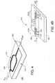
- Figs. 4A-B show an optical sensor 400 according to another embodiment of the present invention. More specifically, Fig. 4A shows a perspective three-dimensional view of sensor 400, and Fig. 4B shows an enlarged view of an optical resonator 416 of that sensor.
- Sensor 400 has a Mach-Zehnder interferometer (MZI) 410 formed on a substrate 402 and covered by an isolation layer 404 similar to MZI 110 of sensor 100 (Fig. 1).
- MZI 410 and MZI 110 is that the exposed arm of MZI 410 has two Bragg gratings 414a-b, which form resonator 416.
- Each grating 414 is formed with grooves 412 imprinted onto a waveguide 408 as shown in Fig. 4B.
- the reflectivity of each Bragg grating is appropriately chosen to couple light in and out of resonator 416 and to generate multiple round trips of the light within the resonator.
- a section of waveguide 408 between gratings 414a-b has a functional layer indicated in Fig. 4B by the Y-shaped symbols.
- grooves 412 do not have such a layer. This ensures that the resonator's optical properties are not substantially altered by the exposure to the analyte.
- Resonator 416 thus mostly serves to increase the effective interaction length of light within the exposed arm of MZI 410 with the bound analyte (schematically illustrated by diamonds in Fig. 4B). Due to the increased interaction length, the differential phase shift generated in MZI 410 is significantly greater than that in a similarly sized MZI 110 (Fig. 1). Therefore, the sensitivity of sensor 400 is advantageously improved compared to the sensitivity of sensor 100.
Landscapes
- Health & Medical Sciences (AREA)
- Life Sciences & Earth Sciences (AREA)
- Immunology (AREA)
- Engineering & Computer Science (AREA)
- Chemical & Material Sciences (AREA)
- Physics & Mathematics (AREA)
- Biomedical Technology (AREA)
- Hematology (AREA)
- Molecular Biology (AREA)
- Urology & Nephrology (AREA)
- Pathology (AREA)
- Analytical Chemistry (AREA)
- General Physics & Mathematics (AREA)
- General Health & Medical Sciences (AREA)
- Biochemistry (AREA)
- Cell Biology (AREA)
- Medicinal Chemistry (AREA)
- Food Science & Technology (AREA)
- Microbiology (AREA)
- Biotechnology (AREA)
- Chemical Kinetics & Catalysis (AREA)
- Plasma & Fusion (AREA)
- Tropical Medicine & Parasitology (AREA)
- Virology (AREA)
- Investigating Or Analysing Materials By Optical Means (AREA)
Abstract
Description
- The present invention relates to sensors and, more specifically, to optical devices for detecting chemical and biological substances.
- Substance analyzers are used in environmental monitoring, industrial process control, and medical, analytical, and military applications. For example, biological pathogens such as salmonella are often present in meat and poultry products. Since exposure to these pathogens is a health hazard, low concentrations, typically trace amounts, need to be detected quickly and reliably.
- In an analytical laboratory, specialized techniques such as mass spectrometry, chromatography, electro-chemical analysis, immunoassays, etc., are readily available to detect various chemical and biological substances (i.e., analytes) with great sensitivity and specificity. However, the available techniques are often time-consuming, labor-intensive, and/or relatively expensive. In addition, devices implementing these techniques are not adapted for portable use, nor are they adapted for use outside the laboratory.
- Problems in the prior art are addressed, in accordance with the principles of the present invention, by a portable waveguide sensor having one or more gratings adapted to cause a change in the optical characteristics of the sensor in the presence of a particular substance of interest, e.g., a biological pathogen. In one embodiment, the sensor has a waveguide, wherein a plurality of grooves imprinted onto the waveguide form a Bragg grating. The surface of the grooves has a functional layer adapted to bind the pathogen. When the pathogen binds to the functional layer, the binding shifts the spectral reflection band corresponding to the Bragg grating such that a probe light previously reflected by the grating now passes through the grating, thereby indicating the presence of the pathogen. In another embodiment, the sensor has a Mach-Zehnder interferometer (MZI), one arm of which has a resonator formed by two Bragg gratings. The surface of the resonator between the gratings has a functional layer whereas the Bragg gratings themselves do not have such a layer. Due to multiple reflections within the resonator, light coupled into the MZI interacts with the bound pathogen over a relatively large effective propagation length, which results in a relatively large differential phase shift and therefore advantageously high sensitivity to the pathogen.
-
- Fig. 1 shows a perspective three-dimensional view of a prior-art optical sensor;
- Figs. 2A-B show an optical sensor according to one embodiment of the present invention;
- Fig. 3 shows an optical sensing system having an array of sensors similar to the sensor shown in Fig. 2 according to one embodiment of the present invention; and
- Figs. 4A-B show an optical sensor according to another embodiment of the present invention.
- Reference herein to "one embodiment" or "an embodiment" means that a particular feature, structure, or characteristic described in connection with the embodiment can be included in at least one embodiment of the invention. The appearances of the phrase "in one embodiment" in various places in the specification are not necessarily all referring to the same embodiment, nor are separate or alternative embodiments mutually exclusive of other embodiments.
- Fig. 1 shows a perspective three-dimensional view of a prior-art
optical sensor 100 disclosed in an article by B. J. Luff, et al., published in J. Lightwave Technology, 1998, Vol. 16, No. 4, p. 583, the teachings of which are incorporated herein by reference.Sensor 100 is a planar waveguide device having a Mach-Zehnder interferometer (MZI) 110 formed on aglass substrate 102. Anisolation layer 104 that covers MZI 110 has anopening 106, which exposes one arm of the MZI to the environment, while keeping the other arm protected from such exposure. Anoptical input beam 120 applied tosensor 100 is split into two beam portions as it propagates throughMZI 110, which beam portions then recombine at the output of the MZI to produce anoptical output beam 130. The intensity ofbeam 130 depends on the differential phase shift between the beam portions at the recombination point. For example, when the differential phase shift is about 2πk, where k is an integer, the beam portions interfere constructively, which causesbeam 130 to have a relatively high intensity. On the other hand, when the differential phase shift is about (2k+1)π, the beam portions interfere destructively, which causesbeam 130 to have a relatively low intensity. - To enable detection of a chemical or biological substance of interest, hereafter termed the "analyte," the surface of the exposed MZI arm within
opening 106 is modified with a functional layer, which facilitates adsorption of the analyte onto the surface. Subsequently, whensensor 100 is exposed to the analyte, the analyte binds to the functional layer, thereby changing the arm's waveguide properties. This change alters the differential phase shift and, as a result, produces a corresponding intensity change ofbeam 130, which, upon detection, can be related to the presence of the analyte in the environment. However, one problem withsensor 100 is that its sensitivity may be relatively low. This is mostly due to the fact that light coupled into the exposed arm interacts with the adsorbed analyte by way of the evanescent field. Since the evanescent field is relatively weak, a relatively large interaction length is required to produce a detectable intensity change, which results in disadvantageously large and/or impractical MZI structures. - Figs. 2A-B show an
optical sensor 200 according to one embodiment of the present invention. More specifically, Fig. 2A shows a perspective three-dimensional view ofsensor 200, and Fig. 2B is an enlarged view of a grooved portion of that sensor.Sensor 200 is a planar waveguide device having awaveguide 208 formed on asubstrate 202. Waveguide 208 has a plurality ofgrooves 212, which form an integrated Bragggrating 214. As known in the art, one property of a Bragg grating is that it can reflect light corresponding to a relatively narrow spectral band while transmitting all other light. For example, grating 214 can be fabricated to have a reflection band with a center wavelength of λ0 and a spectral width of Δλ, where the spectral width is the wavelength difference between the band points having one half of the reflectivity corresponding to the center wavelength. In one implementation, λ0 and Δλ are about 1550 nm and 0.1 nm, respectively, and the reflectivity at λ0 is about 100%. - To enable analyte detection, the surface of
grooves 212 is modified with a functional layer similar to that ofsensor 100. In Fig. 2A, the functional layer is schematically illustrated by the Y-shaped symbols connected togrooves 212. Whensensor 200 is exposed to the analyte (schematically illustrated by diamonds in Fig. 2A), the analyte binds to the functional layer, thereby changing optical properties of grating 214. For example, for a periodic groove structure having a period of A (see Fig. 2B), the center wavelength is given by the following equation:
where n eff is the effective index of refraction corresponding to grating 214. When the analyte binds to the functional layer, it changes n eff and therefore λ0. Suppose that anoptical input beam 220 coupled intowaveguide 208 has wavelength λ'0 corresponding to the center wavelength ofgrating 214 in the absence of the analyte. Then, anoptical output beam 230 will have a very low intensity due to the Bragg reflection. However, whensensor 200 is exposed to the analyte, the analyte binding changes n eff and shifts the center wavelength to λ"0. This shift reduces the grating reflectivity at λ'0, which causes the intensity ofbeam 230 to increase, thereby indicating the presence of the analyte in the environment. Advantageously, the sensitivity ofsensor 200 is improved compared to the sensitivity ofdevice 100. The improvement is mostly due to the corrugated profile of grating 214, which increases the interaction cross-section of the probe light with the bound analyte insensor 200 compared to that in the evanescent-field-limited structure ofsensor 100. - Fig. 3 shows an
optical sensing system 300 according to one embodiment of the present invention.System 300 has an arrayed waveguide grating (AWG) 340, whose output ports are coupled to asensor 352.Sensor 352 is an arrayed sensor having threesensors 350a-c, each of which is similar tosensor 200 of Fig. 2. However,sensors 350a-c differ from each other in that (1) each sensor has a different center wavelength (i.e., λa, λb, and λc, respectively) and (2) each sensor has a different functional layer adapted to bind a different analyte. Functionalization of surface layers to enable analyte-specific conjugation is well known in the bio-technological arts and is described, for example, in a book by G.T. Hermanson, "Bioconjugate Techniques," Academic Press, San Diego, 1996, the teachings of which are incorporated herein by reference. Therefore,system 300 is adapted to detect three different analytes. One skilled in the art will appreciate that a sensing system adapted to detect two or four or more different analytes may be similarly designed. In a preferred embodiment,AWG 340 andsensor 352 are implemented in an integrated waveguide circuit. - In operation, a multiplexed
optical input beam 320 having wavelengths λa, λb, and λc is applied toAWG 340. Each component is then routed to the appropriate output port and coupled into the corresponding waveguide 308, where it impinges upon Bragg grating 314. Light passed through the gratings is measured using an array of photodetectors (not shown) to sense the presence of the different analytes, e.g., as described above forsensor 200. - Figs. 4A-B show an
optical sensor 400 according to another embodiment of the present invention. More specifically, Fig. 4A shows a perspective three-dimensional view ofsensor 400, and Fig. 4B shows an enlarged view of anoptical resonator 416 of that sensor.Sensor 400 has a Mach-Zehnder interferometer (MZI) 410 formed on asubstrate 402 and covered by anisolation layer 404 similar toMZI 110 of sensor 100 (Fig. 1). However, one difference betweenMZI 410 andMZI 110 is that the exposed arm ofMZI 410 has twoBragg gratings 414a-b, which formresonator 416. Each grating 414 is formed withgrooves 412 imprinted onto awaveguide 408 as shown in Fig. 4B. The reflectivity of each Bragg grating is appropriately chosen to couple light in and out ofresonator 416 and to generate multiple round trips of the light within the resonator. - A section of
waveguide 408 betweengratings 414a-b has a functional layer indicated in Fig. 4B by the Y-shaped symbols. In a preferred implementation,grooves 412 do not have such a layer. This ensures that the resonator's optical properties are not substantially altered by the exposure to the analyte.Resonator 416 thus mostly serves to increase the effective interaction length of light within the exposed arm ofMZI 410 with the bound analyte (schematically illustrated by diamonds in Fig. 4B). Due to the increased interaction length, the differential phase shift generated inMZI 410 is significantly greater than that in a similarly sized MZI 110 (Fig. 1). Therefore, the sensitivity ofsensor 400 is advantageously improved compared to the sensitivity ofsensor 100. - While this invention has been described with reference to illustrative embodiments, this description is not intended to be construed in a limiting sense. Although Bragg gratings of the invention are described as being implemented with grooves imprinted onto a waveguide, other grating implementations known in the art may similarly be used. The gratings may have reflection bands that have different center wavelengths and/or different shapes. Waveguide resonators of the invention may be implemented using different light-reflecting structures as known in the art. Various modifications of the described embodiments, as well as other embodiments of the invention, which are apparent to persons skilled in the art to which the invention pertains are deemed to lie within the principle and scope of the invention as expressed in the following claims.
- Although the steps in the following method claims, if any, are recited in a particular sequence with corresponding labeling, unless the claim recitations otherwise imply a particular sequence for implementing some or all of those steps, those steps are not necessarily intended to be limited to being implemented in that particular sequence.
Claims (10)
- A device, comprising an optical waveguide having a first grating and a second grating, said first and second gratings forming an optical resonator, wherein:at least a portion of the waveguide has a functional layer adapted to bind an analyte; andwhen the analyte binds to the functional layer, the binding changes optical characteristics of the optical resonator, whereby enabling detection of the analyte.
- The device of claim 1, wherein the first and second gratings are adapted to couple light in and out of the optical resonator and to generate multiple round trips of the light within the resonator.
- The device of claims 1 or 2, further comprising a Mach-Zehnder interferometer, MZI, having two arms, wherein:one arm includes said optical waveguide; andthe binding changes a differential phase shift in the MZI.
- The device of any one of claims 1 to 3, wherein a section of the optical waveguide between the first and second gratings has the functional layer.
- The device of any one of claims 1 to 4, wherein each of the first and second gratings is a Bragg grating formed by grooves imprinted into said optical waveguide.
- A method for detecting an analyte, comprising:transmitting light through an optical waveguide having a first grating and a second grating, said first and second gratings forming an optical resonator; andmeasuring the transmitted light using a photo-detector, wherein:at least a portion of the waveguide has a functional layer adapted to bind an analyte; andwhen the analyte binds to the functional layer, the binding changes optical characteristics of the optical resonator, whereby enabling detection of the analyte.
- The method of claim 6, wherein the first and second gratings are adapted to couple light in and out of the optical resonator and to generate multiple round trips of the coupled light within the resonator.
- The method of claims 6 or 7, further comprising the steps of:transmitting the light through a Mach-Zehnder interferometer, MZI, having two arms, wherein:one arm includes said optical waveguide; andthe binding changes a differential phase shift in the MZI; and measuring the differential phase shift.
- The method of any one of claims 6 to 8, wherein a section of the optical waveguide between the first and second gratings has the functional layer.
- The method of any one of claims 6 to 9, wherein each of the first and second gratings is a Bragg grating formed by grooves imprinted into said optical waveguide.
Applications Claiming Priority (2)
| Application Number | Priority Date | Filing Date | Title |
|---|---|---|---|
| US10/743,253 US7212693B2 (en) | 2003-12-22 | 2003-12-22 | Optical substance analyzer |
| EP04257334A EP1548424A3 (en) | 2003-12-22 | 2004-11-25 | Optical substance analyzer |
Related Parent Applications (1)
| Application Number | Title | Priority Date | Filing Date |
|---|---|---|---|
| EP04257334A Division EP1548424A3 (en) | 2003-12-22 | 2004-11-25 | Optical substance analyzer |
Publications (2)
| Publication Number | Publication Date |
|---|---|
| EP1710564A2 true EP1710564A2 (en) | 2006-10-11 |
| EP1710564A3 EP1710564A3 (en) | 2006-12-20 |
Family
ID=34552824
Family Applications (2)
| Application Number | Title | Priority Date | Filing Date |
|---|---|---|---|
| EP06014503A Withdrawn EP1710564A3 (en) | 2003-12-22 | 2004-11-25 | Optical substance analyzer |
| EP04257334A Withdrawn EP1548424A3 (en) | 2003-12-22 | 2004-11-25 | Optical substance analyzer |
Family Applications After (1)
| Application Number | Title | Priority Date | Filing Date |
|---|---|---|---|
| EP04257334A Withdrawn EP1548424A3 (en) | 2003-12-22 | 2004-11-25 | Optical substance analyzer |
Country Status (4)
| Country | Link |
|---|---|
| US (1) | US7212693B2 (en) |
| EP (2) | EP1710564A3 (en) |
| JP (1) | JP2005181334A (en) |
| KR (1) | KR20050063699A (en) |
Cited By (4)
| Publication number | Priority date | Publication date | Assignee | Title |
|---|---|---|---|---|
| WO2010150118A1 (en) * | 2009-06-08 | 2010-12-29 | Ramot At Tel Aviv University Ltd. | Single-waveguide bio-sensor based on propagating modes in a grating waveguide |
| EP2450693A1 (en) * | 2010-11-08 | 2012-05-09 | Nederlandse Organisatie voor toegepast -natuurwetenschappelijk onderzoek TNO | An arrayed waveguide grating (AWG) |
| CN104024895A (en) * | 2011-11-15 | 2014-09-03 | 英派尔科技开发有限公司 | Integrated optical sensor |
| TWI557408B (en) * | 2015-06-04 | 2016-11-11 | 國立屏東科技大學 | Glass capillary structure and glass capillary processing method thereof |
Families Citing this family (30)
| Publication number | Priority date | Publication date | Assignee | Title |
|---|---|---|---|---|
| US7155076B2 (en) * | 2001-06-15 | 2006-12-26 | The Regents Of The University Of California | Target molecules detection by waveguiding in a photonic silicon membrane |
| WO2005107368A2 (en) * | 2004-05-11 | 2005-11-17 | Tel Aviv University Future Technology Development Ltd. | Planar-resonator based optical chemo- and biosensors |
| GB0415881D0 (en) * | 2004-07-15 | 2004-08-18 | Univ Southampton | Multiwavelength optical sensors |
| US7327908B1 (en) * | 2005-03-07 | 2008-02-05 | Lightsmyth Technologies Inc. | Integrated optical sensor incorporating sets of diffractive elements |
| US7505641B1 (en) * | 2005-08-17 | 2009-03-17 | Polychromix Corporation | Optical biosensor incorporating wavelength encoding of multiple unlabeled analytes |
| JP2009511896A (en) * | 2005-10-12 | 2009-03-19 | コーニンクレッカ フィリップス エレクトロニクス エヌ ヴィ | All-polymer optical waveguide sensor |
| DE102005056225B4 (en) * | 2005-11-25 | 2008-12-18 | Petter, Jürgen | Electro-optical sensor and method for determining physical properties of a target substance via its refractive index |
| EP2137514B1 (en) * | 2007-03-13 | 2018-06-20 | Creoptix AG | Integrated optical sensor |
| US8218151B2 (en) | 2009-03-12 | 2012-07-10 | Tel Aviv University Future Technology Development Ltd | Light-emitting intra-cavity interferometric sensors |
| US20110220774A1 (en) * | 2009-11-13 | 2011-09-15 | Z-Image, Llc | Light Beam Detector |
| US8786852B2 (en) | 2009-12-02 | 2014-07-22 | Lawrence Livermore National Security, Llc | Nanoscale array structures suitable for surface enhanced raman scattering and methods related thereto |
| WO2012058716A1 (en) * | 2010-11-02 | 2012-05-10 | Edith Cowan University | An optical sensor for measuring a property of a fluid |
| SG188759A1 (en) * | 2011-09-21 | 2013-04-30 | Agency Science Tech & Res | Optical circuit for sensing a biological entity in a fluid and method of configuring the same |
| US9395304B2 (en) | 2012-03-01 | 2016-07-19 | Lawrence Livermore National Security, Llc | Nanoscale structures on optical fiber for surface enhanced Raman scattering and methods related thereto |
| ES2697131T3 (en) * | 2012-12-20 | 2019-01-22 | Univ Gent | Integrated optical sensor circuit |
| EP2757374A1 (en) * | 2013-01-17 | 2014-07-23 | F. Hoffmann-La Roche AG | Method for preparing an outer surface of a planar waveguide to be capable of binding target samples along a plurality of predetermined lines and a planar waveguide |
| EP3008450A2 (en) * | 2013-06-12 | 2016-04-20 | CSEM Centre Suisse d'Electronique et de Microtechnique SA | Measurement method based on an optical waveguide sensor system |
| TW201508249A (en) * | 2013-06-12 | 2015-03-01 | Optics Balzers Ag | Integrated optical waveguide sensor system |
| JP6260950B2 (en) * | 2013-09-10 | 2018-01-17 | 国立大学法人静岡大学 | Refractive index measurement method |
| EP3321663B1 (en) * | 2015-07-07 | 2021-03-24 | Furuno Electric Co., Ltd. | Measuring chip, measurement device, and measurement method |
| TWI687687B (en) * | 2019-01-11 | 2020-03-11 | 國立中正大學 | Dual grating sensor, detecting method and its manufacturing method |
| FR3105827B1 (en) * | 2019-12-27 | 2024-07-19 | Commissariat Energie Atomique | Photoacoustic or photothermal detector comprising an optical transducer |
| DE102020123800A1 (en) * | 2020-09-11 | 2022-03-17 | Fraunhofer-Gesellschaft zur Förderung der angewandten Forschung eingetragener Verein | Optical sensor, system and method for detecting pathogenic germs |
| EP4214490A4 (en) * | 2020-09-18 | 2024-10-09 | Salvus, LLC | INTERFERENCE METHOD OF DETECTION AND QUANTIFICATION SYSTEM AND METHOD OF USE |
| US12613187B2 (en) | 2020-09-18 | 2026-04-28 | Salvus, Llc | Interferometric detection and quantification system and methods of use in chemical processing |
| US12399172B2 (en) | 2020-09-18 | 2025-08-26 | Salvus, Llc | Interferometric detection and quantification system and methods of use in healthcare |
| US11747276B2 (en) | 2020-09-18 | 2023-09-05 | Salvus, Llc | Interferometric detection and quantification system and methods of use in agriculture |
| US11994504B2 (en) | 2020-09-18 | 2024-05-28 | Salvus, Llc | Interferometric detection and quantification system and methods of use in food processing and food supply chain |
| US11740177B2 (en) | 2020-09-18 | 2023-08-29 | Salvus, Llc | Interferometric detection and quantification system and methods of use in aquatics |
| CN113253403B (en) | 2021-06-17 | 2021-10-29 | 苏州浪潮智能科技有限公司 | An optical device, electronic device and programmable photonic integrated circuit |
Family Cites Families (9)
| Publication number | Priority date | Publication date | Assignee | Title |
|---|---|---|---|---|
| JPH0627703B2 (en) | 1985-05-29 | 1994-04-13 | アーティフィシャル センシング インスツルメンツ エイエスアイ アクチェンゲゼルシャフト | Optical sensor for selective detection of substance and detection of change in refractive index in measurement substance |
| WO1992019976A1 (en) * | 1991-04-26 | 1992-11-12 | Gesellschaft Zur Förderung Der Industrieorientierten Forschung An Den Schweizerischen Hochschulen Und Weiteren Institutionen | Process and device for determining measured quantities by means of an integrated optical sensor module |
| US5864641A (en) | 1997-04-11 | 1999-01-26 | F&S, Inc. | Optical fiber long period sensor having a reactive coating |
| GB0000896D0 (en) * | 2000-01-14 | 2000-03-08 | Univ Glasgow | Improved analytical chip |
| US6603560B1 (en) * | 2000-03-15 | 2003-08-05 | The Regents Of The University Of Michigan | High sensitivity fiber optic interferometric MEMS |
| JP2003531372A (en) * | 2000-04-14 | 2003-10-21 | ツェプトゼンス アクチエンゲゼルシャフト | Grating waveguide structure and its use for enhancing the excitation field |
| US6899849B2 (en) * | 2000-07-28 | 2005-05-31 | The Regents Of The University Of California | Integrated sensor |
| FR2830618B1 (en) * | 2001-10-05 | 2004-07-02 | Tijani Gharbi | OPTICAL SENSOR FOR DETECTION OF AT LEAST ONE CHEMICAL SUBSTANCE AND OPTICAL PROBES COMPRISING SUCH OPTICAL SENSORS |
| US6903815B2 (en) * | 2001-11-22 | 2005-06-07 | Kabushiki Kaisha Toshiba | Optical waveguide sensor, device, system and method for glucose measurement |
-
2003
- 2003-12-22 US US10/743,253 patent/US7212693B2/en not_active Expired - Lifetime
-
2004
- 2004-11-25 EP EP06014503A patent/EP1710564A3/en not_active Withdrawn
- 2004-11-25 EP EP04257334A patent/EP1548424A3/en not_active Withdrawn
- 2004-12-21 JP JP2004368616A patent/JP2005181334A/en active Pending
- 2004-12-21 KR KR1020040109109A patent/KR20050063699A/en not_active Withdrawn
Cited By (6)
| Publication number | Priority date | Publication date | Assignee | Title |
|---|---|---|---|---|
| WO2010150118A1 (en) * | 2009-06-08 | 2010-12-29 | Ramot At Tel Aviv University Ltd. | Single-waveguide bio-sensor based on propagating modes in a grating waveguide |
| EP2450693A1 (en) * | 2010-11-08 | 2012-05-09 | Nederlandse Organisatie voor toegepast -natuurwetenschappelijk onderzoek TNO | An arrayed waveguide grating (AWG) |
| WO2012064188A1 (en) * | 2010-11-08 | 2012-05-18 | Nederlandse Organisatie Voor Toegepast-Natuurwetenschappelijk Onderzoek Tno | An arrayed waveguide grating for detecting a change in an effective refracrive index |
| CN104024895A (en) * | 2011-11-15 | 2014-09-03 | 英派尔科技开发有限公司 | Integrated optical sensor |
| US8958071B2 (en) | 2011-11-15 | 2015-02-17 | Empire Technology Development Llc | Integrated optical sensor |
| TWI557408B (en) * | 2015-06-04 | 2016-11-11 | 國立屏東科技大學 | Glass capillary structure and glass capillary processing method thereof |
Also Published As
| Publication number | Publication date |
|---|---|
| KR20050063699A (en) | 2005-06-28 |
| US20050135723A1 (en) | 2005-06-23 |
| EP1548424A2 (en) | 2005-06-29 |
| US7212693B2 (en) | 2007-05-01 |
| EP1548424A3 (en) | 2005-10-19 |
| EP1710564A3 (en) | 2006-12-20 |
| JP2005181334A (en) | 2005-07-07 |
Similar Documents
| Publication | Publication Date | Title |
|---|---|---|
| US7212693B2 (en) | Optical substance analyzer | |
| US5663790A (en) | Method and apparatus for determination of refractive index | |
| EP1066507B1 (en) | Detection of a substance by refractive index change | |
| EP1182445B1 (en) | Integrated optic interferometric sensor | |
| US8823947B2 (en) | Optical sensor and method for detecting molecules | |
| CA2573097C (en) | Multiwavelength optical sensors | |
| US20100165351A1 (en) | Silicon photonic waveguide biosensor configurations | |
| WO2010030251A2 (en) | Integrated optical sensors operating in the frequency domain | |
| Katiyi et al. | Si nanostrip optical waveguide for on-chip broadband molecular overtone spectroscopy in near-infrared | |
| US20080267555A1 (en) | Plasmon-Polariton Refractive-Index Fiber Bio-Sensor with Fiber Bragg Grating | |
| Martens et al. | Comparison between Vernier-cascade and MZI as transducer for biosensing with on-chip spectral filter | |
| WO2013053930A1 (en) | Resonant biosensor | |
| US5644125A (en) | Spectrometer employing a Mach Zehnder interferometer created by etching a waveguide on a substrate | |
| EP2762858B1 (en) | Integrated interferometric optical sensor circuit | |
| US9068950B2 (en) | Vernier photonic sensor data-analysis | |
| JP7658623B2 (en) | Optical sensor chip and optical sensing system | |
| EP4660612A1 (en) | Plasmonic radiation biosensor | |
| EP1483547B1 (en) | Optical interferometer | |
| Boiarski et al. | Integrated optic biosensor for environmental monitoring | |
| EP4636389A1 (en) | Integrated photonic biosensor with layer discrimination ability and coherent reading system, and device, assembly and methods associated with same | |
| Rajasekar et al. | Photonic crystal-based sensors for biosensing applications | |
| la Grasta et al. | High-Sensitivity Biosensing with Silicon Photonic Ring Resonators | |
| Queirós et al. | Evanescent wave DNA-aptamer biosensor based on long period gratings for the specific recognition of E. coli | |
| Amartur et al. | Optical Chemical Sensors | |
| Hradetzky et al. | Interferometric sensor platform for biomolecular interaction analysis |
Legal Events
| Date | Code | Title | Description |
|---|---|---|---|
| PUAI | Public reference made under article 153(3) epc to a published international application that has entered the european phase |
Free format text: ORIGINAL CODE: 0009012 |
|
| 17P | Request for examination filed |
Effective date: 20060724 |
|
| AC | Divisional application: reference to earlier application |
Ref document number: 1548424 Country of ref document: EP Kind code of ref document: P |
|
| AK | Designated contracting states |
Kind code of ref document: A2 Designated state(s): AT BE BG CH CY CZ DE DK EE ES FI FR GB GR HU IE IS IT LI LU MC NL PL PT RO SE SI SK TR |
|
| AX | Request for extension of the european patent |
Extension state: AL HR LT LV MK YU |
|
| PUAL | Search report despatched |
Free format text: ORIGINAL CODE: 0009013 |
|
| AK | Designated contracting states |
Kind code of ref document: A3 Designated state(s): AT BE BG CH CY CZ DE DK EE ES FI FR GB GR HU IE IS IT LI LU MC NL PL PT RO SE SI SK TR |
|
| AX | Request for extension of the european patent |
Extension state: AL HR LT LV MK YU |
|
| 17Q | First examination report despatched |
Effective date: 20070316 |
|
| AKX | Designation fees paid |
Designated state(s): DE FR GB |
|
| STAA | Information on the status of an ep patent application or granted ep patent |
Free format text: STATUS: THE APPLICATION IS DEEMED TO BE WITHDRAWN |
|
| 18D | Application deemed to be withdrawn |
Effective date: 20070727 |