EP1708288A2 - Piezoelectric element, liquid-jet head using piezoelectric element and liquid-jet apparatus - Google Patents
Piezoelectric element, liquid-jet head using piezoelectric element and liquid-jet apparatus Download PDFInfo
- Publication number
- EP1708288A2 EP1708288A2 EP06006721A EP06006721A EP1708288A2 EP 1708288 A2 EP1708288 A2 EP 1708288A2 EP 06006721 A EP06006721 A EP 06006721A EP 06006721 A EP06006721 A EP 06006721A EP 1708288 A2 EP1708288 A2 EP 1708288A2
- Authority
- EP
- European Patent Office
- Prior art keywords
- piezoelectric
- piezoelectric layer
- piezoelectric element
- liquid
- layer
- Prior art date
- Legal status (The legal status is an assumption and is not a legal conclusion. Google has not performed a legal analysis and makes no representation as to the accuracy of the status listed.)
- Withdrawn
Links
Images




Classifications
-
- F—MECHANICAL ENGINEERING; LIGHTING; HEATING; WEAPONS; BLASTING
- F21—LIGHTING
- F21L—LIGHTING DEVICES OR SYSTEMS THEREOF, BEING PORTABLE OR SPECIALLY ADAPTED FOR TRANSPORTATION
- F21L13/00—Electric lighting devices with built-in electric generators
-
- B—PERFORMING OPERATIONS; TRANSPORTING
- B41—PRINTING; LINING MACHINES; TYPEWRITERS; STAMPS
- B41J—TYPEWRITERS; SELECTIVE PRINTING MECHANISMS, i.e. MECHANISMS PRINTING OTHERWISE THAN FROM A FORME; CORRECTION OF TYPOGRAPHICAL ERRORS
- B41J2/00—Typewriters or selective printing mechanisms characterised by the printing or marking process for which they are designed
- B41J2/005—Typewriters or selective printing mechanisms characterised by the printing or marking process for which they are designed characterised by bringing liquid or particles selectively into contact with a printing material
- B41J2/01—Ink jet
- B41J2/135—Nozzles
- B41J2/16—Production of nozzles
- B41J2/1621—Manufacturing processes
- B41J2/164—Manufacturing processes thin film formation
- B41J2/1646—Manufacturing processes thin film formation thin film formation by sputtering
-
- B—PERFORMING OPERATIONS; TRANSPORTING
- B41—PRINTING; LINING MACHINES; TYPEWRITERS; STAMPS
- B41J—TYPEWRITERS; SELECTIVE PRINTING MECHANISMS, i.e. MECHANISMS PRINTING OTHERWISE THAN FROM A FORME; CORRECTION OF TYPOGRAPHICAL ERRORS
- B41J2/00—Typewriters or selective printing mechanisms characterised by the printing or marking process for which they are designed
- B41J2/005—Typewriters or selective printing mechanisms characterised by the printing or marking process for which they are designed characterised by bringing liquid or particles selectively into contact with a printing material
- B41J2/01—Ink jet
- B41J2/135—Nozzles
- B41J2/14—Structure thereof only for on-demand ink jet heads
- B41J2/14201—Structure of print heads with piezoelectric elements
- B41J2/14233—Structure of print heads with piezoelectric elements of film type, deformed by bending and disposed on a diaphragm
-
- B—PERFORMING OPERATIONS; TRANSPORTING
- B41—PRINTING; LINING MACHINES; TYPEWRITERS; STAMPS
- B41J—TYPEWRITERS; SELECTIVE PRINTING MECHANISMS, i.e. MECHANISMS PRINTING OTHERWISE THAN FROM A FORME; CORRECTION OF TYPOGRAPHICAL ERRORS
- B41J2/00—Typewriters or selective printing mechanisms characterised by the printing or marking process for which they are designed
- B41J2/005—Typewriters or selective printing mechanisms characterised by the printing or marking process for which they are designed characterised by bringing liquid or particles selectively into contact with a printing material
- B41J2/01—Ink jet
- B41J2/135—Nozzles
- B41J2/16—Production of nozzles
- B41J2/1607—Production of print heads with piezoelectric elements
- B41J2/161—Production of print heads with piezoelectric elements of film type, deformed by bending and disposed on a diaphragm
-
- B—PERFORMING OPERATIONS; TRANSPORTING
- B41—PRINTING; LINING MACHINES; TYPEWRITERS; STAMPS
- B41J—TYPEWRITERS; SELECTIVE PRINTING MECHANISMS, i.e. MECHANISMS PRINTING OTHERWISE THAN FROM A FORME; CORRECTION OF TYPOGRAPHICAL ERRORS
- B41J2/00—Typewriters or selective printing mechanisms characterised by the printing or marking process for which they are designed
- B41J2/005—Typewriters or selective printing mechanisms characterised by the printing or marking process for which they are designed characterised by bringing liquid or particles selectively into contact with a printing material
- B41J2/01—Ink jet
- B41J2/135—Nozzles
- B41J2/16—Production of nozzles
- B41J2/1621—Manufacturing processes
- B41J2/1623—Manufacturing processes bonding and adhesion
-
- B—PERFORMING OPERATIONS; TRANSPORTING
- B41—PRINTING; LINING MACHINES; TYPEWRITERS; STAMPS
- B41J—TYPEWRITERS; SELECTIVE PRINTING MECHANISMS, i.e. MECHANISMS PRINTING OTHERWISE THAN FROM A FORME; CORRECTION OF TYPOGRAPHICAL ERRORS
- B41J2/00—Typewriters or selective printing mechanisms characterised by the printing or marking process for which they are designed
- B41J2/005—Typewriters or selective printing mechanisms characterised by the printing or marking process for which they are designed characterised by bringing liquid or particles selectively into contact with a printing material
- B41J2/01—Ink jet
- B41J2/135—Nozzles
- B41J2/16—Production of nozzles
- B41J2/1621—Manufacturing processes
- B41J2/1626—Manufacturing processes etching
- B41J2/1629—Manufacturing processes etching wet etching
-
- B—PERFORMING OPERATIONS; TRANSPORTING
- B41—PRINTING; LINING MACHINES; TYPEWRITERS; STAMPS
- B41J—TYPEWRITERS; SELECTIVE PRINTING MECHANISMS, i.e. MECHANISMS PRINTING OTHERWISE THAN FROM A FORME; CORRECTION OF TYPOGRAPHICAL ERRORS
- B41J2/00—Typewriters or selective printing mechanisms characterised by the printing or marking process for which they are designed
- B41J2/005—Typewriters or selective printing mechanisms characterised by the printing or marking process for which they are designed characterised by bringing liquid or particles selectively into contact with a printing material
- B41J2/01—Ink jet
- B41J2/135—Nozzles
- B41J2/16—Production of nozzles
- B41J2/1621—Manufacturing processes
- B41J2/1632—Manufacturing processes machining
-
- B—PERFORMING OPERATIONS; TRANSPORTING
- B41—PRINTING; LINING MACHINES; TYPEWRITERS; STAMPS
- B41J—TYPEWRITERS; SELECTIVE PRINTING MECHANISMS, i.e. MECHANISMS PRINTING OTHERWISE THAN FROM A FORME; CORRECTION OF TYPOGRAPHICAL ERRORS
- B41J2/00—Typewriters or selective printing mechanisms characterised by the printing or marking process for which they are designed
- B41J2/005—Typewriters or selective printing mechanisms characterised by the printing or marking process for which they are designed characterised by bringing liquid or particles selectively into contact with a printing material
- B41J2/01—Ink jet
- B41J2/135—Nozzles
- B41J2/16—Production of nozzles
- B41J2/1621—Manufacturing processes
- B41J2/164—Manufacturing processes thin film formation
- B41J2/1642—Manufacturing processes thin film formation thin film formation by CVD [chemical vapor deposition]
-
- F—MECHANICAL ENGINEERING; LIGHTING; HEATING; WEAPONS; BLASTING
- F21—LIGHTING
- F21L—LIGHTING DEVICES OR SYSTEMS THEREOF, BEING PORTABLE OR SPECIALLY ADAPTED FOR TRANSPORTATION
- F21L4/00—Electric lighting devices with self-contained electric batteries or cells
- F21L4/08—Electric lighting devices with self-contained electric batteries or cells characterised by means for in situ recharging of the batteries or cells
-
- H—ELECTRICITY
- H10—SEMICONDUCTOR DEVICES; ELECTRIC SOLID-STATE DEVICES NOT OTHERWISE PROVIDED FOR
- H10N—ELECTRIC SOLID-STATE DEVICES NOT OTHERWISE PROVIDED FOR
- H10N30/00—Piezoelectric or electrostrictive devices
- H10N30/20—Piezoelectric or electrostrictive devices with electrical input and mechanical output, e.g. functioning as actuators or vibrators
- H10N30/204—Piezoelectric or electrostrictive devices with electrical input and mechanical output, e.g. functioning as actuators or vibrators using bending displacement, e.g. unimorph, bimorph or multimorph cantilever or membrane benders
- H10N30/2047—Membrane type
-
- H—ELECTRICITY
- H10—SEMICONDUCTOR DEVICES; ELECTRIC SOLID-STATE DEVICES NOT OTHERWISE PROVIDED FOR
- H10N—ELECTRIC SOLID-STATE DEVICES NOT OTHERWISE PROVIDED FOR
- H10N30/00—Piezoelectric or electrostrictive devices
- H10N30/80—Constructional details
- H10N30/85—Piezoelectric or electrostrictive active materials
- H10N30/853—Ceramic compositions
- H10N30/8548—Lead-based oxides
- H10N30/8554—Lead-zirconium titanate [PZT] based
-
- B—PERFORMING OPERATIONS; TRANSPORTING
- B41—PRINTING; LINING MACHINES; TYPEWRITERS; STAMPS
- B41J—TYPEWRITERS; SELECTIVE PRINTING MECHANISMS, i.e. MECHANISMS PRINTING OTHERWISE THAN FROM A FORME; CORRECTION OF TYPOGRAPHICAL ERRORS
- B41J2/00—Typewriters or selective printing mechanisms characterised by the printing or marking process for which they are designed
- B41J2/005—Typewriters or selective printing mechanisms characterised by the printing or marking process for which they are designed characterised by bringing liquid or particles selectively into contact with a printing material
- B41J2/01—Ink jet
- B41J2/135—Nozzles
- B41J2/14—Structure thereof only for on-demand ink jet heads
- B41J2/14201—Structure of print heads with piezoelectric elements
- B41J2/14233—Structure of print heads with piezoelectric elements of film type, deformed by bending and disposed on a diaphragm
- B41J2002/14241—Structure of print heads with piezoelectric elements of film type, deformed by bending and disposed on a diaphragm having a cover around the piezoelectric thin film element
-
- B—PERFORMING OPERATIONS; TRANSPORTING
- B41—PRINTING; LINING MACHINES; TYPEWRITERS; STAMPS
- B41J—TYPEWRITERS; SELECTIVE PRINTING MECHANISMS, i.e. MECHANISMS PRINTING OTHERWISE THAN FROM A FORME; CORRECTION OF TYPOGRAPHICAL ERRORS
- B41J2/00—Typewriters or selective printing mechanisms characterised by the printing or marking process for which they are designed
- B41J2/005—Typewriters or selective printing mechanisms characterised by the printing or marking process for which they are designed characterised by bringing liquid or particles selectively into contact with a printing material
- B41J2/01—Ink jet
- B41J2/135—Nozzles
- B41J2/14—Structure thereof only for on-demand ink jet heads
- B41J2002/14419—Manifold
-
- B—PERFORMING OPERATIONS; TRANSPORTING
- B41—PRINTING; LINING MACHINES; TYPEWRITERS; STAMPS
- B41J—TYPEWRITERS; SELECTIVE PRINTING MECHANISMS, i.e. MECHANISMS PRINTING OTHERWISE THAN FROM A FORME; CORRECTION OF TYPOGRAPHICAL ERRORS
- B41J2202/00—Embodiments of or processes related to ink-jet or thermal heads
- B41J2202/01—Embodiments of or processes related to ink-jet heads
- B41J2202/03—Specific materials used
Definitions
- the present invention relates to a piezoelectric element including a piezoelectric layer formed of a piezoelectric material, and a liquid-jet head using the piezoelectric element as well as a liquid-jet apparatus.
- a piezoelectric element is configured in a manner that a piezoelectric layer is interposed between two electrodes.
- the piezoelectric layer is made of, for example, a piezoelectric material showing an electrical mechanical conversion function.
- the piezoelectric layer is configured of, for example, crystallized piezoelectric ceramics.
- inkjet recording head with the following configuration, as a liquid-head jet using such a piezoelectric element.
- a part of pressure generating chambers communicating with nozzle orifices from which ink droplets are ejected is constructed with a vibration plate.
- the vibration plate is deformed by piezoelectric elements, and thus ink in each of the pressure generating chambers is pressurized. Accordingly, ink droplets are ejected from each of the nozzle orifices.
- Two types of inkjet recording heads have been put into practical use.
- One of the two types uses a piezoelectric actuator of a longitudinal vibration mode in which the piezoelectric actuator expands and contracts in a longitudinal direction of piezoelectric elements.
- the other type uses a piezoelectric actuator of a flexure vibration mode.
- an inkjet recording head formed in the following manner has been known.
- An even piezoelectric layer is formed on the entire surface of a vibration plate by use of a film-forming technique. Then, this piezoelectric layer is cut into shapes corresponding to the pressure generating chambers by a lithography method. Thereby, the piezoelectric elements are formed respectively in the pressure generating chambers in a manner that the piezoelectric can be independent from one anther.
- piezoelectric layer piezoelectric film
- PZT lead zirconate titanate
- various characteristics, such as displacement characteristics and durability, of the piezoelectric element including such a piezoelectric layer are largely dependent on crystallinity of the piezoelectric layer.
- a relative permittivity, a coercive electric field and the like are regulated.
- it cannot be said that such a piezoelectric element disclosed in Japanese Patent Laid-Open Official Gazette No. 2001-284671 has sufficient crystallinity.
- an object of the present invention is to provide a piezoelectric element in which crystallinity of a piezoelectric layer is improved, and which has uniform characteristics of the piezoelectric layer, a liquid-jet head using a piezoelectric element as well as a liquid-jet apparatus.
- a first aspect of the present invention for the purpose of solving the aforementioned problems is a piezoelectric element characterized by including: a lower electrode provided to one surface side of a substrate; a piezoelectric layer which is made of a piezoelectric material containing lead (Pb), zirconium (Zr) and titanium (Ti), and which is provided above the lower electrode; and an upper electrode provided above the piezoelectric layer.
- the piezoelectric layer is characterized in that a relative permittivity of the piezoelectric layer is 750 to 1500, and a coercive electric field of the piezoelectric layer is 10 to 40kV/cm.
- crystallinity of the piezoelectric layer is significantly improved. Accordingly, it is possible to provide a piezoelectric element which is excellent in displacement characteristics, and which has a high withstand voltage and a longer durability life.
- a second aspect of the present invention is the piezoelectric element according to the first aspect, which is characterized in that the coercive electric field of the piezoelectric layer is 20 to 30kV/cm and a residual polarization intensity of the piezoelectric layer is 10 to 15 ⁇ C/cm 2 .
- the crystallinity of the piezoelectric layer achieves greater excellence, and the displacement characteristics and durablity life of the piezoelectric layer are further improved.
- a third aspect of the present invention is the piezoelectric element according to the first aspect, which is characterized in that the film thickness of the piezoelectric layer is 0.5 to 5 ⁇ m.
- the crystallinity of the piezoelectric layer is improved significantly without fault.
- the composition ratio of the piezoelectric layer by adjusting the composition ratio of the piezoelectric layer to be within a predetermined range, it is possible to improve the crystallinity of the piezoelectric layer further.
- a fifth aspect of the present invention is a piezoelectric element according to first aspect, which is characterized in that the piezoelectric material is lead zirconate titanate.
- the piezoelectric element which is excellent in displacement characteristics and durability.
- a sixth aspect of the present invention is a liquid-jet head characterized by including: the piezoelectric element according to of the first aspect; and a passage-forming substrate, in which the piezoelectric element is provided to one surface side of the passage-forming substrate, and to which a pressure generating chamber communicating with a nozzle orifice is provided.
- a seventh aspect of the present invention is a liquid-jet head characterized by including the liquid-jet head according to the sixth aspect.
- Fig. 1 is an exploded perspective view showing a schematic configuration of an inkjet recording head according to a first embodiment of the present invention.
- Fig. 2A is a plan view of the inkjet recording head shown in Fig. 1
- Fig. 2B is a cross-sectional view of the inkjet recording head taken along the A-A' line of Fig. 2A.
- a passage-forming substrate 10 is formed of a single crystal silicon substrate in which crystals are oriented to the (110) plane direction.
- An elastic film 50 is formed on one of the two surfaces of the passage-forming substrate 10, as illustrated.
- the elastic film 50 has a thickness of 0.5 to 2 ⁇ m, and is made of silicon dioxide beforehand formed by thermal oxidation.
- a plurality of pressure generating chambers 12 compartmentalized by compartment walls 11 are arranged side-by-side in the width direction of the pressure generating chambers 12.
- a communicating portion 13 is formed, the pressure generating chambers 12 being of the passage-forming substrate 10.
- the communicating portion 13 communicates with each of the pressure generating chambers 12 through each of ink supply paths 14 respectively provided to the pressure generating chambers 12.
- the communicating portion 13 constitutes a part of a reservoir which will be a common ink chamber for each of the pressure generation chambers 12 while communicating with a reservoir portion of a protection substrate which will be described later.
- Each of the ink supply paths 14 is formed with a width narrower than that of the pressure generating chamber 12, and thus keeps constant the passage resistance of ink flowing from the communicating portion 13 to the pressure generating chamber 12.
- a nozzle plate 20 is fixed to an aperture surface of the passage-forming substrate 10 with a mask film 52 interposed in between by use of an adhesive agent, a thermal adhesive film or the like.
- the mask film 52 will be described later.
- nozzle orifices 21 are drilled.
- the nozzle orifices 21 communicate respectively with the pressure-generating chambers 12 at vicinity of ends of the pressure-generating chambers 12, which ends are opposite the ink supply paths 14.
- the nozzle plate 20 is formed of, for example, glass ceramics, single crystal silicon substrate, stainless steel or the like.
- the elastic film 50 is formed on the other surface of the passage-forming substrate 10 which is the side opposite the aperture surface.
- the elastic film 50 has a thickness of, for example, approximately 1.0 ⁇ m, and is made of silicon dioxide.
- An insulation film 55 is formed on this elastic film 50 by laminating the insulation film 55 over this elastic film 50.
- the insulation film 55 has a thickness of approximately 0.4 ⁇ m, and is made of zirconia (Zr0 2 ) and the like.
- piezoelectric elements 300 are formed on this insulation film 55.
- Each of the piezoelectric elements 300 is configured of a lower electrode film 60, a piezoelectric layer 70 and an upper electrode film 80.
- the lower electrode film 60, the piezoelectric layer 70 and the upper electrode 80 have thicknesses of, for example, approximately 0.1 to 0.2 ⁇ m, approximately 0.5 to 5 ⁇ m and approximately 0.05 ⁇ m respectively.
- the piezoelectric element 300 is configured in the following manner.
- One of the two electrodes of the piezoelectric element 300 is used as a common electrode.
- the other electrode and the piezoelectric layer 70 are patterned in each of the pressure generating chambers 12.
- a piezoelectric strain occurs due to application of a voltage to the two electrodes.
- This portion is called a "piezoelectric active portion".
- the lower electrode film 60 is used as a common electrode for the piezoelectric elements 300
- the upper electrode films 80 are used as individual electrodes of the piezoelectric elements 300.
- the piezoelectric active portions are formed respectively the pressure generating chambers 12.
- a lead electrode 90 is connected to each of the upper electrode films 80 of such piezoelectric elements 300.
- the lead electrode 90 is made of, for example, gold (Au) and the like. A voltage is selectively applied to each of the piezoelectric elements 300 through the lead electrode 90.
- each of the lower electrode film 60 and the upper electrode film 80, which constitute the piezoelectric element 300 are made of metallic materials each having a relatively high electrical permittivity.
- the metallic materials are, for example, platinum (Pt), iridium (Ir) and the like.
- the piezoelectric layer 70 is made of a piezoelectric material containing at least lead (Pb), zirconium (Zr) and titanium (Ti).
- PZT lead zirconate titanate
- the piezoelectric constant thereof reach a higher degree of excellence.
- the piezoelectric constant d 31 is 150 to 250 (pC/N). Accordingly, displacement characteristics of the piezoelectric element 300 improve.
- the piezoelectric layer 70 with such characteristics is excellent in crystallinity, characteristics thereof such as a withstand voltage are significantly improved. Accordingly, if the displacement characteristics of the piezoelectric element 300 are improved, the durability life thereof is significantly improved at the same time. Additionally, since there are almost no variations between characteristics of the piezoelectric layers 70 , which constitute the piezoelectric element 300, characteristics of ejecting ink droplets from the respective nozzle orifices 21 become uniform.
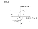
- the residual polarization intensity Pr is a value, for example, obtained by use of the 2Pr of the hysteresis loop of the piezoelectric layer as shown in Fig. 3.
- the piezoelectric layer 70 is formed of lead zirconate titanate (PZT) in this embodiment.
- PZT lead zirconate titanate
- a piezoelectric material configuring the piezoelectric layer 70 contains at least lead (Pb), zirconium (Zr) and titanium (Ti).
- Pb lead
- Zr zirconium
- Ti titanium
- a piezoelectric material obtained by adding metallic oxide such as niobium oxide, nickel oxide or magnesium oxide to lead zirconate titanate (PZT), or the like.
- a protection plate 30 is joined to the top of the passage-forming substrate 10 over which such piezoelectric elements 300 are formed.
- the protection plate 30 is joined to the top of the lower electrode film 60, the elastic film 50 and the lead electrodes 90 with an adhesive agent or the like.
- the protection plate 30 is provided with a piezoelectric element holding portion 31 having a cavity large enough for the piezoelectric elements 300 to move without hindrance.
- the piezoelectric element holding portion 31 is provided to a region which is opposite the piezoelectric elements 300. Note that it suffices if the piezoelectric element holding portion 31 has a cavity large enough for the piezoelectric elements 300 to move without hindrance. It does not matter whether or not the cavity is sealed up.
- the protection plate 30 is provided with a reservoir portion 32 in a region which is opposite the communicating portion 13. As described above, this reservoir portion 32 constitutes the reservoir 100 while communicating with the communicating portion 13 of the passage-forming substrate 10.
- the reservoir 100 functions as a common ink chamber for the pressure generating chambers 12.
- a through-hole 33 is provided to a region between the piezoelectric element holding portion 31 and reservoir portion 32 of the protection plate 30. The through-hole 33 penetrates through the protection plate 30 in the thickness direction. In the through-hole 33, a part of lower electrode film 60 and tip portions of the respective lead electrodes 90 are exposed. Although it is not illustrated, an end of a connection wire extended from a drive IC is connected to the lower electrode film 60 and each of the lead electrodes 90.
- the protection plate 30 is formed using a single crystal silicon substrate which is the same material as that for the passage-forming substrate 10.
- a compliance plate 40 configured of a sealing film 41 and a fixed plate 42 is joined to the top of the protection plate 30.
- the sealing film 41 is made of a flexible material with a lower rigidity (for example, a polyphenylen sulfide (PPS) film with a thickness of 6 ⁇ m).
- PPS polyphenylen sulfide
- One end of the reservoir portion 32 is sealed up by this sealing film 41.
- the fixed plate 42 is formed of a hard material such as a metal (for example, stainless steel (SUS) or the like with a thickness of 30 ⁇ m).
- a region of this fixed plate 42, which region is opposite the reservoir 100, is an opening portion 43 which is obtained by completely removing a portion corresponding to the region in the thickness direction. Accordingly, one end of the reservoir 100 is sealed up only by the sealing film 41 which is flexible.
- Such an inkjet recording head takes in ink from external ink supply means, which is not illustrated, and fills the interior ranging from the reservoir 100 through the nozzle orifices 21 with ink. Thereafter, the inkjet recording head applies a voltage between the lower electrode film 60 and each of the upper electrode films 80 corresponding to the pressure generating chambers 12, in accordance with recording signals from the drive circuit. Thus, the inkjet recording head deforms the elastic film 50, the lower electrode films 60 and the piezoelectric layers 70 with flexure. This deformation raises the pressure in each of the pressure generating chambers 12, and thereby ink droplets are ejected from the nozzle orifices 21.
- Figs. 4A to 7C are cross-sectional views of the pressure generating chamber 12 in the longitudinal direction.
- a silicon dioxide film 51 is formed in a following manner.
- An wafer for passage- forming substrate 110 is thermally oxidized in a diffusion furnace at approximately 1100°C.
- the silicon dioxide film 51 which will constitute the elastic film 50, is formed on the surface of the wafer for passage-forming substrate 110.
- silicon wafer which has a relatively large thickness as 625 ⁇ m and high rigidity is used as the wafer for passage-forming substrate 110.
- the insulation film 55 made of zirconia is formed on the elastic film 50 (the silicon dioxide film 51).
- a zirconium (Zr) layer is formed on the elastic film 50 (the silicon dioxide film 51) by means of , for example, a sputtering method or the like.
- the zirconium layer is thermally oxidized, for example, in a diffusion furnace at approximately 500 to 1200°C.
- the insulation film 55 made of zirconia (ZrO 2 ) is formed.
- the lower electrode film 60 formed of, for example, platinum (Pt), iridium (Ir) or the like is formed over the insulation film 55.
- the lower electrode film 60 is patterned in a predetermined shape.
- a seed titanium layer 65 having a predetermined thickness is formed over the lower electrode film 60 and the insulation film 55 by coating titanium (Ti) by use of, for example, a sputtering method or the like.
- the piezoelectric layer 70 is formed on the seed titanium layer 65.
- the piezoelectric layer 70 is made of lead zirconate titanate in this embodiment.
- the piezoelectric layer 70 is formed by use of what is termed as a sol-gel method in this embodiment. According to the sol-gel method, what is termed as sol is obtained by dissolving and dispersing a metal-organic substance in a catalytic. This sol is coated and dried to be turned into gel.
- the gel is sintered at a higher temperature.
- the piezoelectric layer 70 made of a metal-oxide substance is obtained.
- the method of manufacturing the piezoelectric layer 70 is not limited to the sol-gel method.
- the MOD (Metal-Organic Decomposition) method or the like may be used.
- a piezoelectric precursor film 71 which is a PZT precursor film is formed on the seed titanium layer 65.
- the sol (liquid solution) containing the metal-organic compound is coated to the top of the wafer for passage- forming substrate 110.
- the piezoelectric precursor film 71 is heated at a predetermined temperature, and thus is dried for a certain period.
- the piezoelectric precursor film 71 is dried by means of evaporating a solvent of sol.
- the piezoelectric precursor film 71 is degreased in an atmosphere for a predetermined period at a predetermined temperature.
- the degreasing which has been referred to in this respect, means that organic components of the film made from sol are eliminated therefrom, for example, as NO 2 , CO 2 H 2 O and the like.
- a piezoelectric film 72 is formed as shown in Fig. 5B in the following manner.
- the piezoelectric precursor films 71 each with a predetermined thickness are formed.
- the piezoelectric precursor films 71 undergo thermal processing in a diffusion furnace to be crystallized.
- the piezoelectric film 72 is formed.
- the piezoelectric precursor films 71 are sintered to cause crystals thereof to grow with the seed titanium layer 65 as a seed, whereby the piezoelectric film 72 is formed.
- a sintering temperature is preferably 650 to 850°C.
- the piezoelectric precursor films 71 are sintered for half an hour at 700°C to form the piezoelectric film 72. Note that crystals of the piezoelectric film 72 thus formed have preferred orientations of the (100) plane.
- the coating, drying, degreasing, and sintering steps are repeatedly carried out for a plurality of times to form the piezoelectric layer 70 having a certain thickness.
- the piezoelectric layer 70 is formed of, for example, five piezoelectric films 72 as shown in Fig. 5C. Note that in a case of forming the piezoelectric layer 70 by performing the sintering for a plurality of times, it is preferable that the total sintering (heating) time be not more than half an hour to three hours.
- the piezoelectric layer 70 in this manner, it is possible to stably form the piezoelectric layer 70 with preferable characteristics including a relative permittivity of 750 to 1500 and a coercive electric field Ec of 10 to 40kV/cm.
- the coercive electric field Ec and residual polarization intensity Pr of the piezoelectric layer 70 are approximately 20 to 30 (kV/cm) and approximately 10 to 15 ( ⁇ C/cm 2 ) respectively.
- the upper electrode film 80 is formed entirely on the top of the wafer for passage-forming substrate 110 as shown in Fig. 6A.
- the upper electrode film 80 is made of, for example, iridium.
- the piezoelectric element 300 is formed by patterning the piezoelectric layer 70 and the upper electrode film 80 in each of regions which are opposite the pressure generating chambers 12.
- Fig. 8 shows the results of measuring residual polarization intensity (2Pr) and coercive electric fields (2Ec) of the samples.
- the residual polarization intensity (2Pr) is 20 to 30 ( ⁇ C/cm 2 ) and the coercive electric field (2Ec) is 40 to 60 (kV/cm).
- such a piezoelectric layer 70 has a piezoelectric constant d 31 as high as 150 to 250 (pC/N) as described above, whereby the displacement characteristics of the piezoelectric element 300 are significantly improved.
- the piezoelectric layer 70 is also excellent in crystallinity, thus characteristics such as withstand voltage are also significantly improved, for example.
- a lead electrode 90 drawn out from each of the piezoelectric elements 300 is formed.
- the lead electrode 90 is formed as shown in Fig. 6C in the following manner.
- a metal layer 91 is formed the entire top surface of the wafer for passage-forming substrate 110.
- the metal layer 91 is made, for example, of gold (Au) and the like.
- the lead electrodes 90 are formed by patterning the metal layer 91 in each of the piezoelectric elements 300 by use of a mask pattern (not illustrated) made, for example, of a resist or the like.
- a wafer for protection plate 130 is joined to the top of the wafer for passage-forming substrate 110 on the side where piezoelectric elements 300 are formed.
- the wafer for passage-forming substrate 110 is silicon wafer and is to become plural protection plates 30.
- the wafer for protection plate 130 has a thickness of, for example, approximately 400 ⁇ m. Note that, accordingly, rigidity of the wafer for passage-forming substrate 110 is significantly increased by joining the wafer for protection plate 130 to the wafer for passage-forming substrate 110.
- the wafer for passage-forming substrate 110 is caused to have a predetermined thickness by means of polishing the wafer for passage-forming substrate 110 and then performing wet-etching with fluoro-nitric acid.
- the wafer for passage-forming substrate 110 undergoes etching processing in order that the wafer for passage-forming substrate 110 has a thickness of, for example, approximately 70 ⁇ m.
- a mask film 52 is newly formed on the bottom surface of the wafer for passage-forming substrate 110 and is patterned in a predetermined shape.
- the mask film 52 is made of, for example, silicon nitride (SiN).
- the piezoelectric layer is formed configuring the piezoelectric element and having a relative permittivity of 750 to 1500 and a coercive electric field of 10 to 40kV/cm.
- This increases the piezoelectric constant d 31 of the piezoelectric layer 70. Accordingly, the displacement characteristics of the piezoelectric element 300 improve.
- the crystallinity of the piezoelectric layer 70 improves, characteristics such as the withstand voltage are significantly improved, for example. Accordingly, the displacement characteristics of the piezoelectric element 300 are improved while the durability life thereof is also significantly extended.
- a sample of piezoelectric element prepared under the above-mentioned conditions was caused to undergo a durability test in which a predetermined drive pulse is continuously applied to the sample thirty billion times.
- Fig. 9 shows the result of examining the amount of displacement of the piezoelectric element and a decrease in the displacement.
- the drive pulse applied in the durability test was a sine wave with a voltage of 50V and a frequency of 100kHz.
- a drive pulse applied during displacement measurement was a trapezoidal wave with a voltage of 30V and a frequency of 800Hz.
- the displacement amount is decreased in accordance with the increase in the number of the withstand pulses.
- the rate of displacement decrease was increased.
- the rate of displacement decrease was kept to be a significantly low rate of 13.3%, even after the drive pulse is applied thirty billion times.
- the durability life of the piezoelectric element is significantly improved according to the present invention.
- the piezoelectric layer is formed by use of the sol-gel method.
- the piezoelectric layer may be formed by means of a sputtering method, the CVD method or the like.
- piezoelectric precursor films are sintered at 650 to 750°C.
- post-annealing is performed on the piezoelectric precursor films for half an hour to three hours.
- the lower films may be formed by means of the sputtering or CVD method and the upper films may be formed by means of the sol-gel method, the MOD method or the like.
- each of the inkjet recording heads constitutes a part of a recording head unit provided with an ink passage communicating with an ink cartridge and the like, and is installed in an inkjet recording apparatus.
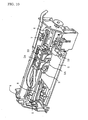
- Fig. 10 is a schematic configuration diagram showing an example of the inkjet recording apparatus.
- recording head units 1A and 1B each including the inkjet recording head are detachably provided to cartridges 2A and 2B constituting ink supply means.
- a carriage 3 on which the. recording head units 1A and 1B are mounted is provided to a carriage shaft 5 fixed to the device main body 4 in a way that the carriage 3 can be freely moved in the direction in which the shaft extends.
- These recording head units 1A and 1B are, for example, assigned to eject black ink compositions and color ink compositions respectively.
- a drive power from a drive motor 6 is transmitted to the carriage 3 though a plurality of gears, which are not illustrated, and a timing belt 7.
- the carriage 3 on which the recording head units 1A and 1B are mounted is caused to move along the carriage shaft 5.
- the device main body 4 is provided with a platen 8 along the carriage shaft 5.
- a recording sheet S which is a recording medium such as a sheet of paper, and which has been fed by feed rollers and the like, is designed to be transferred on the platen 8, the feed rollers being not illustrated.
- the present invention is intended to be widely applied to the entire range of liquid-jet heads, although the first embodiment has been described above giving the inkjet recording head as an example of liquid-jet heads. It goes without saying that the present invention can be applied to any liquid-jet head which ejects a liquid other than ink.
- liquid-jet head which eject a liquid other than ink includes various recording heads used for image recording devices such as printers; color-material-jet heads used for manufacturing color filters of liquid crystal display devices and the like; electrode-material-jet heads used for forming electrodes of organic EL display devices, FED (Field Emission Display) devices and the like; bio-organic-substance-jet heads used for manufacturing bio-chips; and the like.
- the present invention can be applied not only to piezoelectric elements used for liquid-jet heads but also to piezoelectric elements installed in other various devices such as microphones, sounding bodies, various vibrators, calling devices or the like.
Landscapes
- Engineering & Computer Science (AREA)
- Manufacturing & Machinery (AREA)
- General Engineering & Computer Science (AREA)
- Chemical & Material Sciences (AREA)
- Ceramic Engineering (AREA)
- Life Sciences & Earth Sciences (AREA)
- Sustainable Development (AREA)
- Sustainable Energy (AREA)
- Particle Formation And Scattering Control In Inkjet Printers (AREA)
- General Electrical Machinery Utilizing Piezoelectricity, Electrostriction Or Magnetostriction (AREA)
Abstract
Description
- The present invention relates to a piezoelectric element including a piezoelectric layer formed of a piezoelectric material, and a liquid-jet head using the piezoelectric element as well as a liquid-jet apparatus.
- A piezoelectric element is configured in a manner that a piezoelectric layer is interposed between two electrodes. The piezoelectric layer is made of, for example, a piezoelectric material showing an electrical mechanical conversion function. Alternatively, the piezoelectric layer is configured of, for example, crystallized piezoelectric ceramics.
- There has been an inkjet recording head with the following configuration, as a liquid-head jet using such a piezoelectric element. In accordance with the configuration, a part of pressure generating chambers communicating with nozzle orifices from which ink droplets are ejected is constructed with a vibration plate. The vibration plate is deformed by piezoelectric elements, and thus ink in each of the pressure generating chambers is pressurized. Accordingly, ink droplets are ejected from each of the nozzle orifices. Two types of inkjet recording heads have been put into practical use. One of the two types uses a piezoelectric actuator of a longitudinal vibration mode in which the piezoelectric actuator expands and contracts in a longitudinal direction of piezoelectric elements. The other type uses a piezoelectric actuator of a flexure vibration mode.
- As the inkjet recording head using the actuator of the flexure vibration mode, for example an inkjet recording head formed in the following manner has been known. An even piezoelectric layer is formed on the entire surface of a vibration plate by use of a film-forming technique. Then, this piezoelectric layer is cut into shapes corresponding to the pressure generating chambers by a lithography method. Thereby, the piezoelectric elements are formed respectively in the pressure generating chambers in a manner that the piezoelectric can be independent from one anther.
- Furthermore, as a piezoelectric layer (piezoelectric film) configuring such a piezoelectric element, there has been one made of lead zirconate titanate (PZT) (see
Japanese Patent Laid-Open Official Gazette No. 2001-284671 Japanese Patent Laid-Open Official Gazette No. 2001-284671 Japanese Patent Laid-Open Official Gazette No. 2001-284671 - Note that, such problems are not limited to piezoelectric elements each installed in an inkjet recording head. It goes without saying that the problems are similarly present in other piezoelectric elements each installed in a liquid-jet head.
- With the aforementioned conditions taken into consideration, an object of the present invention is to provide a piezoelectric element in which crystallinity of a piezoelectric layer is improved, and which has uniform characteristics of the piezoelectric layer, a liquid-jet head using a piezoelectric element as well as a liquid-jet apparatus.
- A first aspect of the present invention for the purpose of solving the aforementioned problems is a piezoelectric element characterized by including: a lower electrode provided to one surface side of a substrate; a piezoelectric layer which is made of a piezoelectric material containing lead (Pb), zirconium (Zr) and titanium (Ti), and which is provided above the lower electrode; and an upper electrode provided above the piezoelectric layer. The piezoelectric layer is characterized in that a relative permittivity of the piezoelectric layer is 750 to 1500, and a coercive electric field of the piezoelectric layer is 10 to 40kV/cm.
- In the first aspect, crystallinity of the piezoelectric layer is significantly improved. Accordingly, it is possible to provide a piezoelectric element which is excellent in displacement characteristics, and which has a high withstand voltage and a longer durability life.
- A second aspect of the present invention is the piezoelectric element according to the first aspect, which is characterized in that the coercive electric field of the piezoelectric layer is 20 to 30kV/cm and a residual polarization intensity of the piezoelectric layer is 10 to 15 µC/cm2.
- In the second aspect, the crystallinity of the piezoelectric layer achieves greater excellence, and the displacement characteristics and durablity life of the piezoelectric layer are further improved.
- A third aspect of the present invention is the piezoelectric element according to the first aspect, which is characterized in that the film thickness of the piezoelectric layer is 0.5 to 5µm.
- In the third aspect, the crystallinity of the piezoelectric layer is improved significantly without fault.
- A fourth aspect of the present invention is the piezoelectric element according to the first aspect, which is characterized in that a composition ratio of the piezoelectric layer meets conditions of Pb/(Zr+Ti)=1.05 to 1.5 and Zr/Ti=53/47 to 75/25.
- In the fourth aspect, by adjusting the composition ratio of the piezoelectric layer to be within a predetermined range, it is possible to improve the crystallinity of the piezoelectric layer further.
- A fifth aspect of the present invention is a piezoelectric element according to first aspect, which is characterized in that the piezoelectric material is lead zirconate titanate.
- In the fifth aspect, it is possible to provide the piezoelectric element which is excellent in displacement characteristics and durability.
- A sixth aspect of the present invention is a liquid-jet head characterized by including: the piezoelectric element according to of the first aspect; and a passage-forming substrate, in which the piezoelectric element is provided to one surface side of the passage-forming substrate, and to which a pressure generating chamber communicating with a nozzle orifice is provided.
- In the sixth aspect, since the displacement characteristics and durability life of the piezoelectric element are improved, it is possible to provide a liquid-jet head with excellent reliability.
- A seventh aspect of the present invention is a liquid-jet head characterized by including the liquid-jet head according to the sixth aspect.
- In the seventh aspect, it is possible to provide a liquid-jet apparatus which is excellent in durability and reliability.
-
- Fig. 1 is an exploded perspective view showing a schematic configuration of a recording head according to a first embodiment.
- Figs. 2A and 2B are respectively plan and cross-sectional views of the recording head according to the first embodiment.
- Fig. 3 is a chart showing an example of a hysteresis loop of a piezoelectric layer.
- Figs. 4A to 4D are cross-sectional views showing a method of manufacturing the recording head according to the first embodiment.
- Figs. 5A to 5C are cross-sectional views showing the method of manufacturing the recording head according to the first embodiment.
- Figs. 6A to 6D are cross-sectional views showing the method of manufacturing the recording head according to the first embodiment.
- Figs. 7A to 7C are cross-sectional views showing the method of manufacturing the recording head according to the first embodiment.
- Fig. 8 is a graph showing residual polarization intensities and coercive electric fields of sample piezoelectric layers.
- Fig. 9 is a graph showing an amount of displacement and a rate of displacement decrease of a sample piezoelectric element.
- Fig. 10 is a diagram showing a schematic configuration of a recording device according to an embodiment.
- Hereinafter, detailed descriptions will be provided for the present invention on a basis of embodiments.
- Fig. 1 is an exploded perspective view showing a schematic configuration of an inkjet recording head according to a first embodiment of the present invention. Fig. 2A is a plan view of the inkjet recording head shown in Fig. 1, and Fig. 2B is a cross-sectional view of the inkjet recording head taken along the A-A' line of Fig. 2A. In this embodiment, a passage-forming
substrate 10 is formed of a single crystal silicon substrate in which crystals are oriented to the (110) plane direction. Anelastic film 50 is formed on one of the two surfaces of the passage-formingsubstrate 10, as illustrated. Theelastic film 50 has a thickness of 0.5 to 2 µm, and is made of silicon dioxide beforehand formed by thermal oxidation. In the passage-formingsubstrate 10, a plurality ofpressure generating chambers 12 compartmentalized bycompartment walls 11 are arranged side-by-side in the width direction of thepressure generating chambers 12. In a region outside thepressure generating chambers 12 in the longitudinal direction, a communicatingportion 13 is formed, thepressure generating chambers 12 being of the passage-formingsubstrate 10. The communicatingportion 13 communicates with each of thepressure generating chambers 12 through each ofink supply paths 14 respectively provided to thepressure generating chambers 12. Incidentally, the communicatingportion 13 constitutes a part of a reservoir which will be a common ink chamber for each of thepressure generation chambers 12 while communicating with a reservoir portion of a protection substrate which will be described later. Each of theink supply paths 14 is formed with a width narrower than that of thepressure generating chamber 12, and thus keeps constant the passage resistance of ink flowing from the communicatingportion 13 to thepressure generating chamber 12. - Concurrently, a
nozzle plate 20 is fixed to an aperture surface of the passage-formingsubstrate 10 with amask film 52 interposed in between by use of an adhesive agent, a thermal adhesive film or the like. Themask film 52 will be described later. In thenozzle plate 20,nozzle orifices 21 are drilled. The nozzle orifices 21 communicate respectively with the pressure-generatingchambers 12 at vicinity of ends of the pressure-generatingchambers 12, which ends are opposite theink supply paths 14. Incidentally, thenozzle plate 20 is formed of, for example, glass ceramics, single crystal silicon substrate, stainless steel or the like. - On the other hand, as described above, the
elastic film 50 is formed on the other surface of the passage-formingsubstrate 10 which is the side opposite the aperture surface. Theelastic film 50 has a thickness of, for example, approximately 1.0 µm, and is made of silicon dioxide. Aninsulation film 55 is formed on thiselastic film 50 by laminating theinsulation film 55 over thiselastic film 50. Theinsulation film 55 has a thickness of approximately 0.4 µm, and is made of zirconia (Zr02) and the like. Furthermore,piezoelectric elements 300 are formed on thisinsulation film 55. Each of thepiezoelectric elements 300 is configured of alower electrode film 60, apiezoelectric layer 70 and anupper electrode film 80. Thelower electrode film 60, thepiezoelectric layer 70 and theupper electrode 80 have thicknesses of, for example, approximately 0.1 to 0.2 µm, approximately 0.5 to 5 µm and approximately 0.05 µm respectively. - In general, the
piezoelectric element 300 is configured in the following manner. One of the two electrodes of thepiezoelectric element 300 is used as a common electrode. The other electrode and thepiezoelectric layer 70 are patterned in each of thepressure generating chambers 12. In a portion constituted of a patternedpiezoelectric layer 70 and a corresponding patterned one of the two electrodes, a piezoelectric strain occurs due to application of a voltage to the two electrodes. This portion is called a "piezoelectric active portion". In this embodiment, thelower electrode film 60 is used as a common electrode for thepiezoelectric elements 300, and theupper electrode films 80 are used as individual electrodes of thepiezoelectric elements 300. However, it does not matter whether the use is the other way round for convenience of a drive circuit and wiring. In both cases, the piezoelectric active portions are formed respectively thepressure generating chambers 12. - Additionally, a
lead electrode 90 is connected to each of theupper electrode films 80 of suchpiezoelectric elements 300. Thelead electrode 90 is made of, for example, gold (Au) and the like. A voltage is selectively applied to each of thepiezoelectric elements 300 through thelead electrode 90. - Incidentally, each of the
lower electrode film 60 and theupper electrode film 80, which constitute thepiezoelectric element 300, are made of metallic materials each having a relatively high electrical permittivity. The metallic materials are, for example, platinum (Pt), iridium (Ir) and the like. Additionally, thepiezoelectric layer 70 is made of a piezoelectric material containing at least lead (Pb), zirconium (Zr) and titanium (Ti). In this embodiment, for example, thepiezoelectric layer 70 is made of lead zirconate titanate (PZT) Incidentally, such apiezoelectric layer 70 has characteristics that a relative permittivity thereof is 750 to 1500, and a coercive electric field hereof is Ec=10 to 40kV/cm (2Ec=20 to 80kV/cm). Note that the coercive electric field Ec of thepiezoelectric layer 70 is a value, for example, obtained by use of 2Ec of a hysteresis loop of a piezoelectric layer as shown in Fig. 3. - With respect to the
piezoelectric layer 70 having such characteristics, the piezoelectric constant thereof reach a higher degree of excellence. Specifically, the piezoelectric constant d31 is 150 to 250 (pC/N). Accordingly, displacement characteristics of thepiezoelectric element 300 improve. Incidentally, since thepiezoelectric layer 70 with such characteristics is excellent in crystallinity, characteristics thereof such as a withstand voltage are significantly improved. Accordingly, if the displacement characteristics of thepiezoelectric element 300 are improved, the durability life thereof is significantly improved at the same time. Additionally, since there are almost no variations between characteristics of thepiezoelectric layers 70 , which constitute thepiezoelectric element 300, characteristics of ejecting ink droplets from therespective nozzle orifices 21 become uniform. - Furthermore, the
piezoelectric layer 70 preferably has a coercive electric field of Ec=20 to 30kV/cm (2Ec=40 to 60kV/cm) and a residual polarization intensity of Pr=10 to 15µC/cm2 (2Pr=20 to 30µC/cm2). Note that the residual polarization intensity Pr is a value, for example, obtained by use of the 2Pr of the hysteresis loop of the piezoelectric layer as shown in Fig. 3. - In addition, it is preferable that the
piezoelectric layer 70 meet conditions that the composition ratio thereof is Pb/ (Zr+Ti)=1.05 to 1.5 and Zr/Ti=53/47 to 75/25. Furthermore, thepiezoelectric layer 70 preferably has the perovskite structure. - The
piezoelectric layer 70 is formed of lead zirconate titanate (PZT) in this embodiment. However it suffices that a piezoelectric material configuring thepiezoelectric layer 70 contains at least lead (Pb), zirconium (Zr) and titanium (Ti). For example, preferably used is a piezoelectric material obtained by adding metallic oxide such as niobium oxide, nickel oxide or magnesium oxide to lead zirconate titanate (PZT), or the like. - Additionally, a
protection plate 30 is joined to the top of the passage-formingsubstrate 10 over which suchpiezoelectric elements 300 are formed. In other words, theprotection plate 30 is joined to the top of thelower electrode film 60, theelastic film 50 and thelead electrodes 90 with an adhesive agent or the like. Theprotection plate 30 is provided with a piezoelectricelement holding portion 31 having a cavity large enough for thepiezoelectric elements 300 to move without hindrance. The piezoelectricelement holding portion 31 is provided to a region which is opposite thepiezoelectric elements 300. Note that it suffices if the piezoelectricelement holding portion 31 has a cavity large enough for thepiezoelectric elements 300 to move without hindrance. It does not matter whether or not the cavity is sealed up. Moreover, theprotection plate 30 is provided with areservoir portion 32 in a region which is opposite the communicatingportion 13. As described above, thisreservoir portion 32 constitutes thereservoir 100 while communicating with the communicatingportion 13 of the passage-formingsubstrate 10. Thereservoir 100 functions as a common ink chamber for thepressure generating chambers 12. Furthermore, a through-hole 33 is provided to a region between the piezoelectricelement holding portion 31 andreservoir portion 32 of theprotection plate 30. The through-hole 33 penetrates through theprotection plate 30 in the thickness direction. In the through-hole 33, a part oflower electrode film 60 and tip portions of therespective lead electrodes 90 are exposed. Although it is not illustrated, an end of a connection wire extended from a drive IC is connected to thelower electrode film 60 and each of thelead electrodes 90. - It is preferable that a material having a thermal expansion coefficient almost equal to that of the passage-forming
substrate 10 be used for theprotection plate 30. Examples of the material include glass, a ceramic material and the like. In this embodiment, theprotection plate 30 is formed using a single crystal silicon substrate which is the same material as that for the passage-formingsubstrate 10. - A
compliance plate 40 configured of a sealingfilm 41 and a fixedplate 42 is joined to the top of theprotection plate 30. In this regard, the sealingfilm 41 is made of a flexible material with a lower rigidity (for example, a polyphenylen sulfide (PPS) film with a thickness of 6 µm). One end of thereservoir portion 32 is sealed up by this sealingfilm 41. Furthermore, the fixedplate 42 is formed of a hard material such as a metal (for example, stainless steel (SUS) or the like with a thickness of 30 µm). A region of this fixedplate 42, which region is opposite thereservoir 100, is an openingportion 43 which is obtained by completely removing a portion corresponding to the region in the thickness direction. Accordingly, one end of thereservoir 100 is sealed up only by the sealingfilm 41 which is flexible. - Such an inkjet recording head according to this embodiment takes in ink from external ink supply means, which is not illustrated, and fills the interior ranging from the
reservoir 100 through thenozzle orifices 21 with ink. Thereafter, the inkjet recording head applies a voltage between thelower electrode film 60 and each of theupper electrode films 80 corresponding to thepressure generating chambers 12, in accordance with recording signals from the drive circuit. Thus, the inkjet recording head deforms theelastic film 50, thelower electrode films 60 and thepiezoelectric layers 70 with flexure. This deformation raises the pressure in each of thepressure generating chambers 12, and thereby ink droplets are ejected from thenozzle orifices 21. - In this regard, a method of manufacturing the inkjet recording head will be described with reference to Figs. 4A to 7C. Note that Figs. 4A to 7C are cross-sectional views of the
pressure generating chamber 12 in the longitudinal direction. First, as shown in Fig. 4A, asilicon dioxide film 51 is formed in a following manner. An wafer for passage- formingsubstrate 110 is thermally oxidized in a diffusion furnace at approximately 1100°C. Thereby, thesilicon dioxide film 51, which will constitute theelastic film 50, is formed on the surface of the wafer for passage-formingsubstrate 110. Note that in this embodiment, silicon wafer which has a relatively large thickness as 625 µm and high rigidity is used as the wafer for passage-formingsubstrate 110. - Subsequently, as shown in Fig. 4B, the
insulation film 55 made of zirconia is formed on the elastic film 50 (the silicon dioxide film 51). Specifically, a zirconium (Zr) layer is formed on the elastic film 50 (the silicon dioxide film 51) by means of , for example, a sputtering method or the like. _ Thereafter, the zirconium layer is thermally oxidized, for example, in a diffusion furnace at approximately 500 to 1200°C. Thereby, theinsulation film 55 made of zirconia (ZrO2) is formed. Subsequently, thelower electrode film 60 formed of, for example, platinum (Pt), iridium (Ir) or the like is formed over theinsulation film 55. Thereafter, as shown in Fig. 4C, thelower electrode film 60 is patterned in a predetermined shape. - Subsequently, as shown in Fig. 4D, a
seed titanium layer 65 having a predetermined thickness is formed over thelower electrode film 60 and theinsulation film 55 by coating titanium (Ti) by use of, for example, a sputtering method or the like. Subsequently, thepiezoelectric layer 70 is formed on theseed titanium layer 65. Thepiezoelectric layer 70 is made of lead zirconate titanate in this embodiment. In this regard, thepiezoelectric layer 70 is formed by use of what is termed as a sol-gel method in this embodiment. According to the sol-gel method, what is termed as sol is obtained by dissolving and dispersing a metal-organic substance in a catalytic. This sol is coated and dried to be turned into gel. Then, the gel is sintered at a higher temperature. Thereby, thepiezoelectric layer 70 made of a metal-oxide substance is obtained. In addition, the method of manufacturing thepiezoelectric layer 70 is not limited to the sol-gel method. For example, the MOD (Metal-Organic Decomposition) method or the like may be used. - An example procedure for forming the
piezoelectric layer 70 is as follows. As shown in Fig. 5A, apiezoelectric precursor film 71 which is a PZT precursor film is formed on theseed titanium layer 65. In other words, the sol (liquid solution) containing the metal-organic compound is coated to the top of the wafer for passage- formingsubstrate 110. Subsequently, thepiezoelectric precursor film 71 is heated at a predetermined temperature, and thus is dried for a certain period. Thepiezoelectric precursor film 71 is dried by means of evaporating a solvent of sol. Further, thepiezoelectric precursor film 71 is degreased in an atmosphere for a predetermined period at a predetermined temperature. Incidentally, the degreasing, which has been referred to in this respect, means that organic components of the film made from sol are eliminated therefrom, for example, as NO2, CO2 H2O and the like. - Subsequently, the coating, drying, and degreasing steps are performed for predetermined times, for example, twice. Accordingly, a
piezoelectric film 72 is formed as shown in Fig. 5B in the following manner. Thepiezoelectric precursor films 71 each with a predetermined thickness are formed. Subsequently, thepiezoelectric precursor films 71 undergo thermal processing in a diffusion furnace to be crystallized. Then, thepiezoelectric film 72 is formed. In other words, thepiezoelectric precursor films 71 are sintered to cause crystals thereof to grow with theseed titanium layer 65 as a seed, whereby thepiezoelectric film 72 is formed. In this respect, a sintering temperature is preferably 650 to 850°C. For example, thepiezoelectric precursor films 71 are sintered for half an hour at 700°C to form thepiezoelectric film 72. Note that crystals of thepiezoelectric film 72 thus formed have preferred orientations of the (100) plane. - Furthermore, the coating, drying, degreasing, and sintering steps are repeatedly carried out for a plurality of times to form the
piezoelectric layer 70 having a certain thickness. Thepiezoelectric layer 70 is formed of, for example, fivepiezoelectric films 72 as shown in Fig. 5C. Note that in a case of forming thepiezoelectric layer 70 by performing the sintering for a plurality of times, it is preferable that the total sintering (heating) time be not more than half an hour to three hours. - Accordingly, by forming the
piezoelectric layer 70 in this manner, it is possible to stably form thepiezoelectric layer 70 with preferable characteristics including a relative permittivity of 750 to 1500 and a coercive electric field Ec of 10 to 40kV/cm. Note that in a case where thepiezoelectric layer 70 is formed under the conditions of this embodiment, the coercive electric field Ec and residual polarization intensity Pr of thepiezoelectric layer 70 are approximately 20 to 30 (kV/cm) and approximately 10 to 15 (µC/cm2) respectively. - After the
piezoelectric layer 70 is formed in this manner, theupper electrode film 80 is formed entirely on the top of the wafer for passage-formingsubstrate 110 as shown in Fig. 6A. Theupper electrode film 80 is made of, for example, iridium. Subsequently, as shown in Fig. 6B, thepiezoelectric element 300 is formed by patterning thepiezoelectric layer 70 and theupper electrode film 80 in each of regions which are opposite thepressure generating chambers 12. - In this respect, a plurality of samples of piezoelectric element were prepared under the above-described conditions. Fig. 8 shows the results of measuring residual polarization intensity (2Pr) and coercive electric fields (2Ec) of the samples. As shown in Fig. 8, it is understood that, in each of the sample piezoelectric layers, the residual polarization intensity (2Pr) is 20 to 30 (µC/cm2) and the coercive electric field (2Ec) is 40 to 60 (kV/cm).
- In addition, such a
piezoelectric layer 70 has a piezoelectric constant d31 as high as 150 to 250 (pC/N) as described above, whereby the displacement characteristics of thepiezoelectric element 300 are significantly improved. In addition, thepiezoelectric layer 70 is also excellent in crystallinity, thus characteristics such as withstand voltage are also significantly improved, for example. - Note that after the
piezoelectric elements 300 are formed, alead electrode 90 drawn out from each of thepiezoelectric elements 300 is formed. Specifically, thelead electrode 90 is formed as shown in Fig. 6C in the following manner. First, ametal layer 91 is formed the entire top surface of the wafer for passage-formingsubstrate 110. Themetal layer 91 is made, for example, of gold (Au) and the like. Thereafter, thelead electrodes 90 are formed by patterning themetal layer 91 in each of thepiezoelectric elements 300 by use of a mask pattern (not illustrated) made, for example, of a resist or the like. - Next, as shown in Fig. 6D, a wafer for
protection plate 130 is joined to the top of the wafer for passage-formingsubstrate 110 on the side wherepiezoelectric elements 300 are formed. The wafer for passage-formingsubstrate 110 is silicon wafer and is to becomeplural protection plates 30. The wafer forprotection plate 130 has a thickness of, for example, approximately 400µm. Note that, accordingly, rigidity of the wafer for passage-formingsubstrate 110 is significantly increased by joining the wafer forprotection plate 130 to the wafer for passage-formingsubstrate 110. - Subsequently, as shown in Fig. 7A, the wafer for passage-forming
substrate 110 is caused to have a predetermined thickness by means of polishing the wafer for passage-formingsubstrate 110 and then performing wet-etching with fluoro-nitric acid. In this embodiment, the wafer for passage-formingsubstrate 110 undergoes etching processing in order that the wafer for passage-formingsubstrate 110 has a thickness of, for example, approximately 70µm. Subsequently, as shown in Fig. 7B, amask film 52 is newly formed on the bottom surface of the wafer for passage-formingsubstrate 110 and is patterned in a predetermined shape. Themask film 52 is made of, for example, silicon nitride (SiN). Thereafter, by anisotropically etching the wafer for passage-formingsubstrate 110, the pressure-generatingchambers 12, the communicatingportion 13, theink supplying paths 14 and the like are formed in the wafer for passage-formingsubstrate 110 as shown in Fig. 7C. - Thereafter, unnecessary portions of periphery portions of both of the wafer for passage-forming
substrate 110 and the wafer forprotection plate 130 are cut by means of dicing or the like and are removed. Subsequently, thenozzle plate 20 is joined to a surface of the wafer for passage-formingsubstrate 110, the surface being opposite the surface to which the wafer forprotection plate 130 has been joined. The nozzle orifices 21 are drilled in thenozzle plate 20. Concurrently, thecompliance plate 40 is joined to the wafer forprotection plate 130. Thereafter, the wafer for passage-formingsubstrate 110 and the like are divided into the passage-formingsubstrates 10 and the like each in a chip size as shown in Fig. 1. Thereby, the inkjet recording head of this embodiment is formed. - According to the present invention, as described above, the piezoelectric layer is formed configuring the piezoelectric element and having a relative permittivity of 750 to 1500 and a coercive electric field of 10 to 40kV/cm. This increases the piezoelectric constant d31 of the
piezoelectric layer 70. Accordingly, the displacement characteristics of thepiezoelectric element 300 improve. Furthermore, since the crystallinity of thepiezoelectric layer 70 improves, characteristics such as the withstand voltage are significantly improved, for example. Accordingly, the displacement characteristics of thepiezoelectric element 300 are improved while the durability life thereof is also significantly extended. - In this respect, a sample of piezoelectric element prepared under the above-mentioned conditions was caused to undergo a durability test in which a predetermined drive pulse is continuously applied to the sample thirty billion times. Fig. 9 shows the result of examining the amount of displacement of the piezoelectric element and a decrease in the displacement. Incidentally, with respect to the sample piezoelectric element, a piezoelectric layer, a lower electrode film and an upper electrode film had thicknesses of 1.5µm, of 200 nm, of 50 nm respectively. Additionally, the drive pulse applied in the durability test was a sine wave with a voltage of 50V and a frequency of 100kHz. A drive pulse applied during displacement measurement was a trapezoidal wave with a voltage of 30V and a frequency of 800Hz.
- As shown in Fig. 9, with respect to the piezoelectric element according to the present invention, the displacement amount is decreased in accordance with the increase in the number of the withstand pulses. In other words, although the rate of displacement decrease is increased. However, the rate of displacement decrease was kept to be a significantly low rate of 13.3%, even after the drive pulse is applied thirty billion times. As is clear form the results, the durability life of the piezoelectric element (piezoelectric layer) is significantly improved according to the present invention.
- The first embodiment of the present invention has been described above. However, a basic configuration of an inkjet recording head is not limited to the aforementioned one. In the above-described first embodiment, for example, the piezoelectric layer is formed by use of the sol-gel method. However, the piezoelectric layer may be formed by means of a sputtering method, the CVD method or the like. In this case, piezoelectric precursor films are sintered at 650 to 750°C. Thereafter, post-annealing is performed on the piezoelectric precursor films for half an hour to three hours. Thereby, a piezoelectric film having characteristics similar to that of the first embodiment can be formed. Furthermore, among the plurality of piezoelectric films constituting the piezoelectric layer, the lower films may be formed by means of the sputtering or CVD method and the upper films may be formed by means of the sol-gel method, the MOD method or the like.
- In addition, each of the inkjet recording heads according to those embodiments constitutes a part of a recording head unit provided with an ink passage communicating with an ink cartridge and the like, and is installed in an inkjet recording apparatus. Fig. 10 is a schematic configuration diagram showing an example of the inkjet recording apparatus. As shown in Fig. 10,
recording head units 1A and 1B each including the inkjet recording head are detachably provided tocartridges carriage 3 on which the.recording head units 1A and 1B are mounted is provided to acarriage shaft 5 fixed to the devicemain body 4 in a way that thecarriage 3 can be freely moved in the direction in which the shaft extends. Theserecording head units 1A and 1B are, for example, assigned to eject black ink compositions and color ink compositions respectively. - In addition, a drive power from a
drive motor 6 is transmitted to thecarriage 3 though a plurality of gears, which are not illustrated, and atiming belt 7. Thereby, thecarriage 3 on which therecording head units 1A and 1B are mounted is caused to move along thecarriage shaft 5. On the other hand, the devicemain body 4 is provided with aplaten 8 along thecarriage shaft 5. A recording sheet S, which is a recording medium such as a sheet of paper, and which has been fed by feed rollers and the like, is designed to be transferred on theplaten 8, the feed rollers being not illustrated. - Note that the present invention is intended to be widely applied to the entire range of liquid-jet heads, although the first embodiment has been described above giving the inkjet recording head as an example of liquid-jet heads. It goes without saying that the present invention can be applied to any liquid-jet head which ejects a liquid other than ink. Examples of liquid-jet head which eject a liquid other than ink includes various recording heads used for image recording devices such as printers; color-material-jet heads used for manufacturing color filters of liquid crystal display devices and the like; electrode-material-jet heads used for forming electrodes of organic EL display devices, FED (Field Emission Display) devices and the like; bio-organic-substance-jet heads used for manufacturing bio-chips; and the like. Furthermore, it goes without saying that the present invention can be applied not only to piezoelectric elements used for liquid-jet heads but also to piezoelectric elements installed in other various devices such as microphones, sounding bodies, various vibrators, calling devices or the like.
Claims (7)
- A piezoelectric element comprising:a lower electrode provided to one surface side of a substrate;a piezoelectric layer which is made of a piezoelectric material containing lead (Pb), zirconium (Zr) and titanium (Ti), and which is provided above the lower electrode; andan upper electrode provided above the piezoelectric layer,wherein a relative permittivity of the piezoelectric layer is 750 to 1500, and a coercive electric field of the piezoelectric layer is 10 to 40kV/cm.
- The piezoelectric element according to claim 1, wherein the coercive electric field of the piezoelectric layer is 20 to 30kV/cm and a residual polarization intensity of the piezoelectric layer is 10 to 15 µC/cm2.
- The piezoelectric element according to any one of claims 1 and 2, wherein the film thickness of the piezoelectric layer is 0.5 to 5µm.
- The piezoelectric element according to any one of claims 1 to 3, wherein a composition ratio of the piezoelectric layer meets conditions of Pb/ (Zr+Ti)=1.05 to 1.5 and Zr/Ti=53/47 to 75/25.
- The piezoelectric element according to any one of claims 1 to 4, wherein the piezoelectric material is lead zirconate titanate.
- A liquid-jet head comprising:the piezoelectric element according to any one of claims 1 to 5; anda passage-forming substrate, in which the piezoelectric element is provided to one surface side of the passage-forming substrate with a vibration plate interposed in between, and to which a pressure generating chamber communicating with a nozzle orifice for ejecting ink droplets is provided.
- A liquid-jet apparatus comprising:the liquid-jet head according to claim 6.
Applications Claiming Priority (2)
| Application Number | Priority Date | Filing Date | Title |
|---|---|---|---|
| JP2005097326 | 2005-03-30 | ||
| JP2005347961A JP2006310746A (en) | 2005-03-30 | 2005-12-01 | Piezoelectric element, liquid ejecting head using the piezoelectric element, and liquid ejecting apparatus |
Publications (2)
| Publication Number | Publication Date |
|---|---|
| EP1708288A2 true EP1708288A2 (en) | 2006-10-04 |
| EP1708288A3 EP1708288A3 (en) | 2010-12-08 |
Family
ID=36600140
Family Applications (1)
| Application Number | Title | Priority Date | Filing Date |
|---|---|---|---|
| EP20060006721 Withdrawn EP1708288A3 (en) | 2005-03-30 | 2006-03-30 | Piezoelectric element, liquid-jet head using piezoelectric element and liquid-jet apparatus |
Country Status (4)
| Country | Link |
|---|---|
| US (1) | US7514854B2 (en) |
| EP (1) | EP1708288A3 (en) |
| JP (1) | JP2006310746A (en) |
| KR (1) | KR20060105567A (en) |
Cited By (2)
| Publication number | Priority date | Publication date | Assignee | Title |
|---|---|---|---|---|
| EP1997637A1 (en) * | 2007-05-30 | 2008-12-03 | Océ-Technologies B.V. | Method of manufacturing a piezoelectric ink jet device |
| JP2015176915A (en) * | 2014-03-13 | 2015-10-05 | 株式会社リコー | Method for manufacturing electromechanical conversion element, electromechanical conversion element, droplet discharge head, droplet discharge device and imaging apparatus |
Families Citing this family (3)
| Publication number | Priority date | Publication date | Assignee | Title |
|---|---|---|---|---|
| JP5243821B2 (en) * | 2007-03-26 | 2013-07-24 | 富士フイルム株式会社 | Inorganic film and manufacturing method thereof, piezoelectric element, and liquid ejection apparatus |
| JP2010089470A (en) * | 2008-10-10 | 2010-04-22 | Seiko Epson Corp | Liquid ejecting head, liquid ejecting apparatus, and actuator device |
| KR20110014037A (en) * | 2009-08-04 | 2011-02-10 | 삼성전자주식회사 | Inkjet head |
Family Cites Families (15)
| Publication number | Priority date | Publication date | Assignee | Title |
|---|---|---|---|---|
| US5384294A (en) * | 1993-11-30 | 1995-01-24 | The United States Of America As Represented By The Secretary Of The Air Force | Sol-gel derived lead oxide containing ceramics |
| JP3482101B2 (en) | 1996-05-27 | 2003-12-22 | 日本碍子株式会社 | Piezoelectric film type element |
| US6328433B1 (en) * | 1998-01-22 | 2001-12-11 | Seiko Epson Corporation | Piezoelectric film element and ink-jet recording head using the same |
| JP3259678B2 (en) | 1998-02-18 | 2002-02-25 | 株式会社村田製作所 | Piezoelectric ceramic composition |
| JP3259677B2 (en) | 1998-02-18 | 2002-02-25 | 株式会社村田製作所 | Piezoelectric ceramic composition |
| JPH11278929A (en) | 1998-03-30 | 1999-10-12 | Taiheiyo Cement Corp | Porcelain composition for monolithically fired laminated piezoelectric actuator |
| JP2001284671A (en) | 2000-03-29 | 2001-10-12 | Matsushita Electric Ind Co Ltd | Piezoelectric actuator, inkjet head and inkjet recording apparatus |
| JP2003145761A (en) * | 2001-08-28 | 2003-05-21 | Seiko Epson Corp | Liquid ejecting head, method of manufacturing the same, and liquid ejecting apparatus |
| JPWO2003022582A1 (en) * | 2001-09-11 | 2004-12-24 | セイコーエプソン株式会社 | Liquid discharge head driving method and liquid discharge device |
| KR100572916B1 (en) * | 2002-02-19 | 2006-04-24 | 마쯔시다덴기산교 가부시키가이샤 | Piezoelectric body and manufacturing method thereof, piezoelectric element, inkjet head and inkjet recording apparatus including the piezoelectric body |
| JP3772977B2 (en) * | 2002-07-08 | 2006-05-10 | セイコーエプソン株式会社 | Liquid ejecting head and liquid ejecting apparatus |
| JP2004059369A (en) | 2002-07-29 | 2004-02-26 | Brother Ind Ltd | Piezoelectric ceramic composition and piezoelectric actuator for inkjet head using the same |
| JP2004066496A (en) * | 2002-08-01 | 2004-03-04 | Seiko Epson Corp | Liquid ejecting head and liquid ejecting apparatus |
| JP2004307320A (en) | 2003-03-24 | 2004-11-04 | Kyocera Corp | Piezoelectric ceramic composition and method for producing the same |
| US7298018B2 (en) * | 2004-12-02 | 2007-11-20 | Agency For Science, Technology And Research | PLT/PZT ferroelectric structure |
-
2005
- 2005-12-01 JP JP2005347961A patent/JP2006310746A/en active Pending
-
2006
- 2006-03-29 US US11/391,331 patent/US7514854B2/en active Active
- 2006-03-30 KR KR20060028853A patent/KR20060105567A/en not_active Ceased
- 2006-03-30 EP EP20060006721 patent/EP1708288A3/en not_active Withdrawn
Cited By (3)
| Publication number | Priority date | Publication date | Assignee | Title |
|---|---|---|---|---|
| EP1997637A1 (en) * | 2007-05-30 | 2008-12-03 | Océ-Technologies B.V. | Method of manufacturing a piezoelectric ink jet device |
| US8276250B2 (en) | 2007-05-30 | 2012-10-02 | Oce-Technologies B.V. | Method of manufacturing a piezoelectric ink jet device |
| JP2015176915A (en) * | 2014-03-13 | 2015-10-05 | 株式会社リコー | Method for manufacturing electromechanical conversion element, electromechanical conversion element, droplet discharge head, droplet discharge device and imaging apparatus |
Also Published As
| Publication number | Publication date |
|---|---|
| KR20060105567A (en) | 2006-10-11 |
| US7514854B2 (en) | 2009-04-07 |
| US20060261708A1 (en) | 2006-11-23 |
| EP1708288A3 (en) | 2010-12-08 |
| JP2006310746A (en) | 2006-11-09 |
Similar Documents
| Publication | Publication Date | Title |
|---|---|---|
| EP1707368B1 (en) | Piezoelectric element, liquid-jet head and liquid-jet apparatus | |
| US7810915B2 (en) | Actuator device, liquid-jet head and liquid-jet apparatus | |
| KR20080033099A (en) | Method for manufacturing actuator device, actuator device and liquid jet head | |
| US7520038B2 (en) | Piezoelectric element, method of manufacturing the same, liquid-jet head, method of manufacturing the same, and liquid-jet apparatus | |
| US8262202B2 (en) | Liquid ejecting head, liquid ejecting apparatus and piezoelectric element | |
| US7568792B2 (en) | Piezoelectric element, actuator device, liquid-jet head and liquid-jet apparatus | |
| US8141991B2 (en) | Liquid ejecting head, liquid ejecting apparatus, and piezoelectric actuator | |
| US20110205310A1 (en) | Piezoelectric device, liquid ejecting head, and liquid ejecting apparatus | |
| US7514854B2 (en) | Piezoelectric element, liquid-jet head using piezoelectric element and liquid-jet apparatus | |
| US7651199B2 (en) | Piezoelectric element, actuator device, liquid-jet head and liquid-jet apparatus | |
| US7498724B2 (en) | Piezoelectric element, liquid-jet head and liquid-jet apparatus | |
| JP2009076819A (en) | Actuator device, liquid jet head, and liquid jet device | |
| JP5256998B2 (en) | Method for manufacturing actuator device and method for manufacturing liquid jet head | |
| JP5670017B2 (en) | Liquid ejecting head, liquid ejecting apparatus, and actuator device | |
| CN100461481C (en) | Piezoelectric element, liquid ejection head using piezoelectric element, and liquid ejection apparatus | |
| JP2006021392A (en) | Actuator apparatus and its manufacturing method, and liquid jet apparatus | |
| JP2007035883A (en) | Actuator device, manufacturing method thereof, liquid jet head, and liquid jet device | |
| JP2006245248A (en) | Piezoelectric element and manufacturing method thereof, liquid ejecting head and manufacturing method thereof, and liquid ejecting apparatus | |
| JP2007059817A (en) | Manufacturing method of actuator device, actuator device, liquid jet head, and liquid jet device | |
| JP2010214801A (en) | Liquid jetting head, liquid jetting apparatus and piezoelectric element |
Legal Events
| Date | Code | Title | Description |
|---|---|---|---|
| PUAI | Public reference made under article 153(3) epc to a published international application that has entered the european phase |
Free format text: ORIGINAL CODE: 0009012 |
|
| AK | Designated contracting states |
Kind code of ref document: A2 Designated state(s): AT BE BG CH CY CZ DE DK EE ES FI FR GB GR HU IE IS IT LI LT LU LV MC NL PL PT RO SE SI SK TR |
|
| AX | Request for extension of the european patent |
Extension state: AL BA HR MK YU |
|
| PUAL | Search report despatched |
Free format text: ORIGINAL CODE: 0009013 |
|
| AK | Designated contracting states |
Kind code of ref document: A3 Designated state(s): AT BE BG CH CY CZ DE DK EE ES FI FR GB GR HU IE IS IT LI LT LU LV MC NL PL PT RO SE SI SK TR |
|
| AX | Request for extension of the european patent |
Extension state: AL BA HR MK YU |
|
| AKY | No designation fees paid | ||
| REG | Reference to a national code |
Ref country code: DE Ref legal event code: R108 |
|
| REG | Reference to a national code |
Ref country code: DE Ref legal event code: R108 Effective date: 20110822 |
|
| STAA | Information on the status of an ep patent application or granted ep patent |
Free format text: STATUS: THE APPLICATION IS DEEMED TO BE WITHDRAWN |
|
| 18D | Application deemed to be withdrawn |
Effective date: 20110609 |