EP1705514A1 - Light emitting assembly, backlight unit and display having the same - Google Patents
Light emitting assembly, backlight unit and display having the same Download PDFInfo
- Publication number
- EP1705514A1 EP1705514A1 EP06111516A EP06111516A EP1705514A1 EP 1705514 A1 EP1705514 A1 EP 1705514A1 EP 06111516 A EP06111516 A EP 06111516A EP 06111516 A EP06111516 A EP 06111516A EP 1705514 A1 EP1705514 A1 EP 1705514A1
- Authority
- EP
- European Patent Office
- Prior art keywords
- light emitting
- light
- backlight unit
- emitting elements
- assembly
- Prior art date
- Legal status (The legal status is an assumption and is not a legal conclusion. Google has not performed a legal analysis and makes no representation as to the accuracy of the status listed.)
- Granted
Links
Images


Classifications
-
- G—PHYSICS
- G09—EDUCATION; CRYPTOGRAPHY; DISPLAY; ADVERTISING; SEALS
- G09F—DISPLAYING; ADVERTISING; SIGNS; LABELS OR NAME-PLATES; SEALS
- G09F13/00—Illuminated signs; Luminous advertising
- G09F13/04—Signs, boards or panels, illuminated from behind the insignia
-
- G—PHYSICS
- G02—OPTICS
- G02F—OPTICAL DEVICES OR ARRANGEMENTS FOR THE CONTROL OF LIGHT BY MODIFICATION OF THE OPTICAL PROPERTIES OF THE MEDIA OF THE ELEMENTS INVOLVED THEREIN; NON-LINEAR OPTICS; FREQUENCY-CHANGING OF LIGHT; OPTICAL LOGIC ELEMENTS; OPTICAL ANALOGUE/DIGITAL CONVERTERS
- G02F1/00—Devices or arrangements for the control of the intensity, colour, phase, polarisation or direction of light arriving from an independent light source, e.g. switching, gating or modulating; Non-linear optics
- G02F1/01—Devices or arrangements for the control of the intensity, colour, phase, polarisation or direction of light arriving from an independent light source, e.g. switching, gating or modulating; Non-linear optics for the control of the intensity, phase, polarisation or colour
- G02F1/13—Devices or arrangements for the control of the intensity, colour, phase, polarisation or direction of light arriving from an independent light source, e.g. switching, gating or modulating; Non-linear optics for the control of the intensity, phase, polarisation or colour based on liquid crystals, e.g. single liquid crystal display cells
- G02F1/133—Constructional arrangements; Operation of liquid crystal cells; Circuit arrangements
- G02F1/1333—Constructional arrangements; Manufacturing methods
- G02F1/1335—Structural association of cells with optical devices, e.g. polarisers or reflectors
-
- F—MECHANICAL ENGINEERING; LIGHTING; HEATING; WEAPONS; BLASTING
- F21—LIGHTING
- F21K—NON-ELECTRIC LIGHT SOURCES USING LUMINESCENCE; LIGHT SOURCES USING ELECTROCHEMILUMINESCENCE; LIGHT SOURCES USING CHARGES OF COMBUSTIBLE MATERIAL; LIGHT SOURCES USING SEMICONDUCTOR DEVICES AS LIGHT-GENERATING ELEMENTS; LIGHT SOURCES NOT OTHERWISE PROVIDED FOR
- F21K9/00—Light sources using semiconductor devices as light-generating elements, e.g. using light-emitting diodes [LED] or lasers
-
- G—PHYSICS
- G02—OPTICS
- G02B—OPTICAL ELEMENTS, SYSTEMS OR APPARATUS
- G02B6/00—Light guides; Structural details of arrangements comprising light guides and other optical elements, e.g. couplings
- G02B6/0001—Light guides; Structural details of arrangements comprising light guides and other optical elements, e.g. couplings specially adapted for lighting devices or systems
- G02B6/0011—Light guides; Structural details of arrangements comprising light guides and other optical elements, e.g. couplings specially adapted for lighting devices or systems the light guides being planar or of plate-like form
- G02B6/0033—Means for improving the coupling-out of light from the light guide
- G02B6/0035—Means for improving the coupling-out of light from the light guide provided on the surface of the light guide or in the bulk of it
- G02B6/0038—Linear indentations or grooves, e.g. arc-shaped grooves or meandering grooves, extending over the full length or width of the light guide
-
- G—PHYSICS
- G02—OPTICS
- G02B—OPTICAL ELEMENTS, SYSTEMS OR APPARATUS
- G02B6/00—Light guides; Structural details of arrangements comprising light guides and other optical elements, e.g. couplings
- G02B6/0001—Light guides; Structural details of arrangements comprising light guides and other optical elements, e.g. couplings specially adapted for lighting devices or systems
- G02B6/0011—Light guides; Structural details of arrangements comprising light guides and other optical elements, e.g. couplings specially adapted for lighting devices or systems the light guides being planar or of plate-like form
- G02B6/0033—Means for improving the coupling-out of light from the light guide
- G02B6/0058—Means for improving the coupling-out of light from the light guide varying in density, size, shape or depth along the light guide
- G02B6/0061—Means for improving the coupling-out of light from the light guide varying in density, size, shape or depth along the light guide to provide homogeneous light output intensity
-
- G—PHYSICS
- G02—OPTICS
- G02F—OPTICAL DEVICES OR ARRANGEMENTS FOR THE CONTROL OF LIGHT BY MODIFICATION OF THE OPTICAL PROPERTIES OF THE MEDIA OF THE ELEMENTS INVOLVED THEREIN; NON-LINEAR OPTICS; FREQUENCY-CHANGING OF LIGHT; OPTICAL LOGIC ELEMENTS; OPTICAL ANALOGUE/DIGITAL CONVERTERS
- G02F1/00—Devices or arrangements for the control of the intensity, colour, phase, polarisation or direction of light arriving from an independent light source, e.g. switching, gating or modulating; Non-linear optics
- G02F1/01—Devices or arrangements for the control of the intensity, colour, phase, polarisation or direction of light arriving from an independent light source, e.g. switching, gating or modulating; Non-linear optics for the control of the intensity, phase, polarisation or colour
- G02F1/13—Devices or arrangements for the control of the intensity, colour, phase, polarisation or direction of light arriving from an independent light source, e.g. switching, gating or modulating; Non-linear optics for the control of the intensity, phase, polarisation or colour based on liquid crystals, e.g. single liquid crystal display cells
- G02F1/133—Constructional arrangements; Operation of liquid crystal cells; Circuit arrangements
- G02F1/1333—Constructional arrangements; Manufacturing methods
- G02F1/1335—Structural association of cells with optical devices, e.g. polarisers or reflectors
- G02F1/1336—Illuminating devices
- G02F1/133602—Direct backlight
- G02F1/133603—Direct backlight with LEDs
-
- G—PHYSICS
- G02—OPTICS
- G02F—OPTICAL DEVICES OR ARRANGEMENTS FOR THE CONTROL OF LIGHT BY MODIFICATION OF THE OPTICAL PROPERTIES OF THE MEDIA OF THE ELEMENTS INVOLVED THEREIN; NON-LINEAR OPTICS; FREQUENCY-CHANGING OF LIGHT; OPTICAL LOGIC ELEMENTS; OPTICAL ANALOGUE/DIGITAL CONVERTERS
- G02F1/00—Devices or arrangements for the control of the intensity, colour, phase, polarisation or direction of light arriving from an independent light source, e.g. switching, gating or modulating; Non-linear optics
- G02F1/01—Devices or arrangements for the control of the intensity, colour, phase, polarisation or direction of light arriving from an independent light source, e.g. switching, gating or modulating; Non-linear optics for the control of the intensity, phase, polarisation or colour
- G02F1/13—Devices or arrangements for the control of the intensity, colour, phase, polarisation or direction of light arriving from an independent light source, e.g. switching, gating or modulating; Non-linear optics for the control of the intensity, phase, polarisation or colour based on liquid crystals, e.g. single liquid crystal display cells
- G02F1/133—Constructional arrangements; Operation of liquid crystal cells; Circuit arrangements
- G02F1/1333—Constructional arrangements; Manufacturing methods
- G02F1/1335—Structural association of cells with optical devices, e.g. polarisers or reflectors
- G02F1/1336—Illuminating devices
- G02F1/133602—Direct backlight
- G02F1/133606—Direct backlight including a specially adapted diffusing, scattering or light controlling members
-
- G—PHYSICS
- G02—OPTICS
- G02F—OPTICAL DEVICES OR ARRANGEMENTS FOR THE CONTROL OF LIGHT BY MODIFICATION OF THE OPTICAL PROPERTIES OF THE MEDIA OF THE ELEMENTS INVOLVED THEREIN; NON-LINEAR OPTICS; FREQUENCY-CHANGING OF LIGHT; OPTICAL LOGIC ELEMENTS; OPTICAL ANALOGUE/DIGITAL CONVERTERS
- G02F1/00—Devices or arrangements for the control of the intensity, colour, phase, polarisation or direction of light arriving from an independent light source, e.g. switching, gating or modulating; Non-linear optics
- G02F1/01—Devices or arrangements for the control of the intensity, colour, phase, polarisation or direction of light arriving from an independent light source, e.g. switching, gating or modulating; Non-linear optics for the control of the intensity, phase, polarisation or colour
- G02F1/13—Devices or arrangements for the control of the intensity, colour, phase, polarisation or direction of light arriving from an independent light source, e.g. switching, gating or modulating; Non-linear optics for the control of the intensity, phase, polarisation or colour based on liquid crystals, e.g. single liquid crystal display cells
- G02F1/133—Constructional arrangements; Operation of liquid crystal cells; Circuit arrangements
- G02F1/1333—Constructional arrangements; Manufacturing methods
- G02F1/1335—Structural association of cells with optical devices, e.g. polarisers or reflectors
- G02F1/1336—Illuminating devices
- G02F1/133615—Edge-illuminating devices, i.e. illuminating from the side
-
- F—MECHANICAL ENGINEERING; LIGHTING; HEATING; WEAPONS; BLASTING
- F21—LIGHTING
- F21S—NON-PORTABLE LIGHTING DEVICES; SYSTEMS THEREOF; VEHICLE LIGHTING DEVICES SPECIALLY ADAPTED FOR VEHICLE EXTERIORS
- F21S2/00—Systems of lighting devices, not provided for in main groups F21S4/00 - F21S10/00 or F21S19/00, e.g. of modular construction
- F21S2/005—Systems of lighting devices, not provided for in main groups F21S4/00 - F21S10/00 or F21S19/00, e.g. of modular construction of modular construction
-
- F—MECHANICAL ENGINEERING; LIGHTING; HEATING; WEAPONS; BLASTING
- F21—LIGHTING
- F21Y—INDEXING SCHEME ASSOCIATED WITH SUBCLASSES F21K, F21L, F21S and F21V, RELATING TO THE FORM OR THE KIND OF THE LIGHT SOURCES OR OF THE COLOUR OF THE LIGHT EMITTED
- F21Y2115/00—Light-generating elements of semiconductor light sources
- F21Y2115/10—Light-emitting diodes [LED]
-
- G—PHYSICS
- G02—OPTICS
- G02B—OPTICAL ELEMENTS, SYSTEMS OR APPARATUS
- G02B6/00—Light guides; Structural details of arrangements comprising light guides and other optical elements, e.g. couplings
- G02B6/0001—Light guides; Structural details of arrangements comprising light guides and other optical elements, e.g. couplings specially adapted for lighting devices or systems
- G02B6/0011—Light guides; Structural details of arrangements comprising light guides and other optical elements, e.g. couplings specially adapted for lighting devices or systems the light guides being planar or of plate-like form
- G02B6/0066—Light guides; Structural details of arrangements comprising light guides and other optical elements, e.g. couplings specially adapted for lighting devices or systems the light guides being planar or of plate-like form characterised by the light source being coupled to the light guide
- G02B6/0068—Arrangements of plural sources, e.g. multi-colour light sources
-
- H—ELECTRICITY
- H05—ELECTRIC TECHNIQUES NOT OTHERWISE PROVIDED FOR
- H05K—PRINTED CIRCUITS; CASINGS OR CONSTRUCTIONAL DETAILS OF ELECTRIC APPARATUS; MANUFACTURE OF ASSEMBLAGES OF ELECTRICAL COMPONENTS
- H05K1/00—Printed circuits
- H05K1/02—Details
- H05K1/14—Structural association of two or more printed circuits
- H05K1/142—Arrangements of planar printed circuit boards in the same plane, e.g. auxiliary printed circuit insert mounted in a main printed circuit
-
- H—ELECTRICITY
- H10—SEMICONDUCTOR DEVICES; ELECTRIC SOLID-STATE DEVICES NOT OTHERWISE PROVIDED FOR
- H10H—INORGANIC LIGHT-EMITTING SEMICONDUCTOR DEVICES HAVING POTENTIAL BARRIERS
- H10H20/00—Individual inorganic light-emitting semiconductor devices having potential barriers, e.g. light-emitting diodes [LED]
- H10H20/80—Constructional details
- H10H20/85—Packages
- H10H20/857—Interconnections, e.g. lead-frames, bond wires or solder balls
-
- H—ELECTRICITY
- H10—SEMICONDUCTOR DEVICES; ELECTRIC SOLID-STATE DEVICES NOT OTHERWISE PROVIDED FOR
- H10W—GENERIC PACKAGES, INTERCONNECTIONS, CONNECTORS OR OTHER CONSTRUCTIONAL DETAILS OF DEVICES COVERED BY CLASS H10
- H10W90/00—Package configurations
Definitions
- the present invention relates to a light emitting assembly that can be easily assembled according to the size of display to be used as a light source, a backlight unit and a display having the same.
- LCD devices which are a type of flat panel displays are light receiving type displays that are not self-luminescent but form an image using incident light from the outside.
- LCD devices are used in notebooks, desktop computers, LCD-TVs, and mobile communication terminals and require backlight units besides liquid crystal panels.
- Backlight units are installed on a rear side of the LCD device and radiate light onto a liquid crystal panel.
- Backlight units can be mainly classified into direct light type backlight units that radiate light emitted from a plurality of light sources directly installed under an LCD device onto a liquid crystal panel, and edge light type backlight units that transmit light emitted from a light source installed at sidewalls of a light guide panel (LGP) onto the liquid crystal panel, according to the arrangement of a light source.
- a cold cathode fluorescent lamp (CCFL) is used as a light source in edge light type backlight units.
- the CCFL has low color reproduction and thus is not suitable for a high picture-quality and high-resolution TV or monitor. Accordingly, a light emitting diode (LED) has been spotlighted as a light source that replaces the CCFL.
- LED light emitting diode
- a conventional edge light type backlight unit 20 includes a plurality of LEDs 10 arranged on a PCB substrate 5 and a light guide panel 15 that guides light emitted from the LEDs 10 to be incident on a liquid crystal panel.
- the LEDs 10 are arranged in a plurality of columns and rows, as illustrated in Figure 1B.
- the LEDs 10 include LEDs that produce red, green, and blue colored light. The red, green, and blue colored light is mixed on the light guide panel 15, thereby realizing white light.
- LEDs are arranged on a PCB substrate manufactured to a predetermined size according to the size of a display screen so as to produce a light source.
- a production line should be constituted according to the size of the display screen.
- manufacturing costs increase, and due to the size of the display screen, the frequency of the LED substrate that can be commonly used is reduced.
- the entire LED substrate should be replaced and it is difficult to manage defects.
- the present invention provides a light emitting module that can be effectively used regardless of the size of a display screen, a backlight unit and a display having the same.
- a light emitting assembly including light emitting modules, wherein the light emitting modules include: a substrate having an electrical connecting portion; and a plurality of light emitting units arranged on the substrate, and wherein the light emitting modules are operative to be assembled using the electrical connecting portion.
- the light emitting units may include at least one of:
- the light emitting elements may not be disposed in a center of the base but on inner circumferences thereof.
- the cap may be in the form of, for example, a cone, a polygonal pyramid, and a dome.
- the light emitting elements may include: a first light emitting element irradiating light in a red wavelength region; a second light emitting element irradiating light in a green wavelength region; and a third light emitting element irradiating light in a blue wavelength region.
- a backlight unit irradiating light onto a display
- the backlight unit including: a light emitting assembly having light emitting modules, wherein the light emitting modules include: a substrate having an electrical connecting portion; and a plurality of light emitting units arranged on the substrate, and wherein the light emitting modules are operative to be assembled using the electrical connecting portion; and a light guide panel guiding light emitted from the light emitting assembly.
- a display including: a backlight unit, wherein the backlight unit includes: a light emitting assembly having light emitting modules, wherein the light emitting modules include: a substrate having an electrical connecting portion; and a plurality of light emitting units arranged on the substrate, and wherein the light emitting modules are operative to be assembled using the electrical connecting portion; and a light guide panel guiding light emitted from the light emitting assembly; and a display panel forming an image using light irradiated from the backlight unit.
- the backlight unit includes: a light emitting assembly having light emitting modules, wherein the light emitting modules include: a substrate having an electrical connecting portion; and a plurality of light emitting units arranged on the substrate, and wherein the light emitting modules are operative to be assembled using the electrical connecting portion; and a light guide panel guiding light emitted from the light emitting assembly; and a display panel forming an image using light irradiated from the backlight unit.
- a light emitting assembly 120 can be configured to a desired size by connecting a plurality of light emitting modules 100 that can be assembled.
- Each of the light emitting modules 100 includes a plurality of light emitting elements 110 arranged on a substrate 105 and electrical connecting portions 115 and 116 for electrically connecting the light emitting modules 100 to the substrate 105.
- the electrical connecting portions 115 and 116 include a first connecting portion 115 and a second connecting portion 116 that can be pair-combined so as to connect adjacent light emitting modules.
- the number of the light emitting elements 110 shown in Figure 2A is 4, but is not limited to this number and can be changed in various ways.
- the substrate 105 may be a printed circuit board (PCB).
- PCB printed circuit board
- An additional PCB can also be used and the light emitting modules 100 can be combined with one another on the PCB.
- the light emitting modules 100 may be multi-chip light emitting elements having a plurality of light emitting elements for irradiating light having at least two wavelengths.
- the light emitting elements may be light emitting diodes (LEDs), for example.
- each of the light emitting elements includes a cap for total reflecting light irradiated from the light emitting elements and totally reflects light having different wavelengths emitted from the light emitting elements several times inside the light emitting elements, thereby mixing light.
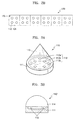
- the light emitting elements may be packaged in various structures, and several examples thereof are illustrated in Figures 3A, 3B, and 3C.
- a plurality of light emitting elements 112 are arranged on a base 111, and a cap 113 is disposed above the light emitting elements 112.
- the light emitting elements 112 are light emitting elements for emitting light having at least two different wavelengths.
- the light emitting elements 112 include a first light emitting element 112a for emitting light in a red wavelength range, a second light emitting element 112b for emitting light in a green wavelength range, and a third light emitting element 112c for emitting light in a blue wavelength range.
- the light emitting elements 112 include eight light emitting elements, that is, first, three light emitting elements 112a, second, two light emitting elements 112b, and third, three light emitting elements 112c.
- the number or arrangement shape of light emitting elements for each wavelength range can be changed according to a desired color temperature range in consideration of the amount of light emitted from light emitting elements for each wavelength range. Consistent with the present invention, since the degree of freedom that light emitting elements for emitting light in a plurality of wavelength ranges are formed in various arrangement methods and arrangement numbers and can be set as light emitting elements is large, colors can be easily realized and a manufacturer can select colors in a wide range. In addition, even when light emitting elements are configured in a multi-chip structure, the size of the light emitting elements is not greatly changed compared to light emitting diodes having single chips, there is no reason to worry about a volume increase.
- the cap 113 is formed of a transparent material having a larger refraction index than an adjacent external medium and may be a lens, for example.
- the cap 113 is shown formed in a conic shape, it is not limited to this shape and can be formed in various other shapes.
- a light emitting element 110' illustrated in Figure 3B includes a dome-shaped cap 114, or a light emitting element 110" illustrated in Figure 3C includes a polygonal pyramid cap.
- a plurality of light emitting elements 135 are disposed on a rectangular base 130 and a pyramid cap 132 is disposed above the base 130.
- the light emitting elements 112 and 135 are not disposed in the center of the bases 111 and 130, but rather on inner circumferences of the base 111 and 130.
- the light emitting elements are not disposed in the center of the bases 111 and 130 so that spots can be prevented from being formed.
- the spots are formed when light emitted from a light emitting element is not uniformly diffused and irradiated at relatively high brightness and shown as partially-bright spots and thus cause the image quality to be degraded.
- a display includes a backlight unit 150 and a display panel 170 for forming an image using light irradiated from the backlight unit 150.
- the backlight unit 150 includes a light emitting assembly 120 assembled in light emitting modules 100 and a light guide panel 140 for guiding light irradiated from the light emitting assembly 120 to be directed to the display panel 170.
- a diffusion panel 153 for diffusing light, a prism sheet 155 for correcting the path of light, and a brightness enhancement film (BEF) 157 for enhancing directivity so as to make light passing through the prism sheet 155 be directed to the display panel 170 are disposed between the light guide panel 140 and the display panel 170.
- the BEF 157 refracts and condenses light emitting from the diffusion panel 153 to enhance the directivity of light, thereby increasing brightness.
- the display panel 170 may be a liquid crystal panel, for example.
- a polarization enhancement film 160 for enhancing polarization efficiency may be further disposed above the BEF 157.
- the polarization enhancement film 160 transmits p-polarized light and reflects s-polarized light so that most of the incident light is emitted as light polarized in one direction, for example, p-polarized light.
- a prism pattern 145 may be formed on the bottom surface of the light guide panel 140.
- the prism pattern 145 prevents the intensity of light, when light emitted from the light emitting assembly 120 is reflected through the light guide panel 140, from being decreased as the prism pattern 145 is distant from the light emitting assembly 120, thereby enhancing uniformity of light.
- the prism pattern 145 is more densely arranged as it is distant from the light emitting assembly 120.
- the prism pattern 145 may be symmetrical with the center line of the light guide panel 140.
- the light emitting assembly consistent with the present invention can be assembled in various shapes according to the size of a display screen using blocked light emitting modules and thus can be very efficiently used.
- the magnitude of current to be supplied to light emitting modules disposed at the edges of the light emitting assembly can be larger than that of current to be supplied to the remaining light emitting modules. This is because the supply of current can be controlled independently in each light emitting module.
- the light assembly consistent with the present invention can be used in a direct light type backlight unit besides an edge light type backlight unit.
- the light emitting assembly according to the present invention can be assembled using light emitting modules comprised of independent blocks and thus, can be freely used regardless of the size of the display screen and when defective elements occur, the light emitting assembly can be easily replaced with another one.
- different production lines don't need to be disposed to produce light sources used in a backlight unit according to the size of a display screen manufacturing costs can be remarkably reduced.
- light emitting modules can be independently driven, a relatively large current is supplied to the light emitting modules disposed at edges of the light emitting assembly compared to other light emitting modules such that spots can be prevented from being formed at the edges.
- the size of a light emitting assembly is selected and thus can be widely used in the backlight unit and the display.
Landscapes
- Physics & Mathematics (AREA)
- Nonlinear Science (AREA)
- General Physics & Mathematics (AREA)
- Optics & Photonics (AREA)
- Mathematical Physics (AREA)
- Chemical & Material Sciences (AREA)
- Crystallography & Structural Chemistry (AREA)
- Engineering & Computer Science (AREA)
- General Engineering & Computer Science (AREA)
- Microelectronics & Electronic Packaging (AREA)
- Theoretical Computer Science (AREA)
- Planar Illumination Modules (AREA)
- Led Device Packages (AREA)
- Devices For Indicating Variable Information By Combining Individual Elements (AREA)
Abstract
Description
- The present invention relates to a light emitting assembly that can be easily assembled according to the size of display to be used as a light source, a backlight unit and a display having the same.
- In general, liquid crystal display (LCD) devices which are a type of flat panel displays are light receiving type displays that are not self-luminescent but form an image using incident light from the outside. LCD devices are used in notebooks, desktop computers, LCD-TVs, and mobile communication terminals and require backlight units besides liquid crystal panels. Backlight units are installed on a rear side of the LCD device and radiate light onto a liquid crystal panel.
- Backlight units can be mainly classified into direct light type backlight units that radiate light emitted from a plurality of light sources directly installed under an LCD device onto a liquid crystal panel, and edge light type backlight units that transmit light emitted from a light source installed at sidewalls of a light guide panel (LGP) onto the liquid crystal panel, according to the arrangement of a light source. A cold cathode fluorescent lamp (CCFL) is used as a light source in edge light type backlight units. The CCFL has low color reproduction and thus is not suitable for a high picture-quality and high-resolution TV or monitor. Accordingly, a light emitting diode (LED) has been spotlighted as a light source that replaces the CCFL.
- Referring to Figure 1A, a conventional edge light
type backlight unit 20 includes a plurality ofLEDs 10 arranged on aPCB substrate 5 and alight guide panel 15 that guides light emitted from theLEDs 10 to be incident on a liquid crystal panel. TheLEDs 10 are arranged in a plurality of columns and rows, as illustrated in Figure 1B. TheLEDs 10 include LEDs that produce red, green, and blue colored light. The red, green, and blue colored light is mixed on thelight guide panel 15, thereby realizing white light. - However, in the conventional edge light type backlight unit, LEDs are arranged on a PCB substrate manufactured to a predetermined size according to the size of a display screen so as to produce a light source. Thus, since an LED substrate having different sizes should be manufactured according to the size of a display screen, a production line should be constituted according to the size of the display screen. Thus, manufacturing costs increase, and due to the size of the display screen, the frequency of the LED substrate that can be commonly used is reduced. In addition, when defects occur in a portion of LEDs, the entire LED substrate should be replaced and it is difficult to manage defects.
- According to the present invention there is provided an apparatus and method as set forth in the appended claims. Preferred features of the invention will be apparent from the dependent claims, and the description which follows.
- The present invention provides a light emitting module that can be effectively used regardless of the size of a display screen, a backlight unit and a display having the same.
- According to an aspect of the present invention, there is provided a light emitting assembly including light emitting modules, wherein the light emitting modules include: a substrate having an electrical connecting portion; and a plurality of light emitting units arranged on the substrate, and wherein the light emitting modules are operative to be assembled using the electrical connecting portion.
- The light emitting units may include at least one of:
- a base; a plurality of light emitting elements arranged on the base and irradiating light having at least two wavelengths; and a cap arranged above the light emitting elements and totally reflecting light emitted from the light emitting elements.
- The light emitting elements may not be disposed in a center of the base but on inner circumferences thereof.
- The cap may be in the form of, for example, a cone, a polygonal pyramid, and a dome.
- The light emitting elements may include: a first light emitting element irradiating light in a red wavelength region; a second light emitting element irradiating light in a green wavelength region; and a third light emitting element irradiating light in a blue wavelength region.
- According to another aspect of the present invention, there is provided a backlight unit irradiating light onto a display, the backlight unit including: a light emitting assembly having light emitting modules, wherein the light emitting modules include: a substrate having an electrical connecting portion; and a plurality of light emitting units arranged on the substrate, and wherein the light emitting modules are operative to be assembled using the electrical connecting portion; and a light guide panel guiding light emitted from the light emitting assembly.
- According to another aspect of the present invention, there is provided a display, the display including: a backlight unit, wherein the backlight unit includes: a light emitting assembly having light emitting modules, wherein the light emitting modules include: a substrate having an electrical connecting portion; and a plurality of light emitting units arranged on the substrate, and wherein the light emitting modules are operative to be assembled using the electrical connecting portion; and a light guide panel guiding light emitted from the light emitting assembly; and a display panel forming an image using light irradiated from the backlight unit.
- The above and other features and advantages of the present invention will become more apparent by describing in detail exemplary embodiments thereof with reference to the attached drawings, in which:
- Figure 1A illustrates a conventional edge light type backlight unit;
- Figure 1B illustrates a light source illustrated in Figure 1A;
- Figure 2A illustrates a light emitting module used in a light emitting assembly according to an exemplary embodiment of the present invention;
- Figure 2B illustrates a light emitting assembly according to an exemplary embodiment of the present invention;
- Figures 3A through 3C illustrate examples of light emitting units used in the light emitting module illustrated in Figure 2A, respectively; and
- Figure 4 is a schematic view of a display according to an exemplary embodiment of the present invention.
- Referring to Figures 2A and 2B, a
light emitting assembly 120 according to an exemplary embodiment of the present invention can be configured to a desired size by connecting a plurality oflight emitting modules 100 that can be assembled. Each of thelight emitting modules 100 includes a plurality oflight emitting elements 110 arranged on asubstrate 105 and electrical connectingportions light emitting modules 100 to thesubstrate 105. Theelectrical connecting portions portion 115 and a second connectingportion 116 that can be pair-combined so as to connect adjacent light emitting modules. The number of thelight emitting elements 110 shown in Figure 2A is 4, but is not limited to this number and can be changed in various ways. - The
substrate 105 may be a printed circuit board (PCB). When thesubstrate 105 is manufactured as a PCB, an additional PCB is not required and thus, a structure of thelight emitting assembly 120 can be further simplified. An additional PCB can also be used and thelight emitting modules 100 can be combined with one another on the PCB. - The
light emitting modules 100 may be multi-chip light emitting elements having a plurality of light emitting elements for irradiating light having at least two wavelengths. The light emitting elements may be light emitting diodes (LEDs), for example. In addition, each of the light emitting elements includes a cap for total reflecting light irradiated from the light emitting elements and totally reflects light having different wavelengths emitted from the light emitting elements several times inside the light emitting elements, thereby mixing light. - The light emitting elements may be packaged in various structures, and several examples thereof are illustrated in Figures 3A, 3B, and 3C. In the
light emitting elements 110 illustrated in Figure 3A, a plurality oflight emitting elements 112 are arranged on abase 111, and acap 113 is disposed above thelight emitting elements 112. - The
light emitting elements 112 are light emitting elements for emitting light having at least two different wavelengths. For example, thelight emitting elements 112 include a firstlight emitting element 112a for emitting light in a red wavelength range, a secondlight emitting element 112b for emitting light in a green wavelength range, and a thirdlight emitting element 112c for emitting light in a blue wavelength range. - In Figure 3A, the
light emitting elements 112 include eight light emitting elements, that is, first, threelight emitting elements 112a, second, twolight emitting elements 112b, and third, threelight emitting elements 112c. The number or arrangement shape of light emitting elements for each wavelength range can be changed according to a desired color temperature range in consideration of the amount of light emitted from light emitting elements for each wavelength range. Consistent with the present invention, since the degree of freedom that light emitting elements for emitting light in a plurality of wavelength ranges are formed in various arrangement methods and arrangement numbers and can be set as light emitting elements is large, colors can be easily realized and a manufacturer can select colors in a wide range. In addition, even when light emitting elements are configured in a multi-chip structure, the size of the light emitting elements is not greatly changed compared to light emitting diodes having single chips, there is no reason to worry about a volume increase. - Light emitted from the light emitting elements passes through the
cap 113 and is totally reflected inside thecap 113 several times and mixed with one another. Thecap 113 is formed of a transparent material having a larger refraction index than an adjacent external medium and may be a lens, for example. In addition, while thecap 113 is shown formed in a conic shape, it is not limited to this shape and can be formed in various other shapes. For example, a light emitting element 110' illustrated in Figure 3B includes a dome-shaped cap 114, or alight emitting element 110" illustrated in Figure 3C includes a polygonal pyramid cap. In Figure 3C, a plurality oflight emitting elements 135 are disposed on arectangular base 130 and apyramid cap 132 is disposed above thebase 130. - The
light emitting elements bases base bases bases caps caps bases caps caps caps bases caps caps - Since light having different wavelengths emitted from the
light emitting elements caps caps - Referring to Figure 4, a display includes a
backlight unit 150 and adisplay panel 170 for forming an image using light irradiated from thebacklight unit 150. Thebacklight unit 150 includes alight emitting assembly 120 assembled inlight emitting modules 100 and alight guide panel 140 for guiding light irradiated from thelight emitting assembly 120 to be directed to thedisplay panel 170. - A
diffusion panel 153 for diffusing light, aprism sheet 155 for correcting the path of light, and a brightness enhancement film (BEF) 157 for enhancing directivity so as to make light passing through theprism sheet 155 be directed to thedisplay panel 170 are disposed between thelight guide panel 140 and thedisplay panel 170. TheBEF 157 refracts and condenses light emitting from thediffusion panel 153 to enhance the directivity of light, thereby increasing brightness. - The
display panel 170 may be a liquid crystal panel, for example. When thedisplay panel 170 is a liquid crystal panel, apolarization enhancement film 160 for enhancing polarization efficiency may be further disposed above theBEF 157. Thepolarization enhancement film 160 transmits p-polarized light and reflects s-polarized light so that most of the incident light is emitted as light polarized in one direction, for example, p-polarized light. - A
prism pattern 145 may be formed on the bottom surface of thelight guide panel 140. Theprism pattern 145 prevents the intensity of light, when light emitted from thelight emitting assembly 120 is reflected through thelight guide panel 140, from being decreased as theprism pattern 145 is distant from thelight emitting assembly 120, thereby enhancing uniformity of light. Theprism pattern 145 is more densely arranged as it is distant from thelight emitting assembly 120. In addition, when thelight emitting assembly 120 is disposed at both sides of thelight guide panel 140, theprism pattern 145 may be symmetrical with the center line of thelight guide panel 140. - As described above, the light emitting assembly consistent with the present invention can be assembled in various shapes according to the size of a display screen using blocked light emitting modules and thus can be very efficiently used. In addition, in order to improve relatively low brightness at edges of the backlight unit, the magnitude of current to be supplied to light emitting modules disposed at the edges of the light emitting assembly can be larger than that of current to be supplied to the remaining light emitting modules. This is because the supply of current can be controlled independently in each light emitting module.
- Furthermore, the light assembly consistent with the present invention can be used in a direct light type backlight unit besides an edge light type backlight unit.
- The light emitting assembly according to the present invention can be assembled using light emitting modules comprised of independent blocks and thus, can be freely used regardless of the size of the display screen and when defective elements occur, the light emitting assembly can be easily replaced with another one. Thus, since different production lines don't need to be disposed to produce light sources used in a backlight unit according to the size of a display screen, manufacturing costs can be remarkably reduced. Furthermore, since light emitting modules can be independently driven, a relatively large current is supplied to the light emitting modules disposed at edges of the light emitting assembly compared to other light emitting modules such that spots can be prevented from being formed at the edges.
- The size of a light emitting assembly is selected and thus can be widely used in the backlight unit and the display.
- Although a few preferred embodiments have been shown and described, it will be appreciated by those skilled in the art that various changes and modifications might be made without departing from the scope of the invention, as defined in the appended claims.
- Attention is directed to all papers and documents which are filed concurrently with or previous to this specification in connection with this application and which are open to public inspection with this specification, and the contents of all such papers and documents are incorporated herein by reference.
- All of the features disclosed in this specification (including any accompanying claims, abstract and drawings), and/or all of the steps of any method or process so disclosed, may be combined in any combination, except combinations where at least some of such features and/or steps are mutually exclusive.
- Each feature disclosed in this specification (including any accompanying claims, abstract and drawings) may be replaced by alternative features serving the same, equivalent or similar purpose, unless expressly stated otherwise. Thus, unless expressly stated otherwise, each feature disclosed is one example only of a generic series of equivalent or similar features.
- The invention is not restricted to the details of the foregoing embodiment(s). The invention extends to any novel one, or any novel combination, of the features disclosed in this specification (including any accompanying claims, abstract and drawings), or to any novel one, or any novel combination, of the steps of any method or process so disclosed.
Claims (17)
- A light emitting assembly (120) comprising light emitting modules (100), wherein
the light emitting modules (100) comprise:a substrate (105) having an electrical connecting portion (115); anda plurality of light emitting units (110) arranged on the substrate (105), andwherein the light emitting modules (100) are operative to be assembled using the electrical connecting portion (115) . - The light emitting assembly (120) of claim 1, wherein the light emitting units (110) comprises:a base (111);a plurality of light emitting elements (112) arranged on the base (111) for irradiating light having at least two wavelengths; anda cap (113) arranged above the light emitting elements (112) and totally reflecting light emitted from the light emitting elements (112).
- The light emitting assembly (120) of claim 2, wherein the light emitting elements (112) are not disposed in a center of the base (111) but on inner circumferences thereof.
- The light emitting assembly (120) of claim 2 or 3, wherein the cap (113) is in the form of a cone, a polygonal pyramid, or a dome.
- The light emitting assembly (120) of claim 2, 3 or 4, wherein the cap (113) comprises a lens.
- The light emitting assembly (120) of any of claims 2 to 5, wherein the light emitting elements (112) comprise:a first light emitting element (112a) to irradiate light in a red wavelength region;a second light emitting element (112b) to irradiate light in a green wavelength region; anda third light emitting element (112c) to irradiate light in a blue wavelength region.
- The light emitting assembly (120) of any preceding claim, wherein the substrate (105) comprises a printed circuit board (PCB).
- A backlight unit (150) for irradiating light onto a display, the backlight unit (150) comprising:a light emitting assembly (120) having light emitting modules (100), wherein the light emitting modules (100) comprise:a substrate (105) having an electrical connecting portion (115); anda plurality of light emitting units (110) arranged on the substrate (105), andwherein the light emitting modules (100) are operative to be assembled using the electrical connecting portion (115); anda light guide panel (140) for guiding light emitted from the light emitting assembly (120).
- The backlight unit (150) of claim 8, further comprising a diffusion panel (153) disposed above the light guide panel (140) and for diffusing and transmitting incident light.
- The backlight unit (150) of claim 8 or 9, wherein the light emitting units (110) comprises:a base (111);a plurality of light emitting elements (112) arranged on the base (111) and irradiating light having at least two wavelengths; anda cap (113) arranged above the light emitting elements (112) and totally reflecting light emitted from the light emitting elements (112).
- The backlight unit (150) of claim 10, wherein the light emitting elements (112) are not disposed in a center of the base (111) but on inner circumferences thereof.
- The backlight unit (150) of claim 10 or 11, wherein the cap (113) is in the form of a cone, a polygonal pyramid, or a dome.
- The backlight unit (150) of claim 10, 11 or 12, wherein the cap (113) comprises a lens.
- The backlight unit (150) of any of claims 10 to 13, wherein the light emitting elements (112) comprise:a first light emitting element (112a) irradiating light in a red wavelength region;a second light emitting element (112b) irradiating light in a green wavelength region; anda third light emitting element (112c) irradiating light in a blue wavelength region.
- A display comprising:a backlight unit (150), wherein the backlight unit (150) comprises:a light emitting assembly (120) having light emitting modules (100), wherein the light emitting modules (100) comprise:a substrate (105) having an electrical connecting portion (115); anda plurality of light emitting units (110) arranged on the substrate (105), andwherein the light emitting modules (100) are operative to be assembled using the electrical connecting portion (115); anda light guide panel (140) guiding light emitted from the light emitting assembly (120); anda display panel (170) forming an image using light irradiated from the backlight unit (150).
- The display of claim 15, further comprising a diffusion panel (153) disposed above the light guide panel (140) and diffusing and transmitting incident light.
- The display of claim 15 or 16, wherein the light emitting units (110) comprises:a base (111);a plurality of light emitting elements (112) arranged on the base (111) and irradiating light having at least two wavelengths; anda cap (113) arranged above the light emitting elements (112) and totally reflecting light emitted from the light emitting elements (112).
Applications Claiming Priority (2)
| Application Number | Priority Date | Filing Date | Title |
|---|---|---|---|
| US66419305P | 2005-03-23 | 2005-03-23 | |
| KR1020050086242A KR100750130B1 (en) | 2005-03-23 | 2005-09-15 | Light emitting assembly, backlight unit and display |
Publications (2)
| Publication Number | Publication Date |
|---|---|
| EP1705514A1 true EP1705514A1 (en) | 2006-09-27 |
| EP1705514B1 EP1705514B1 (en) | 2012-02-08 |
Family
ID=36587414
Family Applications (1)
| Application Number | Title | Priority Date | Filing Date |
|---|---|---|---|
| EP06111516A Expired - Lifetime EP1705514B1 (en) | 2005-03-23 | 2006-03-21 | Light emitting assembly, backlight unit and display having the same |
Country Status (4)
| Country | Link |
|---|---|
| US (1) | US7447416B2 (en) |
| EP (1) | EP1705514B1 (en) |
| KR (1) | KR100750130B1 (en) |
| CN (1) | CN1837922A (en) |
Cited By (2)
| Publication number | Priority date | Publication date | Assignee | Title |
|---|---|---|---|---|
| WO2008146229A2 (en) | 2007-05-29 | 2008-12-04 | Koninklijke Philips Electronics N.V. | Illumination system, luminaire and backlighting unit |
| TWI596407B (en) * | 2010-09-03 | 2017-08-21 | Lg伊諾特股份有限公司 | Backlight unit |
Families Citing this family (16)
| Publication number | Priority date | Publication date | Assignee | Title |
|---|---|---|---|---|
| KR100705702B1 (en) * | 2005-10-24 | 2007-04-09 | 주식회사 나모텍 | Color mixing lens for display and backlight device equipped with the same |
| KR100786096B1 (en) * | 2006-09-26 | 2007-12-21 | 엘지전자 주식회사 | Backlight Unit and Its Printed Circuit Board |
| KR101498682B1 (en) * | 2008-08-20 | 2015-03-04 | 삼성전자주식회사 | Light emitting diode module |
| CN102149966B (en) * | 2008-09-12 | 2014-03-12 | 皇家飞利浦电子股份有限公司 | Luminaire and illumination system |
| TWI394916B (en) * | 2009-09-28 | 2013-05-01 | Hannstar Display Corp | Light emitting unit, backlight module and displaying device |
| TW201126764A (en) * | 2010-01-25 | 2011-08-01 | Icp Technology Co Ltd | Method for manufacturing light-emitting diode with substrate having fine perforations and light-emitting diode |
| KR20130046042A (en) * | 2011-10-27 | 2013-05-07 | 삼성전자주식회사 | Backlight unit and display apparatus having the same |
| US9395052B1 (en) * | 2012-11-13 | 2016-07-19 | Larry N. Shew | Modular lighting assembly |
| TW201422968A (en) * | 2012-12-11 | 2014-06-16 | Hon Hai Prec Ind Co Ltd | LED lamp |
| CN103016990B (en) * | 2012-12-21 | 2014-11-05 | 广东爱华新光电科技有限公司 | LED (Light Emitting Diode) lamp tube assembly |
| CN103900012A (en) * | 2014-04-17 | 2014-07-02 | 南宁桂格精工科技有限公司 | Daytime traveling crane lamp set capable of being combined at will |
| CN104048217A (en) * | 2014-06-24 | 2014-09-17 | 深圳市华星光电技术有限公司 | Direct-type backlight module and liquid crystal display device |
| CN104819430A (en) * | 2015-04-29 | 2015-08-05 | 武汉华星光电技术有限公司 | Tri-phosphor light emitting module, backlight module and liquid crystal display panel |
| US10544920B2 (en) * | 2015-05-04 | 2020-01-28 | Signify Holding B.V. | Repeatable louver accessory for luminaires |
| EP3894741B1 (en) * | 2018-12-13 | 2023-02-15 | Lumileds LLC | Automotive headlight with dual correlated colour temperature |
| CN111885820B (en) * | 2020-08-07 | 2021-12-31 | 珠海格力电器股份有限公司 | Electric appliance, controller, control panel and panel unit thereof |
Citations (6)
| Publication number | Priority date | Publication date | Assignee | Title |
|---|---|---|---|---|
| JP2000353405A (en) * | 1999-06-08 | 2000-12-19 | Shinichi Kobayashi | Lamps composed of red, blue and green light emitting diode (LED) chips |
| EP1162400A2 (en) * | 2000-06-09 | 2001-12-12 | Omnilux s.r.l. | Modular lighting elements with leds (light-emitting diodes) |
| US20020135298A1 (en) | 2001-03-26 | 2002-09-26 | Pelka David G. | Light extractor apparatus |
| US20040032388A1 (en) * | 2002-08-16 | 2004-02-19 | Toppoly Optoelectronics Corp. | Backlight device of a LCD display |
| DE10242292A1 (en) * | 2002-09-12 | 2004-04-01 | Sebastian Matthias | Luminaire comprising LEDs in receptacle within frame, has frame with securing pieces for attaching and/or electrically connecting second luminaire |
| US20040228127A1 (en) | 2003-05-16 | 2004-11-18 | Squicciarini John B. | LED clusters and related methods |
Family Cites Families (34)
| Publication number | Priority date | Publication date | Assignee | Title |
|---|---|---|---|---|
| JPS6184880A (en) | 1984-10-02 | 1986-04-30 | Sharp Corp | Solid-state light emitting display |
| US5822053A (en) * | 1995-04-25 | 1998-10-13 | Thrailkill; William | Machine vision light source with improved optical efficiency |
| JP4007461B2 (en) * | 1996-07-24 | 2007-11-14 | シチズン電子株式会社 | Color display device |
| KR100421900B1 (en) | 1997-04-09 | 2004-04-17 | 엘지.필립스 엘시디 주식회사 | back light of liquid grystal display device |
| KR19990023425U (en) * | 1997-12-05 | 1999-07-05 | 손욱 | Optical module using light emitting diode |
| JP2000068562A (en) | 1998-08-21 | 2000-03-03 | Stanley Electric Co Ltd | Led lamp |
| KR100682563B1 (en) | 1999-07-26 | 2007-02-15 | 라보 스피아 가부시키가이샤 | Bulk lens, light emitting body, lighting device and optical information system |
| JP4352522B2 (en) * | 1999-09-01 | 2009-10-28 | ソニー株式会社 | Light-emitting flat display element |
| KR20010097147A (en) * | 2000-04-20 | 2001-11-08 | 박득일 | Back Light Unit by Use of White LED and Emission Method of White Light in High Purity |
| JP4545281B2 (en) * | 2000-05-24 | 2010-09-15 | アビックス株式会社 | Panel type LED display module |
| KR20020041480A (en) | 2000-11-28 | 2002-06-03 | 유순재 | Back-light source module of liquid crystal display |
| DE10060653A1 (en) | 2000-12-06 | 2002-06-20 | Epcos Ag | Electric double layer capacitor |
| KR100788382B1 (en) * | 2000-12-13 | 2007-12-31 | 엘지.필립스 엘시디 주식회사 | Backlight Unit of LCD |
| JP4674418B2 (en) | 2001-06-29 | 2011-04-20 | パナソニック株式会社 | Lighting equipment |
| JP4067801B2 (en) * | 2001-09-18 | 2008-03-26 | 松下電器産業株式会社 | Lighting device |
| JP4067802B2 (en) * | 2001-09-18 | 2008-03-26 | 松下電器産業株式会社 | Lighting device |
| US20030076034A1 (en) * | 2001-10-22 | 2003-04-24 | Marshall Thomas M. | Led chip package with four led chips and intergrated optics for collimating and mixing the light |
| JP3766042B2 (en) | 2002-06-21 | 2006-04-12 | 三菱電機株式会社 | Rear light source for display device and liquid crystal display device |
| CN2544172Y (en) | 2002-08-14 | 2003-04-09 | 崔淑萍 | Automatic color gradually changing multi-color lamp |
| DE10245580B4 (en) * | 2002-09-27 | 2006-06-01 | Siemens Ag | Device for generating an image |
| GB0227632D0 (en) | 2002-11-27 | 2003-01-08 | Koninkl Philips Electronics Nv | Active matrix display |
| JP4526807B2 (en) | 2002-12-24 | 2010-08-18 | 日本ペイント株式会社 | Pre-painting method |
| ES2316706T3 (en) | 2002-12-24 | 2009-04-16 | Chemetall Gmbh | METHOD OF PRE-TREATMENT TO COVER. |
| JP2004233809A (en) | 2003-01-31 | 2004-08-19 | Seiko Epson Corp | Surface light source unit, electro-optical device and electronic apparatus using the same |
| JP2004246117A (en) | 2003-02-14 | 2004-09-02 | Matsushita Electric Ind Co Ltd | Backlight device |
| JP4504662B2 (en) * | 2003-04-09 | 2010-07-14 | シチズン電子株式会社 | LED lamp |
| KR100508245B1 (en) | 2003-04-16 | 2005-08-17 | 엘지.필립스 엘시디 주식회사 | Liquid crystal module and driving apparatus and method thereof |
| KR20040096186A (en) | 2003-05-07 | 2004-11-16 | 엘지.필립스 엘시디 주식회사 | Back light unit and liquid crystal display device by using the same |
| US7394448B2 (en) * | 2003-06-20 | 2008-07-01 | Lg. Display Co., Ltd | Method and apparatus for driving liquid crystal display device |
| KR100954330B1 (en) * | 2003-06-24 | 2010-04-21 | 엘지디스플레이 주식회사 | LCD using light emitting diode |
| TWI244535B (en) * | 2004-03-24 | 2005-12-01 | Yuan Lin | A full color and flexible illuminating strap device |
| US7602369B2 (en) * | 2004-05-04 | 2009-10-13 | Sharp Laboratories Of America, Inc. | Liquid crystal display with colored backlight |
| KR100619069B1 (en) * | 2005-02-16 | 2006-08-31 | 삼성전자주식회사 | Multichip Light Emitting Diode Unit, Backlight Unit and Liquid Crystal Display Apparatus |
| KR20060095345A (en) * | 2005-02-28 | 2006-08-31 | 엘지.필립스 엘시디 주식회사 | Backlight Assembly and Liquid Crystal Display Using Same |
-
2005
- 2005-09-15 KR KR1020050086242A patent/KR100750130B1/en not_active Expired - Fee Related
-
2006
- 2006-03-21 EP EP06111516A patent/EP1705514B1/en not_active Expired - Lifetime
- 2006-03-22 CN CNA2006100585985A patent/CN1837922A/en active Pending
- 2006-03-23 US US11/386,785 patent/US7447416B2/en not_active Expired - Fee Related
Patent Citations (6)
| Publication number | Priority date | Publication date | Assignee | Title |
|---|---|---|---|---|
| JP2000353405A (en) * | 1999-06-08 | 2000-12-19 | Shinichi Kobayashi | Lamps composed of red, blue and green light emitting diode (LED) chips |
| EP1162400A2 (en) * | 2000-06-09 | 2001-12-12 | Omnilux s.r.l. | Modular lighting elements with leds (light-emitting diodes) |
| US20020135298A1 (en) | 2001-03-26 | 2002-09-26 | Pelka David G. | Light extractor apparatus |
| US20040032388A1 (en) * | 2002-08-16 | 2004-02-19 | Toppoly Optoelectronics Corp. | Backlight device of a LCD display |
| DE10242292A1 (en) * | 2002-09-12 | 2004-04-01 | Sebastian Matthias | Luminaire comprising LEDs in receptacle within frame, has frame with securing pieces for attaching and/or electrically connecting second luminaire |
| US20040228127A1 (en) | 2003-05-16 | 2004-11-18 | Squicciarini John B. | LED clusters and related methods |
Non-Patent Citations (1)
| Title |
|---|
| PATENT ABSTRACTS OF JAPAN vol. 2000, no. 15 6 April 2001 (2001-04-06) * |
Cited By (5)
| Publication number | Priority date | Publication date | Assignee | Title |
|---|---|---|---|---|
| WO2008146229A2 (en) | 2007-05-29 | 2008-12-04 | Koninklijke Philips Electronics N.V. | Illumination system, luminaire and backlighting unit |
| WO2008146229A3 (en) * | 2007-05-29 | 2009-02-12 | Koninkl Philips Electronics Nv | Illumination system, luminaire and backlighting unit |
| US8425101B2 (en) | 2007-05-29 | 2013-04-23 | Koninklijke Philips Electronics N.V. | Illumination system, luminaire and backlighting unit |
| EP2843464A1 (en) * | 2007-05-29 | 2015-03-04 | Koninklijke Philips N.V. | Lighting device having a light exit window |
| TWI596407B (en) * | 2010-09-03 | 2017-08-21 | Lg伊諾特股份有限公司 | Backlight unit |
Also Published As
| Publication number | Publication date |
|---|---|
| EP1705514B1 (en) | 2012-02-08 |
| KR20060102472A (en) | 2006-09-27 |
| CN1837922A (en) | 2006-09-27 |
| US7447416B2 (en) | 2008-11-04 |
| KR100750130B1 (en) | 2007-08-21 |
| US20060215405A1 (en) | 2006-09-28 |
Similar Documents
| Publication | Publication Date | Title |
|---|---|---|
| JP4589361B2 (en) | Light source cube, flat light source unit and liquid crystal display device using the same | |
| US7447416B2 (en) | Light emitting assembly, backlight unit and display having the same | |
| US7554625B2 (en) | Display device and backlight device having plural solid-state emitting element units each emitting at least three colors and contained within a cylindrical air-filled light guide body also surrounded by air | |
| KR100619069B1 (en) | Multichip Light Emitting Diode Unit, Backlight Unit and Liquid Crystal Display Apparatus | |
| JP5066572B2 (en) | Backlight unit and liquid crystal display device including the same | |
| CN100447634C (en) | Direct-lit backlight unit and LCD display | |
| US8657478B2 (en) | Backlight module | |
| JP4350138B2 (en) | Edge type backlight unit | |
| TWI479234B (en) | Display apparatus | |
| US20090168455A1 (en) | Backlight unit for liquid crystal display device | |
| JP2004342587A (en) | Backlight and liquid crystal display device using the same | |
| CN102803821A (en) | Lighting device, display device and television receiving device | |
| US8094259B2 (en) | Liquid crystal display without color filter | |
| JP2007266590A (en) | Light source module, backlight device, and liquid crystal display device | |
| KR101294849B1 (en) | Backlight assemlby | |
| KR20170026883A (en) | Light Emitting Diode Lamp And Liquid Crystal Display Device Including The Same | |
| US20060203484A1 (en) | Light emitting diode, light emitting diode module, and related backlight system | |
| US20110242433A1 (en) | Lighting device, display device and television receiver | |
| KR101042698B1 (en) | Surface light source device | |
| US20130038798A1 (en) | Display device and television receiver | |
| US20110019130A1 (en) | Lcd including led | |
| KR101291958B1 (en) | Backlight unit and liquid crystal display device using the same | |
| WO2011074410A1 (en) | Illuminating device, display device, and television receiver | |
| KR102628674B1 (en) | Light emitting diode pakgage module and display device having the same | |
| KR101080098B1 (en) | Backlight panel for backlighting a display panel |
Legal Events
| Date | Code | Title | Description |
|---|---|---|---|
| PUAI | Public reference made under article 153(3) epc to a published international application that has entered the european phase |
Free format text: ORIGINAL CODE: 0009012 |
|
| 17P | Request for examination filed |
Effective date: 20060321 |
|
| AK | Designated contracting states |
Kind code of ref document: A1 Designated state(s): AT BE BG CH CY CZ DE DK EE ES FI FR GB GR HU IE IS IT LI LT LU LV MC NL PL PT RO SE SI SK TR |
|
| AX | Request for extension of the european patent |
Extension state: AL BA HR MK YU |
|
| 17Q | First examination report despatched |
Effective date: 20061102 |
|
| AKX | Designation fees paid |
Designated state(s): DE FR GB IT NL |
|
| GRAP | Despatch of communication of intention to grant a patent |
Free format text: ORIGINAL CODE: EPIDOSNIGR1 |
|
| RIN1 | Information on inventor provided before grant (corrected) |
Inventor name: SEONG, KI-BUM Inventor name: WANG, JONG-MIN Inventor name: CHO, TAE-HEE Inventor name: NOH, JI-WHAN Inventor name: KIM, SU-GUN Inventor name: JUNG, IL-YONG |
|
| GRAS | Grant fee paid |
Free format text: ORIGINAL CODE: EPIDOSNIGR3 |
|
| GRAA | (expected) grant |
Free format text: ORIGINAL CODE: 0009210 |
|
| AK | Designated contracting states |
Kind code of ref document: B1 Designated state(s): DE FR GB IT NL |
|
| REG | Reference to a national code |
Ref country code: GB Ref legal event code: FG4D |
|
| REG | Reference to a national code |
Ref country code: DE Ref legal event code: R096 Ref document number: 602006027513 Country of ref document: DE Effective date: 20120405 |
|
| REG | Reference to a national code |
Ref country code: NL Ref legal event code: T3 |
|
| RAP2 | Party data changed (patent owner data changed or rights of a patent transferred) |
Owner name: SAMSUNG ELECTRONICS CO., LTD. |
|
| PLBE | No opposition filed within time limit |
Free format text: ORIGINAL CODE: 0009261 |
|
| STAA | Information on the status of an ep patent application or granted ep patent |
Free format text: STATUS: NO OPPOSITION FILED WITHIN TIME LIMIT |
|
| 26N | No opposition filed |
Effective date: 20121109 |
|
| REG | Reference to a national code |
Ref country code: DE Ref legal event code: R097 Ref document number: 602006027513 Country of ref document: DE Effective date: 20121109 |
|
| REG | Reference to a national code |
Ref country code: FR Ref legal event code: PLFP Year of fee payment: 10 |
|
| PGFP | Annual fee paid to national office [announced via postgrant information from national office to epo] |
Ref country code: DE Payment date: 20150318 Year of fee payment: 10 Ref country code: NL Payment date: 20150319 Year of fee payment: 10 Ref country code: IT Payment date: 20150225 Year of fee payment: 10 |
|
| PGFP | Annual fee paid to national office [announced via postgrant information from national office to epo] |
Ref country code: FR Payment date: 20150320 Year of fee payment: 10 Ref country code: GB Payment date: 20150225 Year of fee payment: 10 |
|
| REG | Reference to a national code |
Ref country code: DE Ref legal event code: R119 Ref document number: 602006027513 Country of ref document: DE |
|
| REG | Reference to a national code |
Ref country code: NL Ref legal event code: MM Effective date: 20160401 |
|
| GBPC | Gb: european patent ceased through non-payment of renewal fee |
Effective date: 20160321 |
|
| REG | Reference to a national code |
Ref country code: FR Ref legal event code: ST Effective date: 20161130 |
|
| PG25 | Lapsed in a contracting state [announced via postgrant information from national office to epo] |
Ref country code: DE Free format text: LAPSE BECAUSE OF NON-PAYMENT OF DUE FEES Effective date: 20161001 Ref country code: GB Free format text: LAPSE BECAUSE OF NON-PAYMENT OF DUE FEES Effective date: 20160321 Ref country code: NL Free format text: LAPSE BECAUSE OF NON-PAYMENT OF DUE FEES Effective date: 20160401 Ref country code: FR Free format text: LAPSE BECAUSE OF NON-PAYMENT OF DUE FEES Effective date: 20160331 |
|
| PG25 | Lapsed in a contracting state [announced via postgrant information from national office to epo] |
Ref country code: IT Free format text: LAPSE BECAUSE OF NON-PAYMENT OF DUE FEES Effective date: 20160321 |