EP1701451A2 - Distortion compensation apparatus - Google Patents
Distortion compensation apparatus Download PDFInfo
- Publication number
- EP1701451A2 EP1701451A2 EP05253977A EP05253977A EP1701451A2 EP 1701451 A2 EP1701451 A2 EP 1701451A2 EP 05253977 A EP05253977 A EP 05253977A EP 05253977 A EP05253977 A EP 05253977A EP 1701451 A2 EP1701451 A2 EP 1701451A2
- Authority
- EP
- European Patent Office
- Prior art keywords
- distortion compensation
- input signal
- distortion
- signal
- coefficient
- Prior art date
- Legal status (The legal status is an assumption and is not a legal conclusion. Google has not performed a legal analysis and makes no representation as to the accuracy of the status listed.)
- Granted
Links
Images




Classifications
-
- H—ELECTRICITY
- H03—ELECTRONIC CIRCUITRY
- H03F—AMPLIFIERS
- H03F1/00—Details of amplifiers with only discharge tubes, only semiconductor devices or only unspecified devices as amplifying elements
- H03F1/32—Modifications of amplifiers to reduce non-linear distortion
- H03F1/3241—Modifications of amplifiers to reduce non-linear distortion using predistortion circuits
- H03F1/3258—Modifications of amplifiers to reduce non-linear distortion using predistortion circuits based on polynomial terms
-
- H—ELECTRICITY
- H03—ELECTRONIC CIRCUITRY
- H03F—AMPLIFIERS
- H03F1/00—Details of amplifiers with only discharge tubes, only semiconductor devices or only unspecified devices as amplifying elements
- H03F1/02—Modifications of amplifiers to raise the efficiency, e.g. gliding Class A stages, use of an auxiliary oscillation
- H03F1/0205—Modifications of amplifiers to raise the efficiency, e.g. gliding Class A stages, use of an auxiliary oscillation in transistor amplifiers
-
- H—ELECTRICITY
- H03—ELECTRONIC CIRCUITRY
- H03F—AMPLIFIERS
- H03F1/00—Details of amplifiers with only discharge tubes, only semiconductor devices or only unspecified devices as amplifying elements
- H03F1/32—Modifications of amplifiers to reduce non-linear distortion
- H03F1/3241—Modifications of amplifiers to reduce non-linear distortion using predistortion circuits
-
- H—ELECTRICITY
- H03—ELECTRONIC CIRCUITRY
- H03F—AMPLIFIERS
- H03F1/00—Details of amplifiers with only discharge tubes, only semiconductor devices or only unspecified devices as amplifying elements
- H03F1/32—Modifications of amplifiers to reduce non-linear distortion
- H03F1/3241—Modifications of amplifiers to reduce non-linear distortion using predistortion circuits
- H03F1/3247—Modifications of amplifiers to reduce non-linear distortion using predistortion circuits using feedback acting on predistortion circuits
-
- H—ELECTRICITY
- H03—ELECTRONIC CIRCUITRY
- H03F—AMPLIFIERS
- H03F2201/00—Indexing scheme relating to details of amplifiers with only discharge tubes, only semiconductor devices or only unspecified devices as amplifying elements covered by H03F1/00
- H03F2201/32—Indexing scheme relating to modifications of amplifiers to reduce non-linear distortion
- H03F2201/3233—Adaptive predistortion using lookup table, e.g. memory, RAM, ROM, LUT, to generate the predistortion
-
- H—ELECTRICITY
- H04—ELECTRIC COMMUNICATION TECHNIQUE
- H04B—TRANSMISSION
- H04B1/00—Details of transmission systems, not covered by a single one of groups H04B3/00 - H04B13/00; Details of transmission systems not characterised by the medium used for transmission
- H04B1/02—Transmitters
- H04B1/04—Circuits
- H04B2001/0408—Circuits with power amplifiers
- H04B2001/0425—Circuits with power amplifiers with linearisation using predistortion
Definitions
- the present invention relates to a distortion compensationapparatus,and moreparticularlyadistortion compensation apparatus which obtains a differential signal between a reference signal, that is, a transmission signal and a feedback signal, calculates a distortion compensation coefficient so as to reduce the differential signal by use of an adaptive algorithm, updates a distortion compensation coefficient having been stored using the above-calculated distortion compensation coefficient, and performs distortion compensation onto the transmission signal based on the above obtained distortion compensation coefficient.
- FIG. 1 shows an exemplary block diagram of transmission equipment in the conventional radio equipment.
- a transmission signal generator 1 outputs a digital serial data sequence.
- a serial-to-parallel (S/P) converter 2 then converts the digital data sequence into two series, in-phase component signals (I-signals) and quadrature component signals (Q-signals), by alternately distributing the digital data sequence on a bit-by-bit basis.
- I-signals in-phase component signals
- Q-signals quadrature component signals
- a digital-to-analog (D/A) converter 3 converts the I-signal and the Q-signal into an analog baseband signal, respectively, and supplies than to a quadrature modulator 4.
- This quadrature modulator 4 multiplies the input I-signal and Q-signal (a baseband transmission signal) by a reference carrier wave 8, and a carrier wave phase-shifted by 90° from the reference carrier wave 8, and adds the multiplied results, thus performing orthogonal transformation, and outputs the above signal.
- a frequency converter 5 mixes the quadrature modulation signal with a local oscillation signal, and converts the mixed signal into a radio frequency.
- a transmission power amplifier 6 performs power amplification of the radio frequency signal being output from frequency converter 5, and radiates to the air from an antenna 7.
- transmission equipment power is substantially large, as much as 10 mW to several tens of mW
- the input/output characteristic (having a distortion function f(p)) of transmission power amplifier 6 shows non-linearity, as shown by the dotted line in FIG. 2.
- This nonlinear characteristic produces a non-linear distortion.
- the frequency spectrum in the vicinity of a transmission frequency f 0 comes to have a raised sidelobe, shifted from the characteristic shown by the broken line (a) in FIG. 3.
- This produces a leak to adjacent channels, and adjacent interference. Namely, due to the nonlinear distortion shown in FIG. 2, the leak power of the transmitted wave in the adjacent frequency channels becomes large, as shown in FIG. 3.
- An ACPR represents the magnitude of leak power, being defined as a ratio of leak power to adjacent channels, which corresponds to a spectrum area in the adjacent channels sandwiched between the lines B and B' in FIG. 3, to the power in the channel of interest, which corresponds to a spectrum area between the lines A and A' .
- Such leaked power affects other channels as noise, and degrades the communication quality of the channel of interest. For this reason, a strict regulation has been established.
- the leak power is substantially small in a linear region of, for example, a power amplifier (refer to a linear region I in FIG. 2), and is substantially large in a nonlinear region II. Accordingly, in order to obtain a high-output transmission power amplifier, the linear region I has to be widened. However, this requires an amplifier having a larger capacity than is actually needed, which causes a disadvantageous problem in both cost and size of the apparatus. To cope with this problem, it has been proposed to add a distortion compensation function to radio equipment so as to compensate for the transmission power distortion.
- FIG. 4 shows a block diagram of transmission equipment having a digital nonlinear distortion compensation function by use of a DSP (digital signal processor).
- a digital data group (transmission signals) transmitted from transmission signal generator 1 is converted into two series, I-signals and Q-signals, in S/P converter 2, and then input to a distortion compensator 9 implemented by a DSP.
- the signal to which distortion process is performed in distortion compensator 9 is input into D/A converter 3.
- This D/A converter 3 converts the input I-signal and Q-signal into analog baseband signals, and inputs the converted signals into quadrature modulator 4.
- Quadrature modulator 4 performs quadrature modulation by multiplying the input I-signal and Q-signal by a reference carrier wave 8 and a carrier wave being phase-shifted by 90° from reference carrier wave 8, respectively.
- Quadrature modulator 4 performs quadrature modulation by adding the multiplication result, and outputs the modulated signal.
- a frequency converter 5 performs frequency conversion by mixing the quadrature modulation signal with a local oscillation signal.
- a transmission power amplifier 6 performs power amplification of the radio frequency signal being output from frequency converter 5, and radiates to the air from antenna 7.
- a portion of the transmission signal is input to a frequency converter 11 via a directional coupler 10, and input into a quadrature detector 12 after being frequency converted by the above frequency converter 11.
- Quadrature detector 12 performs quadrature detection by multiplying the input signal by a reference carrier wave, and by a signal being phase-shifted by 90° from the reference carrier wave, respectively.
- A/D analog-to-digital
- A/D converter 13 converts the input I-signal and Q-signal into digital signals, and inputs into distortion compensator 9.
- distortion compensation coefficient calculator 92 of distortion compensator 9 the pre-compensated transmission signal is compared with the feedback signal being demodulated in quadrature detector 12. Then, distortion compensator 9 calculates the distortion compensation coefficient h(p1) so that the difference of the above comparison values becomes zero, and updates the above-obtained coefficient having been stored in distortion compensation coefficient storage 90.
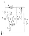
- FIG. 5 shows an explanation diagram when the distortion compensation processing is performed using the adaptive LMS algorithm in distortion compensator 9 shown in FIG. 4.
- a symbol 15a is a multiplier for multiplying a transmission signal x(t) by a distortion compensation coefficient h n-1 (p). This multiplier corresponds to the predistortion portion 91 shown in FIG. 4.
- 15b is a transmission power amplifier having a distortion function f(p)
- 15c is a feedback system in which feedback of output signal y(t) being output from transmission power amplifier 15b is performed.
- 15e is a distortion compensation coefficient storage (which corresponds to distortion compensation coefficient storage 90 shown in FIG. 4) for storing the distortion compensation coefficients each corresponding to each power of the transmission signal x(t).
- Distortion compensation coefficient storage 15e outputs a distortion compensation coefficient h n-1 (p) corresponding to the power p of the transmission signal x (t) .
- Distortion compensation coefficient storage 15e also updates a distortion compensation coefficient h n-1 (p) with a distortion compensation coefficient h n (p) obtained through the LMS algorithm.
- 15f is a conjugate complex signal output portion
- 15g is a subtractor outputting a difference e (t) between the transmission signal x(t) and the feedback demodulation signal y (t)
- 15h is a multiplier multiplying e (t) by u*(t)
- 15i is a multiplier multiplying h n-1 (p) by y*(t)
- 15j is a multiplier multiplying by a step size parameter ⁇
- 15k is an adder adding h n-1 (p) to ⁇ e (t) u* (t).
- 15m, 15n, 15p are delay portions by which a delay time D is added to the input signal.
- the delay time D denotes the time duration from the time the transmission signal x (t) is input to the time the feedback demodulation signal y(t) is input to subtractor 15g.
- Symbols 15f, 15h-15j constitute a calculation section 16.
- a signal y(t) is the signal after being distorted.
- x, y, f, h, u, e are complex numbers, and * denotes a conjugate complex number.
- the distortion compensation coefficient h (p) is updated so as to minimize the differential signal e(t) between the transmission signal x(t) and the feedback demodulation signal y(t). Finally, the value converges to an optimal distortion compensation coefficient, so that the distortion of the transmission power amplifier is compensated.
- the principle of the distortion compensation apparatus is that feedback detection of a carrier wave obtained after quadrature modulation of the transmission signal is performed, the amplitudes of the transmission signal and the feedback signal are compared after digital conversion, and a distortion compensation coefficient updated in real time based on the above comparison result. According to this nonlinear distortion compensation system, it is possible to reduce distortion, and leak power as well, even through the operation is performed in a nonlinear region with high output, and also to improve the power load efficiency.
- a correlation value is calculated varying the phases between a transmission signal x(t) and a feedback signal. Based on the maximum value of this correlation, a total delay time produced in a distortion device (transmission power amplifier), a feedback loop, etc. is determined. Then, the determined delay time is set in each delay circuit for timing adjustment in the distortion compensation apparatus.
- the distortion compensation operation is performed by the distortion compensation apparatus so as to reduce the difference between the transmission signal and the feedback signal.
- noise being output from the transmission power amplifier following the distortion compensation may possibly become larger than the noise being output therefrom prior to the distortion compensation, at the end region of the distortion compensation control bandwidth originally having a small distortion signal.
- the unwanted wave specified in the specification TS25.104 issued by the 3GPP (3rd Generation Partnership Project) it is required to reduce an unwanted wave so as to be sufficiently small at the frequency having a distance of a predetermined frequency offset amount from the transmission bandwidth.
- FIG. 6 shows a diagram concretely explaining the standard of the unwanted wave, in which a transmission signal spectrum exemplifying a case of four carriers is illustrated.
- a frequency F is indicated on the horizontal axis
- a transmission intensity SS is indicated on the vertical axis.
- the transmission signal output spectrum is shown in the case four carriers are set.
- transmission signals for four carriers are disposed within a transmission bandwidth SSBND1, and at the frequency having a distance of a frequency offset shown as OFFSET away from the end of the transmission bandwidth, it is required that an unwanted wave level shall be reduced for the value C or more from the level in the transmission bandwidth.
- a spectrum A indicates the spectrum prior to the distortion compensation having the transmission bandwidth SSBND1 of four carriers
- a spectrum B indicates the spectrum after performing distortion compensation explained in regard to FIG. 5.
- the floor level in the end region of the transmission bandwidth SSBND1 of four carriers is decreased.
- the floor is widened in the spectrum.
- FIG. 7 is a diagram illustrating a transmission signal output spectrum when the number of carriers is two.
- a transmission signal bandwidth SSBND2 becomes narrower than the transmission signal bandwidth SSBND1 in the case of four carriers shown in FIG. 6.
- a floor E of a spectrum B becomes widened, similar to the case of four carriers.
- the frequency having a distance of the frequency offset amount OFFSET specified in the standard of the unwanted wave is shifted to the left (nearer to the transmission bandwidth) as compared to FIG. 6.
- the unwanted wave level is increased at the frequency having a distance of the frequency offset amount specified in the standard of the unwanted wave.
- the specified condition that an unwanted wave level at the aforementioned frequency shall be reduced for the value C or more from the level in the transmission bandwidth is not met any more.
- the unwanted wave level has a value D, which is smaller than C, below the transmission bandwidth level.
- the distortion compensation may increase the unwanted radiation (inconformity to the standard of the unwanted wave), contrary to what is intended.
- a distortion compensation apparatus includes: a predistortion portion for distortion compensation processing of an input signal using a distortion compensation coefficient; a distortion compensation coefficient portion for storing the distortion compensation coefficient correspondingly to the input signal power, based on the input signal prior to the distortion compensation and a feedback signal being fed back from the output side of a distortion device; and a controller for reducing a distortion compensation control bandwidth in the predistortion portion, corresponding to the reduction of the number of input signal carriers.
- a distortion compensation apparatus includes: a distortion compensation processing circuit multiplying an input signal by a distortion compensation coefficient; a distortion compensation coefficient storage storing the distortion compensation coefficient correspondingly to the input signal power; a distortion compensation coefficient calculator calculating an update value of the distortion compensation coefficient stored in the distortion compensation coefficient storage, based on the input signal and a feedback signal being fed back from the output side of a distortion device; and a digital filter inputting the output of the distortion compensation processing circuit.
- the distortion compensation apparatus further include a unit for modifying the passband of the digital filter so as to reduce a distortion compensation control bandwidth in the predistortion portion, in response to the reduction of the number of carriers in the input signal.
- the modifying unit may include a memory storing a filter coefficient, and reads out, from the memory, the filter coefficient to be set for the digital filter passband corresponding to the number of carriers in the input signal, and sets the readout filter coefficient to the digital filter.
- the modifying unit may reduce a clock frequency for the distortion compensation apparatus, a D/A converter, an A/D converter, and a digital filter, in response to the reduction of the number of carriers in the input signal.
- the distortion device includes a controller operable to reduce a signal bandwidth to be input to the amplifier, when a signal transmission bandwidth is reduced.
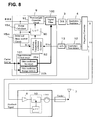
- FIG. 8 is a block diagram of transmission equipment having a digital nonlinear distortion compensation function in which the present invention is applied.
- like reference symbols refer to the like functional portions shown in FIGS. 4 and 5.
- a distortion compensation coefficient storage 90 is constituted of a look-up table, which is accessed using an input signal power value obtained in a power calculator 15d as an address.
- a distortion compensation coefficient calculator 92 is a functional portion for obtaining an update value of a distortion compensation coefficient to be stored in look-up table 90, based on the difference of a transmission signal S(x), a feedback signal R(x) and the correlation value therebetween.
- Distortion compensation coefficient calculator 92 includes a subtractor 15g and a calculation section 16, as shown in FIG. 5.
- a feedback system 15 shown in FIG. 5 corresponds to a feedback route beginning from an output of a power amplifier 6, and including frequency converter 11, demodulator 12 and A/D converter 13, etc., via a directional coupler 10.
- a distortion compensation apparatus 9 shown in FIG. 8 includes a supervision and control circuit 101 so as to enable variable setting of a pass bandwidth of a digital filter 100 based on a carrier set signal.
- the number of transmission carriers transmitted from a base station is input and set into a base station (a transmission parameter set section provided therein) as a transmission parameter, when the base station is newly installed or a system change is performed.
- a carrier set signal is input to supervision and control circuit 101.
- supervision and control circuit 101 also has functions of receiving input signal power information from power calculator 15d, supervising a state of the transmission equipment, and setting control parameters for a delay and phase control circuit 15m based on the correlation value between the input transmission signal and the feedback signal, as described in the official gazette of the Japanese Unexamined Patent Publication No. 2001-189685 (Patent document 1).
- supervision and control circuit 101 includes a filter coefficient set circuit 101a, to which a carrier set signal is input either from the transmission parameter set section of the base station, or through the operation from the operation section.
- Filter coefficient set circuit 101a has a function of referring to a table in a filter coefficient storage memory 101b, and reading out a corresponding filter coefficient from the table, based on the information of the number of carriers in the carrier set signal.
- Digital filter 100 functions as filter having a passband characteristic corresponding to the filter coefficient supplied thereto.
- digital filter 100 controls the passband thereof by setting the internal circuit according to the supplied filter coefficient. For example, after a tap coefficient group is supplied as filter coefficients, digital filter 100 operates to obtain a desired passband by setting the supplied tap coefficients to the respective taps. With this, when the transmission bandwidth is made narrower according to the carrier set signal, digital filter 100 can be modified to have a narrower passband.
- FIG. 9 is a diagram for explaining the passband control, illustrating a transmission signal output spectrum in the case of two carriers, as an embodiment example.
- digital filter 100 is so controlled as to have a narrower passband when two carriers are used as transmission signal than the passband being set into digital filter 100 in the case four carriers are used as transmission signal.
- a distortion compensation control bandwidth CBAND2 is narrower than a distortion compensation control bandwidth CBAND1.
- the reduced passband in digital filter 100 produces a reduced control bandwidth for predistortion processing, which undesirably weakens a distortion suppression effect, and increases an unwanted wave.
- a wide control bandwidth contrarily produces an increased noise component due to the incompleteness in the distortion compensation, and the influence of the unwanted wave is strengthened. Therefore, it is advantageous to reduce the control bandwidth from the viewpoint of suppressing the increase of the unwanted wave.
- control bandwidth of the distortion compensation is reduced when the number of carriers is small, so as to suppress an increase of the unwanted wave bandwidth caused by the incompleteness of the distortion compensation.
- the present invention has been devised to reduce the distortion compensation control bandwidth, so as to suppress the increase of the floor portion in the spectrum downstream of distortion compensation, when the number of set carriers is reduced.
- the distortion compensation control bandwidth can be controlled using a simple configuration, in response to either an increase or a decrease of the number of carriers being set in a transmitter. Even if the number of carriers decreases, an unwanted wave can easily be suppressed.
Landscapes
- Physics & Mathematics (AREA)
- Engineering & Computer Science (AREA)
- Power Engineering (AREA)
- Nonlinear Science (AREA)
- Algebra (AREA)
- General Physics & Mathematics (AREA)
- Mathematical Analysis (AREA)
- Mathematical Optimization (AREA)
- Pure & Applied Mathematics (AREA)
- Amplifiers (AREA)
- Digital Transmission Methods That Use Modulated Carrier Waves (AREA)
- Transmitters (AREA)
Abstract
Description
- The present invention relates to a distortion compensationapparatus,and moreparticularlyadistortion compensation apparatus which obtains a differential signal between a reference signal, that is, a transmission signal and a feedback signal, calculates a distortion compensation coefficient so as to reduce the differential signal by use of an adaptive algorithm, updates a distortion compensation coefficient having been stored using the above-calculated distortion compensation coefficient, and performs distortion compensation onto the transmission signal based on the above obtained distortion compensation coefficient.
- In recent years, high-efficient digital transmission has been adopted in radio communication. When multilevel phase modulation is adopted in the radio communication, it is an important technique to suppress nonlinear distortion by linearizing the amplification characteristic of a power amplifier on the transmission side, thereby reducing adjacent channel leak power.
- Also, when it is intended to improve power efficiency using an amplifier having a degraded linearity, a technique for compensating nonlinear distortion caused by the degraded linearity is essentially required.
- FIG. 1 shows an exemplary block diagram of transmission equipment in the conventional radio equipment. A
transmission signal generator 1 outputs a digital serial data sequence. A serial-to-parallel (S/P)converter 2 then converts the digital data sequence into two series, in-phase component signals (I-signals) and quadrature component signals (Q-signals), by alternately distributing the digital data sequence on a bit-by-bit basis. - A digital-to-analog (D/A)
converter 3 converts the I-signal and the Q-signal into an analog baseband signal, respectively, and supplies than to aquadrature modulator 4. Thisquadrature modulator 4 multiplies the input I-signal and Q-signal (a baseband transmission signal) by areference carrier wave 8, and a carrier wave phase-shifted by 90° from thereference carrier wave 8, and adds the multiplied results, thus performing orthogonal transformation, and outputs the above signal. - A
frequency converter 5 mixes the quadrature modulation signal with a local oscillation signal, and converts the mixed signal into a radio frequency. Atransmission power amplifier 6 performs power amplification of the radio frequency signal being output fromfrequency converter 5, and radiates to the air from anantenna 7. - Here, in the mobile communication using W-CDMA, etc., transmission equipment power is substantially large, as much as 10 mW to several tens of mW, and the input/output characteristic (having a distortion function f(p)) of
transmission power amplifier 6 shows non-linearity, as shown by the dotted line in FIG. 2. This nonlinear characteristic produces a non-linear distortion. As shown by the solid line (b) in FIG. 3, the frequency spectrum in the vicinity of a transmission frequency f0 comes to have a raised sidelobe, shifted from the characteristic shown by the broken line (a) in FIG. 3. This produces a leak to adjacent channels, and adjacent interference. Namely, due to the nonlinear distortion shown in FIG. 2, the leak power of the transmitted wave in the adjacent frequency channels becomes large, as shown in FIG. 3. - An ACPR (adjacent channel power ratio) represents the magnitude of leak power, being defined as a ratio of leak power to adjacent channels, which corresponds to a spectrum area in the adjacent channels sandwiched between the lines B and B' in FIG. 3, to the power in the channel of interest, which corresponds to a spectrum area between the lines A and A' . Such leaked power affects other channels as noise, and degrades the communication quality of the channel of interest. For this reason, a strict regulation has been established.
- The leak power is substantially small in a linear region of, for example, a power amplifier (refer to a linear region I in FIG. 2), and is substantially large in a nonlinear region II. Accordingly, in order to obtain a high-output transmission power amplifier, the linear region I has to be widened. However, this requires an amplifier having a larger capacity than is actually needed, which causes a disadvantageous problem in both cost and size of the apparatus. To cope with this problem, it has been proposed to add a distortion compensation function to radio equipment so as to compensate for the transmission power distortion.
- FIG. 4 shows a block diagram of transmission equipment having a digital nonlinear distortion compensation function by use of a DSP (digital signal processor). A digital data group (transmission signals) transmitted from
transmission signal generator 1 is converted into two series, I-signals and Q-signals, in S/P converter 2, and then input to adistortion compensator 9 implemented by a DSP. - As shown in the lower part of FIG. 4 in enlargement,
distortion compensator 9 includes: a distortioncompensation coefficient storage 90 storing a distortion compensation coefficient h (pi) corresponding to the power level pi (where i = 0 - 1023) of a transmission signal x (t) ; apredistortion portion 91 performing a distortion compensation process (predistortion) onto the transmission signal, using the distortion compensation coefficient h(pi) according to the transmission signal power level; and further, a distortioncompensation coefficient calculator 92 for updating a distortion compensation coefficient by comparing the transmission signal x (t) with a demodulation signal (a feedback signal) y(t) demodulated in a quadrature detector, which will be described later, and calculating the distortion compensation coefficient h(pi) so that the difference of the above compared values becomes zero. - The signal to which distortion process is performed in
distortion compensator 9 is input into D/A converter 3. This D/A converter 3 converts the input I-signal and Q-signal into analog baseband signals, and inputs the converted signals intoquadrature modulator 4.Quadrature modulator 4 performs quadrature modulation by multiplying the input I-signal and Q-signal by areference carrier wave 8 and a carrier wave being phase-shifted by 90° fromreference carrier wave 8, respectively.Quadrature modulator 4 performs quadrature modulation by adding the multiplication result, and outputs the modulated signal. - A
frequency converter 5 performs frequency conversion by mixing the quadrature modulation signal with a local oscillation signal. Atransmission power amplifier 6 performs power amplification of the radio frequency signal being output fromfrequency converter 5, and radiates to the air fromantenna 7. - A portion of the transmission signal is input to a
frequency converter 11 via adirectional coupler 10, and input into aquadrature detector 12 after being frequency converted by theabove frequency converter 11.Quadrature detector 12 performs quadrature detection by multiplying the input signal by a reference carrier wave, and by a signal being phase-shifted by 90° from the reference carrier wave, respectively. Thus, the baseband I-signal and Q-signal on the transmission side are reproduced, and then input into an analog-to-digital (A/D)converter 13. - A/
D converter 13 converts the input I-signal and Q-signal into digital signals, and inputs intodistortion compensator 9. Through the adaptive signal processing using an LMS (least-mean-square) algorithm, in distortioncompensation coefficient calculator 92 ofdistortion compensator 9, the pre-compensated transmission signal is compared with the feedback signal being demodulated inquadrature detector 12. Then,distortion compensator 9 calculates the distortion compensation coefficient h(p1) so that the difference of the above comparison values becomes zero, and updates the above-obtained coefficient having been stored in distortioncompensation coefficient storage 90. Through the repetition of the calculations above, nonlinear distortion intransmission power amplifier 6 is suppressed, and adjacent channel leak power is reduced. - FIG. 5 shows an explanation diagram when the distortion compensation processing is performed using the adaptive LMS algorithm in
distortion compensator 9 shown in FIG. 4. - A
symbol 15a is a multiplier for multiplying a transmission signal x(t) by a distortion compensation coefficient hn-1(p). This multiplier corresponds to thepredistortion portion 91 shown in FIG. 4. Also, 15b is a transmission power amplifier having a distortion function f(p), and 15c is a feedback system in which feedback of output signal y(t) being output fromtransmission power amplifier 15b is performed. Also, 15d is a calculator (amplitude-power converter) for calculating a power p (= x2(t)) of the transmission signal x(t), and 15e is a distortion compensation coefficient storage (which corresponds to distortioncompensation coefficient storage 90 shown in FIG. 4) for storing the distortion compensation coefficients each corresponding to each power of the transmission signal x(t). - Distortion
compensation coefficient storage 15e outputs a distortion compensation coefficient hn-1(p) corresponding to the power p of the transmission signal x (t) . Distortioncompensation coefficient storage 15e also updates a distortion compensation coefficient hn-1 (p) with a distortion compensation coefficient hn(p) obtained through the LMS algorithm. - Further, 15f is a conjugate complex signal output portion, 15g is a subtractor outputting a difference e (t) between the transmission signal x(t) and the feedback demodulation signal y (t) , 15h is a multiplier multiplying e (t) by u*(t), 15i is a multiplier multiplying hn-1(p) by y*(t), and 15j is a multiplier multiplying by a step size parameter µ, and 15k is an adder adding hn-1(p) to µe (t) u* (t). Also, 15m, 15n, 15p are delay portions by which a delay time D is added to the input signal. Here, the delay time D denotes the time duration from the time the transmission signal x (t) is input to the time the feedback demodulation signal y(t) is input to
subtractor 15g. -
Symbols calculation section 16. A signal y(t) is the signal after being distorted. The delay time D being set indelay portions transmission power amplifier 15b, and D1 is the delay time infeedback system 15c. - When this delay time D cannot be set correctly, the distortion compensation function does not work effectively. Also, the greater the set error in the delay time is produced, the greater the leak power to the adjacent channels caused by the raised sidelobe becomes.
- Using the above configuration, the following calculations are performed.


Here, x, y, f, h, u, e are complex numbers, and * denotes a conjugate complex number. - Through the above calculation processing, the distortion compensation coefficient h (p) is updated so as to minimize the differential signal e(t) between the transmission signal x(t) and the feedback demodulation signal y(t). Finally, the value converges to an optimal distortion compensation coefficient, so that the distortion of the transmission power amplifier is compensated.
- As described above, the principle of the distortion compensation apparatus is that feedback detection of a carrier wave obtained after quadrature modulation of the transmission signal is performed, the amplitudes of the transmission signal and the feedback signal are compared after digital conversion, and a distortion compensation coefficient updated in real time based on the above comparison result. According to this nonlinear distortion compensation system, it is possible to reduce distortion, and leak power as well, even through the operation is performed in a nonlinear region with high output, and also to improve the power load efficiency.
- Now, in regard to the above setting of the delay time in the prior application, the applicant of the present invention has proposed one method, which is disclosed in the official gazette of the
Japanese Unexamined Patent Publication No. 2001-189685 above patent document 1 is outlined below: A correlation value is calculated varying the phases between a transmission signal x(t) and a feedback signal. Based on the maximum value of this correlation, a total delay time produced in a distortion device (transmission power amplifier), a feedback loop, etc. is determined. Then, the determined delay time is set in each delay circuit for timing adjustment in the distortion compensation apparatus. - As such, the distortion compensation operation is performed by the distortion compensation apparatus so as to reduce the difference between the transmission signal and the feedback signal. However, due to incompleteness of the distortion compensation, noise being output from the transmission power amplifier following the distortion compensation may possibly become larger than the noise being output therefrom prior to the distortion compensation, at the end region of the distortion compensation control bandwidth originally having a small distortion signal.
- This signifies an undesirable increase of an unwanted wave transmitted at a frequency outside the transmission bandwidth.
- For example, according to a standard in regard to the unwanted wave specified in the specification TS25.104 issued by the 3GPP (3rd Generation Partnership Project), it is required to reduce an unwanted wave so as to be sufficiently small at the frequency having a distance of a predetermined frequency offset amount from the transmission bandwidth.
- FIG. 6 shows a diagram concretely explaining the standard of the unwanted wave, in which a transmission signal spectrum exemplifying a case of four carriers is illustrated. In FIG. 6, a frequency F is indicated on the horizontal axis, and a transmission intensity SS is indicated on the vertical axis. The transmission signal output spectrum is shown in the case four carriers are set.
- As shown in this FIG. 6, transmission signals for four carriers are disposed within a transmission bandwidth SSBND1, and at the frequency having a distance of a frequency offset shown as OFFSET away from the end of the transmission bandwidth, it is required that an unwanted wave level shall be reduced for the value C or more from the level in the transmission bandwidth.
- In FIG. 6, a spectrum A indicates the spectrum prior to the distortion compensation having the transmission bandwidth SSBND1 of four carriers, while a spectrum B indicates the spectrum after performing distortion compensation explained in regard to FIG. 5. The floor level in the end region of the transmission bandwidth SSBND1 of four carriers is decreased. On the other hand, the floor is widened in the spectrum.
- However, even in the case the spectrum floor is widened, unwanted radiation is suppressed to a low level at the frequency having a distance of the frequency offset amount OFFSET specified in the standard of the unwanted wave, and thereby the standard is met.
- Now, a case of setting the number of carriers less than four is considered in the following. FIG. 7 is a diagram illustrating a transmission signal output spectrum when the number of carriers is two. In the case of two carriers, a transmission signal bandwidth SSBND2 becomes narrower than the transmission signal bandwidth SSBND1 in the case of four carriers shown in FIG. 6. Meanwhile, when distortion compensation is performed on the spectrum A prior to the distortion compensation, undesirably, a floor E of a spectrum B becomes widened, similar to the case of four carriers.
- Also, since the transmission signal bandwidth SSBND2 becomes narrower than the transmission signal bandwidth SSBND1 in the case of four carriers, the frequency having a distance of the frequency offset amount OFFSET specified in the standard of the unwanted wave is shifted to the left (nearer to the transmission bandwidth) as compared to FIG. 6. In this case, because of the influence of the widened floor E due to the distortion compensation, the unwanted wave level is increased at the frequency having a distance of the frequency offset amount specified in the standard of the unwanted wave. As a result, the specified condition that an unwanted wave level at the aforementioned frequency shall be reduced for the value C or more from the level in the transmission bandwidth is not met any more. Namely, the unwanted wave level has a value D, which is smaller than C, below the transmission bandwidth level.
- As such, when the number of carriers (transmission bandwidth) is variable, the distortion compensation may increase the unwanted radiation (inconformity to the standard of the unwanted wave), contrary to what is intended.
- Accordingly, it is desirable to provide a distortion compensation apparatus, enabling suppression of an unwanted wave adaptively corresponding to the number of carriers (transmission bandwidth).
- As a first aspect of the distortion compensation apparatus according to the present invention, a distortion compensation apparatus includes: a predistortion portion for distortion compensation processing of an input signal using a distortion compensation coefficient; a distortion compensation coefficient portion for storing the distortion compensation coefficient correspondingly to the input signal power, based on the input signal prior to the distortion compensation and a feedback signal being fed back from the output side of a distortion device; and a controller for reducing a distortion compensation control bandwidth in the predistortion portion, corresponding to the reduction of the number of input signal carriers.
- As a second aspect of the distortion compensation apparatus according to the present invention, a distortion compensation apparatus includes: a distortion compensation processing circuit multiplying an input signal by a distortion compensation coefficient; a distortion compensation coefficient storage storing the distortion compensation coefficient correspondingly to the input signal power; a distortion compensation coefficient calculator calculating an update value of the distortion compensation coefficient stored in the distortion compensation coefficient storage, based on the input signal and a feedback signal being fed back from the output side of a distortion device; and a digital filter inputting the output of the distortion compensation processing circuit. The distortion compensation apparatus further include a unit for modifying the passband of the digital filter so as to reduce a distortion compensation control bandwidth in the predistortion portion, in response to the reduction of the number of carriers in the input signal. The modifying unit may include a memory storing a filter coefficient, and reads out, from the memory, the filter coefficient to be set for the digital filter passband corresponding to the number of carriers in the input signal, and sets the readout filter coefficient to the digital filter. The modifying unit may reduce a clock frequency for the distortion compensation apparatus, a D/A converter, an A/D converter, and a digital filter, in response to the reduction of the number of carriers in the input signal.
- As a third aspect of the distortion compensation apparatus according to the present invention , the distortion device includes a controller operable to reduce a signal bandwidth to be input to the amplifier, when a signal transmission bandwidth is reduced.
- Further features of the present invention will become more apparent by the following description of the embodiments with the accompanied drawings, in which:
- FIG. 1 shows a block diagram illustrating one example of transmission equipment in a conventional mobile radio transmission scheme.
- FIG. 2 shows a diagram illustrating input/output characteristics (having a distortion function f (p) ) of a transmission power amplifier.
- FIG. 3 shows a diagram illustrating nonlinear distortion produced by a nonlinear characteristic.
- FIG. 4 shows a block diagram of transmission equipment having a digital nonlinear distortion compensation function using a DSP (digital signal processor).
- FIG. 5 shows an explanation diagram in case distortion compensation processing is performed using an adaptive LMS in a
distortion compensator 9. - FIG. 6 shows a diagram explaining the standard of the unwanted wave, illustrating a transmission signal spectrum in case of four carriers.
- FIG. 7 shows a diagram illustrating a transmission signal output spectrum in case of two carriers.
- FIG. 8 shows a block diagram of transmission equipment having a digital nonlinear distortion compensation function in which the present invention is applied.
- FIG. 9 shows a diagram explaining the effect of the present invention, illustrating a transmission signal output spectrum in case of two carriers, according to the present invention.
- The preferred embodiment of the present invention is described hereinafter referring to the charts and drawings. However, it is noted that the embodiment is provided for the sake of easy understanding, and accordingly, the technical scope of the present invention is not limited to the embodiments described below.
- FIG. 8 is a block diagram of transmission equipment having a digital nonlinear distortion compensation function in which the present invention is applied. In this FIG. 8, like reference symbols refer to the like functional portions shown in FIGS. 4 and 5.
- In FIG. 8, as a configuration example, a distortion
compensation coefficient storage 90 is constituted of a look-up table, which is accessed using an input signal power value obtained in apower calculator 15d as an address. - A distortion
compensation coefficient calculator 92 is a functional portion for obtaining an update value of a distortion compensation coefficient to be stored in look-up table 90, based on the difference of a transmission signal S(x), a feedback signal R(x) and the correlation value therebetween. Distortioncompensation coefficient calculator 92 includes asubtractor 15g and acalculation section 16, as shown in FIG. 5. - Also, in FIG. 8, a feedback system 15 shown in FIG. 5 corresponds to a feedback route beginning from an output of a
power amplifier 6, and includingfrequency converter 11,demodulator 12 and A/D converter 13, etc., via adirectional coupler 10. - A
distortion compensation apparatus 9 shown in FIG. 8 includes a supervision andcontrol circuit 101 so as to enable variable setting of a pass bandwidth of adigital filter 100 based on a carrier set signal. - The number of transmission carriers transmitted from a base station is input and set into a base station (a transmission parameter set section provided therein) as a transmission parameter, when the base station is newly installed or a system change is performed. As such, according to the number of transmission carriers being set in the base station, a carrier set signal is input to supervision and
control circuit 101. - Here, also by operating an operation section (not shown) provided on
distortion compensation apparatus 9, it is possible to control to change setting of a filter coefficient to the supervision and control circuit. - Further, though a concrete chart is not shown in FIG. 8, supervision and
control circuit 101 also has functions of receiving input signal power information frompower calculator 15d, supervising a state of the transmission equipment, and setting control parameters for a delay andphase control circuit 15m based on the correlation value between the input transmission signal and the feedback signal, as described in the official gazette of theJapanese Unexamined Patent Publication No. 2001-189685 - Moreover, supervision and
control circuit 101 includes a filter coefficient setcircuit 101a, to which a carrier set signal is input either from the transmission parameter set section of the base station, or through the operation from the operation section. Filter coefficient setcircuit 101a has a function of referring to a table in a filtercoefficient storage memory 101b, and reading out a corresponding filter coefficient from the table, based on the information of the number of carriers in the carrier set signal. - The filter coefficient corresponding to the information of the number of carriers in the carrier set signal, which is read out by filter coefficient set
circuit 101a, is forwarded to adigital filter 100.Digital filter 100 functions as filter having a passband characteristic corresponding to the filter coefficient supplied thereto. - Namely,
digital filter 100 controls the passband thereof by setting the internal circuit according to the supplied filter coefficient. For example, after a tap coefficient group is supplied as filter coefficients,digital filter 100 operates to obtain a desired passband by setting the supplied tap coefficients to the respective taps. With this, when the transmission bandwidth is made narrower according to the carrier set signal,digital filter 100 can be modified to have a narrower passband. - FIG. 9 is a diagram for explaining the passband control, illustrating a transmission signal output spectrum in the case of two carriers, as an embodiment example.
- As shown in FIG. 7,
digital filter 100 is so controlled as to have a narrower passband when two carriers are used as transmission signal than the passband being set intodigital filter 100 in the case four carriers are used as transmission signal. As a result, it is understood that a distortion compensation control bandwidth CBAND2 is narrower than a distortion compensation control bandwidth CBAND1. - The reduced passband in
digital filter 100 produces a reduced control bandwidth for predistortion processing, which undesirably weakens a distortion suppression effect, and increases an unwanted wave. However, in the case that a relatively small number of carriers, such as two carriers, a wide control bandwidth contrarily produces an increased noise component due to the incompleteness in the distortion compensation, and the influence of the unwanted wave is strengthened. Therefore, it is advantageous to reduce the control bandwidth from the viewpoint of suppressing the increase of the unwanted wave. - Accordingly, as described above, the control bandwidth of the distortion compensation is reduced when the number of carriers is small, so as to suppress an increase of the unwanted wave bandwidth caused by the incompleteness of the distortion compensation.
- Thus, in contrast to the output spectrum A of
power amplifier 6 prior to the distortion compensation, it becomes possible to reduce an increase of the floor region in the output spectrum B following the distortion compensation. In such a way, it becomes possible to sufficiently suppress the unwanted wave level at a frequency apart from the transmission bandwidth with a distance of a frequency offset being specified in the standard of the unwanted wave. - As has been described above, the present invention has been devised to reduce the distortion compensation control bandwidth, so as to suppress the increase of the floor portion in the spectrum downstream of distortion compensation, when the number of set carriers is reduced.
- In the above embodiment, an example of reducing the passband of
digital filter 100 by setting a filter coefficient has been described, as a control means for reducing the distortion compensation control bandwidth. However, the present invention is not limited to the above example. It is also possible to reduce the filter passband by decreasing an operation clock frequency for a digital distortion compensation portion (distortion compensator, D/A converter, A/D converter, and digital filter). - According to the present invention, the distortion compensation control bandwidth can be controlled using a simple configuration, in response to either an increase or a decrease of the number of carriers being set in a transmitter. Even if the number of carriers decreases, an unwanted wave can easily be suppressed.
- The foregoing description of the embodiments is not intended to limit the invention to the particular details of the examples illustrated. Any suitable modification and equivalents may be resorted to the scope of the invention. All features and advantages of the invention which fall within the scope of the invention are covered by the appended claims.
Claims (5)
- A distortion compensation apparatus comprising:a predistortion portion for distortion compensation processing of an input signal using a distortion compensation coefficient;a distortion compensation coefficient portion for storing the distortion compensation coefficient correspondingly to the input signal power, based on the input signal prior to the distortion compensation and a feedback signal being fed back from the output side of a distortion device; anda controller for reducing a distortion compensation control bandwidth in the predistortion portion, corresponding to the reduction of the number of input signal carriers.
- A distortion compensation apparatus comprising:a distortion compensation processing circuit multiplying an input signal by a distortion compensation coefficient;a distortion compensation coefficient storage storing the distortion compensation coefficient correspondingly to the input signal power;a distortion compensation coefficient calculator calculating an update value of the distortion compensation coefficient stored in the distortion compensation coefficient storage, based on the input signal and a feedback signal being fed back from the output side of a distortion device;a digital filter inputting the output of the distortion compensation processing circuit; and further,a unit for modifying the passband of the digital filter so as to reduce a distortion compensation control bandwidth in the predistortion portion, in response to the reduction of the number of carriers in the input signal.
- The distortion compensation apparatus according to claim 2,
wherein the modifying unit includes a memory storing a filter coefficient, and reads out, from the memory, the filter coefficient to be set for the digital filter passband corresponding to the number of carriers in the input signal, and sets the readout filter coefficient to the digital filter. - The distortion compensation apparatus according to claim 2,
wherein the modifying unit reduces a clock frequency for the distortion compensation apparatus, a-D/A converter, an A/D converter, and a digital filter, in response to the reduction of the number of carriers in the input signal. - A distortion compensation apparatus for compensating a distortion produced in an amplifier through predistortion processing, comprising:an amplifier amplifying an input signal; anda controller controlling to reduce a signal bandwidth of the input signal input to the amplifier, when a signal transmission bandwidth is reduced.
Applications Claiming Priority (1)
| Application Number | Priority Date | Filing Date | Title |
|---|---|---|---|
| JP2005062997A JP4619827B2 (en) | 2005-03-07 | 2005-03-07 | Distortion compensation device |
Publications (3)
| Publication Number | Publication Date |
|---|---|
| EP1701451A2 true EP1701451A2 (en) | 2006-09-13 |
| EP1701451A3 EP1701451A3 (en) | 2007-07-25 |
| EP1701451B1 EP1701451B1 (en) | 2013-04-10 |
Family
ID=36581716
Family Applications (1)
| Application Number | Title | Priority Date | Filing Date |
|---|---|---|---|
| EP05253977.2A Expired - Lifetime EP1701451B1 (en) | 2005-03-07 | 2005-06-27 | Distortion compensation apparatus |
Country Status (4)
| Country | Link |
|---|---|
| US (1) | US7613250B2 (en) |
| EP (1) | EP1701451B1 (en) |
| JP (1) | JP4619827B2 (en) |
| CN (1) | CN100488063C (en) |
Families Citing this family (12)
| Publication number | Priority date | Publication date | Assignee | Title |
|---|---|---|---|---|
| CN100563225C (en) * | 2005-05-27 | 2009-11-25 | 华为技术有限公司 | Universal device for predistortion processing of baseband digital signals |
| FI20075690A0 (en) * | 2007-10-01 | 2007-10-01 | Nokia Corp | Signal pre-distortion in radio transmitters |
| WO2009130673A1 (en) * | 2008-04-24 | 2009-10-29 | Nxp B.V. | Calibration of communication apparatus |
| JP5251565B2 (en) * | 2009-02-05 | 2013-07-31 | 富士通株式会社 | Predistorter and delay adjustment method thereof |
| JP5338378B2 (en) * | 2009-03-02 | 2013-11-13 | 富士通株式会社 | Distortion compensation apparatus and method |
| JP5673238B2 (en) | 2011-03-10 | 2015-02-18 | 富士通株式会社 | Power amplification device, transmitter, and power amplification device control method |
| CN103457557B (en) * | 2012-05-31 | 2016-11-16 | 华为技术有限公司 | A kind of power amplifier and control method thereof |
| JP6094071B2 (en) * | 2012-07-02 | 2017-03-15 | 富士通株式会社 | Distortion compensation apparatus and distortion compensation method |
| US8873615B2 (en) * | 2012-09-19 | 2014-10-28 | Avago Technologies General Ip (Singapore) Pte. Ltd. | Method and controller for equalizing a received serial data stream |
| CN105099972B (en) * | 2012-12-11 | 2018-05-04 | 华为技术有限公司 | Interference elimination method and device between the transmission channel of transmitter |
| CN104079514B (en) * | 2013-03-29 | 2017-07-21 | 富士通株式会社 | Digital predistortion apparatus, the control method of predistortion and emitter |
| CN116318463B (en) * | 2023-03-27 | 2025-01-17 | 苏州联讯仪器股份有限公司 | Method, system and device for correcting distorted channel response |
Citations (3)
| Publication number | Priority date | Publication date | Assignee | Title |
|---|---|---|---|---|
| GB2283629A (en) | 1993-10-26 | 1995-05-10 | Motorola Ltd | Splatter-reduced training for adaptive pre-distortion or cartesian feedback linearizers |
| US20010007435A1 (en) | 1999-12-28 | 2001-07-12 | Fujitsu Limited | Distortion compensating apparatus |
| US20010051504A1 (en) | 2000-06-06 | 2001-12-13 | Tokuro Kubo | Activation method of communications apparatus with a non-linear distortion compensation device |
Family Cites Families (9)
| Publication number | Priority date | Publication date | Assignee | Title |
|---|---|---|---|---|
| US6125266A (en) * | 1997-12-31 | 2000-09-26 | Nokia Mobile Phones Limited | Dual band architectures for mobile stations having transmitter linearization feedback |
| JP4014343B2 (en) * | 1999-12-28 | 2007-11-28 | 富士通株式会社 | Distortion compensation device |
| KR100429981B1 (en) * | 2001-12-26 | 2004-05-03 | 엘지전자 주식회사 | Aqm error compensation apparatus and method |
| US7194043B2 (en) * | 2002-05-31 | 2007-03-20 | Lucent Technologies Inc. | System and method for predistorting a signal to reduce out-of-band error |
| JP4048534B2 (en) * | 2002-10-02 | 2008-02-20 | 富士通株式会社 | Distortion compensator with polyhedral equalizer filter |
| US20050111574A1 (en) * | 2003-09-30 | 2005-05-26 | Jan-Erik Muller | Transmission device with digital predistortion, and method for regulating predistortion in a transmission device |
| KR20050041481A (en) * | 2003-10-31 | 2005-05-04 | 삼성전자주식회사 | Apparatus and method for compensating analog quadrature modulation error |
| US7330517B2 (en) * | 2003-11-24 | 2008-02-12 | P-Wave Ltd. | Amplifier linearization using non-linear predistortion |
| US7430248B2 (en) * | 2004-01-27 | 2008-09-30 | Crestcom, Inc. | Predistortion circuit and method for compensating nonlinear distortion in a digital RF communications transmitter |
-
2005
- 2005-03-07 JP JP2005062997A patent/JP4619827B2/en not_active Expired - Fee Related
- 2005-06-24 US US11/165,866 patent/US7613250B2/en not_active Expired - Fee Related
- 2005-06-27 EP EP05253977.2A patent/EP1701451B1/en not_active Expired - Lifetime
- 2005-07-21 CN CNB2005100851391A patent/CN100488063C/en not_active Expired - Fee Related
Patent Citations (3)
| Publication number | Priority date | Publication date | Assignee | Title |
|---|---|---|---|---|
| GB2283629A (en) | 1993-10-26 | 1995-05-10 | Motorola Ltd | Splatter-reduced training for adaptive pre-distortion or cartesian feedback linearizers |
| US20010007435A1 (en) | 1999-12-28 | 2001-07-12 | Fujitsu Limited | Distortion compensating apparatus |
| US20010051504A1 (en) | 2000-06-06 | 2001-12-13 | Tokuro Kubo | Activation method of communications apparatus with a non-linear distortion compensation device |
Also Published As
| Publication number | Publication date |
|---|---|
| CN100488063C (en) | 2009-05-13 |
| EP1701451B1 (en) | 2013-04-10 |
| US7613250B2 (en) | 2009-11-03 |
| JP2006246398A (en) | 2006-09-14 |
| EP1701451A3 (en) | 2007-07-25 |
| JP4619827B2 (en) | 2011-01-26 |
| CN1832355A (en) | 2006-09-13 |
| US20060198464A1 (en) | 2006-09-07 |
Similar Documents
| Publication | Publication Date | Title |
|---|---|---|
| EP1705801B1 (en) | Distortion compensation apparatus | |
| KR100959032B1 (en) | Frequency-dependent magnitude predistortion to reduce spurious emissions in communication networks | |
| US7020447B2 (en) | Method and apparatus for compensating for distortion in radio apparatus | |
| JP4183364B2 (en) | Distortion compensation device | |
| US7139327B2 (en) | Digital pre-distortion of input signals for reducing spurious emissions in communication networks | |
| US6647073B2 (en) | Linearisation and modulation device | |
| US7251293B2 (en) | Digital pre-distortion for the linearization of power amplifiers with asymmetrical characteristics | |
| EP1703688A2 (en) | Distortion compensation apparatus | |
| US20080068191A1 (en) | Amplifier failure detection apparatus | |
| EP1858158B1 (en) | Strain compensation device | |
| US7248642B1 (en) | Frequency-dependent phase pre-distortion for reducing spurious emissions in communication networks | |
| EP1701451B1 (en) | Distortion compensation apparatus | |
| WO2003077495A1 (en) | Frequency-dependent magnitude pre-distortion of non-baseband input signals for reducing spurious emissions in communication networks | |
| US7433421B2 (en) | Distortion compensation apparatus | |
| US9337783B2 (en) | Distortion compensation apparatus and distortion compensation method | |
| US20040264596A1 (en) | Digital pre-distortion for the linearization of power amplifiers with asymmetrical characteristics | |
| US8798197B2 (en) | Distortion compensation amplifier device and distortion compensation method | |
| JP4722146B2 (en) | Distortion compensation device | |
| JP5019377B2 (en) | Wireless transmitter |
Legal Events
| Date | Code | Title | Description |
|---|---|---|---|
| PUAI | Public reference made under article 153(3) epc to a published international application that has entered the european phase |
Free format text: ORIGINAL CODE: 0009012 |
|
| AK | Designated contracting states |
Kind code of ref document: A2 Designated state(s): AT BE BG CH CY CZ DE DK EE ES FI FR GB GR HU IE IS IT LI LT LU MC NL PL PT RO SE SI SK TR |
|
| AX | Request for extension of the european patent |
Extension state: AL BA HR LV MK YU |
|
| PUAL | Search report despatched |
Free format text: ORIGINAL CODE: 0009013 |
|
| AK | Designated contracting states |
Kind code of ref document: A3 Designated state(s): AT BE BG CH CY CZ DE DK EE ES FI FR GB GR HU IE IS IT LI LT LU MC NL PL PT RO SE SI SK TR |
|
| AX | Request for extension of the european patent |
Extension state: AL BA HR LV MK YU |
|
| 17P | Request for examination filed |
Effective date: 20070828 |
|
| AKX | Designation fees paid |
Designated state(s): DE FR GB |
|
| 17Q | First examination report despatched |
Effective date: 20081210 |
|
| GRAP | Despatch of communication of intention to grant a patent |
Free format text: ORIGINAL CODE: EPIDOSNIGR1 |
|
| GRAS | Grant fee paid |
Free format text: ORIGINAL CODE: EPIDOSNIGR3 |
|
| GRAA | (expected) grant |
Free format text: ORIGINAL CODE: 0009210 |
|
| AK | Designated contracting states |
Kind code of ref document: B1 Designated state(s): DE FR GB |
|
| REG | Reference to a national code |
Ref country code: GB Ref legal event code: FG4D |
|
| REG | Reference to a national code |
Ref country code: DE Ref legal event code: R096 Ref document number: 602005038978 Country of ref document: DE Effective date: 20130606 |
|
| PLBE | No opposition filed within time limit |
Free format text: ORIGINAL CODE: 0009261 |
|
| STAA | Information on the status of an ep patent application or granted ep patent |
Free format text: STATUS: NO OPPOSITION FILED WITHIN TIME LIMIT |
|
| 26N | No opposition filed |
Effective date: 20140113 |
|
| REG | Reference to a national code |
Ref country code: DE Ref legal event code: R097 Ref document number: 602005038978 Country of ref document: DE Effective date: 20140113 |
|
| REG | Reference to a national code |
Ref country code: FR Ref legal event code: PLFP Year of fee payment: 12 |
|
| REG | Reference to a national code |
Ref country code: FR Ref legal event code: PLFP Year of fee payment: 13 |
|
| REG | Reference to a national code |
Ref country code: FR Ref legal event code: PLFP Year of fee payment: 14 |
|
| PGFP | Annual fee paid to national office [announced via postgrant information from national office to epo] |
Ref country code: DE Payment date: 20180612 Year of fee payment: 14 |
|
| PGFP | Annual fee paid to national office [announced via postgrant information from national office to epo] |
Ref country code: FR Payment date: 20180511 Year of fee payment: 14 |
|
| PGFP | Annual fee paid to national office [announced via postgrant information from national office to epo] |
Ref country code: GB Payment date: 20180627 Year of fee payment: 14 |
|
| REG | Reference to a national code |
Ref country code: DE Ref legal event code: R119 Ref document number: 602005038978 Country of ref document: DE |
|
| GBPC | Gb: european patent ceased through non-payment of renewal fee |
Effective date: 20190627 |
|
| PG25 | Lapsed in a contracting state [announced via postgrant information from national office to epo] |
Ref country code: GB Free format text: LAPSE BECAUSE OF NON-PAYMENT OF DUE FEES Effective date: 20190627 Ref country code: DE Free format text: LAPSE BECAUSE OF NON-PAYMENT OF DUE FEES Effective date: 20200101 |
|
| PG25 | Lapsed in a contracting state [announced via postgrant information from national office to epo] |
Ref country code: FR Free format text: LAPSE BECAUSE OF NON-PAYMENT OF DUE FEES Effective date: 20190630 |