EP1690604A1 - Vibrator array, manufacturing method thereof and ultrasonic probe - Google Patents
Vibrator array, manufacturing method thereof and ultrasonic probe Download PDFInfo
- Publication number
- EP1690604A1 EP1690604A1 EP06002857A EP06002857A EP1690604A1 EP 1690604 A1 EP1690604 A1 EP 1690604A1 EP 06002857 A EP06002857 A EP 06002857A EP 06002857 A EP06002857 A EP 06002857A EP 1690604 A1 EP1690604 A1 EP 1690604A1
- Authority
- EP
- European Patent Office
- Prior art keywords
- vibrator
- array
- filling material
- base plate
- vibrators
- Prior art date
- Legal status (The legal status is an assumption and is not a legal conclusion. Google has not performed a legal analysis and makes no representation as to the accuracy of the status listed.)
- Granted
Links
Images





Classifications
-
- B—PERFORMING OPERATIONS; TRANSPORTING
- B06—GENERATING OR TRANSMITTING MECHANICAL VIBRATIONS IN GENERAL
- B06B—METHODS OR APPARATUS FOR GENERATING OR TRANSMITTING MECHANICAL VIBRATIONS OF INFRASONIC, SONIC, OR ULTRASONIC FREQUENCY, e.g. FOR PERFORMING MECHANICAL WORK IN GENERAL
- B06B1/00—Methods or apparatus for generating mechanical vibrations of infrasonic, sonic, or ultrasonic frequency
- B06B1/02—Methods or apparatus for generating mechanical vibrations of infrasonic, sonic, or ultrasonic frequency making use of electrical energy
- B06B1/06—Methods or apparatus for generating mechanical vibrations of infrasonic, sonic, or ultrasonic frequency making use of electrical energy operating with piezoelectric effect or with electrostriction
- B06B1/0607—Methods or apparatus for generating mechanical vibrations of infrasonic, sonic, or ultrasonic frequency making use of electrical energy operating with piezoelectric effect or with electrostriction using multiple elements
- B06B1/0622—Methods or apparatus for generating mechanical vibrations of infrasonic, sonic, or ultrasonic frequency making use of electrical energy operating with piezoelectric effect or with electrostriction using multiple elements on one surface
- B06B1/0629—Square array
-
- G—PHYSICS
- G10—MUSICAL INSTRUMENTS; ACOUSTICS
- G10K—SOUND-PRODUCING DEVICES; METHODS OR DEVICES FOR PROTECTING AGAINST, OR FOR DAMPING, NOISE OR OTHER ACOUSTIC WAVES IN GENERAL; ACOUSTICS NOT OTHERWISE PROVIDED FOR
- G10K11/00—Methods or devices for transmitting, conducting or directing sound in general; Methods or devices for protecting against, or for damping, noise or other acoustic waves in general
- G10K11/004—Mounting transducers, e.g. provided with mechanical moving or orienting device
-
- Y—GENERAL TAGGING OF NEW TECHNOLOGICAL DEVELOPMENTS; GENERAL TAGGING OF CROSS-SECTIONAL TECHNOLOGIES SPANNING OVER SEVERAL SECTIONS OF THE IPC; TECHNICAL SUBJECTS COVERED BY FORMER USPC CROSS-REFERENCE ART COLLECTIONS [XRACs] AND DIGESTS
- Y10—TECHNICAL SUBJECTS COVERED BY FORMER USPC
- Y10T—TECHNICAL SUBJECTS COVERED BY FORMER US CLASSIFICATION
- Y10T156/00—Adhesive bonding and miscellaneous chemical manufacture
- Y10T156/10—Methods of surface bonding and/or assembly therefor
- Y10T156/1052—Methods of surface bonding and/or assembly therefor with cutting, punching, tearing or severing
-
- Y—GENERAL TAGGING OF NEW TECHNOLOGICAL DEVELOPMENTS; GENERAL TAGGING OF CROSS-SECTIONAL TECHNOLOGIES SPANNING OVER SEVERAL SECTIONS OF THE IPC; TECHNICAL SUBJECTS COVERED BY FORMER USPC CROSS-REFERENCE ART COLLECTIONS [XRACs] AND DIGESTS
- Y10—TECHNICAL SUBJECTS COVERED BY FORMER USPC
- Y10T—TECHNICAL SUBJECTS COVERED BY FORMER US CLASSIFICATION
- Y10T156/00—Adhesive bonding and miscellaneous chemical manufacture
- Y10T156/10—Methods of surface bonding and/or assembly therefor
- Y10T156/1089—Methods of surface bonding and/or assembly therefor of discrete laminae to single face of additional lamina
-
- Y—GENERAL TAGGING OF NEW TECHNOLOGICAL DEVELOPMENTS; GENERAL TAGGING OF CROSS-SECTIONAL TECHNOLOGIES SPANNING OVER SEVERAL SECTIONS OF THE IPC; TECHNICAL SUBJECTS COVERED BY FORMER USPC CROSS-REFERENCE ART COLLECTIONS [XRACs] AND DIGESTS
- Y10—TECHNICAL SUBJECTS COVERED BY FORMER USPC
- Y10T—TECHNICAL SUBJECTS COVERED BY FORMER US CLASSIFICATION
- Y10T29/00—Metal working
- Y10T29/42—Piezoelectric device making
Definitions
- the present invention relates to a vibrator array having a base plate on which a plurality of vibrators is arranged in an array manner, and relates to a manufacturing method thereof and an ultrasonic probe having the vibrator array.
- An ultrasonic transducer array built in an ultrasonic probe is known as a vibrator array having a plurality of vibrators arranged in an array manner on a base plate.
- the ultrasonic transducer array includes a backing material as a base plate, piezoelectric elements as vibrators, an electrode, and an acoustic impedance matching layer.
- a wafer of, for example, PZT (lead zirconium titanate) which is a material of the piezoelectric elements is bonded to the backing material by an adhesive.
- the electrode, the acoustic impedance matching layer and the like are stacked on the wafer, grooves are made on the wafer by dicing process at predetermined intervals to reach a part of the backing material from the acoustic impedance matching layer.
- the wafer is divided into a plurality of piezoelectric elements with the grooves. Filling materials are filled in the grooves and the ultrasonic transducer array is completed.
- each piezoelectric element vibrates at high speed in the thickness direction to generate ultrasounds.
- vibrations in the width direction also occur.
- width directional vibrations unstabilize the vibration action of each piezoelectric element in the thickness direction and thus negatively influence acoustic characteristics of the ultrasonic transducer array.
- Japanese Patent Laid-Open Publication No. 2001-046368 discloses a manufacturing method of an ultrasonic probe which has piezoelectric elements formed in an almost trapezoid to gradually increase the width toward the backing material to restrain the unnecessary vibrations of the piezoelectric elements in width direction.
- a primary object of the present invention is to provide a vibrator array for restraining vibrations of the vibrators in the width direction without extra manufacturing cost, and to provide a manufacturing method thereof.
- Another object of the present invention is to provide an ultrasonic probe which improves workability on manufacturing and enhances reliance of the product.
- the bottom of each vibrator is bonded to the base plate in a manner that lower part of a side face of each vibrator is surrounded by a bond material.
- the bond material has conductivity. Silver paste is preferably used as the bond material.
- the thickness of the bond material is preferably 10 to 20% of the thickness of each vibrator.
- a filling material is filled in between each vibrator. It is preferable that the filling material has multiple layer structure of different rigidity. In a double-layer structure of the filling material, the ratio of the thickness of the bottom (lower side) of each vibrator to the upper side thereof is preferably 1:1 to 1:3.
- a beam is preferably provided for connecting the side face of each vibrator. The beam is provided at the suitable position, for example, the central part of the side face, the upper part of the side face, and the upper face of each vibrator.
- a manufacturing method of the present invention comprises steps of: subdicing a wafer to form a plurality of vibrators; applying a bond material to the base plate; and bonding the bottom of each vibrator to the wafer by the bond material in a manner that lower part of a side face of each vibrator is surrounded by the bond material.
- the upper portion of the wafer which connects the upper parts of the vibrators is removed to separate the vibrators.
- a filling material is filled in between the vibrators.
- the filling material has a multiplayer structure of different rigidity.
- An ultrasonic probe of the present invention has a vibrator array.
- the bottom of each vibrator array is bonded to the base plate in a manner that the lower part of the side face of each vibrator arranged in an array is surrounded by the bond material.
- the bond material has conductivity. Silver paste is preferable as the bond material.
- a filling material is filled in gaps each vibrator.
- the filling material has a multi-layer structure of different rigidity.
- the base plate is attached to the base in a form of concavity, convexity or cylinder.
- the lower part of the side face of each vibrator is surrounded by the bond material used for bonding the vibrators to the base plate, so that vibration of the vibrator in the width direction can be restrained.
- the vibrator array of the present invention is built in as an ultrasonic transducer array, therefore workability on manufacturing can be improved and the reliance of the product can be enhanced.
- an ultrasonic transducer array 10 of convex electronic scanning type is disposed at a tip 2a of an ultrasonic probe 2.
- a plurality of ultrasonic transducers 11 is arranged in either one-dimensional array state as shown in Fig. 1A or two-dimensional array state as shown in Fig. 1B.
- a backing material 21 is bonded to a curved surface of a supporting member 20 (see Fig.2) which is cylindrically formed.
- An imaging device for capturing optical image of an internal body part is mounted in a sheath 12 connected to the ultrasonic transducer array 10.
- the imaging device includes an optical system mounted to the sheath 12 and an image sensor disposed inside the sheath 12.
- the sheath 12 is provided with an exit end of a light guide for illuminating the internal body part.
- a channel for a wearing needle 14 is provided at the central part of the sheath 12.
- Array wiring cables for electrically connecting an ultrasound observing device to the ultrasonic transducer array 10, and ultrasonic transducer array 10 to an endscope monitor, and an image device wiring cable for electrically connecting an endoscope monitor to the imaging device are inserted inside the sheath 12.
- the ultrasonic transducer array 10 has a structure that the backing material 21, a piezoelectric element array 22, an acoustic impedance matching layer 23 and an acoustic lens 24 are overlaid on the supporting member 20 in sequence on one another.
- the piezoelectric element array 22 consists of piezoelectric elements 25 arranged one-dimensionally or two-dimensionally and a filling material 26 filled in gaps between the adjacent piezoelectric elements 25.
- Each piezoelectric element 25 has a thickness of, for example, 300 to 500 ⁇ m and a width of, for example, 300 ⁇ m, and an interval between each piezoelectric element 25 is, for example 50 ⁇ m.
- an epoxy resin, an urethane resin, or a silicon resin is used for the filling material 26.
- the silicon resin may be "silicone rubber" (product name, produced by Shin-Etsu Chemical Co., Ltd.).
- the backing material 21 and the piezoelectric elements 25 are bonded by silver paste 27.
- a lower part of a side face 25a of each piezoelectric element 25 is surrounded by the silver paste 27.
- product name "NH-050A”, “NH-060A”, “NH-070A” (produced by NIHON HANDA CO., LTD.) or product name,"H20S” (produced by Epoxy Technology) are used for the silver paste 27.
- the silver paste 27 has conductivity of approximately 3.1 ⁇ 10 -4 [ ⁇ cm], and preferably 10 ⁇ 10 -2 to 10 -4 [ ⁇ cm] .
- the backing material 21 consists of a flexible sheet of, for example, polyimide.
- the backing material 21 is provided with through holes 28, which penetrate to the piezoelectric element array 22 from the bottom of the backing material 21.
- Wires 29 (approximately 80 ⁇ m in a diameter) extending from the array wiring cable are inserted in the through holes 28, and connected to the individual electrodes 30 of the piezoelectric elements 25 through the silver paste 27.
- the acoustic impedance matching layer 23 is provided for reducing a difference in acoustic impedance between the piezoelectric elements 25 and the living body.
- the acoustic lens 24 is made of, for example, a silicon resin, and overlaid on a common electrode 31 of the piezoelectric elements 25, such that the ultrasounds generated from the ultrasonic transducer array 10 are focused to an internal body part.
- the acoustic lens 24 may not be used, or a protective layer may be provided in place of the acoustic lens 24.
- a film of the silver paste 27 having a uniform thickness (approximately 30 ⁇ m which is 10 to 20% of the thickness of the piezoelectric elements 25) is formed on the backing material 21 by using a squeegee, a doctor blade or a screen-printing process.
- a subdiced wafer of the piezoelectric elements 25 provided with the individual electrodes 30 is laid on the film, and the silver paste 27 is hardened. Thereby, the lower part of the side face 25a of each piezoelectric element 25 is surrounded by the silver paste 27.
- the upper part of the wafer which was left in dicing process is grinded and removed.
- the silver paste 27 between each piezoelectric element 25 is cut by a dicing blade (approximately 20 ⁇ m in width) to separate the piezoelectric elements 25 from one another.
- a heat resistant tape is bonded on the piezoelectric elements 25 and the filling materials 26 are filed in the gaps between the piezoelectric elements 25.
- the common electrode 31 and the acoustic impedance matching layer 23 and the like are overlaid, and the backing material 21 is curved to correspond to the curved surface of the supporting member 20 then bonded to the supporting member 20.
- the ultrasonic probe 2 To capture an ultrasonic image inside a body, the ultrasonic probe 2 is inserted into the body, and an aimed internal body part is searched whilst observing the optical image obtained by the imaging device on an endoscope monitor.
- ultrasounds are generated from the ultrasonic transducer array 10.
- the ultrasounds scan the living body, and echo from the living body is accordingly received by the ultrasonic transducer array 10. Since the lower part of the side face 25a of each piezoelectric element 25 is surrounded by the silver paste 27, the vibration of each piezoelectric element 25 in its width direction is restrained.
- the echo from the living body is converted through the ultrasound observing device into an ultrasonic image, which is displayed on the monitor. While observing the optical image or the ultrasonic image, the wearing needle 13 is manipulated to pick up a sample of the aimed internal body part.
- each piezoelectric element 25 As described so far, the lower part of the side face 25a of each piezoelectric element 25 is surrounded by the silver paste 27 used for bonding the piezoelectric elements 25 to the backing material 21, therefore the vibrations of the piezoelectric elements 25 in the width direction can be restrained without extra manufacturing cost. Consequently, the vibration action of the piezoelectric elements 25 in the thickness direction is stabilized and it is possible to improve acoustic characteristics of the ultrasonic transducer array.
- each piezoelectric element 25 is surrounded by the silver paste 27. Therefore, it is possible to improve workability when the backing material 21 is curved and bonded to the curved face of the supporting member 20, and it is also possible to enhance product reliability of the ultrasonic probe 2.
- an insulating adhesive 40 may be used in place of the silver paste 27 as shown in Fig.7.
- An epoxy resin, a urethane resin, or a silicon resin such as, for example, silicone rubber (product name, produced by Shin-Etsu Chemical Co.,Ltd.) may be used for the insulating adhesive 40.
- conductive plates 41 made of copper and the like are attached to the individual electrodes 30 of the piezoelectric elements 25, and they are elongated to have terminals 42, exposed from the insulating adhesives 40, for connection to the array wires.
- the filling material 26 is useful for restraining vibration in a lateral direction of the piezoelectric elements 25 (in a direction perpendicular to the thickness direction).
- Figs 8 to 10 show embodiments of the filling material.
- the area around the lower side of the side face 25a of each piezoelectric element 25 surrounded by the silver paste 27 is filled with a rigid filling material 51, and the other area is filled with a soft filling material 52.
- the ultrasonic transducer 50b in Fig.9 an area around the middle part of the side face of each piezoelectric element 25 is filled with the rigid filling material 51, and the other areas are filled with the soft filling materials 52.
- an area around the upper part of the side face of each piezoelectric element 25 is filled with the rigid filling material 51, and the other areas are filled with the soft filling material 52.
- a filling method of the materials 51 and 52 will be explained by taking the ultrasonic transducer 50a in Fig.8 for instance. All the gaps between the piezoelectric elements 25 are firstly filled up with the rigid material 51. Then, the rigid filling material 51 is removed by a dicing blade except for the area around the lower sides of the side faces 25a of the piezoelectric elements 25, and the soft filling material 52 is filled in the spaced area. It is noted that, for example an epoxy resin is used for the rigid filling material 51, and a urethane resin and a silicon resin are used for the soft filling material 52.
- a table 1 shows electro mechanical coupling factors k33 of the piezoelectric elements 25 incorporated in individual ultrasonic transducers 50a, as shown in Fig. 8, each of which has different thickness ratio of the filling materials 51 and 52.
- the epoxy resin and urethane resin are respectively used for the filling materials 51 and 52, and resonance frequency Fr and anti-resonance frequency Fa of the different piezoelectric elements 25 are measured at several times to calculate k33 from the obtained values of the resonance frequency Fr and anti-resonance frequency Fa.
- k33 is 0.65 when the thickness ratio of the filling material 51 to the filling material 52 is 1:1 to 1:3, whereas k33 is 0.60 when the thickness ratio of the filling material 51 to the filling material 52 is 1: 0 (epoxy resin 100%). It is found out that the vibrations of the piezoelectric elements 25 in the width direction are restrained if the thickness ratio is set within 1:1 to 1:3.
- Figs 11 to 13 show ultrasonic transducers 60a to 60c according to other embodiments of the present invention.
- the side faces of the piezoelectric elements 25 are mutually connected on the central part by beams 61.
- the upper part of each piezoelectric element 25 is connected by the beam 61.
- the ultrasonic transducers 60c in Fig.13 the upper face of each piezoelectric element 25 is connected by the beam 61. If the two-dimensional array is used in the ultrasonic transducers 60a to 60c, the beams 61 are crossed in the form of parallel cross when seen from the above.
- the conductive bond material as typified by the silver paste 27 used in the above embodiments has conductivity approximately 3.1 ⁇ 10 -4 [ ⁇ cm], preferably 10 ⁇ 10 to 10 ⁇ 10 [ ⁇ cm].
- the range of the conductivity is not limited to the above, the conductivity may be in the range of approximately 10 ⁇ 10 14 [ ⁇ cm] at the normal temperature of 25 degrees, or the conduction-electron concentration may be in the range of 10 12 [cm -3 ] to 10 24 [cm -3 ]. That is to say that, a bond material made mostly of silicon, which is a semiconductor, may be used if it is conductive.
- the convex electronic scanning type ultrasonic transducer arrays 10, 50a to 50c and 60a to 60c are described, but the present invention is applicable to, for example, a radial electronic scanning type ultrasonic transducer array including a plurality of ultrasonic transducers concentrically arranged. Furthermore, in addition to the ultrasonic transducer array 10 as mentioned in the above embodiments, the present invention is applicable to an actuator for driving a focusing lens or a zoom lens of a camera, and to other vibrator arrays such as a vibration-type gyroscope used in an angular velocity sensor.
Landscapes
- Engineering & Computer Science (AREA)
- Mechanical Engineering (AREA)
- Physics & Mathematics (AREA)
- Acoustics & Sound (AREA)
- Multimedia (AREA)
- Transducers For Ultrasonic Waves (AREA)
- Ultra Sonic Daignosis Equipment (AREA)
Abstract
Description
- The present invention relates to a vibrator array having a base plate on which a plurality of vibrators is arranged in an array manner, and relates to a manufacturing method thereof and an ultrasonic probe having the vibrator array.
- An ultrasonic transducer array built in an ultrasonic probe is known as a vibrator array having a plurality of vibrators arranged in an array manner on a base plate. The ultrasonic transducer array includes a backing material as a base plate, piezoelectric elements as vibrators, an electrode, and an acoustic impedance matching layer.
- In manufacturing of the ultrasonic transducer array, a wafer of, for example, PZT (lead zirconium titanate) which is a material of the piezoelectric elements is bonded to the backing material by an adhesive. After the electrode, the acoustic impedance matching layer and the like are stacked on the wafer, grooves are made on the wafer by dicing process at predetermined intervals to reach a part of the backing material from the acoustic impedance matching layer. The wafer is divided into a plurality of piezoelectric elements with the grooves. Filling materials are filled in the grooves and the ultrasonic transducer array is completed.
- In the ultrasonic transducer array, each piezoelectric element vibrates at high speed in the thickness direction to generate ultrasounds. When it vibrates in the thickness direction, vibrations in the width direction also occur. There is a problem that such width directional vibrations unstabilize the vibration action of each piezoelectric element in the thickness direction and thus negatively influence acoustic characteristics of the ultrasonic transducer array.
- In order to solve the above problem, Japanese Patent Laid-Open Publication No. 2001-046368 discloses a manufacturing method of an ultrasonic probe which has piezoelectric elements formed in an almost trapezoid to gradually increase the width toward the backing material to restrain the unnecessary vibrations of the piezoelectric elements in width direction.
- However, in the method disclosed in Japanese Patent Laid-Open Publication No. 2001-046368, the piezoelectric elements are thermally deformed by friction heat on the dicing process. In order to solve the problem, polishing powder such as alumina powder is mixed in the backing material, therefore cost increases.
- A primary object of the present invention is to provide a vibrator array for restraining vibrations of the vibrators in the width direction without extra manufacturing cost, and to provide a manufacturing method thereof.
- Another object of the present invention is to provide an ultrasonic probe which improves workability on manufacturing and enhances reliance of the product.
- To achieve the above and other objects, in the vibrator array of the present invention, the bottom of each vibrator is bonded to the base plate in a manner that lower part of a side face of each vibrator is surrounded by a bond material.
- The bond material has conductivity. Silver paste is preferably used as the bond material. The thickness of the bond material is preferably 10 to 20% of the thickness of each vibrator. A filling material is filled in between each vibrator. It is preferable that the filling material has multiple layer structure of different rigidity. In a double-layer structure of the filling material, the ratio of the thickness of the bottom (lower side) of each vibrator to the upper side thereof is preferably 1:1 to 1:3. A beam is preferably provided for connecting the side face of each vibrator. The beam is provided at the suitable position, for example, the central part of the side face, the upper part of the side face, and the upper face of each vibrator.
- A manufacturing method of the present invention comprises steps of: subdicing a wafer to form a plurality of vibrators; applying a bond material to the base plate; and bonding the bottom of each vibrator to the wafer by the bond material in a manner that lower part of a side face of each vibrator is surrounded by the bond material. The upper portion of the wafer which connects the upper parts of the vibrators is removed to separate the vibrators. A filling material is filled in between the vibrators. The filling material has a multiplayer structure of different rigidity.
- An ultrasonic probe of the present invention has a vibrator array. The bottom of each vibrator array is bonded to the base plate in a manner that the lower part of the side face of each vibrator arranged in an array is surrounded by the bond material. The bond material has conductivity. Silver paste is preferable as the bond material. A filling material is filled in gaps each vibrator. The filling material has a multi-layer structure of different rigidity. The base plate is attached to the base in a form of concavity, convexity or cylinder.
- According to the present invention, the lower part of the side face of each vibrator is surrounded by the bond material used for bonding the vibrators to the base plate, so that vibration of the vibrator in the width direction can be restrained.
- Moreover, the vibrator array of the present invention is built in as an ultrasonic transducer array, therefore workability on manufacturing can be improved and the reliance of the product can be enhanced.
-
- Figure 1A is a plan view of a one-dimensional ultrasonic transducer array;
- Figure 1B is a plan view of a two-dimensional ultrasonic transducer array;
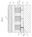
- Figure 2 is an enlarged sectional view of an ultrasonic transducer array;
- Figure 3 is an explanatory view showing a process of laying a wafer of diced piezoelectric elements on a flat layer made of a silver paste formed on a backing material;
- Figure 4 is an explanatory view showing a process of polishing and removing an upper part of the wafer which was uncuttable in the dicing process;
- Figure 5 is an explanatory view showing a process of dividing the silver paste between the piezoelectric elements by a dicing blade to separate the piezoelectric elements from one another;
- Figure 6 is an explanatory view showing a process of filling a filling material in gaps between each piezoelectric element;
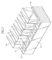
- Figure 7 is a perspective view showing an example that an insulating adhesive is used in place of the silver paste;
- Figure 8 is an enlarged sectional view showing an example that a lower part of the side face of each piezoelectric element is filled with a rigid filling material;
- Figure 9 is an enlarged sectional view showing an example that the rigid filling material is filled around a middle part of the side face of each piezoelectric element;
- Figure 10 is an enlarged sectional view showing an example that the rigid filling material is filled around an upper part of each piezoelectric element;
- Figure 11 is an enlarged sectional view showing an example that the side faces of the piezoelectric elements are connected on the central part to one another by beams;
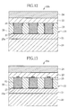
- Figure 12 is an enlarged sectional view showing an example that the side faces of the piezoelectric elements are connected on the upper part to one another by beams; and
- Figure 13 is an enlarged sectional view showing an example that the upper faces of the piezoelectric elements are connected to one another by beams.
- In Figs. 1A and 1B, an
ultrasonic transducer array 10 of convex electronic scanning type is disposed at atip 2a of anultrasonic probe 2. In theultrasonic transducer array 10, a plurality ofultrasonic transducers 11 is arranged in either one-dimensional array state as shown in Fig. 1A or two-dimensional array state as shown in Fig. 1B. In theultrasonic transducer array 10, a backing material 21 (see Fig. 2) is bonded to a curved surface of a supporting member 20 (see Fig.2) which is cylindrically formed. - An imaging device for capturing optical image of an internal body part is mounted in a
sheath 12 connected to theultrasonic transducer array 10. The imaging device includes an optical system mounted to thesheath 12 and an image sensor disposed inside thesheath 12. Thesheath 12 is provided with an exit end of a light guide for illuminating the internal body part. A channel for a wearingneedle 14 is provided at the central part of thesheath 12. Array wiring cables for electrically connecting an ultrasound observing device to theultrasonic transducer array 10, andultrasonic transducer array 10 to an endscope monitor, and an image device wiring cable for electrically connecting an endoscope monitor to the imaging device are inserted inside thesheath 12. - In Fig. 2, the
ultrasonic transducer array 10 has a structure that thebacking material 21, apiezoelectric element array 22, an acousticimpedance matching layer 23 and anacoustic lens 24 are overlaid on the supportingmember 20 in sequence on one another. - The
piezoelectric element array 22 consists ofpiezoelectric elements 25 arranged one-dimensionally or two-dimensionally and a fillingmaterial 26 filled in gaps between the adjacentpiezoelectric elements 25. Eachpiezoelectric element 25 has a thickness of, for example, 300 to 500 µm and a width of, for example, 300 µm, and an interval between eachpiezoelectric element 25 is, for example 50 µm. For example, an epoxy resin, an urethane resin, or a silicon resin is used for the fillingmaterial 26. The silicon resin may be "silicone rubber" (product name, produced by Shin-Etsu Chemical Co., Ltd.). - The
backing material 21 and thepiezoelectric elements 25 are bonded bysilver paste 27. A lower part of aside face 25a of eachpiezoelectric element 25 is surrounded by thesilver paste 27. For example, product name, "NH-050A", "NH-060A", "NH-070A" (produced by NIHON HANDA CO., LTD.) or product name,"H20S" (produced by Epoxy Technology) are used for thesilver paste 27. Thesilver paste 27 has conductivity of approximately 3.1×10⁻⁴ [Ω·cm], and preferably 10 × 10-2 to 10-4 [Ω·cm] . - The
backing material 21 consists of a flexible sheet of, for example, polyimide. Thebacking material 21 is provided with throughholes 28, which penetrate to thepiezoelectric element array 22 from the bottom of thebacking material 21. Wires 29 (approximately 80 µm in a diameter) extending from the array wiring cable are inserted in the throughholes 28, and connected to theindividual electrodes 30 of thepiezoelectric elements 25 through thesilver paste 27. - The acoustic
impedance matching layer 23 is provided for reducing a difference in acoustic impedance between thepiezoelectric elements 25 and the living body. Theacoustic lens 24 is made of, for example, a silicon resin, and overlaid on acommon electrode 31 of thepiezoelectric elements 25, such that the ultrasounds generated from theultrasonic transducer array 10 are focused to an internal body part. Theacoustic lens 24 may not be used, or a protective layer may be provided in place of theacoustic lens 24. - In manufacturing of the
ultrasonic transducer array 10, a film of thesilver paste 27 having a uniform thickness (approximately 30 µm which is 10 to 20% of the thickness of the piezoelectric elements 25) is formed on thebacking material 21 by using a squeegee, a doctor blade or a screen-printing process. A subdiced wafer of thepiezoelectric elements 25 provided with theindividual electrodes 30 is laid on the film, and thesilver paste 27 is hardened. Thereby, the lower part of theside face 25a of eachpiezoelectric element 25 is surrounded by thesilver paste 27. - Next, as shown in Fig. 4, the upper part of the wafer which was left in dicing process is grinded and removed. Subsequently, as shown in Fig. 5, the
silver paste 27 between eachpiezoelectric element 25 is cut by a dicing blade (approximately 20 µm in width) to separate thepiezoelectric elements 25 from one another. - After cutting the
silver paste 27, as shown in Fig. 6, a heat resistant tape is bonded on thepiezoelectric elements 25 and the fillingmaterials 26 are filed in the gaps between thepiezoelectric elements 25. At last, thecommon electrode 31 and the acousticimpedance matching layer 23 and the like are overlaid, and thebacking material 21 is curved to correspond to the curved surface of the supportingmember 20 then bonded to the supportingmember 20. - To capture an ultrasonic image inside a body, the
ultrasonic probe 2 is inserted into the body, and an aimed internal body part is searched whilst observing the optical image obtained by the imaging device on an endoscope monitor. When thetip 2a of theultrasonic probe 2 reaches the aimed internal part of the living body and a command to capture an ultrasonic image is entered, ultrasounds are generated from theultrasonic transducer array 10. The ultrasounds scan the living body, and echo from the living body is accordingly received by theultrasonic transducer array 10. Since the lower part of theside face 25a of eachpiezoelectric element 25 is surrounded by thesilver paste 27, the vibration of eachpiezoelectric element 25 in its width direction is restrained. - The echo from the living body is converted through the ultrasound observing device into an ultrasonic image, which is displayed on the monitor. While observing the optical image or the ultrasonic image, the wearing
needle 13 is manipulated to pick up a sample of the aimed internal body part. - As described so far, the lower part of the
side face 25a of eachpiezoelectric element 25 is surrounded by thesilver paste 27 used for bonding thepiezoelectric elements 25 to thebacking material 21, therefore the vibrations of thepiezoelectric elements 25 in the width direction can be restrained without extra manufacturing cost. Consequently, the vibration action of thepiezoelectric elements 25 in the thickness direction is stabilized and it is possible to improve acoustic characteristics of the ultrasonic transducer array. - Moreover the
piezoelectric elements 25 are tightly bonded to thebacking material 21 since eachpiezoelectric element 25 is surrounded by thesilver paste 27. Therefore, it is possible to improve workability when thebacking material 21 is curved and bonded to the curved face of the supportingmember 20, and it is also possible to enhance product reliability of theultrasonic probe 2. - In a convex electronic scanning type as described above or a radial electronic scanning type having a plurality of ultrasonic transducers concentrically arranged, when the ultrasonic transducer array is arranged on the base having curvature, the ultra transducer array is necessary to be bonded with the base plate thereof being curved backward. There is a problem that the ultrasonic transducer is peeled off from the base plate if the ultrasonic transducer is not tightly bonded to the base plate, which causes a negative effect on production yield and manufacturing cost. According to the present invention, the above problem can be easily solved owing to the above described effects.
- If the
ultrasonic transducer array 10 is one-dimensional array, an insulatingadhesive 40 may be used in place of thesilver paste 27 as shown in Fig.7. An epoxy resin, a urethane resin, or a silicon resin such as, for example, silicone rubber (product name, produced by Shin-Etsu Chemical Co.,Ltd.) may be used for the insulatingadhesive 40. In this case,conductive plates 41 made of copper and the like are attached to theindividual electrodes 30 of thepiezoelectric elements 25, and they are elongated to haveterminals 42, exposed from the insulatingadhesives 40, for connection to the array wires. - The filling
material 26 is useful for restraining vibration in a lateral direction of the piezoelectric elements 25 (in a direction perpendicular to the thickness direction). Figs 8 to 10 show embodiments of the filling material. - That is to say that, in the
ultrasonic transducer 50a in Fig. 8, the area around the lower side of theside face 25a of eachpiezoelectric element 25 surrounded by thesilver paste 27 is filled with arigid filling material 51, and the other area is filled with asoft filling material 52. In theultrasonic transducer 50b in Fig.9, an area around the middle part of the side face of eachpiezoelectric element 25 is filled with therigid filling material 51, and the other areas are filled with thesoft filling materials 52. In theultrasonic transducer 50c in Fig. 10, an area around the upper part of the side face of eachpiezoelectric element 25 is filled with therigid filling material 51, and the other areas are filled with thesoft filling material 52. Thus, the vibrations of thepiezoelectric elements 25 in the width direction can be restrained by using different types of filling materials. - Next, a filling method of the
materials ultrasonic transducer 50a in Fig.8 for instance. All the gaps between thepiezoelectric elements 25 are firstly filled up with therigid material 51. Then, therigid filling material 51 is removed by a dicing blade except for the area around the lower sides of the side faces 25a of thepiezoelectric elements 25, and thesoft filling material 52 is filled in the spaced area. It is noted that, for example an epoxy resin is used for therigid filling material 51, and a urethane resin and a silicon resin are used for thesoft filling material 52. - A table 1 shows electro mechanical coupling factors k33 of the
piezoelectric elements 25 incorporated in individualultrasonic transducers 50a, as shown in Fig. 8, each of which has different thickness ratio of the fillingmaterials materials piezoelectric elements 25 are measured at several times to calculate k33 from the obtained values of the resonance frequency Fr and anti-resonance frequency Fa. According to the table 1, k33 is 0.65 when the thickness ratio of the fillingmaterial 51 to the fillingmaterial 52 is 1:1 to 1:3, whereas k33 is 0.60 when the thickness ratio of the fillingmaterial 51 to the fillingmaterial 52 is 1: 0 (epoxy resin 100%). It is found out that the vibrations of thepiezoelectric elements 25 in the width direction are restrained if the thickness ratio is set within 1:1 to 1:3.TABLE 1 RATIO (EPOXY RESIN: URETHANE RESIN) RESONANCE FREQUENCY Fr [MHz] ANTI-RESONANCE FREQUENCY Fr [MHz] ELECTRIC MACHINE COUPLING FACTOR k33 k33 AVERAGE 1:0 - - 0.60 - 1:1 2.18 2.74 0.65 0. 65 2.14 2.72 0.66 2.15 2.69 0.64 2.11 2.73 0.68 
1:3 2.11 2.66 0.65 0.65 2.13 2.61 0.62 2.11 2.69 0.66 2.12 2.69 0.66 
- Figs 11 to 13 show
ultrasonic transducers 60a to 60c according to other embodiments of the present invention. In theultrasonic transducers 60a in Fig.11, the side faces of thepiezoelectric elements 25 are mutually connected on the central part by beams 61. In the ultrasonic transducers 60b in Fig.12, the upper part of eachpiezoelectric element 25 is connected by thebeam 61. In the ultrasonic transducers 60c in Fig.13, the upper face of eachpiezoelectric element 25 is connected by thebeam 61. If the two-dimensional array is used in theultrasonic transducers 60a to 60c, thebeams 61 are crossed in the form of parallel cross when seen from the above. - Moreover, the conductive bond material as typified by the
silver paste 27 used in the above embodiments has conductivity approximately 3.1×10⁻⁴ [Ω·cm], preferably 10×10 to 10 × 10 [Ω·cm]. However, the range of the conductivity is not limited to the above, the conductivity may be in the range of approximately 10 × 1014 [Ω·cm] at the normal temperature of 25 degrees, or the conduction-electron concentration may be in the range of 1012 [cm-3 ] to 1024 [cm-3 ]. That is to say that, a bond material made mostly of silicon, which is a semiconductor, may be used if it is conductive. - In the above embodiments, the convex electronic scanning type
ultrasonic transducer arrays ultrasonic transducer array 10 as mentioned in the above embodiments, the present invention is applicable to an actuator for driving a focusing lens or a zoom lens of a camera, and to other vibrator arrays such as a vibration-type gyroscope used in an angular velocity sensor. - Although the present invention has been fully described by the way of the preferred embodiments thereof with reference to the accompanying drawings, various changes and modifications will be apparent to those having skill in this field. Therefore, unless otherwise these changes and modifications depart from the scope of the present invention, they should be construed as included therein.
Claims (27)
- A vibrator array (10) having a base plate (21) on which a plurality of vibrators (25) is arranged in an array form, said vibrator array (10) comprising:a bond material (27) for bonding said vibrators (25) to said base plate (21), said bond material (27) surrounding lower part of a side face (25a) of each said vibrator (25).
- A vibrator array (10) as claimed in claim 1, wherein said bond material (27) has conductivity.
- A vibrator array (10) as claimed in claim 2, wherein said bond material (27) is silver paste.
- A vibrator array (10) as claimed in claim 2, wherein coating thickness of said bond material (27) is 10 to 20 % of thickness of said vibrators (25).
- A vibrator array (10) as claimed in claim 1, further comprising a filling material (26) filled in between said vibrators (25).
- A vibrator array (10) as claimed in claim 5, wherein said filling material (26) has a multilayer structure of different rigidity.
- A vibrator array (10) as claimed in claim 6, wherein hardness of a layer of said filling material (26) at the base plate side is greater than that of the other layers of said filling material.
- A vibrator array (10) as claimed in claim 6, wherein said filling material (26) has double layer, in which thickness ratio of a layer of said filling material (26) at the base plate side to the other layer of said filling material (26) is 1:1 to 1:3.
- A vibrator array (10) as claimed in claim 1, further comprising a beam member (61) for connecting said vibrators.
- A vibrator array (10) as claimed in claim 9, wherein said beam member (61) is disposed at least one of the central part of the side face (25a), the upper part of the side face (25a), and the upper face of each said vibrator (25).
- A vibrator array (10) as claimed in claim 10, further comprising a filling material (26) filled in between said vibrators (25).
- A vibrator array as claimed in claim 11, wherein said filling material has double layer, wherein thickness ratio of a layer of said filling material at the base plate side to the other layer of said filling material (26) is 1:1 to 1:3.
- A manufacturing method of a vibrator array having a base plate (21) on which a plurality of vibrators (25) is arranged in an array form, comprising steps of:subdicing a wafer to form a plurality of said vibrators (25):applying bond material (27) to said base plate (21); andbonding the bottom of each said vibrator (25) to said wafer by said bond material (27) in a manner that lower part of a side face of each said vibrator is surrounded by said bond material (27).
- A manufacturing method of a vibrator array (10) as claimed in claim 13, further comprising steps of removing an upper portion of said wafer, which connects the upper parts of said vibrators, to separate said vibrators (25).
- A manufacturing method of a vibrator array (10) as claimed in claim 14, wherein said bond material (27) has conductivity.
- A manufacturing method of a vibrator array (10) having a base plate (21) on which a plurality of vibrators (25) is arranged in an array manner, comprising steps of:subdicing a wafer to form a plurality of said vibrators (25);applying bond material (27) to said base plate (21); andbonding the bottom of each said vibrator (25) to said wafer by said bond material (27) in a manner that lower part of a side face (25a) of each said vibrator (25) is surrounded by said bond material (27).
- A manufacturing method of a vibrator array (10) as claimed in claim 16, further comprising steps of removing an upper portion of said wafer, which connects the upper parts of said vibrators (25), to separate said vibrators (25).
- A manufacturing method of a vibrator array (10) as claimed in claim 16, wherein said bond material (27) is applied to said base plate (21) in which coating thickness of said bond material is 10 to 20 % of thickness of said vibrator (25).
- A manufacturing method of a vibrator array (10) as claimed in claim 16, wherein said bond material (27) is silver paste or an insulating adhesive.
- A manufacturing method of a vibrator array (10) as claimed in claim 17, wherein a filling material (26) is further filled in between each said vibrator (25).
- A manufacturing method of a vibrator array (10) as claimed in claim 20, wherein said filling material (26) has a multilayer structure of different rigidity.
- A manufacturing method of a vibrator array (10) as claimed in claim 21, wherein hardness of a layer of said filling material at the base plate side is greater than that of the other layers of said filling material (26).
- A manufacturing method of a vibrator array (10) as claimed in claim 21, wherein said filling material (26) has double layer, wherein thickness ratio of a layer of said filling material at the base plate side to the other layer of said filling material is 1:1 to 1:3.
- A manufacturing method of a vibrator array (10) as claimed in claim 17, further comprising steps of connecting each said vibrators (25) by a beam member (61).
- An ultrasonic probe (2) comprising:a base plate (21);a plurality of vibrators (25) arranged on said base plate (21); anda bond material (27) for bonding the bottom of each said vibrator (25) to said base plate (21) in a manner to surround lower part of a side face (25a) of each said vibrator (25).
- An ultrasonic probe as claimed in claim 25, further comprising a base (20) for supporting said base plate (21), having a curved face to which said base plate (21) is attached with curvature.
- An ultrasonic probe (2) as claimed in claim 26, wherein said base (20) is any one of concave, convex and cylindrical.
Applications Claiming Priority (2)
| Application Number | Priority Date | Filing Date | Title |
|---|---|---|---|
| JP2005036438 | 2005-02-14 | ||
| JP2005339025A JP4703382B2 (en) | 2005-02-14 | 2005-11-24 | Structure of transducer array, manufacturing method thereof, and ultrasonic probe |
Publications (2)
| Publication Number | Publication Date |
|---|---|
| EP1690604A1 true EP1690604A1 (en) | 2006-08-16 |
| EP1690604B1 EP1690604B1 (en) | 2013-08-21 |
Family
ID=36124031
Family Applications (1)
| Application Number | Title | Priority Date | Filing Date |
|---|---|---|---|
| EP06002857.8A Expired - Lifetime EP1690604B1 (en) | 2005-02-14 | 2006-02-13 | Vibrator array, manufacturing method thereof and ultrasonic probe |
Country Status (3)
| Country | Link |
|---|---|
| US (2) | US7530151B2 (en) |
| EP (1) | EP1690604B1 (en) |
| JP (1) | JP4703382B2 (en) |
Cited By (2)
| Publication number | Priority date | Publication date | Assignee | Title |
|---|---|---|---|---|
| WO2010107637A2 (en) | 2009-03-18 | 2010-09-23 | Bp Corporation North America Inc. | Dry-coupled permanently installed ultrasonic sensor linear array |
| US7872949B2 (en) * | 2005-02-14 | 2011-01-18 | Fujifilm Corporation | Vibrator array, manufacturing method thereof, and ultrasonic probe |
Families Citing this family (14)
| Publication number | Priority date | Publication date | Assignee | Title |
|---|---|---|---|---|
| JP4860351B2 (en) * | 2006-05-22 | 2012-01-25 | 富士フイルム株式会社 | Curved surface attaching method and ultrasonic probe |
| JP4294678B2 (en) * | 2006-10-30 | 2009-07-15 | オリンパスメディカルシステムズ株式会社 | Ultrasonic transducer, method for manufacturing ultrasonic transducer, and ultrasonic endoscope |
| JP4544285B2 (en) * | 2007-09-28 | 2010-09-15 | 株式会社デンソー | Ultrasonic sensor |
| WO2009055767A2 (en) * | 2007-10-26 | 2009-04-30 | Trs Technologies, Inc. | Micromachined piezoelectric ultrasound transducer arrays |
| JP5399660B2 (en) * | 2008-03-13 | 2014-01-29 | 富士フイルム株式会社 | Ultrasound endoscope |
| KR101024013B1 (en) * | 2008-12-03 | 2011-03-29 | 삼성전기주식회사 | Inkjet Head Manufacturing Method |
| WO2010134243A1 (en) * | 2009-05-20 | 2010-11-25 | コニカミノルタエムジー株式会社 | Method of producing piezoelectric element array, piezoelectric element array, and ultrasonic probe |
| US8299687B2 (en) | 2010-07-21 | 2012-10-30 | Transducerworks, Llc | Ultrasonic array transducer, associated circuit and method of making the same |
| DE102010040274A1 (en) | 2010-09-06 | 2012-03-08 | Intelligendt Systems & Services Gmbh | Device for internal inspection of a workpiece having a hollow cylindrical bore |
| US20120075955A1 (en) * | 2010-09-28 | 2012-03-29 | Timothy Dean | Efficient seismic source operation in connection with a seismic survey |
| KR101386101B1 (en) | 2012-03-07 | 2014-04-16 | 삼성메디슨 주식회사 | Acoustic backing element, Transducer and Acoustic probe including the same |
| US9217797B2 (en) * | 2013-04-11 | 2015-12-22 | Schlumberger Technology Corporation | High-speed image monitoring of baseplate movement in a vibrator |
| US11090688B2 (en) | 2016-08-10 | 2021-08-17 | The Ultran Group, Inc. | Gas matrix piezoelectric ultrasound array transducer |
| CN108296154B (en) * | 2017-08-07 | 2023-12-05 | 雷索智能科技(苏州)有限公司 | Ultrasonic vibration mechanism and ultrasonic vibration device |
Citations (4)
| Publication number | Priority date | Publication date | Assignee | Title |
|---|---|---|---|---|
| US5101133A (en) | 1990-01-09 | 1992-03-31 | Richard Wolf Gmbh | Ultrasonic transducer having piezoelectric transducer elements |
| EP0524749A2 (en) * | 1991-07-10 | 1993-01-27 | Kabushiki Kaisha Toshiba | Ultrasonic probe for observing two orthogonal cross sections |
| JP2001046368A (en) | 1999-08-04 | 2001-02-20 | Olympus Optical Co Ltd | Production of ultrasonic probe |
| US6483225B1 (en) * | 2000-07-05 | 2002-11-19 | Acuson Corporation | Ultrasound transducer and method of manufacture thereof |
Family Cites Families (11)
| Publication number | Priority date | Publication date | Assignee | Title |
|---|---|---|---|---|
| US3964014A (en) * | 1974-10-15 | 1976-06-15 | General Electric Company | Sonic transducer array |
| US4122725A (en) * | 1976-06-16 | 1978-10-31 | The United States Of America As Represented By The Administrator Of The National Aeronautics And Space Administration | Length mode piezoelectric ultrasonic transducer for inspection of solid objects |
| AU529113B2 (en) * | 1978-04-19 | 1983-05-26 | Commonwealth Of Australia, The | Ultrasonic transducer array |
| JP2502685B2 (en) * | 1988-06-15 | 1996-05-29 | 松下電器産業株式会社 | Ultrasonic probe manufacturing method |
| JPH0664168A (en) * | 1992-03-11 | 1994-03-08 | Tokyo Electric Co Ltd | Ink jet printer head and manufacture thereof |
| JPH06318624A (en) * | 1993-05-07 | 1994-11-15 | Hitachi Ltd | Appearance inspection device |
| JPH0984193A (en) * | 1995-09-07 | 1997-03-28 | Denso Corp | Method for manufacturing composite piezoelectric material |
| EP1364793B1 (en) * | 2001-03-01 | 2009-07-15 | Ngk Insulators, Ltd. | Comb piezoelectric actuator, and its manufacturing method |
| JP3883822B2 (en) * | 2001-05-30 | 2007-02-21 | 日本電波工業株式会社 | Array-type ultrasonic probe |
| JP3940683B2 (en) * | 2003-02-24 | 2007-07-04 | 株式会社東芝 | Ultrasonic probe and manufacturing method thereof |
| JP4703382B2 (en) * | 2005-02-14 | 2011-06-15 | 富士フイルム株式会社 | Structure of transducer array, manufacturing method thereof, and ultrasonic probe |
-
2005
- 2005-11-24 JP JP2005339025A patent/JP4703382B2/en not_active Expired - Lifetime
-
2006
- 2006-02-13 EP EP06002857.8A patent/EP1690604B1/en not_active Expired - Lifetime
- 2006-02-14 US US11/353,138 patent/US7530151B2/en active Active
-
2008
- 2008-11-21 US US12/275,740 patent/US7872949B2/en not_active Expired - Lifetime
Patent Citations (4)
| Publication number | Priority date | Publication date | Assignee | Title |
|---|---|---|---|---|
| US5101133A (en) | 1990-01-09 | 1992-03-31 | Richard Wolf Gmbh | Ultrasonic transducer having piezoelectric transducer elements |
| EP0524749A2 (en) * | 1991-07-10 | 1993-01-27 | Kabushiki Kaisha Toshiba | Ultrasonic probe for observing two orthogonal cross sections |
| JP2001046368A (en) | 1999-08-04 | 2001-02-20 | Olympus Optical Co Ltd | Production of ultrasonic probe |
| US6483225B1 (en) * | 2000-07-05 | 2002-11-19 | Acuson Corporation | Ultrasound transducer and method of manufacture thereof |
Non-Patent Citations (1)
| Title |
|---|
| PATENT ABSTRACTS OF JAPAN vol. 2000, no. 19 5 June 2001 (2001-06-05) * |
Cited By (6)
| Publication number | Priority date | Publication date | Assignee | Title |
|---|---|---|---|---|
| US7872949B2 (en) * | 2005-02-14 | 2011-01-18 | Fujifilm Corporation | Vibrator array, manufacturing method thereof, and ultrasonic probe |
| WO2010107637A2 (en) | 2009-03-18 | 2010-09-23 | Bp Corporation North America Inc. | Dry-coupled permanently installed ultrasonic sensor linear array |
| WO2010107637A3 (en) * | 2009-03-18 | 2010-11-25 | Bp Corporation North America Inc. | Dry-coupled permanently installed ultrasonic sensor linear array |
| CN102356311A (en) * | 2009-03-18 | 2012-02-15 | Bp北美公司 | Dry-coupled permanently installed ultrasonic sensor linear array |
| US8408065B2 (en) | 2009-03-18 | 2013-04-02 | Bp Corporation North America Inc. | Dry-coupled permanently installed ultrasonic sensor linear array |
| AU2010226178B2 (en) * | 2009-03-18 | 2014-07-10 | Bp Corporation North America Inc. | Dry-coupled permanently installed ultrasonic sensor linear array |
Also Published As
| Publication number | Publication date |
|---|---|
| US20090115291A1 (en) | 2009-05-07 |
| JP4703382B2 (en) | 2011-06-15 |
| US20060181177A1 (en) | 2006-08-17 |
| EP1690604B1 (en) | 2013-08-21 |
| US7530151B2 (en) | 2009-05-12 |
| JP2006254406A (en) | 2006-09-21 |
| US7872949B2 (en) | 2011-01-18 |
Similar Documents
| Publication | Publication Date | Title |
|---|---|---|
| US7872949B2 (en) | Vibrator array, manufacturing method thereof, and ultrasonic probe | |
| US10478857B2 (en) | Piezoelectric transducers using micro-dome arrays | |
| US6640634B2 (en) | Ultrasonic probe, method of manufacturing the same and ultrasonic diagnosis apparatus | |
| US7739913B2 (en) | Joining method for curved surfaces, and ultrasonic probe and manufacturing method thereof | |
| US7288069B2 (en) | Ultrasonic probe and method of manufacturing the same | |
| EP2459322B1 (en) | Ultrasound imaging transducer acoustic stack with integral electrical connections | |
| US20080315331A1 (en) | Ultrasound system with through via interconnect structure | |
| US20110237952A1 (en) | Two-dimensional-array ultrasonic probe and ultrasonic diagnostic apparatus | |
| KR20110088384A (en) | Ultrasonic Transducer, Ultrasonic Probe, Ultrasonic Transducer Manufacturing Method | |
| JPH0723500A (en) | Two-dimensional array ultrasonic probe | |
| JP2004363746A (en) | Ultrasonic probe and its manufacturing method | |
| WO2022210887A1 (en) | Ultrasonic probe head, ultrasonic probe, and ultrasonic diagnostic apparatus | |
| JP4516451B2 (en) | Ultrasonic probe and method for producing ultrasonic probe | |
| JPH05228142A (en) | Ultrasonic probe and ultrasonic diagnostic device | |
| US12402858B2 (en) | Non-rectangular transducer arrays and associated devices, systems, and methods | |
| JP4562555B2 (en) | Ultrasonic probe and method for producing ultrasonic probe | |
| JP6543584B2 (en) | Method of manufacturing ultrasonic probe and ultrasonic diagnostic apparatus | |
| US20250072867A1 (en) | Modular acoustic sensor assemblies | |
| JP7816794B2 (en) | Flexible ultrasonic probe head, ultrasonic probe, and ultrasonic diagnostic device |
Legal Events
| Date | Code | Title | Description |
|---|---|---|---|
| PUAI | Public reference made under article 153(3) epc to a published international application that has entered the european phase |
Free format text: ORIGINAL CODE: 0009012 |
|
| AK | Designated contracting states |
Kind code of ref document: A1 Designated state(s): AT BE BG CH CY CZ DE DK EE ES FI FR GB GR HU IE IS IT LI LT LU LV MC NL PL PT RO SE SI SK TR |
|
| AX | Request for extension of the european patent |
Extension state: AL BA HR MK YU |
|
| 17P | Request for examination filed |
Effective date: 20061228 |
|
| RAP1 | Party data changed (applicant data changed or rights of an application transferred) |
Owner name: FUJIFILM CORPORATION |
|
| AKX | Designation fees paid |
Designated state(s): DE FR GB IT NL |
|
| 17Q | First examination report despatched |
Effective date: 20100322 |
|
| GRAP | Despatch of communication of intention to grant a patent |
Free format text: ORIGINAL CODE: EPIDOSNIGR1 |
|
| RIN1 | Information on inventor provided before grant (corrected) |
Inventor name: OSAWA, ATSUSHI |
|
| GRAS | Grant fee paid |
Free format text: ORIGINAL CODE: EPIDOSNIGR3 |
|
| GRAA | (expected) grant |
Free format text: ORIGINAL CODE: 0009210 |
|
| AK | Designated contracting states |
Kind code of ref document: B1 Designated state(s): DE FR GB IT NL |
|
| REG | Reference to a national code |
Ref country code: GB Ref legal event code: FG4D |
|
| REG | Reference to a national code |
Ref country code: DE Ref legal event code: R096 Ref document number: 602006037921 Country of ref document: DE Effective date: 20131017 |
|
| REG | Reference to a national code |
Ref country code: NL Ref legal event code: T3 |
|
| PLBE | No opposition filed within time limit |
Free format text: ORIGINAL CODE: 0009261 |
|
| STAA | Information on the status of an ep patent application or granted ep patent |
Free format text: STATUS: NO OPPOSITION FILED WITHIN TIME LIMIT |
|
| 26N | No opposition filed |
Effective date: 20140522 |
|
| REG | Reference to a national code |
Ref country code: DE Ref legal event code: R097 Ref document number: 602006037921 Country of ref document: DE Effective date: 20140522 |
|
| REG | Reference to a national code |
Ref country code: FR Ref legal event code: PLFP Year of fee payment: 11 |
|
| REG | Reference to a national code |
Ref country code: FR Ref legal event code: PLFP Year of fee payment: 12 |
|
| REG | Reference to a national code |
Ref country code: DE Ref legal event code: R082 Ref document number: 602006037921 Country of ref document: DE Representative=s name: KLUNKER IP PATENTANWAELTE PARTG MBB, DE |
|
| REG | Reference to a national code |
Ref country code: FR Ref legal event code: PLFP Year of fee payment: 13 |
|
| P01 | Opt-out of the competence of the unified patent court (upc) registered |
Effective date: 20230515 |
|
| PGFP | Annual fee paid to national office [announced via postgrant information from national office to epo] |
Ref country code: GB Payment date: 20241227 Year of fee payment: 20 |
|
| PGFP | Annual fee paid to national office [announced via postgrant information from national office to epo] |
Ref country code: FR Payment date: 20241231 Year of fee payment: 20 |
|
| PGFP | Annual fee paid to national office [announced via postgrant information from national office to epo] |
Ref country code: NL Payment date: 20250106 Year of fee payment: 20 |
|
| PGFP | Annual fee paid to national office [announced via postgrant information from national office to epo] |
Ref country code: DE Payment date: 20241231 Year of fee payment: 20 |
|
| PGFP | Annual fee paid to national office [announced via postgrant information from national office to epo] |
Ref country code: IT Payment date: 20250110 Year of fee payment: 20 |
|
| REG | Reference to a national code |
Ref country code: DE Ref legal event code: R071 Ref document number: 602006037921 Country of ref document: DE |
|
| REG | Reference to a national code |
Ref country code: NL Ref legal event code: MK Effective date: 20260212 |
|
| REG | Reference to a national code |
Ref country code: GB Ref legal event code: PE20 Expiry date: 20260212 |