EP1687672B1 - Fabrication of optical waveguides in periodically poled lithium niobate - Google Patents
Fabrication of optical waveguides in periodically poled lithium niobate Download PDFInfo
- Publication number
- EP1687672B1 EP1687672B1 EP04798526A EP04798526A EP1687672B1 EP 1687672 B1 EP1687672 B1 EP 1687672B1 EP 04798526 A EP04798526 A EP 04798526A EP 04798526 A EP04798526 A EP 04798526A EP 1687672 B1 EP1687672 B1 EP 1687672B1
- Authority
- EP
- European Patent Office
- Prior art keywords
- sample
- zinc
- lithium niobate
- diffusion
- waveguides
- Prior art date
- Legal status (The legal status is an assumption and is not a legal conclusion. Google has not performed a legal analysis and makes no representation as to the accuracy of the status listed.)
- Active
Links
- GQYHUHYESMUTHG-UHFFFAOYSA-N lithium niobate Chemical compound [Li+].[O-][Nb](=O)=O GQYHUHYESMUTHG-UHFFFAOYSA-N 0.000 title claims description 45
- 238000004519 manufacturing process Methods 0.000 title claims description 18
- 230000003287 optical effect Effects 0.000 title claims description 18
- 238000009792 diffusion process Methods 0.000 claims description 77
- HCHKCACWOHOZIP-UHFFFAOYSA-N Zinc Chemical compound [Zn] HCHKCACWOHOZIP-UHFFFAOYSA-N 0.000 claims description 65
- 229910052725 zinc Inorganic materials 0.000 claims description 63
- 239000011701 zinc Substances 0.000 claims description 63
- 238000000034 method Methods 0.000 claims description 46
- 230000005684 electric field Effects 0.000 claims description 20
- 239000000463 material Substances 0.000 claims description 17
- 238000010438 heat treatment Methods 0.000 claims description 9
- 239000002019 doping agent Substances 0.000 claims description 8
- 230000000737 periodic effect Effects 0.000 claims description 7
- XEEYBQQBJWHFJM-UHFFFAOYSA-N Iron Chemical compound [Fe] XEEYBQQBJWHFJM-UHFFFAOYSA-N 0.000 claims description 6
- PXHVJJICTQNCMI-UHFFFAOYSA-N Nickel Chemical compound [Ni] PXHVJJICTQNCMI-UHFFFAOYSA-N 0.000 claims description 6
- 238000001816 cooling Methods 0.000 claims description 5
- 229910052684 Cerium Inorganic materials 0.000 claims description 3
- FYYHWMGAXLPEAU-UHFFFAOYSA-N Magnesium Chemical compound [Mg] FYYHWMGAXLPEAU-UHFFFAOYSA-N 0.000 claims description 3
- GWXLDORMOJMVQZ-UHFFFAOYSA-N cerium Chemical compound [Ce] GWXLDORMOJMVQZ-UHFFFAOYSA-N 0.000 claims description 3
- 229910052742 iron Inorganic materials 0.000 claims description 3
- 229910052749 magnesium Inorganic materials 0.000 claims description 3
- 239000011777 magnesium Substances 0.000 claims description 3
- 239000000523 sample Substances 0.000 description 57
- 239000010410 layer Substances 0.000 description 26
- 229910003327 LiNbO3 Inorganic materials 0.000 description 16
- 239000010936 titanium Substances 0.000 description 13
- RTAQQCXQSZGOHL-UHFFFAOYSA-N Titanium Chemical compound [Ti] RTAQQCXQSZGOHL-UHFFFAOYSA-N 0.000 description 11
- 229910052719 titanium Inorganic materials 0.000 description 11
- 239000013078 crystal Substances 0.000 description 8
- 238000005259 measurement Methods 0.000 description 7
- 230000008569 process Effects 0.000 description 7
- 230000015572 biosynthetic process Effects 0.000 description 6
- 238000013459 approach Methods 0.000 description 5
- 230000008901 benefit Effects 0.000 description 5
- 230000000694 effects Effects 0.000 description 5
- 238000001000 micrograph Methods 0.000 description 5
- 238000000059 patterning Methods 0.000 description 4
- 229920002120 photoresistant polymer Polymers 0.000 description 4
- 239000000758 substrate Substances 0.000 description 4
- 230000008859 change Effects 0.000 description 3
- 238000012512 characterization method Methods 0.000 description 3
- 238000006243 chemical reaction Methods 0.000 description 3
- 238000000151 deposition Methods 0.000 description 3
- 239000012071 phase Substances 0.000 description 3
- 238000012545 processing Methods 0.000 description 3
- 235000012431 wafers Nutrition 0.000 description 3
- WHXSMMKQMYFTQS-UHFFFAOYSA-N Lithium Chemical compound [Li] WHXSMMKQMYFTQS-UHFFFAOYSA-N 0.000 description 2
- GRYLNZFGIOXLOG-UHFFFAOYSA-N Nitric acid Chemical compound O[N+]([O-])=O GRYLNZFGIOXLOG-UHFFFAOYSA-N 0.000 description 2
- 238000005516 engineering process Methods 0.000 description 2
- 238000002474 experimental method Methods 0.000 description 2
- 238000010348 incorporation Methods 0.000 description 2
- 238000005468 ion implantation Methods 0.000 description 2
- 150000002500 ions Chemical class 0.000 description 2
- 229910052744 lithium Inorganic materials 0.000 description 2
- 229910052759 nickel Inorganic materials 0.000 description 2
- 229910017604 nitric acid Inorganic materials 0.000 description 2
- BASFCYQUMIYNBI-UHFFFAOYSA-N platinum Chemical compound [Pt] BASFCYQUMIYNBI-UHFFFAOYSA-N 0.000 description 2
- 238000001039 wet etching Methods 0.000 description 2
- FUJCRWPEOMXPAD-UHFFFAOYSA-N Li2O Inorganic materials [Li+].[Li+].[O-2] FUJCRWPEOMXPAD-UHFFFAOYSA-N 0.000 description 1
- 230000004913 activation Effects 0.000 description 1
- 238000000137 annealing Methods 0.000 description 1
- 230000009286 beneficial effect Effects 0.000 description 1
- 230000005540 biological transmission Effects 0.000 description 1
- 239000007795 chemical reaction product Substances 0.000 description 1
- 238000012790 confirmation Methods 0.000 description 1
- 238000011109 contamination Methods 0.000 description 1
- 230000007547 defect Effects 0.000 description 1
- 230000008021 deposition Effects 0.000 description 1
- 238000005137 deposition process Methods 0.000 description 1
- 230000000994 depressogenic effect Effects 0.000 description 1
- 230000006866 deterioration Effects 0.000 description 1
- XUCJHNOBJLKZNU-UHFFFAOYSA-M dilithium;hydroxide Chemical compound [Li+].[Li+].[OH-] XUCJHNOBJLKZNU-UHFFFAOYSA-M 0.000 description 1
- 230000002349 favourable effect Effects 0.000 description 1
- 238000003384 imaging method Methods 0.000 description 1
- 230000003993 interaction Effects 0.000 description 1
- 229910052751 metal Inorganic materials 0.000 description 1
- 239000002184 metal Substances 0.000 description 1
- 238000012986 modification Methods 0.000 description 1
- 230000004048 modification Effects 0.000 description 1
- 238000000206 photolithography Methods 0.000 description 1
- 229910052697 platinum Inorganic materials 0.000 description 1
- 238000005498 polishing Methods 0.000 description 1
- 239000000047 product Substances 0.000 description 1
- 238000001228 spectrum Methods 0.000 description 1
- 230000002269 spontaneous effect Effects 0.000 description 1
- 239000002344 surface layer Substances 0.000 description 1
- 238000013519 translation Methods 0.000 description 1
- 238000011282 treatment Methods 0.000 description 1
- 230000035899 viability Effects 0.000 description 1
Images

Classifications
-
- G—PHYSICS
- G02—OPTICS
- G02F—OPTICAL DEVICES OR ARRANGEMENTS FOR THE CONTROL OF LIGHT BY MODIFICATION OF THE OPTICAL PROPERTIES OF THE MEDIA OF THE ELEMENTS INVOLVED THEREIN; NON-LINEAR OPTICS; FREQUENCY-CHANGING OF LIGHT; OPTICAL LOGIC ELEMENTS; OPTICAL ANALOGUE/DIGITAL CONVERTERS
- G02F1/00—Devices or arrangements for the control of the intensity, colour, phase, polarisation or direction of light arriving from an independent light source, e.g. switching, gating or modulating; Non-linear optics
- G02F1/35—Non-linear optics
- G02F1/355—Non-linear optics characterised by the materials used
- G02F1/3558—Poled materials, e.g. with periodic poling; Fabrication of domain inverted structures, e.g. for quasi-phase-matching [QPM]
-
- G—PHYSICS
- G02—OPTICS
- G02B—OPTICAL ELEMENTS, SYSTEMS OR APPARATUS
- G02B6/00—Light guides; Structural details of arrangements comprising light guides and other optical elements, e.g. couplings
- G02B6/10—Light guides; Structural details of arrangements comprising light guides and other optical elements, e.g. couplings of the optical waveguide type
- G02B6/12—Light guides; Structural details of arrangements comprising light guides and other optical elements, e.g. couplings of the optical waveguide type of the integrated circuit kind
- G02B2006/12083—Constructional arrangements
- G02B2006/121—Channel; buried or the like
-
- G—PHYSICS
- G02—OPTICS
- G02B—OPTICAL ELEMENTS, SYSTEMS OR APPARATUS
- G02B6/00—Light guides; Structural details of arrangements comprising light guides and other optical elements, e.g. couplings
- G02B6/10—Light guides; Structural details of arrangements comprising light guides and other optical elements, e.g. couplings of the optical waveguide type
- G02B6/12—Light guides; Structural details of arrangements comprising light guides and other optical elements, e.g. couplings of the optical waveguide type of the integrated circuit kind
- G02B2006/12083—Constructional arrangements
- G02B2006/12107—Grating
Definitions
- the present invention relates to the fabrication of optical waveguiding structures in lithium niobate.
- Quasi-phase-matched (QPM) wavelength conversion devices based on lithium niobate waveguides have been widely studied for many years.
- the main applications of this technology include telecommunication systems, nonlinear optics, and blue laser sources for next generation DVDs [1, 2, 3].
- QPM utilises periodic inversion, or poling, of the domain structure of lithium niobate to enhance the phase-matching capability of the material.
- the poled structure is commonly referred to as a grating.
- Lithium niobate poled in this way is known as periodically poled lithium niobate (PPLN).
- waveguides on PPLN substrates generally involves two steps in a sequence that depends on the choice of waveguide formation technology. For example, proton exchange involves firstly poling the lithium niobate (LiNbO 3 ) with a certain period of grating and then forming a channel waveguide, whereas titanium diffusion reverses this order.
- APE waveguides are formed at relatively low temperatures (350°C-400°C) [5, 6], so normally the waveguides are fabricated after the lithium niobate sample has been poled. Poling after the waveguide formation results in a poor periodic grating structure.
- APE waveguides show increased resistance to photorefractive damage, but support only extraordinary guided modes [5].
- proton exchanged layers decrease the nonlinear coefficient of the lithium niobate in the initial proton exchange layer [6], requiring complex post annealing to recover the nonlinearity.
- An alternative low temperature technique, ion implantation, requires the use of ion accelerators and so is complex and expensive.
- the normal temperature for titanium diffusion into LiNbO 3 is around 1050°C to 1100°C [7].
- This process is used to fabricate titanium-diffused LiNbO 3 waveguides to be used in conventional (non-QPM) optical components, such as optical modulators, which demonstrate good electro-optic properties, low propagation losses, and support both TE and TM guided modes [7].
- the diffusion process is not compatible with periodically poled materials, because at such high temperatures the periodically switched domain structure is degraded.
- the alternative sequence process of poling after the formation of waveguides has been used with some success, but the formation of an unwanted thin domain inverted layer during the high temperature process for titanium diffusion may cause problems in the subsequent poling.
- low temperature diffusion (below 1000°C) is desirable, requiring the use of elements with a high diffusion coefficient and a low activation energy.
- zinc appears to be suitable.
- the formation of low loss optical waveguides in LiNbO 3 by zinc diffusion from ZnO surface films has been demonstrated [9, 11].
- Zinc-diffused waveguides in PPLN substrates grown by the Czochralshi method have also been reported, made by zinc diffusion from the vapour phase at low temperatures [12, 13, Domenech et al (Phy. Stat. Sol. (a), vol. 192(1), pp. 135-138, 2002 )].
- Czochralshi-grown PPLN is limited in terms of quality and commercial viability, however. None of these techniques are well-developed.
- a first aspect of the present invention is directed to a method of fabricating an optical waveguide comprising the steps of: (a) providing a sample of z-cut lithium niobate having one or more gratings of periodic domain inversion defined therein by electric field poling; (b) applying a layer of metallic zinc to a z-face of the sample, the layer having a pattern corresponding to a desired pattern of optical waveguide; and (c) heating the sample in dry air to cause the zinc to diffuse into, and hence alter the refractive index of, the lithium niobate so as to form an optical waveguiding structure within the lithium niobate.
- any changes to the surface of the material caused by the diffusion can drastically change the poling characteristics later on, so that poling after diffusion can be problematic.
- a further benefit of the technique is that the metallic patterns necessary for the zinc diffusion into the lithium niobate can be precisely defined on top of the existing PPLN gratings, to give waveguides perfectly aligned with the gratings, and therefore maximum device efficiency. Typical waveguide widths are 10 ⁇ m or less, so that this high level of alignment is particularly beneficial. Hence, when the two techniques of poling narrow gratings, which can give the best grating quality, and zinc diffusion are combined, an excellent route towards high-yield device fabrication is provided.
- High quality optical structures can be obtained using the method. These have manly advantages. For example, a high resistance has been found to photorefractive damage, to which lithium niobate is particularly vulnerable. Consequently, the zinc-based waveguides are expected to allow efficient operation at room temperature and operation at blue/visible wavelengths, both of which are unattainable in devices fabricated by the existing techniques of titanium diffusion or proton exchange. Also, zinc-diffused waveguides support both TE and TM modes, a result which is unattainable via proton exchange. Further, the production efficiency of the technique can be high. The diffusion time for zinc diffusion into lithium niobate is far shorter than that for titanium diffusion or for annealed proton exchange [6,7], so that high volume production efficiency will increase accordingly.
- the method may further comprise defining the one or more gratings in the sample of lithium niobate by performing electric field poling of the sample.
- This is an alternative to using existing poled material, and can increase the flexibility of the process by allowing a user to control production from the initial virgin wafer through to the finished product, to obtain any desired structure.
- performing the electric field poling may include applying an electric field across the sample via gel electrodes applied to the +z and -z faces of the sample. While any electric field poling technique can be used, a gel electrode-based approach has been shown to give gratings that respond very well to subsequent zinc diffusion.
- the method may further comprise applying a film of metallic nickel to the z-face of the sample before applying the layer of metallic zinc, to improve adhesion of the zinc to the lithium niobate. This improves the quality of the patterning of the zinc layer, so that the waveguiding structure may be more accurately defined and positioned.
- Heating the sample may comprise heating the sample to a diffusion temperature at which the zinc diffuses into the lithium niobate, maintaining the sample at the diffusion temperature for a preselected length of time, and cooling the sample from the diffusion temperature, in which the heating and cooling are performed at a rate of substantially 6°C per minute. This rate has been found to give good results, while the diffusion temperature and length of time (diffusion time) can be selected to control the amount and extent of diffusion, and hence control the parameters of the waveguide.
- the method is not limited to pure lithium niobate.
- the lithium niobate may contain a dopant material.
- Dopants can be selected to modify material properties of the lithium niobate, such as refractive index and susceptibility to photorefractive damage.
- the dopant material may comprise one or more of iron, magnesium and cerium.
- a first approach is based on the assumption that it is possible to periodically pole the lithium niobate crystals after the zinc indiffusion process. This approach is analogous to that used in the technique of titanium diffusion in lithium niobate.
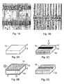
- Figures 1A and 1B show microscope images (at different magnifications) of an example result of poling a previously zinc-diffused LiNbO 3 sample.
- the domain structure of the poled sample was revealed by wet etching with diluted HF:HNO 3 solution (1:2 by volume) at room temperature.
- the period of the poling is 10 ⁇ m and the width of the waveguide is 6 ⁇ m. From these images it can be seen that the zinc-diffused area is under-poled while the remaining area is over-poled; hence the grating in the waveguide area is poor. This suggests that poling after diffusion does not give good quality results.
- Figure 2 shows a series of schematic representations illustrating various steps in the method.
- Figure 2A shows a sample 10 of lithium niobate which has been z-cut, which is to say that it is oriented with its +z and -z faces available for poling and diffusion.
- Figure 2B shows the sample 10 prepared for electric field poling.
- An array of insulating photoresist stripes 12 are patterned onto the -z face to define the periodic spacing of the poled grating.
- Electrodes 14, which may be gel electrodes, for example, are applied to both the -z and +z faces, and an electric field applied across the sample. The applied field defines the grating by causing domain inversion, giving the desired grating structure.
- Figure 2C This is depicted in Figure 2C , in which the sample 10 is shown with an array of alternately oriented domains, as indicted by the arrows.
- Figure 2C also shows the sample 10 prepared for zinc indiffusion.
- a layer 16 of metallic zinc is applied or deposited onto a z-face of the sample 10; either the +z or the -z face may be used.
- the layer is patterned in the form of a stripe in this example; this defines a pattern that corresponds to a desired shape for the eventual waveguide.
- the intended waveguide structure is a channel waveguide extending perpendicular to the grating domains.
- the sample 10 is then heated (represented by the symbol T) to a temperature high enough for zinc diffusion.
- the zinc diffuses from the surface layer 16 into the sample 10, where it alters the refractive index, so as to define an optical waveguiding structure 18.
- Figure 2D shows this end result, where the channel waveguide 18 is represented by dark shading.
- poled material for example obtained from a supplier of nonlinear crystals, can be provided as a sample into which a waveguiding structure is written or defined by zinc diffusion.
- any technique suitable for depositing and patterning the zinc layer may be used; the choice will depend in part on the suitability for defining a pattern of the shape and dimensions that match the desired waveguiding structure.
- any waveguiding structure can be fabricated using the present invention. This offers great flexibility and the ability to create a wide range of optical devices. Samples with a number of gratings can be used, for example a plurality of identical gratings or a selection of gratings with different periods. Waveguiding structures can then be fabricated in any or all of the gratings, by depositing an appropriate pattern of zinc.
- the waveguiding structure may comprise a single waveguide, several separate waveguides, or a network of connected waveguides, for example.
- a particular waveguide may extend through one or more gratings.
- Careful patterning of the zinc allows the waveguides to be precisely aligned with the gratings, for maximum efficiency of optical interactions.
- waveguides may be written in parts of the sample that do not contain gratings, since although the whole sample is heated up, the temperature required for the diffusion does not affect the grating structure.
- any pattern of waveguides can be created in a lithium niobate wafer already having any poled structure.
- the method is applicable to lithium niobate in general. Both near-stoichiometric and congruent crystals could be used, but in the near-stoichiometric case the poled gratings may not survive if the composition is too close to stoichiometry, and thus experimental confirmation of suitability will be needed before using our zinc diffusion in any given near-stoichiometric material.
- the lithium niobate can be doped with one or more dopant materials if desired or if such material is conveniently available. Dopants can be used to reduce susceptibility to photorefractive damage, to modify the refractive index, or to promote laser or amplifier activity, for example. Suitable dopants include iron, magnesium and cerium.
- a sample of z-cut 500 ⁇ m thick congruent LiNbO 3 was first cleaned in an ultrasonic bath at a temperature of 50°C. Then a thin layer of photoresist (S 1813) was spin-coated onto the -z face of the sample, upon which periodic patterns with periods A of 6.50 ⁇ m and 10 ⁇ m were defined using a Karl Suss MA4 mask aligner.
- the photoresist was then developed to leave an array of insulating stripes, and gel electrodes were applied to both z surfaces of the sample at room temperature.
- the sample was poled by using the electrodes to apply an electric field across the sample, using a computer-controlled high electric field supply device that dynamically varied the applied field in order to maintain a designated current curve.
- Q 2AP s
- A the area through which the electric field is applied
- P s the spontaneous polarisation of the sample material.
- P s 0.72 ⁇ C/mm 2 .
- the applied electric field was around 22.4 kV/mm, which is an appropriate value to cause domain reversal in LiNbO 3 .
- the time duration of the poling is proportional to the calculated charge value, which depends on the area to
- the sample was inspected under a microscope using crossed polarisers in order to check the quality of the PPLN.
- an additional consideration advantageous to the method is that of producing or using high-quality periodically poled structures in lithium niobate crystals.
- the inventors have discovered that the highest quality and highest yield PPLN gratings can be achieved when very thin periodic patterns are applied. For example, it is far simpler to fabricate a 'perfect' 10 ⁇ m-wide PPLN grating over a distance of centimetres than it is to create a 1 mm-wide grating over the same distance. This effect is likely due to avoiding as many defect sites in the crystal as possible.
- the effect also applies to the achievable periods in the sample, as the increased quality of thinner gratings allows finer periods of less than 10 ⁇ m to be readily achieved. This is more difficult in wider gratings.
- the present invention waveguides can be successfully written into or defined in these good quality yet narrow gratings, because the surface zinc layer can be applied in precise and well-defined patterns that are accurately aligned with the gratings.
- the combination of steps of the method allows high quality poled waveguides to be fabricated.
- the lithium niobate sample was thoroughly cleaned to remove any surface particulates that could cause contamination and influence the thermal diffusion process.
- zinc strips defining a desired pattern and shape of channel waveguides spaced 100 ⁇ m apart with widths varying from 1.0 ⁇ m to 7 ⁇ m and oriented parallel to the x-direction of the sample were patterned on the sample surface by photolithography.
- the -z face of the sample was used in this example. It is known that zinc atoms adhere poorly to the surface of LiNbO 3 [10], so to address this a 5-10 nm thick nickel film was deposited onto the -z face of the PPLN substrate prior to depositing the zinc layer, in order to increase adhesion of the zinc.
- the zinc film was evaporated onto the sample using a standard lift-off technique. Further samples were poled and patterned in the same way, with thicknesses of zinc varying from 80 nm to 150 nm.
- the samples were placed into a covered platinum crucible in a high-temperature oven, to undergo a thermal in-diffusion cycle.
- the cycle involved heating the samples at a rate of 6°C/min to diffusion temperature, maintaining that temperature for certain time, then cooling back down to the room temperature at rate of 6 °C/min. All the in-diffusion processing was carried out in dry air.
- Table 1 below lists the different samples (by number in the left hand column), together with the thickness of the zinc layer, and the diffusion time and temperature used for each sample: No Time (min) Zinc thickness (nm) Diffusion Temp (°C) NA-Y NA-Z Spot size-y (um) Spot size-z (um) 1 80 80 930 0.079 0.105 4.09 3.26 2 120 80 930 0.074 0.094 4.74 3.51 3 150 80 930 0.064 0.082 6.34 3.71 4 180 80 930 0.050 0.080 6.87 3.96 5 80 80 900 0.093 0.104 4.34 3.11 6 120 100 930 0.080 0.109 4.43 3.23 7 120 120 930 0.089 0.115 3.81 3.14 8 120 150 930 0.090 0.120 3.49 3.06
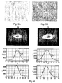
- sample No. 2 was etched in a solution of HF:HNO 3 (1:2) for ten minutes so that the structure could be viewed under a microscope.
- Figure 3A shows a microscope image of sample No. 2 after poling but before the thermal zinc diffusion of the waveguide
- Figure 3B shows a microscope image of the sample after diffusion to create a 6 ⁇ m wide zinc-diffused region in a 10 ⁇ m period grating and subsequent wet etching. Comparison of these images shows that the uniformity of the grating is preserved over the entire length of the poled sample after the diffusion. This result confirms that the periodically inverted domain structure of the PPLN substrate maintains its original form during the diffusion process. Problems of random fluctuations in domain wall position, such as occur during titanium diffusion of poled samples, are overcome.
- the end faces of the samples were cut and polished to allow optical characterisation.
- the final device length was approximately 12 mm.
- a 10x lens was used to focus the waveguide output beams onto a CCD camera mounted on a translation stage. This allowed the camera to be moved along the beam propagation direction so that the near and far field modes could be recorded.
- the camera was linked to a computer which allowed measurements to be of made parameters including beam spot size, mode profile and numerical aperture (NA) of the waveguides.
- NA numerical aperture
- Figure 4 shows measurements of the TE and TM mode profiles for channel waveguides in sample No. 2, in which the width of the metal deposited for diffusion was 2.0 ⁇ m.
- the upper images are camera images of the beam spot, with the TM mode on the left and the TE mode on the right.
- the graphs under the camera images are the corresponding profiles of the intensity I across the beam in the horizontal or y (upper graphs) and vertical or z (lower graphs) directions.
- both modes are single mode at the 633 nm wavelength, with a full width at half maximum (FWHM) mode size of 4 ⁇ m in the y direction and 2.5 ⁇ m in the z direction for the TM mode, and 4.3 ⁇ m in the y direction and 3.5 ⁇ m in the z direction for the TE mode.
- FWHM full width at half maximum
- Figure 5 shows a graph of the results of adopting the far-field technique to determine the numerical aperture (NA) the waveguide of sample No. 2.
- the graph shows measurements of the dependence of the spot size W in the y and z directions on the distance of the CCD camera to the focusing point of the beam.
- the numerical aperture is calculated from these measurements and also plotted on the graph. Larger distances lead to larger spots, which give a better estimate of the NA.
- the NA tends to be a constant figure, which, as shown, is 0.08 in the y direction and 0.11 in the z direction.
- the refractive index change ⁇ n of the waveguide of sample No. 2 has been calculated to be around 0.0015 in the y direction and 0.0025 in the z direction, achieved under the diffusion conditions listed in Table 1.
- Figure 6 shows a graph of the dependence of the FWHM spot size and the NA as a function of the diffusion time, varied from 80 min to 180 min as shown in Table 1.
- the thickness of the patterned zinc layer was 80 nm and the diffusion temperature was 930°C. The longer the diffusion time, the bigger the spot size and the smaller the NA obtained. It is observed that the spot size change in the z direction is smaller than it is in the y direction.
- Figure 7 shows a graph of the dependence of the FWHM spot size and the NA on the thickness of the zinc layer, varied from 80 nm to 150 nm as shown in Table 1.
- the diffusion temperature was 930°C and the diffusion time was 120 min.
- Figure 7 indicates that a thicker zinc film results in a smaller spot size and a larger NA.
- the thicker the zinc film the smaller the mode spot size and the better the confinement of the waveguide, hence giving a higher power intensity within the waveguide.
- the thicker zinc films resulted in a rougher sample surface due to the zinc remnant after the thermal indiffusion processing.
- Figure 8 shows a graph of the dependence of the width of single mode channel waveguides for different wavelengths on the diffusion time, at a diffusion temperature of 930°C with a zinc layer thickness of 120 nm.
- Second harmonic generation (SHG) of the output of a Nd:YAG laser at 1064 nm was then used to study the uniformity of the periodically switched domain structure inside the zinc waveguide after the thermal diffusion.
- High quality domain gratings are required for quasi-phase matched (SHG) in waveguides.
- a TM polarised incident beam was used to take advantage of the optimal non-linear susceptibility tensor coefficient of lithium niobate, the d 33 coefficient.
- An end-polished waveguide sample with a 6.5 ⁇ m grating period and a zinc waveguide of width 3.6 ⁇ m was put in a temperature-tunable oven.
- the SHG output beam was focused into an optical power meter, and the power of the SHG green light (532 nm) was measured at different temperatures.
- Figure 9 shows the results, as a plot of the variation of SHG output power with temperature. Measured data points are compared with a calculated theoretical curve. As can be seen, the QPM temperature is around 145.1°C.
- the maximum output external SHG power of 150 ⁇ W was recorded for a internal pump power of 30 mW of fundamental beam, which corresponds to a conversion efficiency of 16.7 %/Wcm 2 , with a waveguide length of 10 mm.
- the SHG measurement was carried out for 3 hours and no photorefractive damage or SHG output power fluctuations were found. This indicates that the influence of the photorefractive effect induced by generation of the second harmonic beam is depressed by the zinc diffused waveguide, compared to what would be expected for standard PPLN waveguides, such as those fabricated by proton exchange or titanium diffusion. This is highly significant, as PPLN typically suffers from photorefractive damage to the extent that usable wavelengths and powers are often limited.
Description
- The present invention relates to the fabrication of optical waveguiding structures in lithium niobate.
- Quasi-phase-matched (QPM) wavelength conversion devices based on lithium niobate waveguides have been widely studied for many years. The main applications of this technology include telecommunication systems, nonlinear optics, and blue laser sources for next generation DVDs [1, 2, 3]. QPM utilises periodic inversion, or poling, of the domain structure of lithium niobate to enhance the phase-matching capability of the material. The poled structure is commonly referred to as a grating. Lithium niobate poled in this way is known as periodically poled lithium niobate (PPLN). Several methods are now widely used for fabricating waveguides in this material, the most popular of which are annealed-proton exchange (APE) [4, 5, 6], titanium diffusion, and ion implantation. However, each of these developed techniques has some limits of applicability [7].
- The fabrication of waveguides on PPLN substrates generally involves two steps in a sequence that depends on the choice of waveguide formation technology. For example, proton exchange involves firstly poling the lithium niobate (LiNbO3) with a certain period of grating and then forming a channel waveguide, whereas titanium diffusion reverses this order. APE waveguides are formed at relatively low temperatures (350°C-400°C) [5, 6], so normally the waveguides are fabricated after the lithium niobate sample has been poled. Poling after the waveguide formation results in a poor periodic grating structure. APE waveguides show increased resistance to photorefractive damage, but support only extraordinary guided modes [5]. In addition, proton exchanged layers decrease the nonlinear coefficient of the lithium niobate in the initial proton exchange layer [6], requiring complex post annealing to recover the nonlinearity. An alternative low temperature technique, ion implantation, requires the use of ion accelerators and so is complex and expensive.
- The normal temperature for titanium diffusion into LiNbO3 is around 1050°C to 1100°C [7]. This process is used to fabricate titanium-diffused LiNbO3 waveguides to be used in conventional (non-QPM) optical components, such as optical modulators, which demonstrate good electro-optic properties, low propagation losses, and support both TE and TM guided modes [7]. However, the diffusion process is not compatible with periodically poled materials, because at such high temperatures the periodically switched domain structure is degraded. The alternative sequence process of poling after the formation of waveguides has been used with some success, but the formation of an unwanted thin domain inverted layer during the high temperature process for titanium diffusion may cause problems in the subsequent poling. An additional weakness of this technique is the worsened photorefractive damage in LiNbO3 induced by the incorporation of Ti4+ ions, which limits the operation of the Ti:LiNbO3-based devices to the infrared and visible range of the spectrum [7, 8]. Several methods for suppressing out-diffusion have been proposed, for example surface polishing off the 50 nm out-diffused layer after thermal processing [8], but those steps add complexity to the technique. In addition, it is very difficult to provide a uniform PPLN structure through a titanium in-diffused waveguide due to the electrical insulating properties of the lithium out-diffused layer in the waveguide area [7, 8].
- To overcome such difficulties, low temperature diffusion (below 1000°C) is desirable, requiring the use of elements with a high diffusion coefficient and a low activation energy. In this case, zinc appears to be suitable. The formation of low loss optical waveguides in LiNbO3 by zinc diffusion from ZnO surface films has been demonstrated [9, 11]. There is also a report on the fabrication of zinc-diffused waveguides in y-cut LiNbO3 for 1.32 µm wavelength operation by diffusion of surface metallic zinc [10]. Zinc-diffused waveguides in PPLN substrates grown by the Czochralshi method (where the PPLN domains are formed into the LiNbO3 crystal as it is grown) have also been reported, made by zinc diffusion from the vapour phase at low temperatures [12, 13, Domenech et al (Phy. Stat. Sol. (a), vol. 192(1), pp. 135-138, 2002)]. Czochralshi-grown PPLN is limited in terms of quality and commercial viability, however. None of these techniques are well-developed.
- Accordingly, a first aspect of the present invention is directed to a method of fabricating an optical waveguide comprising the steps of: (a) providing a sample of z-cut lithium niobate having one or more gratings of periodic domain inversion defined therein by electric field poling; (b) applying a layer of metallic zinc to a z-face of the sample, the layer having a pattern corresponding to a desired pattern of optical waveguide; and (c) heating the sample in dry air to cause the zinc to diffuse into, and hence alter the refractive index of, the lithium niobate so as to form an optical waveguiding structure within the lithium niobate.
- Thus, a technique is proposed in which diffusion of surface deposited metallic zinc is used to create waveguides in previously electric field-poled material. Zinc diffusion occurs at a lower temperature than titanium diffusion (930°C rather than 1050°C), which allows existing periodically poled structures and the principal nonlinear coefficient of lithium niobate, d33, to be completely preserved during diffusion. This is a huge advantage as electric field poling can be performed in virgin lithium niobate wafers using pre-optimised parameters for a high grating yield, and with no diffusion-related issues of material modification or deterioration. The ability to introduce waveguides into already poled PPLN samples allows the poling yield to be optimised before the waveguide fabrication takes place. This is important as any changes to the surface of the material caused by the diffusion, such as the incorporation of zinc or out-diffusion of lithium, can drastically change the poling characteristics later on, so that poling after diffusion can be problematic. A further benefit of the technique is that the metallic patterns necessary for the zinc diffusion into the lithium niobate can be precisely defined on top of the existing PPLN gratings, to give waveguides perfectly aligned with the gratings, and therefore maximum device efficiency. Typical waveguide widths are 10 µm or less, so that this high level of alignment is particularly beneficial. Hence, when the two techniques of poling narrow gratings, which can give the best grating quality, and zinc diffusion are combined, an excellent route towards high-yield device fabrication is provided.
- High quality optical structures can be obtained using the method. These have manly advantages. For example, a high resistance has been found to photorefractive damage, to which lithium niobate is particularly vulnerable. Consequently, the zinc-based waveguides are expected to allow efficient operation at room temperature and operation at blue/visible wavelengths, both of which are unattainable in devices fabricated by the existing techniques of titanium diffusion or proton exchange. Also, zinc-diffused waveguides support both TE and TM modes, a result which is unattainable via proton exchange. Further, the production efficiency of the technique can be high. The diffusion time for zinc diffusion into lithium niobate is far shorter than that for titanium diffusion or for annealed proton exchange [6,7], so that high volume production efficiency will increase accordingly.
- Optionally, the method may further comprise defining the one or more gratings in the sample of lithium niobate by performing electric field poling of the sample. This is an alternative to using existing poled material, and can increase the flexibility of the process by allowing a user to control production from the initial virgin wafer through to the finished product, to obtain any desired structure.
- For example, performing the electric field poling may include applying an electric field across the sample via gel electrodes applied to the +z and -z faces of the sample. While any electric field poling technique can be used, a gel electrode-based approach has been shown to give gratings that respond very well to subsequent zinc diffusion.
- Also, the method may further comprise applying a film of metallic nickel to the z-face of the sample before applying the layer of metallic zinc, to improve adhesion of the zinc to the lithium niobate. This improves the quality of the patterning of the zinc layer, so that the waveguiding structure may be more accurately defined and positioned.
- Heating the sample may comprise heating the sample to a diffusion temperature at which the zinc diffuses into the lithium niobate, maintaining the sample at the diffusion temperature for a preselected length of time, and cooling the sample from the diffusion temperature, in which the heating and cooling are performed at a rate of substantially 6°C per minute. This rate has been found to give good results, while the diffusion temperature and length of time (diffusion time) can be selected to control the amount and extent of diffusion, and hence control the parameters of the waveguide.
- The method is not limited to pure lithium niobate. The lithium niobate may contain a dopant material. Dopants can be selected to modify material properties of the lithium niobate, such as refractive index and susceptibility to photorefractive damage. For example, the dopant material may comprise one or more of iron, magnesium and cerium.
- For a better understanding of the invention and to show how the same may be carried into effect reference is now made by way of example to the accompanying drawings in which:
-
Figures 1A and 1B show microscope images of a sample of lithium niobate that has been poled by electric field poling after indiffusion of zinc; -
Figures 2A to 2D show schematic representations of a sample of lithium niobate to which steps in an embodiment of the method of the present invention are applied; -
Figures 3A and 3B show microscope images of a sample of electrically poled lithium niobate before and after formation of a zinc-diffused waveguide using an embodiment of the invention. -
Figure 4 shows measurements of TE and TM mode output beams transmitted through a zinc-diffused waveguide formed using an embodiment of the invention, as images of the beam spot and profiles of the beam intensity; -
Figure 5 shows a graph of the variation of output beam spot size and numerical aperture with distance to an imaging CCD camera for a beam transmitted through; -
Figure 6 shows a graph of the variation of output beam spot size and numerical aperture with diffusion time for zinc-diffused waveguides formed using an embodiment of the invention; -
Figure 7 shows a graph of the variation of output beam spot size and numerical aperture with thickness of deposited zinc layer for zinc-diffused waveguides formed using an embodiment of the invention; -
Figure 8 shows a graph of the variation of waveguide width with diffusion time for a range of zinc-diffused waveguides for transmission of different wavelengths formed using an embodiment of the invention; and -
Figure 9 shows a graph of the results of an experiment to measure quasi-phase matched second harmonic generation in a zinc-diffused waveguide formed using an embodiment of the invention. - In order to create a standardised route towards creating high-quality zinc-diffused waveguides in electric-field-poled PPLN crystals, two distinct fabrication routes can be considered. A first approach is based on the assumption that it is possible to periodically pole the lithium niobate crystals after the zinc indiffusion process. This approach is analogous to that used in the technique of titanium diffusion in lithium niobate.
- Therefore, attempts were made to periodically-pole high-temperature zinc-diffused LiNbO3. However, these attempts were judged to be unsuccessful owing to the presence of a thin Li2O out-diffusion induced domain-inverted layer on the +z face of the crystal, which blocks subsequent electric field poling. This is similar to the case for poling titanium-diffused LiNbO3.
-
Figures 1A and 1B show microscope images (at different magnifications) of an example result of poling a previously zinc-diffused LiNbO3 sample. The domain structure of the poled sample was revealed by wet etching with diluted HF:HNO3 solution (1:2 by volume) at room temperature. The period of the poling is 10 µm and the width of the waveguide is 6 µm. From these images it can be seen that the zinc-diffused area is under-poled while the remaining area is over-poled; hence the grating in the waveguide area is poor. This suggests that poling after diffusion does not give good quality results. - Accordingly, a method of fabricating zinc-diffused waveguides in PPLN which involves poling the sample first, and fabricating the waveguide afterwards is considered as an alternative. This approach has given highly successful results, and allows high-yield high-quality reduced photorefractive damage devices to be fabricated using a completely new process. Various fabrication conditions have been investigated and optimised to obtain waveguides for different wavelengths shown to be good quality through characterisation of mode profiles, numerical aperture (NA), spot sizes and other parameters.
-
Figure 2 shows a series of schematic representations illustrating various steps in the method.Figure 2A shows asample 10 of lithium niobate which has been z-cut, which is to say that it is oriented with its +z and -z faces available for poling and diffusion.Figure 2B shows thesample 10 prepared for electric field poling. An array of insulatingphotoresist stripes 12 are patterned onto the -z face to define the periodic spacing of the poled grating.Electrodes 14, which may be gel electrodes, for example, are applied to both the -z and +z faces, and an electric field applied across the sample. The applied field defines the grating by causing domain inversion, giving the desired grating structure. This is depicted inFigure 2C , in which thesample 10 is shown with an array of alternately oriented domains, as indicted by the arrows.Figure 2C also shows thesample 10 prepared for zinc indiffusion. Alayer 16 of metallic zinc is applied or deposited onto a z-face of thesample 10; either the +z or the -z face may be used. The layer is patterned in the form of a stripe in this example; this defines a pattern that corresponds to a desired shape for the eventual waveguide. In this case, the intended waveguide structure is a channel waveguide extending perpendicular to the grating domains. Thesample 10 is then heated (represented by the symbol T) to a temperature high enough for zinc diffusion. The zinc diffuses from thesurface layer 16 into thesample 10, where it alters the refractive index, so as to define anoptical waveguiding structure 18.Figure 2D shows this end result, where thechannel waveguide 18 is represented by dark shading. - The method as depicted in
Figure 2 is merely an example. Any electric field poling technique may be employed to fabricate the PPLN sample. However, the combination of insulating photoresist and gel electrodes has been found to give good results in combination with the zinc indiffusion. - Also, it is not necessary to perform the electric field poling as part of the method. Instead, previously poled material, for example obtained from a supplier of nonlinear crystals, can be provided as a sample into which a waveguiding structure is written or defined by zinc diffusion.
- Further, any technique suitable for depositing and patterning the zinc layer may be used; the choice will depend in part on the suitability for defining a pattern of the shape and dimensions that match the desired waveguiding structure. Within the limits of the technique selected, any waveguiding structure can be fabricated using the present invention. This offers great flexibility and the ability to create a wide range of optical devices. Samples with a number of gratings can be used, for example a plurality of identical gratings or a selection of gratings with different periods. Waveguiding structures can then be fabricated in any or all of the gratings, by depositing an appropriate pattern of zinc. This approach may be used to fabricate complex optical structures, or to make a multiplicity of individual devices (to be cut from the sample) with a single deposition and diffusion process. For a given grating, the waveguiding structure may comprise a single waveguide, several separate waveguides, or a network of connected waveguides, for example. A particular waveguide may extend through one or more gratings. Careful patterning of the zinc allows the waveguides to be precisely aligned with the gratings, for maximum efficiency of optical interactions. Alternatively or additionally, waveguides may be written in parts of the sample that do not contain gratings, since although the whole sample is heated up, the temperature required for the diffusion does not affect the grating structure. In summary, within the limits of patterning the zinc layer and poling the gratings, any pattern of waveguides can be created in a lithium niobate wafer already having any poled structure.
- The method is applicable to lithium niobate in general. Both near-stoichiometric and congruent crystals could be used, but in the near-stoichiometric case the poled gratings may not survive if the composition is too close to stoichiometry, and thus experimental confirmation of suitability will be needed before using our zinc diffusion in any given near-stoichiometric material. In either case, the lithium niobate can be doped with one or more dopant materials if desired or if such material is conveniently available. Dopants can be used to reduce susceptibility to photorefractive damage, to modify the refractive index, or to promote laser or amplifier activity, for example. Suitable dopants include iron, magnesium and cerium.
- Examples of the method of the present invention will now be described.
- In one example, a sample of z-cut 500 µm thick congruent LiNbO3 was first cleaned in an ultrasonic bath at a temperature of 50°C. Then a thin layer of photoresist (S 1813) was spin-coated onto the -z face of the sample, upon which periodic patterns with periods A of 6.50µm and 10µm were defined using a Karl Suss MA4 mask aligner.
- The photoresist was then developed to leave an array of insulating stripes, and gel electrodes were applied to both z surfaces of the sample at room temperature. After this, the sample was poled by using the electrodes to apply an electric field across the sample, using a computer-controlled high electric field supply device that dynamically varied the applied field in order to maintain a designated current curve. The poling process was terminated when a predefined charge Q had passed through the sample, where Q = 2APs; A is the area through which the electric field is applied; and Ps is the spontaneous polarisation of the sample material. For LiNbO3, Ps = 0.72 µC/mm2. The applied electric field was around 22.4 kV/mm, which is an appropriate value to cause domain reversal in LiNbO3. The time duration of the poling is proportional to the calculated charge value, which depends on the area to be poled.
- After poling, the sample was inspected under a microscope using crossed polarisers in order to check the quality of the PPLN. It should be noted that an additional consideration advantageous to the method is that of producing or using high-quality periodically poled structures in lithium niobate crystals. During experiments into the mechanics and optimisation of periodically poled materials, the inventors have discovered that the highest quality and highest yield PPLN gratings can be achieved when very thin periodic patterns are applied. For example, it is far simpler to fabricate a 'perfect' 10 µm-wide PPLN grating over a distance of centimetres than it is to create a 1 mm-wide grating over the same distance. This effect is likely due to avoiding as many defect sites in the crystal as possible. The effect also applies to the achievable periods in the sample, as the increased quality of thinner gratings allows finer periods of less than 10µm to be readily achieved. This is more difficult in wider gratings. In the case of fabricating channel waveguides in PPLN for high-efficiency second-harmonic-generation, it is often the case that such short period gratings are required. By using the present invention, waveguides can be successfully written into or defined in these good quality yet narrow gratings, because the surface zinc layer can be applied in precise and well-defined patterns that are accurately aligned with the gratings. Thus, the combination of steps of the method allows high quality poled waveguides to be fabricated.
- After poling, the lithium niobate sample was thoroughly cleaned to remove any surface particulates that could cause contamination and influence the thermal diffusion process. To prepare the sample for zinc diffusion, zinc strips defining a desired pattern and shape of channel waveguides spaced 100 µm apart with widths varying from 1.0 µm to 7 µm and oriented parallel to the x-direction of the sample were patterned on the sample surface by photolithography. The -z face of the sample was used in this example. It is known that zinc atoms adhere poorly to the surface of LiNbO3 [10], so to address this a 5-10 nm thick nickel film was deposited onto the -z face of the PPLN substrate prior to depositing the zinc layer, in order to increase adhesion of the zinc. This step may be omitted, however. Once the nickel was applied, the zinc film was evaporated onto the sample using a standard lift-off technique. Further samples were poled and patterned in the same way, with thicknesses of zinc varying from 80 nm to 150 nm.
- Then, the samples were placed into a covered platinum crucible in a high-temperature oven, to undergo a thermal in-diffusion cycle. In this example, the cycle involved heating the samples at a rate of 6°C/min to diffusion temperature, maintaining that temperature for certain time, then cooling back down to the room temperature at rate of 6 °C/min. All the in-diffusion processing was carried out in dry air.
- Table 1 below lists the different samples (by number in the left hand column), together with the thickness of the zinc layer, and the diffusion time and temperature used for each sample:
No Time (min) Zinc thickness (nm) Diffusion Temp (°C) NA-Y NA-Z Spot size-y (um) Spot size-z (um) 1 80 80 930 0.079 0.105 4.09 3.26 2 120 80 930 0.074 0.094 4.74 3.51 3 150 80 930 0.064 0.082 6.34 3.71 4 180 80 930 0.050 0.080 6.87 3.96 5 80 80 900 0.093 0.104 4.34 3.11 6 120 100 930 0.080 0.109 4.43 3.23 7 120 120 930 0.089 0.115 3.81 3.14 8 120 150 930 0.090 0.120 3.49 3.06 - In order to make sure that the gratings were still present after these high temperature treatments, sample No. 2 was etched in a solution of HF:HNO3 (1:2) for ten minutes so that the structure could be viewed under a microscope.
Figure 3A shows a microscope image of sample No. 2 after poling but before the thermal zinc diffusion of the waveguide, andFigure 3B shows a microscope image of the sample after diffusion to create a 6 µm wide zinc-diffused region in a 10 µm period grating and subsequent wet etching. Comparison of these images shows that the uniformity of the grating is preserved over the entire length of the poled sample after the diffusion. This result confirms that the periodically inverted domain structure of the PPLN substrate maintains its original form during the diffusion process. Problems of random fluctuations in domain wall position, such as occur during titanium diffusion of poled samples, are overcome. - After waveguide fabrication, the end faces of the samples were cut and polished to allow optical characterisation. The final device length was approximately 12 mm. Characterisation of the zinc-diffused channel waveguides was carried out using a He-Ne laser (λ = 632.8 nm) fibre-butt coupled into the channel waveguides. A 10x lens was used to focus the waveguide output beams onto a CCD camera mounted on a translation stage. This allowed the camera to be moved along the beam propagation direction so that the near and far field modes could be recorded. The camera was linked to a computer which allowed measurements to be of made parameters including beam spot size, mode profile and numerical aperture (NA) of the waveguides.
-
Figure 4 shows measurements of the TE and TM mode profiles for channel waveguides in sample No. 2, in which the width of the metal deposited for diffusion was 2.0 µm. The upper images are camera images of the beam spot, with the TM mode on the left and the TE mode on the right. The graphs under the camera images are the corresponding profiles of the intensity I across the beam in the horizontal or y (upper graphs) and vertical or z (lower graphs) directions. It can be seen that both modes are single mode at the 633 nm wavelength, with a full width at half maximum (FWHM) mode size of 4 µm in the y direction and 2.5 µm in the z direction for the TM mode, and 4.3 µm in the y direction and 3.5 µm in the z direction for the TE mode. Thus, the zinc-diffused waveguide supports both TM and TE modes. -
Figure 5 shows a graph of the results of adopting the far-field technique to determine the numerical aperture (NA) the waveguide of sample No. 2. The graph shows measurements of the dependence of the spot size W in the y and z directions on the distance of the CCD camera to the focusing point of the beam. The numerical aperture is calculated from these measurements and also plotted on the graph. Larger distances lead to larger spots, which give a better estimate of the NA. When the distance D is very much greater than the core size of the waveguide, the NA tends to be a constant figure, which, as shown, is 0.08 in the y direction and 0.11 in the z direction. - Based on the NA obtained in this way, the refractive index change Δn of the waveguide of sample No. 2 has been calculated to be around 0.0015 in the y direction and 0.0025 in the z direction, achieved under the diffusion conditions listed in Table 1.
- Similar measurements were made on the other samples, the results of which are listed in Table 1.
Figure 6 shows a graph of the dependence of the FWHM spot size and the NA as a function of the diffusion time, varied from 80 min to 180 min as shown in Table 1. In all cases, the thickness of the patterned zinc layer was 80 nm and the diffusion temperature was 930°C. The longer the diffusion time, the bigger the spot size and the smaller the NA obtained. It is observed that the spot size change in the z direction is smaller than it is in the y direction. -
Figure 7 shows a graph of the dependence of the FWHM spot size and the NA on the thickness of the zinc layer, varied from 80 nm to 150 nm as shown in Table 1. In all cases, the diffusion temperature was 930°C and the diffusion time was 120 min.Figure 7 indicates that a thicker zinc film results in a smaller spot size and a larger NA. Thus, the thicker the zinc film, the smaller the mode spot size and the better the confinement of the waveguide, hence giving a higher power intensity within the waveguide. However, the thicker zinc films resulted in a rougher sample surface due to the zinc remnant after the thermal indiffusion processing. This was probably caused by Zn-LiNbO3 reaction in the air, and gives a higher propagation loss owing to the scattering of light in the waveguide surface. It was also found that for a zinc film of 150 nm thickness, the remnant was far more rough than for a 120 nm film. -
Figure 8 shows a graph of the dependence of the width of single mode channel waveguides for different wavelengths on the diffusion time, at a diffusion temperature of 930°C with a zinc layer thickness of 120 nm. - From
Figures 5 to 8 , it can be seen that the fabrication of channel waveguides for different wavelengths requires different diffusion conditions. The thickness and width of the deposited zinc layer, the diffusion temperature and the diffusion time can be selected to control the characteristics of the waveguide. Samples with thicker zinc layers diffused for a shorter time are favourable for the fabrication of single mode channel waveguides with strong confinement and small spot size. Thinner zinc layers and longer diffusion times are suitable for single mode channel waveguides with smaller NA and bigger spot size. The trade-off of diffusion conditions for fabrication of single mode channel waveguides for wavelengths of 980 nm, 1064 nm and 1550 nm are listed in Table 2 below:Wavelength (nm) Thickness of Zinc layer (nm) Diffusion Time (min) Diffusion Temperature (C°) Deposited Zinc strip width (um) 980 80 80 930 3.2 1064 80 120 930 3.6 1550 120 120 930 6.4 - Second harmonic generation (SHG) of the output of a Nd:YAG laser at 1064 nm was then used to study the uniformity of the periodically switched domain structure inside the zinc waveguide after the thermal diffusion. High quality domain gratings are required for quasi-phase matched (SHG) in waveguides. A TM polarised incident beam was used to take advantage of the optimal non-linear susceptibility tensor coefficient of lithium niobate, the d33 coefficient. An end-polished waveguide sample with a 6.5 µm grating period and a zinc waveguide of width 3.6 µm (obtained using the diffusion conditions listed in Table 2) was put in a temperature-tunable oven. The SHG output beam was focused into an optical power meter, and the power of the SHG green light (532 nm) was measured at different temperatures.
Figure 9 shows the results, as a plot of the variation of SHG output power with temperature. Measured data points are compared with a calculated theoretical curve. As can be seen, the QPM temperature is around 145.1°C. The maximum output external SHG power of 150 µW was recorded for a internal pump power of 30 mW of fundamental beam, which corresponds to a conversion efficiency of 16.7 %/Wcm2, with a waveguide length of 10 mm. - The SHG measurement was carried out for 3 hours and no photorefractive damage or SHG output power fluctuations were found. This indicates that the influence of the photorefractive effect induced by generation of the second harmonic beam is depressed by the zinc diffused waveguide, compared to what would be expected for standard PPLN waveguides, such as those fabricated by proton exchange or titanium diffusion. This is highly significant, as PPLN typically suffers from photorefractive damage to the extent that usable wavelengths and powers are often limited.
- These various experimental results demonstrate the advantages and usefulness of the present invention. It provides a straightforward way of fabricating waveguides in periodically poled lithium niobate, for which there are many applications. There is flexibility in the individual steps of the method, so that these may be performed in the most convenient, efficient and appropriate manner for the desired end product. Waveguides of excellent quality and fine structure may be achieved.
-
- [1] T. Suhara, H. Ishizuki, M. Fujimura and H. Nishihara, "Waveguide Quasi-Phase-Matched Sum-Frequency Generation Device for High-Efficiency Optical Sampling", IEEE Photon. Technol. Lett. 11 .
- [2] M. H. Chou, 1. Brener, M.M. Fejer, E. E. Chanban and S. B. Christman, "1.5-µm-Band Wavelength Conversion Based on Cascaded Second-Order Nonlinearity in LiNbO3 Waveguides", IEEE Photon. Technol. Lett. 11 No. 6 June (1999) 653.
- [3] H. Kanbara, H. Itoh, M. Asobe, K. Noguchi, H. Miyazawa, T.Yanagawa and I. Yokoyama, "All-Optical Switching Based on Cascading of Second-Order Nonlinearities in a Periodically Poled Titanium-Diffused Lithium Niobate Waveguide", IEEE Photon. Technol. Lett. 11 No.3 March (1999) 328.
- [4] K. R. Parameswaran, M. Fujimura, M. H. Chou, and M. M. Fejer, "Low-Power All-Optical Gate Based on Sum Frequency Mixing in APE Waveguides in PPLN", IEEE Photon. Technol. Lett. Vol. 12, No. 6, June (2000).
- [5] Annarita Di Lallo, Alfonso Cino, Claudio Conti and Gaetano Assanto, "Second harmonic generation in reverse proton exchanged Lithium Niobate waveguides", 12 February (2001) Vol. 8, No. 2. Optic Letter Express 232.
- [6] M. L. Bortz, L. A. Eyres, and M. M. Fejer, "Depth profiling of the d33 nonlinear coefficient in annealed proton exchanged LiNbO3 waveguides," App. Phys. Lett., 62, pp. 2012-2014 (1993).
- [7] J. Amin, V. Pruneri, J. Webjorn I, P.St.J. Russell, D.C. Hanna, J.S. Wilkinson, "Blue light generation in a periodically poled Ti: Lithium Niobate channel waveguide", Optics Communications 135 (1997) 41-44.
- [8] G. Schreiber, H. Suche, Y.L.Lee, et al, "Efficient Cascaded Difference Frequency Conversion in Periodically Poled Ti: Lithium Niobate Waveguides using Pulsed and CW Pumping", Appl. Phys. B73, 501-504(2001).
- [9] W. M. Young, M. M. Fejer, M. J. F. Digonnet, A. F. Marshall, and R. S. Feigelson, J. "Fabrication, Characterization and Index Profile Modeling of High-Damage Resistance Zn-Diffused Waveguide in Congruent and MgO: Lithium Niobate", Lightwave Technol. 10, 1238, (1992).
- [10] Ruey-Ching Twu, Chia-Chih Huang, and Way-See Wang, "Zn Indiffusion Waveguide Polarizer on Y-cut LiNbO3 at 1.32-um Wavelength", IEEE Photonics Technology Letters,Vol.12, No.2, February (2000).
- [11] T. Suhara, T. Fujieda, M. Fujimura and H. Nishihara, "Fabrication Zn: Lithium Niobate Waveguides by Diffusing ZnO in Low Pressure Atmosphere", Jpn. J. Appl. Phys. 39 (2000) L864.
- [12] B.Herreros and G.Lifante, "LiNbO3 Optical Waveguides by Zn diffusion from Vapor Phase", Appl. Phys. Lett.66(12),20 March (1995).
- [13] Ruben Nevado, Eugenio Cantelar, Gines Lifante and Fernando Cusso, "Preservation of Periodically Poled Structures in Zn-Diffused Lithium Niobate Waveguides", Jpn. J. Appl. Phys. Vol.39 (2000) pp. L488-L489, .
Claims (7)
- A method of fabricating an optical waveguide comprising the steps of:(a) providing a sample of z-cut lithium niobate (10) having one or more gratings of periodic domain inversion defined therein by electric field poling;(b) applying a layer of metallic zinc (16) to a z-face of the sample (10), the layer having a pattern corresponding to a desired pattern of optical waveguide; and(c) heating the sample (10) in dry air to cause the zinc (16) to diffuse into, and hence alter the refractive index of, the lithium niobate so as to form an optical waveguiding structure (18) within the lithium niobate.
- A method according to claim 1, and further comprising defining the one or more gratings in the sample of lithium niobate (10) by performing electric field poling of the sample.
- A method according to claim 2, in which performing the electric field poling includes applying an electric field across the sample (10) via gel electrodes (14) applied to the +z and -z faces of the sample.
- A method according to any preceding claim, and further comprising applying a film of metallic nickel to the z-face of the sample (10) before applying the layer of metallic zinc (16), to improve adhesion of the zinc to the lithium niobate.
- A method according to any preceding claim, in which heating the sample (10) comprises heating the sample (10) to a diffusion temperature at which the zinc (16) diffuses into the lithium niobate, maintaining the sample (10) at the diffusion temperature for a preselected length of time, and cooling the sample (10) from the diffusion temperature, in which the heating and cooling are performed at a rate of substantially 6°C per minute.
- A method according to any preceding claim, in which the lithium niobate contains a dopant material.
- A method according to claim 6, in which the dopant material comprises one or more of iron, magnesium and cerium.
Applications Claiming Priority (3)
| Application Number | Priority Date | Filing Date | Title |
|---|---|---|---|
| GB0327267A GB0327267D0 (en) | 2003-11-24 | 2003-11-24 | Fabrication of zinc-diffused waveguides in periodically pioled lithium niobate |
| GB0405177A GB0405177D0 (en) | 2003-11-24 | 2004-03-08 | Fabrication of waveguides in lithium niobate |
| PCT/GB2004/004806 WO2005052682A1 (en) | 2003-11-24 | 2004-11-16 | Fabrication of optical waveguides in periodically poled lithium niobate |
Publications (2)
| Publication Number | Publication Date |
|---|---|
| EP1687672A1 EP1687672A1 (en) | 2006-08-09 |
| EP1687672B1 true EP1687672B1 (en) | 2013-01-02 |
Family
ID=34635442
Family Applications (1)
| Application Number | Title | Priority Date | Filing Date |
|---|---|---|---|
| EP04798526A Active EP1687672B1 (en) | 2003-11-24 | 2004-11-16 | Fabrication of optical waveguides in periodically poled lithium niobate |
Country Status (3)
| Country | Link |
|---|---|
| US (1) | US7430356B2 (en) |
| EP (1) | EP1687672B1 (en) |
| WO (1) | WO2005052682A1 (en) |
Families Citing this family (4)
| Publication number | Priority date | Publication date | Assignee | Title |
|---|---|---|---|---|
| US7649918B2 (en) * | 2007-10-30 | 2010-01-19 | Corning Incorporated | Multi-component wavelength conversion devices and lasers incorporating the same |
| CN104808289B (en) * | 2015-04-17 | 2017-11-21 | 天津理工大学 | A kind of method of the manufacturing cycle waveguide optical grating on lithium columbate crystal |
| CN106094263B (en) * | 2016-06-21 | 2018-11-13 | 天津大学 | A kind of period polarized LNOI ridge waveguides and preparation method thereof |
| GB2584877B (en) * | 2019-06-19 | 2023-02-08 | Univ Southampton | Method for fabrication of ridge waveguides |
Family Cites Families (4)
| Publication number | Priority date | Publication date | Assignee | Title |
|---|---|---|---|---|
| JP3109109B2 (en) * | 1990-07-12 | 2000-11-13 | ソニー株式会社 | Method of manufacturing optical device having periodic domain inversion structure |
| JP2750231B2 (en) * | 1990-11-05 | 1998-05-13 | 富士通株式会社 | Method of manufacturing waveguide type second harmonic generation element |
| US5875053A (en) * | 1996-01-26 | 1999-02-23 | Sdl, Inc. | Periodic electric field poled crystal waveguides |
| US7155102B2 (en) * | 2004-06-19 | 2006-12-26 | Avanex Corporation | Method and structure of electric field poling of Ti indiffused LiNbO3 substrates without the use of grinding process |
-
2004
- 2004-11-16 US US10/595,991 patent/US7430356B2/en active Active
- 2004-11-16 WO PCT/GB2004/004806 patent/WO2005052682A1/en not_active Application Discontinuation
- 2004-11-16 EP EP04798526A patent/EP1687672B1/en active Active
Non-Patent Citations (3)
| Title |
|---|
| FUJIMURA M. ET AL: "Quasi-phasemetched wavelength conversion in Zn-diffused LiNbO3 waveguides", TECHNICAL DIGEST. CLEO/PACIFIC RIM 2001. 4TH PACIFIC RIM CONFERENCE ON LASERS AND ELECTRO-OPITCS, vol. 1, no. I, 15 July 2001 (2001-07-15), CHIBA, JAPAN, pages I-96 - I-97 * |
| MAC INSTRUMENTS: "THE MAC HUMIDITY/MOISTURE HANDBOOK", 31 December 1999 (1999-12-31), Retrieved from the Internet <URL:http://www.macinstruments.com/pdf/handbook.pdf> [retrieved on 20080116] * |
| MING L. ET AL: "High conversion efficiency singly-pass second harmonic generation in a zinc-diffused periodically poled lithium niobate waveguide", OPTICS EXPRESS, vol. 13, no. 13, 27 June 2005 (2005-06-27), pages 4862 - 4868 * |
Also Published As
| Publication number | Publication date |
|---|---|
| US20070092194A1 (en) | 2007-04-26 |
| EP1687672A1 (en) | 2006-08-09 |
| US7430356B2 (en) | 2008-09-30 |
| WO2005052682A1 (en) | 2005-06-09 |
Similar Documents
| Publication | Publication Date | Title |
|---|---|---|
| EP0782017B1 (en) | Optical waveguide, optical wavelength conversion device, and methods for fabricating the same | |
| Chen | Construction of two-dimensional waveguides in insulating optical materials by means of ion beam implantation for photonic applications: fabrication methods and research progress | |
| Amin et al. | Blue light generation in a periodically poled Ti: LiNbO3 channel waveguide | |
| Ming et al. | High conversion efficiency single-pass second harmonic generation in a zinc-diffused periodically poled lithium niobate waveguide | |
| Nishida et al. | 0-dB wavelength conversion using direct-bonded QPM-Zn: LiNbO 3 ridge waveguide | |
| Roussev | Optical-frequency mixers in periodically poled lithium niobate: materials, modeling and characterization | |
| US6952307B2 (en) | Electric field poling of ferroelectric materials | |
| Risk et al. | Periodic poling and waveguide frequency doubling in RbTiOAsO4 | |
| US6926770B2 (en) | Method of fabricating two-dimensional ferroelectric nonlinear crystals with periodically inverted domains | |
| EP1687672B1 (en) | Fabrication of optical waveguides in periodically poled lithium niobate | |
| JP4579417B2 (en) | Optical waveguide manufacturing | |
| Vincent et al. | Second harmonic generation in helium-implanted periodically poled lithium niobate planar waveguides | |
| Lee et al. | Waveguide-Type Wavelength-Tunable Šolc Filter in a Periodically Poled Ti: LiNbO $ _3 $ Waveguide | |
| Pliska et al. | Linear and nonlinear optical properties of KNbO 3 ridge waveguides | |
| Feng et al. | A bond-free PPLN thin film ridge waveguide | |
| Eger et al. | Quasi-phase-matched waveguides in electric field poled, flux grown KTiOPO4 | |
| Brüske et al. | Efficient Ti: LiNbO3 ridge waveguide lasers: Investigation of Er and Yb: Er doped waveguides pumped at 980nm and 1486nm | |
| JPH04254835A (en) | Light wavelength conversion element and laser beam source utilizing the element | |
| Heinrich et al. | Waveguides in crystalline materials | |
| JP2962024B2 (en) | Method for manufacturing optical waveguide and method for manufacturing optical wavelength conversion element | |
| Jiao et al. | Optical Channel Waveguide in KTiOAsO 4 Crystals Produced by O+ ion Implantation | |
| Roussev et al. | Vapor transport equilibrated lithium niobate resistant to photorefractive damage | |
| EP1433022A2 (en) | Non-linear optical stacks | |
| Tovstonog et al. | Violet light generation in quasi-phase-matched adhered ridge waveguide | |
| JP2004045522A (en) | Manufacture method for member with optical waveguide |
Legal Events
| Date | Code | Title | Description |
|---|---|---|---|
| PUAI | Public reference made under article 153(3) epc to a published international application that has entered the european phase |
Free format text: ORIGINAL CODE: 0009012 |
|
| 17P | Request for examination filed |
Effective date: 20060511 |
|
| AK | Designated contracting states |
Kind code of ref document: A1 Designated state(s): AT BE BG CH CY CZ DE DK EE ES FI FR GB GR HU IE IS IT LI LU MC NL PL PT RO SE SI SK TR |
|
| 17Q | First examination report despatched |
Effective date: 20060904 |
|
| DAX | Request for extension of the european patent (deleted) | ||
| 17Q | First examination report despatched |
Effective date: 20060904 |
|
| APBN | Date of receipt of notice of appeal recorded |
Free format text: ORIGINAL CODE: EPIDOSNNOA2E |
|
| APBR | Date of receipt of statement of grounds of appeal recorded |
Free format text: ORIGINAL CODE: EPIDOSNNOA3E |
|
| APAF | Appeal reference modified |
Free format text: ORIGINAL CODE: EPIDOSCREFNE |
|
| APBT | Appeal procedure closed |
Free format text: ORIGINAL CODE: EPIDOSNNOA9E |
|
| GRAP | Despatch of communication of intention to grant a patent |
Free format text: ORIGINAL CODE: EPIDOSNIGR1 |
|
| RIN1 | Information on inventor provided before grant (corrected) |
Inventor name: SMITH, P.G.R. Inventor name: GAWITH, C.B.E. Inventor name: MING, L. |
|
| GRAJ | Information related to disapproval of communication of intention to grant by the applicant or resumption of examination proceedings by the epo deleted |
Free format text: ORIGINAL CODE: EPIDOSDIGR1 |
|
| GRAP | Despatch of communication of intention to grant a patent |
Free format text: ORIGINAL CODE: EPIDOSNIGR1 |
|
| GRAS | Grant fee paid |
Free format text: ORIGINAL CODE: EPIDOSNIGR3 |
|
| GRAA | (expected) grant |
Free format text: ORIGINAL CODE: 0009210 |
|
| AK | Designated contracting states |
Kind code of ref document: B1 Designated state(s): AT BE BG CH CY CZ DE DK EE ES FI FR GB GR HU IE IS IT LI LU MC NL PL PT RO SE SI SK TR |
|
| REG | Reference to a national code |
Ref country code: GB Ref legal event code: FG4D |
|
| REG | Reference to a national code |
Ref country code: CH Ref legal event code: EP Ref country code: AT Ref legal event code: REF Ref document number: 591912 Country of ref document: AT Kind code of ref document: T Effective date: 20130115 |
|
| REG | Reference to a national code |
Ref country code: IE Ref legal event code: FG4D |
|
| REG | Reference to a national code |
Ref country code: DE Ref legal event code: R096 Ref document number: 602004040665 Country of ref document: DE Effective date: 20130228 |
|
| REG | Reference to a national code |
Ref country code: AT Ref legal event code: MK05 Ref document number: 591912 Country of ref document: AT Kind code of ref document: T Effective date: 20130102 |
|
| REG | Reference to a national code |
Ref country code: NL Ref legal event code: VDEP Effective date: 20130102 |
|
| PG25 | Lapsed in a contracting state [announced via postgrant information from national office to epo] |
Ref country code: SI Free format text: LAPSE BECAUSE OF FAILURE TO SUBMIT A TRANSLATION OF THE DESCRIPTION OR TO PAY THE FEE WITHIN THE PRESCRIBED TIME-LIMIT Effective date: 20130102 |
|
| PG25 | Lapsed in a contracting state [announced via postgrant information from national office to epo] |
Ref country code: BE Free format text: LAPSE BECAUSE OF FAILURE TO SUBMIT A TRANSLATION OF THE DESCRIPTION OR TO PAY THE FEE WITHIN THE PRESCRIBED TIME-LIMIT Effective date: 20130102 Ref country code: CZ Free format text: LAPSE BECAUSE OF FAILURE TO SUBMIT A TRANSLATION OF THE DESCRIPTION OR TO PAY THE FEE WITHIN THE PRESCRIBED TIME-LIMIT Effective date: 20130102 Ref country code: IS Free format text: LAPSE BECAUSE OF FAILURE TO SUBMIT A TRANSLATION OF THE DESCRIPTION OR TO PAY THE FEE WITHIN THE PRESCRIBED TIME-LIMIT Effective date: 20130502 Ref country code: AT Free format text: LAPSE BECAUSE OF FAILURE TO SUBMIT A TRANSLATION OF THE DESCRIPTION OR TO PAY THE FEE WITHIN THE PRESCRIBED TIME-LIMIT Effective date: 20130102 Ref country code: SE Free format text: LAPSE BECAUSE OF FAILURE TO SUBMIT A TRANSLATION OF THE DESCRIPTION OR TO PAY THE FEE WITHIN THE PRESCRIBED TIME-LIMIT Effective date: 20130102 Ref country code: CY Free format text: LAPSE BECAUSE OF FAILURE TO SUBMIT A TRANSLATION OF THE DESCRIPTION OR TO PAY THE FEE WITHIN THE PRESCRIBED TIME-LIMIT Effective date: 20130102 Ref country code: ES Free format text: LAPSE BECAUSE OF FAILURE TO SUBMIT A TRANSLATION OF THE DESCRIPTION OR TO PAY THE FEE WITHIN THE PRESCRIBED TIME-LIMIT Effective date: 20130413 Ref country code: BG Free format text: LAPSE BECAUSE OF FAILURE TO SUBMIT A TRANSLATION OF THE DESCRIPTION OR TO PAY THE FEE WITHIN THE PRESCRIBED TIME-LIMIT Effective date: 20130402 |
|
| PG25 | Lapsed in a contracting state [announced via postgrant information from national office to epo] |
Ref country code: PL Free format text: LAPSE BECAUSE OF FAILURE TO SUBMIT A TRANSLATION OF THE DESCRIPTION OR TO PAY THE FEE WITHIN THE PRESCRIBED TIME-LIMIT Effective date: 20130102 Ref country code: FI Free format text: LAPSE BECAUSE OF FAILURE TO SUBMIT A TRANSLATION OF THE DESCRIPTION OR TO PAY THE FEE WITHIN THE PRESCRIBED TIME-LIMIT Effective date: 20130102 Ref country code: GR Free format text: LAPSE BECAUSE OF FAILURE TO SUBMIT A TRANSLATION OF THE DESCRIPTION OR TO PAY THE FEE WITHIN THE PRESCRIBED TIME-LIMIT Effective date: 20130403 Ref country code: PT Free format text: LAPSE BECAUSE OF FAILURE TO SUBMIT A TRANSLATION OF THE DESCRIPTION OR TO PAY THE FEE WITHIN THE PRESCRIBED TIME-LIMIT Effective date: 20130502 Ref country code: NL Free format text: LAPSE BECAUSE OF FAILURE TO SUBMIT A TRANSLATION OF THE DESCRIPTION OR TO PAY THE FEE WITHIN THE PRESCRIBED TIME-LIMIT Effective date: 20130102 |
|
| PG25 | Lapsed in a contracting state [announced via postgrant information from national office to epo] |
Ref country code: RO Free format text: LAPSE BECAUSE OF FAILURE TO SUBMIT A TRANSLATION OF THE DESCRIPTION OR TO PAY THE FEE WITHIN THE PRESCRIBED TIME-LIMIT Effective date: 20130102 Ref country code: SK Free format text: LAPSE BECAUSE OF FAILURE TO SUBMIT A TRANSLATION OF THE DESCRIPTION OR TO PAY THE FEE WITHIN THE PRESCRIBED TIME-LIMIT Effective date: 20130102 Ref country code: DK Free format text: LAPSE BECAUSE OF FAILURE TO SUBMIT A TRANSLATION OF THE DESCRIPTION OR TO PAY THE FEE WITHIN THE PRESCRIBED TIME-LIMIT Effective date: 20130102 Ref country code: EE Free format text: LAPSE BECAUSE OF FAILURE TO SUBMIT A TRANSLATION OF THE DESCRIPTION OR TO PAY THE FEE WITHIN THE PRESCRIBED TIME-LIMIT Effective date: 20130102 |
|
| PLBE | No opposition filed within time limit |
Free format text: ORIGINAL CODE: 0009261 |
|
| STAA | Information on the status of an ep patent application or granted ep patent |
Free format text: STATUS: NO OPPOSITION FILED WITHIN TIME LIMIT |
|
| 26N | No opposition filed |
Effective date: 20131003 |
|
| PG25 | Lapsed in a contracting state [announced via postgrant information from national office to epo] |
Ref country code: IT Free format text: LAPSE BECAUSE OF FAILURE TO SUBMIT A TRANSLATION OF THE DESCRIPTION OR TO PAY THE FEE WITHIN THE PRESCRIBED TIME-LIMIT Effective date: 20130102 |
|
| REG | Reference to a national code |
Ref country code: DE Ref legal event code: R097 Ref document number: 602004040665 Country of ref document: DE Effective date: 20131003 |
|
| REG | Reference to a national code |
Ref country code: CH Ref legal event code: PL |
|
| PG25 | Lapsed in a contracting state [announced via postgrant information from national office to epo] |
Ref country code: LI Free format text: LAPSE BECAUSE OF NON-PAYMENT OF DUE FEES Effective date: 20131130 Ref country code: CH Free format text: LAPSE BECAUSE OF NON-PAYMENT OF DUE FEES Effective date: 20131130 Ref country code: MC Free format text: LAPSE BECAUSE OF FAILURE TO SUBMIT A TRANSLATION OF THE DESCRIPTION OR TO PAY THE FEE WITHIN THE PRESCRIBED TIME-LIMIT Effective date: 20130102 |
|
| REG | Reference to a national code |
Ref country code: IE Ref legal event code: MM4A |
|
| PG25 | Lapsed in a contracting state [announced via postgrant information from national office to epo] |
Ref country code: IE Free format text: LAPSE BECAUSE OF NON-PAYMENT OF DUE FEES Effective date: 20131116 |
|
| PG25 | Lapsed in a contracting state [announced via postgrant information from national office to epo] |
Ref country code: TR Free format text: LAPSE BECAUSE OF FAILURE TO SUBMIT A TRANSLATION OF THE DESCRIPTION OR TO PAY THE FEE WITHIN THE PRESCRIBED TIME-LIMIT Effective date: 20130102 |
|
| PG25 | Lapsed in a contracting state [announced via postgrant information from national office to epo] |
Ref country code: HU Free format text: LAPSE BECAUSE OF FAILURE TO SUBMIT A TRANSLATION OF THE DESCRIPTION OR TO PAY THE FEE WITHIN THE PRESCRIBED TIME-LIMIT; INVALID AB INITIO Effective date: 20041116 Ref country code: LU Free format text: LAPSE BECAUSE OF NON-PAYMENT OF DUE FEES Effective date: 20131116 |
|
| REG | Reference to a national code |
Ref country code: FR Ref legal event code: PLFP Year of fee payment: 12 |
|
| REG | Reference to a national code |
Ref country code: FR Ref legal event code: PLFP Year of fee payment: 13 |
|
| REG | Reference to a national code |
Ref country code: FR Ref legal event code: PLFP Year of fee payment: 14 |
|
| REG | Reference to a national code |
Ref country code: DE Ref legal event code: R082 Ref document number: 602004040665 Country of ref document: DE Representative=s name: D YOUNG & CO LLP, DE |
|
| PGFP | Annual fee paid to national office [announced via postgrant information from national office to epo] |
Ref country code: GB Payment date: 20231123 Year of fee payment: 20 |
|
| PGFP | Annual fee paid to national office [announced via postgrant information from national office to epo] |
Ref country code: FR Payment date: 20231120 Year of fee payment: 20 Ref country code: DE Payment date: 20231121 Year of fee payment: 20 |