EP1684306A2 - Phase change memory device and data writing method - Google Patents
Phase change memory device and data writing method Download PDFInfo
- Publication number
- EP1684306A2 EP1684306A2 EP06001272A EP06001272A EP1684306A2 EP 1684306 A2 EP1684306 A2 EP 1684306A2 EP 06001272 A EP06001272 A EP 06001272A EP 06001272 A EP06001272 A EP 06001272A EP 1684306 A2 EP1684306 A2 EP 1684306A2
- Authority
- EP
- European Patent Office
- Prior art keywords
- lines
- voltage
- line
- memory device
- semiconductor memory
- Prior art date
- Legal status (The legal status is an assumption and is not a legal conclusion. Google has not performed a legal analysis and makes no representation as to the accuracy of the status listed.)
- Granted
Links
Images



Classifications
-
- G—PHYSICS
- G11—INFORMATION STORAGE
- G11C—STATIC STORES
- G11C13/00—Digital stores characterised by the use of storage elements not covered by groups G11C11/00, G11C23/00, or G11C25/00
- G11C13/0002—Digital stores characterised by the use of storage elements not covered by groups G11C11/00, G11C23/00, or G11C25/00 using resistive RAM [RRAM] elements
- G11C13/0004—Digital stores characterised by the use of storage elements not covered by groups G11C11/00, G11C23/00, or G11C25/00 using resistive RAM [RRAM] elements comprising amorphous/crystalline phase transition cells
-
- E—FIXED CONSTRUCTIONS
- E04—BUILDING
- E04B—GENERAL BUILDING CONSTRUCTIONS; WALLS, e.g. PARTITIONS; ROOFS; FLOORS; CEILINGS; INSULATION OR OTHER PROTECTION OF BUILDINGS
- E04B1/00—Constructions in general; Structures which are not restricted either to walls, e.g. partitions, or floors or ceilings or roofs
- E04B1/18—Structures comprising elongated load-supporting parts, e.g. columns, girders, skeletons
- E04B1/24—Structures comprising elongated load-supporting parts, e.g. columns, girders, skeletons the supporting parts consisting of metal
-
- E—FIXED CONSTRUCTIONS
- E04—BUILDING
- E04C—STRUCTURAL ELEMENTS; BUILDING MATERIALS
- E04C3/00—Structural elongated elements designed for load-supporting
- E04C3/02—Joists; Girders, trusses, or trusslike structures, e.g. prefabricated; Lintels; Transoms; Braces
- E04C3/04—Joists; Girders, trusses, or trusslike structures, e.g. prefabricated; Lintels; Transoms; Braces of metal
-
- G—PHYSICS
- G11—INFORMATION STORAGE
- G11C—STATIC STORES
- G11C11/00—Digital stores characterised by the use of particular electric or magnetic storage elements; Storage elements therefor
- G11C11/56—Digital stores characterised by the use of particular electric or magnetic storage elements; Storage elements therefor using storage elements with more than two stable states represented by steps, e.g. of voltage, current, phase, frequency
- G11C11/5678—Digital stores characterised by the use of particular electric or magnetic storage elements; Storage elements therefor using storage elements with more than two stable states represented by steps, e.g. of voltage, current, phase, frequency using amorphous/crystalline phase transition storage elements
-
- G—PHYSICS
- G11—INFORMATION STORAGE
- G11C—STATIC STORES
- G11C13/00—Digital stores characterised by the use of storage elements not covered by groups G11C11/00, G11C23/00, or G11C25/00
- G11C13/0002—Digital stores characterised by the use of storage elements not covered by groups G11C11/00, G11C23/00, or G11C25/00 using resistive RAM [RRAM] elements
- G11C13/0021—Auxiliary circuits
- G11C13/004—Reading or sensing circuits or methods
-
- G—PHYSICS
- G11—INFORMATION STORAGE
- G11C—STATIC STORES
- G11C13/00—Digital stores characterised by the use of storage elements not covered by groups G11C11/00, G11C23/00, or G11C25/00
- G11C13/0002—Digital stores characterised by the use of storage elements not covered by groups G11C11/00, G11C23/00, or G11C25/00 using resistive RAM [RRAM] elements
- G11C13/0021—Auxiliary circuits
- G11C13/0069—Writing or programming circuits or methods
-
- E—FIXED CONSTRUCTIONS
- E04—BUILDING
- E04C—STRUCTURAL ELEMENTS; BUILDING MATERIALS
- E04C3/00—Structural elongated elements designed for load-supporting
- E04C3/02—Joists; Girders, trusses, or trusslike structures, e.g. prefabricated; Lintels; Transoms; Braces
- E04C3/04—Joists; Girders, trusses, or trusslike structures, e.g. prefabricated; Lintels; Transoms; Braces of metal
- E04C2003/0404—Joists; Girders, trusses, or trusslike structures, e.g. prefabricated; Lintels; Transoms; Braces of metal beams, girders, or joists characterised by cross-sectional aspects
- E04C2003/0443—Joists; Girders, trusses, or trusslike structures, e.g. prefabricated; Lintels; Transoms; Braces of metal beams, girders, or joists characterised by cross-sectional aspects characterised by substantial shape of the cross-section
- E04C2003/0447—Joists; Girders, trusses, or trusslike structures, e.g. prefabricated; Lintels; Transoms; Braces of metal beams, girders, or joists characterised by cross-sectional aspects characterised by substantial shape of the cross-section circular- or oval-shaped
-
- G—PHYSICS
- G11—INFORMATION STORAGE
- G11C—STATIC STORES
- G11C13/00—Digital stores characterised by the use of storage elements not covered by groups G11C11/00, G11C23/00, or G11C25/00
- G11C13/0002—Digital stores characterised by the use of storage elements not covered by groups G11C11/00, G11C23/00, or G11C25/00 using resistive RAM [RRAM] elements
- G11C13/0021—Auxiliary circuits
- G11C13/0069—Writing or programming circuits or methods
- G11C2013/009—Write using potential difference applied between cell electrodes
-
- G—PHYSICS
- G11—INFORMATION STORAGE
- G11C—STATIC STORES
- G11C2213/00—Indexing scheme relating to G11C13/00 for features not covered by this group
- G11C2213/70—Resistive array aspects
- G11C2213/72—Array wherein the access device being a diode
Definitions
- the invention relates to a semiconductor memory device and a data writing method.
- This application claims priority to Korean Patent Application No. 10-2005-0006581, filed on January 25, 2005, the disclosure of which is incorporated by reference herein in its entirety.
- Phase change random access memories are nonvolatile memory devices which store data using a phase change material, e.g., Ge-Sb-Te (GST), whose resistance changes in accordance with a phase transition due to a change in temperature.
- a phase change material e.g., Ge-Sb-Te (GST)
- GST Ge-Sb-Te
- FIG. 1 illustrates an equivalent circuit of a unit cell C of a PRAM.
- the unit cell C consists of a P-N diode D and a phase change material GST.
- the phase change material GST is connected to a bit line BL and a P-junction of the diode D.
- a word line WL is connected to an N-junction of the diode D.
- the phase change material GST of the PRAM unit cell C goes into a crystalline state or an amorphous state depending on a temperature applied thereto and a heating time. This enables data to be stored in the PRAM cell.
- a temperature higher than 900°C is needed for a phase transition of the phase change material GST.
- Such temperatures are obtained by Joule heating which uses a current flowing through the PRAM cell to increase or decrease the temperature thereof.
- phase change material GST is heated above its melting temperature by a current and then it is rapidly cooled.
- the phase change material GST then goes into the amorphous state and stores a data "1 ". This state is referred to as a reset state.
- the phase change material GST is then heated above its crystallization temperature for a predetermined period of time and cooled.
- the phase change material GST goes into the crystalline state and stores a data "0". This state is referred to as a set state.
- phase change material GST A read operation for the phase change material GST will now be described. After a bit line and a word line are used to select a memory cell, an external current is provided to the selected memory cell. It is then determined whether data to be stored in the selected memory cell is "1" or "0" based on a change in voltage according to a resistance value of the phase change material GST of the selected memory cell.
- FIG. 2 illustrates a semiconductor memory device 200 comprising a memory cell array MAY including a plurality of the PRAM unit cells C shown in FIG. 1.
- An exemplary structure of the memory cell array MAY is disclosed in the patent publications US 6,667,900 and US 6,567,296.
- the semiconductor memory device 200 comprises the memory cell array MAY and a word line driver 210.
- the memory cell array MAY comprises a plurality of unit cells C connected to corresponding bit lines BL0 ⁇ BLk-1 and word lines WL0, WL1, and WL2. Although only k bit lines BL0 ⁇ BLk-1 and three word lines WL0, WL1, and WL2 are shown in FIG. 2, the number of bit lines and word lines is not limited thereto.
- the word line driver 210 selects one of the word lines WL0, WL1, and WL2. The selected word line is then set to a low level. If a first bit line BL0 and a first word line WL0 are sequentially selected, a write current applied to the first bit line BL0 flows through a unit cell connected between the first bit line BL0 and the first word line WL0. The state of the phase change material of the unit cell is then changed to store data.
- Each of the word lines WL0, WL1, and WL2 has its own resistance R_WL. Since the word lines WL0, WL1, and WL2 pass current when writing data, the resistance R_WL should be minimized. However, since the word lines WL0, WL1, and WL2 have a high resistance, the number of unit cells connected to the word lines WL0, WL1, and WL2 is limited. Further, the word line driver 210 should be powerful enough to drive the word lines WL0, WL1, and WL2.
- the write current is applied to the first bit line BL0, and the first word line WL0 is set to a low level by the word line driver 210.
- the second and third word lines WL1 and WL2 are then in a floating state.
- the first bit line BL0 maintains a relatively high voltage due to the applied write current
- the second and third word lines WL1 and WL2 maintain a relatively low level in the floating state. Therefore, current flows through unit cells connected between the first word line WLO and the second and third word lines WL1 and WL2, which can change the state of the phase change material in those unit cells.
- the invention solves this problem by providing a semiconductor memory device having the features of claim 1 and a data writing method having the features of claim 12.
- Advantageous embodiments of the invention are mentioned in the subclaims, the wording of which is herewith incorporated into the specification by reference to avoid unnecessary text repetition.
- a semiconductor memory device and a data writing method are provided that prevent current from flowing from a selected bit line to a non-selected word line by maintaining a constant voltage in the non-selected word line, thereby enabling stable sensing and increasing the operating speed of the semiconductor memory device.
- a semiconductor memory device comprising: a memory cell array including a plurality of memory cells in which a first terminal of a memory cell is connected to a corresponding first line among a plurality of first lines and a second terminal of a memory cell is connected to a corresponding second line among a plurality of second lines; and bias circuits for biasing a selected second line among the second lines to a first voltage and a non-selected second line to a second voltage.
- the first voltage may be a ground voltage and the second voltage may be a power voltage.
- the bias circuits may comprise: NMOS transistors connected between the second lines and the ground voltage; and PMOS transistors connected between the second lines and the power voltage.
- Drains of the NMOS transistors may be connected to the second lines, sources are connected to the ground voltage, and main word line signals are applied to gates of the NMOS transistors; and drains of the PMOS transistors are connected to the second lines, sources are connected to the power voltage, and the main word line signals are applied to gates of the PMOS transistors.
- the semiconductor memory device may further comprise a word line driver which generates the main word line signals in response to a word line enable signal and a block address.
- the semiconductor memory device may further comprise diode transistors connected between the power voltage and the PMOS transistors.
- the second voltage may be obtained by subtracting a threshold voltage of the diode transistors from the power voltage.
- the bias circuits may comprise inverters for biasing the selected second line to the first voltage in response to the main word line signals.
- the semiconductor memory device may further comprise: a word line driver which generates the main word line signals in response to a word line enable signal and a block address.
- Each memory cell may comprise: a phase change material connected to one of the first lines; and a diode connected between the phase change material and one of the second lines.
- a method of writing data to a selected memory cell connected to a selected first line and a selected second line of a semiconductor memory device including a plurality of memory cells in which a first terminal of a memory cell is connected to a corresponding first line among a plurality of first lines and a second terminal of a memory cell is connected to a corresponding second line among a plurality of second lines, the method comprising: biasing the selected first line to a predetermined voltage; biasing the selected second line to a first voltage; and basing non-selected second lines to a second voltage.
- a semiconductor memory device comprising: a plurality of first lines and a plurality of second lines; and a memory cell array including a plurality of memory cells in which a first terminal of a memory cell is connected to a corresponding one of the first lines and a second terminal of the memory cell is connected to a corresponding one of the second lines; wherein a selected second line is biased to a first voltage; and non-selected second lines are biased to a second voltage.
- the semiconductor memory device may further comprise bias circuits which control the voltage of the second lines; wherein the bias circuits comprise: NMOS transistors which bias the selected second line to the first voltage; and PMOS transistors which bias non-selected second lines to the second voltage.
- a semiconductor memory device comprising: a memory cell array including a plurality of phase change memory cells in which a first terminal of a phase change memory cell is connected to a corresponding first line among a plurality of first lines and a second terminal of a phase change memory cell is connected to a corresponding second line among a plurality of second lines; and inverters for biasing a selected second line to a first voltage and non-selected second lines to a second voltage in response to main word line signals.
- Input terminals of the inverters may receive the main word line signals, and output terminals of the inverters are connected to the second lines.
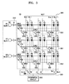
- FIG. 3 illustrates a semiconductor memory device 300 according to an embodiment of the invention which includes a memory cell array MAY, bias circuits BS0, BS1, and BS2, and a word line driver 310.
- the semiconductor memory device 300 is a PRAM, which includes a memory cell having a phase change material, e.g., GST, connected to a first line, and a diode connected between the phase change material and a second line.
- the PRAM may be similar to or the same as that shown in FIG. 1.
- the semiconductor memory device 300 is connected to a peripheral circuit 330 and a column decoder 320.
- the peripheral circuit 330 may comprise a write driver (not shown) and a sense amplification circuit (not shown).
- the column decoder 320 includes transistors TR0, TR1, ⁇ TRn-1 which are turned on or off in response to column selection signals Y0 ⁇ Yn-1.
- the memory cell array MAY includes a plurality of memory cells in which a first terminal of a memory cell is connected to a corresponding first line among a plurality of n first lines BL0 ⁇ BLn-1 where n is a natural number, and a second terminal of the memory cell is connected to a corresponding second line among a plurality of second lines LWL0, LWL1, and LWL2.
- the plurality of first lines BL0 ⁇ BLn-1 are bit lines and the plurality of second lines LWL0, LWL1, and LWL2 are word lines. Even though only three second lines LWL0, LWL1, and LWL2 are shown in FIG. 3, the number of second lines is not limited thereto.
- the bias circuits BS0, BS1, and BS2 bias a selected second line to a first voltage and a non-selected second line to a second voltage.
- the first voltage is a ground voltage and the second voltage is a power voltage VDD.
- selected means that the corresponding second line is activated by the word line driver 310 to write data to the memory cell connected to the second line.
- the semiconductor memory device 300 maintains the voltage of a selected word line at the ground voltage, and prevents non-selected word lines from floating, thereby preventing a current from flowing from a selected bit line to the non-selected word line. In this way, the semiconductor memory device 300 can perform stable sensing, and increase its operating speed.
- the bias circuits BS0, BS1, and BS2 comprise NMOS transistors NTR01 ⁇ NTR23 connected between each of the second lines LWL0, LWL1, and LWL2 and a ground voltage VSS, and PMOS transistors PTR0, PTR1, PTR2 connected between each of the second lines LWL0, LWL1, and LWL2 and the power voltage VDD.
- the number of NMOS transistors is not limited thereto.
- the number of NMOS transistors can vary according to the number of memory cells connected to the second lines LWL0, LWL1, and LWL2 and the length of the second lines LWL0, LWL1, and LWL2.
- the drains of the NMOS transistors NTR01 ⁇ NTR23 are connected to the second lines LWL0, LWL1, and LWL2, and the sources are connected to the ground voltage VSS, and main word line signals SWL0, SWL1, and SWL2 are applied to the gates of the NMOS transistors NTR01 -NTR23.
- the word line driver 310 generates the main word line signals SWL0, SWL1, and SWL2 in response to word line enable signals X0, X1, and X2 and block addresses BLK0, BLK1, and BLK2.
- a main word line signal corresponding to a selected second line has a high level
- a main word line signal corresponding to a non-selected second line has a low level.
- a write current is applied to a first bit line BL0.
- Data is then written to a memory cell connected between the first bit line BL0 and a first word line LWL0 (which may be a local word line).
- a NAND gate N0 and an inverter I0 generate the first main word line signal SWL0 at a high level.
- the first main word line signal SWL0 is then generated at a high level and the other main word line signals SLW1 and SWL2 are generated at a low level to select the first word line LWL0.
- the NMOS transistors NTR01 ⁇ NTR23 of the first bias circuit BS0 are turned on in response to the high level of the first main word line signal SWL0, and the first word line LWL0 goes to a low level.
- the PMOS transistor PTR0 of the first bias circuit BS0 is turned off.
- the write current applied to the first bit line BL0 flows to ground through a memory cell and the first word line LWL0 so that data is stored in the memory cell.
- the PMOS transistors PTR1 and PTR2 of the second and third bias circuits BS1 and BS2 are turned on by the second and third main word line signals SWL1 and SWL2 at a low level, and the voltage of the second and third word lines LWL1 and LWL2 becomes the power voltage VDD.
- the write current applied to the first bit line BL0 does not flow to the second and third word lines LWL1 and LWL2 since the second and third word lines LWL1 and LWL2 are at the power voltage VDD.
- memory cells other than that connected to the first bit line BL0 and the first word line LWL0 can stably hold data since they are not influenced by the write current of the first bit line BLO.
- FIG. 4 illustrates a semiconductor memory device 400 according to another embodiment of the invention.
- the semiconductor memory device 400 has the same or similar structure and operation as the semiconductor memory device 300 shown in FIG. 3. However, the structure of bias circuits BS0, BS1, and BS2 of the semiconductor memory device 400 is different than that of the bias circuits BS0, BS1, and BS2 of the semiconductor memory device 300.
- the bias circuits BS0, BS1, and BS2 of the semiconductor memory device 400 include diode transistors DTR0, DTR1, and DTR2 connected between the power voltage VDD and the sources of the PMOS transistors PTR0, PTR1, and PTR2.
- Word lines e.g., the second and third word lines LWL1 and LWL2 which are not selected by the diode transistors DTR0, DTR1, and DTR2 are at a voltage obtained by subtracting the threshold voltage of the diode transistors DTR0, DTR1, and DTR2 from the power voltage VDD.
- the voltage applied to a bit line to create the write current is lower than the power voltage VDD and non-selected word lines maintain a voltage lower than the power voltage VDD.
- FIG. 5 illustrates still another semiconductor memory device 500 according to an embodiment of the invention.
- the semiconductor memory device 500 has the same or similar structure as the semiconductor memory device 300 shown in FIG. 3. However, the structure of bias circuits BS0, BS1, and BS2 of the semiconductor memory device 500 is different than that of the bias circuits BS0, BS1, and BS2 of the semiconductor memory device 300.
- the bias circuits BS0, BS1, and BS2 of the semiconductor memory device 500 include inverters I01 ⁇ I23 for biasing a selected second line to a first voltage in response to the main word line signals SWL0, SWL1, and SWL2.
- the inverters I01 ⁇ I23 perform the functions of the NMOS transistors NTR01 ⁇ NTR23 and the PMOS transistors PTR0, PTR1, PTR2 included in the bias circuits BS0, BS1, and BS2 shown in FIG. 3.
- the main word line signal SWL0 is generated at a high level
- other main word line signals SWL1 and SWL2 are generated at a low level.
- the inverters I01, 102, and I03 of the first bias circuit BSO invert the voltage of the first word line LWL0 to a low level.
- the inverters I11 ⁇ I23 of the second and third bias circuits BS1 and BS2 invert the voltage of the second and third word lines LWL2 and LWL3 to a high level.
- the bias circuits BS0, BS1, and BS2 of the semiconductor memory device 500 perform the same or similar function as the bias circuits BS0, BS1, and BS2 of the semiconductor memory device 300.
- the data writing method may be used by one of the semiconductor memory devices 300, 400 or 500.
- the data writing method may be used by a semiconductor memory device other than the semiconductor memory devices 300, 400 or 500 that includes a plurality of memory cells, in which a first terminal of a memory cell is connected to a corresponding first line among a plurality of first lines, and a second terminal connected to a corresponding second line among a plurality of second lines.
- data is written to a selected memory cell connected to a selected first line and a selelcted second line of a semiconductor memory device.
- the selected first line is biased to a predetermined voltage and the first line is a bit line and the selected first line is a bit line connected to a memory cell for applying data.
- a write current for writing data is then applied to a bit line and the selected second line is biased to a first voltage.
- the selected second line is a word line connected to a memory cell for writing data.
- the first voltage lowers the voltage of the word line connected to the memory cell for writing data.
- Non-selected second lines are biased to a second voltage and the non-selected second lines are word lines other than the word line connected to the memory cell for writing data.
- the second voltage lowers the voltage of non-selected second lines other than the word line connected to the memory cell for writing data. In this way, a current is prevented from flowing from a selected bit line to a non-selected word line.
Landscapes
- Engineering & Computer Science (AREA)
- Architecture (AREA)
- Chemical & Material Sciences (AREA)
- Crystallography & Structural Chemistry (AREA)
- Civil Engineering (AREA)
- Structural Engineering (AREA)
- Computer Hardware Design (AREA)
- Physics & Mathematics (AREA)
- Electromagnetism (AREA)
- Static Random-Access Memory (AREA)
- Read Only Memory (AREA)
- Semiconductor Memories (AREA)
Abstract
Description
- The invention relates to a semiconductor memory device and a data writing method. This application claims priority to Korean Patent Application No. 10-2005-0006581, filed on January 25, 2005, the disclosure of which is incorporated by reference herein in its entirety.
- Phase change random access memories (PRAMs) are nonvolatile memory devices which store data using a phase change material, e.g., Ge-Sb-Te (GST), whose resistance changes in accordance with a phase transition due to a change in temperature.
- FIG. 1 illustrates an equivalent circuit of a unit cell C of a PRAM. Referring to FIG. 1, the unit cell C consists of a P-N diode D and a phase change material GST. The phase change material GST is connected to a bit line BL and a P-junction of the diode D. A word line WL is connected to an N-junction of the diode D.
- The phase change material GST of the PRAM unit cell C goes into a crystalline state or an amorphous state depending on a temperature applied thereto and a heating time. This enables data to be stored in the PRAM cell. In general, a temperature higher than 900°C is needed for a phase transition of the phase change material GST. Such temperatures are obtained by Joule heating which uses a current flowing through the PRAM cell to increase or decrease the temperature thereof.
- A write operation for the phase change material GST will now be described. First, the phase change material GST is heated above its melting temperature by a current and then it is rapidly cooled. The phase change material GST then goes into the amorphous state and stores a data "1 ". This state is referred to as a reset state. The phase change material GST is then heated above its crystallization temperature for a predetermined period of time and cooled. Next, the phase change material GST goes into the crystalline state and stores a data "0". This state is referred to as a set state.
- A read operation for the phase change material GST will now be described. After a bit line and a word line are used to select a memory cell, an external current is provided to the selected memory cell. It is then determined whether data to be stored in the selected memory cell is "1" or "0" based on a change in voltage according to a resistance value of the phase change material GST of the selected memory cell.
- FIG. 2 illustrates a
semiconductor memory device 200 comprising a memory cell array MAY including a plurality of the PRAM unit cells C shown in FIG. 1. An exemplary structure of the memory cell array MAY is disclosed in the patent publications US 6,667,900 and US 6,567,296. Referring to FIG. 2, thesemiconductor memory device 200 comprises the memory cell array MAY and aword line driver 210. The memory cell array MAY comprises a plurality of unit cells C connected to corresponding bit lines BL0~BLk-1 and word lines WL0, WL1, and WL2. Although only k bit lines BL0~BLk-1 and three word lines WL0, WL1, and WL2 are shown in FIG. 2, the number of bit lines and word lines is not limited thereto. - For a data write operation, if one of the bit lines BL0~BLk-1 is first selected, the
word line driver 210 selects one of the word lines WL0, WL1, and WL2. The selected word line is then set to a low level. If a first bit line BL0 and a first word line WL0 are sequentially selected, a write current applied to the first bit line BL0 flows through a unit cell connected between the first bit line BL0 and the first word line WL0. The state of the phase change material of the unit cell is then changed to store data. - Each of the word lines WL0, WL1, and WL2 has its own resistance R_WL. Since the word lines WL0, WL1, and WL2 pass current when writing data, the resistance R_WL should be minimized. However, since the word lines WL0, WL1, and WL2 have a high resistance, the number of unit cells connected to the word lines WL0, WL1, and WL2 is limited. Further, the
word line driver 210 should be powerful enough to drive the word lines WL0, WL1, and WL2. - When data is written to the unit cell connected between the first bit line BL0 and the first word line WL0, the write current is applied to the first bit line BL0, and the first word line WL0 is set to a low level by the
word line driver 210. The second and third word lines WL1 and WL2 are then in a floating state. The first bit line BL0 maintains a relatively high voltage due to the applied write current, and the second and third word lines WL1 and WL2 maintain a relatively low level in the floating state. Therefore, current flows through unit cells connected between the first word line WLO and the second and third word lines WL1 and WL2, which can change the state of the phase change material in those unit cells. - Since current may flow through unselected word lines that are floating, it is difficult to increase the operating speed of the semiconductor memory device and perform stable sensing.
- It is the technical problem underlying the invention to provide a semiconductor memory device and a data writing method that are capable of reducing or avoiding the above mentioned inconveniences of the prior art and in particular of performing a stable sensing operation while increasing the operating speed.
- The invention solves this problem by providing a semiconductor memory device having the features of
claim 1 and a data writing method having the features ofclaim 12. Advantageous embodiments of the invention are mentioned in the subclaims, the wording of which is herewith incorporated into the specification by reference to avoid unnecessary text repetition. - A semiconductor memory device and a data writing method are provided that prevent current from flowing from a selected bit line to a non-selected word line by maintaining a constant voltage in the non-selected word line, thereby enabling stable sensing and increasing the operating speed of the semiconductor memory device.
- According to an aspect of the invention, there is provided a semiconductor memory device comprising: a memory cell array including a plurality of memory cells in which a first terminal of a memory cell is connected to a corresponding first line among a plurality of first lines and a second terminal of a memory cell is connected to a corresponding second line among a plurality of second lines; and bias circuits for biasing a selected second line among the second lines to a first voltage and a non-selected second line to a second voltage.
- The first voltage may be a ground voltage and the second voltage may be a power voltage. The bias circuits may comprise: NMOS transistors connected between the second lines and the ground voltage; and PMOS transistors connected between the second lines and the power voltage.
- Drains of the NMOS transistors may be connected to the second lines, sources are connected to the ground voltage, and main word line signals are applied to gates of the NMOS transistors; and drains of the PMOS transistors are connected to the second lines, sources are connected to the power voltage, and the main word line signals are applied to gates of the PMOS transistors.
- The semiconductor memory device may further comprise a word line driver which generates the main word line signals in response to a word line enable signal and a block address.
- The semiconductor memory device may further comprise diode transistors connected between the power voltage and the PMOS transistors. The second voltage may be obtained by subtracting a threshold voltage of the diode transistors from the power voltage.
- The bias circuits may comprise inverters for biasing the selected second line to the first voltage in response to the main word line signals. The semiconductor memory device may further comprise: a word line driver which generates the main word line signals in response to a word line enable signal and a block address. Each memory cell may comprise: a phase change material connected to one of the first lines; and a diode connected between the phase change material and one of the second lines.
- According to another aspect of the invention, there is provided a method of writing data to a selected memory cell connected to a selected first line and a selected second line of a semiconductor memory device including a plurality of memory cells in which a first terminal of a memory cell is connected to a corresponding first line among a plurality of first lines and a second terminal of a memory cell is connected to a corresponding second line among a plurality of second lines, the method comprising: biasing the selected first line to a predetermined voltage; biasing the selected second line to a first voltage; and basing non-selected second lines to a second voltage.
- According to still another aspect of the invention, there is provided a semiconductor memory device comprising: a plurality of first lines and a plurality of second lines; and a memory cell array including a plurality of memory cells in which a first terminal of a memory cell is connected to a corresponding one of the first lines and a second terminal of the memory cell is connected to a corresponding one of the second lines; wherein a selected second line is biased to a first voltage; and non-selected second lines are biased to a second voltage.
- The semiconductor memory device may further comprise bias circuits which control the voltage of the second lines; wherein the bias circuits comprise: NMOS transistors which bias the selected second line to the first voltage; and PMOS transistors which bias non-selected second lines to the second voltage.
- According to yet another aspect of the invention, there is provided a semiconductor memory device comprising: a memory cell array including a plurality of phase change memory cells in which a first terminal of a phase change memory cell is connected to a corresponding first line among a plurality of first lines and a second terminal of a phase change memory cell is connected to a corresponding second line among a plurality of second lines; and inverters for biasing a selected second line to a first voltage and non-selected second lines to a second voltage in response to main word line signals. Input terminals of the inverters may receive the main word line signals, and output terminals of the inverters are connected to the second lines.
- Advantageous embodiments of the invention are described in the following and shown in the drawings which also show the conventional embodiments explained above to facilitate the understanding of the invention. In the drawings:
- FIG. 1 illustrates an equivalent circuit of a conventional PRAM unit cell;
- FIG. 2 illustrates a part of a conventional semiconductor memory device comprising a memory cell array including a plurality of the unit cells shown in FIG. 1;
- FIG. 3 illustrates a part of a semiconductor memory device according to an embodiment of the invention;
- FIG. 4 illustrates a part of another semiconductor memory device according to an embodiment of the invention; and
- FIG. 5 illustrates a part of still another semiconductor memory device according to an embodiment of the invention.
- The invention will now be described more fully with reference to the accompanying drawings, in which exemplary embodiments of the invention are shown. Like reference numerals represent like elements throughout the drawings. FIG. 3 illustrates a
semiconductor memory device 300 according to an embodiment of the invention which includes a memory cell array MAY, bias circuits BS0, BS1, and BS2, and aword line driver 310. Thesemiconductor memory device 300 is a PRAM, which includes a memory cell having a phase change material, e.g., GST, connected to a first line, and a diode connected between the phase change material and a second line. The PRAM may be similar to or the same as that shown in FIG. 1. - As shown in FIG. 3, the
semiconductor memory device 300 is connected to aperipheral circuit 330 and acolumn decoder 320. Theperipheral circuit 330 may comprise a write driver (not shown) and a sense amplification circuit (not shown). Thecolumn decoder 320 includes transistors TR0, TR1, ~ TRn-1 which are turned on or off in response to column selection signals Y0~Yn-1. - The memory cell array MAY includes a plurality of memory cells in which a first terminal of a memory cell is connected to a corresponding first line among a plurality of n first lines BL0~BLn-1 where n is a natural number, and a second terminal of the memory cell is connected to a corresponding second line among a plurality of second lines LWL0, LWL1, and LWL2. The plurality of first lines BL0~BLn-1 are bit lines and the plurality of second lines LWL0, LWL1, and LWL2 are word lines. Even though only three second lines LWL0, LWL1, and LWL2 are shown in FIG. 3, the number of second lines is not limited thereto.
- The bias circuits BS0, BS1, and BS2 bias a selected second line to a first voltage and a non-selected second line to a second voltage. The first voltage is a ground voltage and the second voltage is a power voltage VDD. The term "selected" means that the corresponding second line is activated by the
word line driver 310 to write data to the memory cell connected to the second line. - The
semiconductor memory device 300 maintains the voltage of a selected word line at the ground voltage, and prevents non-selected word lines from floating, thereby preventing a current from flowing from a selected bit line to the non-selected word line. In this way, thesemiconductor memory device 300 can perform stable sensing, and increase its operating speed. - As further shown in FIG. 3, the bias circuits BS0, BS1, and BS2 comprise NMOS transistors NTR01~NTR23 connected between each of the second lines LWL0, LWL1, and LWL2 and a ground voltage VSS, and PMOS transistors PTR0, PTR1, PTR2 connected between each of the second lines LWL0, LWL1, and LWL2 and the power voltage VDD.
- Even though only three NMOS transistors are connected to each of the second lines LWL0, LWL1, and LWL2, the number of NMOS transistors is not limited thereto. In addition, the number of NMOS transistors can vary according to the number of memory cells connected to the second lines LWL0, LWL1, and LWL2 and the length of the second lines LWL0, LWL1, and LWL2.
- The structure and operation of the bias circuits BS0, BS1, and BS2 will now be described in more detail. The drains of the NMOS transistors NTR01~NTR23 are connected to the second lines LWL0, LWL1, and LWL2, and the sources are connected to the ground voltage VSS, and main word line signals SWL0, SWL1, and SWL2 are applied to the gates of the NMOS transistors NTR01 -NTR23.
- The
word line driver 310 generates the main word line signals SWL0, SWL1, and SWL2 in response to word line enable signals X0, X1, and X2 and block addresses BLK0, BLK1, and BLK2. A main word line signal corresponding to a selected second line has a high level, and a main word line signal corresponding to a non-selected second line has a low level. - For example, when a first column selection signal YO of the
column decoder 320 is activated to turn on a first transistor TR0, a write current is applied to a first bit line BL0. Data is then written to a memory cell connected between the first bit line BL0 and a first word line LWL0 (which may be a local word line). - If the word line enable signal X0 and the first block address BLK0 are input at a high level, a NAND gate N0 and an inverter I0 generate the first main word line signal SWL0 at a high level. The first main word line signal SWL0 is then generated at a high level and the other main word line signals SLW1 and SWL2 are generated at a low level to select the first word line LWL0.
- The NMOS transistors NTR01~NTR23 of the first bias circuit BS0 are turned on in response to the high level of the first main word line signal SWL0, and the first word line LWL0 goes to a low level.
- The PMOS transistor PTR0 of the first bias circuit BS0 is turned off. The write current applied to the first bit line BL0 flows to ground through a memory cell and the first word line LWL0 so that data is stored in the memory cell.
- The PMOS transistors PTR1 and PTR2 of the second and third bias circuits BS1 and BS2 are turned on by the second and third main word line signals SWL1 and SWL2 at a low level, and the voltage of the second and third word lines LWL1 and LWL2 becomes the power voltage VDD.
- The write current applied to the first bit line BL0 does not flow to the second and third word lines LWL1 and LWL2 since the second and third word lines LWL1 and LWL2 are at the power voltage VDD. Thus, memory cells other than that connected to the first bit line BL0 and the first word line LWL0 can stably hold data since they are not influenced by the write current of the first bit line BLO.
- FIG. 4 illustrates a
semiconductor memory device 400 according to another embodiment of the invention. Thesemiconductor memory device 400 has the same or similar structure and operation as thesemiconductor memory device 300 shown in FIG. 3. However, the structure of bias circuits BS0, BS1, and BS2 of thesemiconductor memory device 400 is different than that of the bias circuits BS0, BS1, and BS2 of thesemiconductor memory device 300. - For example, the bias circuits BS0, BS1, and BS2 of the
semiconductor memory device 400 include diode transistors DTR0, DTR1, and DTR2 connected between the power voltage VDD and the sources of the PMOS transistors PTR0, PTR1, and PTR2. Word lines (e.g., the second and third word lines LWL1 and LWL2) which are not selected by the diode transistors DTR0, DTR1, and DTR2 are at a voltage obtained by subtracting the threshold voltage of the diode transistors DTR0, DTR1, and DTR2 from the power voltage VDD. - In FIG. 4, the voltage applied to a bit line to create the write current is lower than the power voltage VDD and non-selected word lines maintain a voltage lower than the power voltage VDD.
- FIG. 5 illustrates still another
semiconductor memory device 500 according to an embodiment of the invention. Thesemiconductor memory device 500 has the same or similar structure as thesemiconductor memory device 300 shown in FIG. 3. However, the structure of bias circuits BS0, BS1, and BS2 of thesemiconductor memory device 500 is different than that of the bias circuits BS0, BS1, and BS2 of thesemiconductor memory device 300. - As shown in FIG. 4, the bias circuits BS0, BS1, and BS2 of the
semiconductor memory device 500 include inverters I01 ~ I23 for biasing a selected second line to a first voltage in response to the main word line signals SWL0, SWL1, and SWL2. The inverters I01~I23 perform the functions of the NMOS transistors NTR01~NTR23 and the PMOS transistors PTR0, PTR1, PTR2 included in the bias circuits BS0, BS1, and BS2 shown in FIG. 3. For example, the main word line signal SWL0 is generated at a high level, and other main word line signals SWL1 and SWL2 are generated at a low level. - The inverters I01, 102, and I03 of the first bias circuit BSO invert the voltage of the first word line LWL0 to a low level. The inverters I11~I23 of the second and third bias circuits BS1 and BS2 invert the voltage of the second and third word lines LWL2 and LWL3 to a high level. The bias circuits BS0, BS1, and BS2 of the
semiconductor memory device 500 perform the same or similar function as the bias circuits BS0, BS1, and BS2 of thesemiconductor memory device 300. - A data writing method according to an embodiment of the invention will now be described. The data writing method may be used by one of the
semiconductor memory devices semiconductor memory devices - In the data writing method, data is written to a selected memory cell connected to a selected first line and a selelcted second line of a semiconductor memory device. In more detail, the selected first line is biased to a predetermined voltage and the first line is a bit line and the selected first line is a bit line connected to a memory cell for applying data.
- A write current for writing data is then applied to a bit line and the selected second line is biased to a first voltage. The selected second line is a word line connected to a memory cell for writing data. The first voltage lowers the voltage of the word line connected to the memory cell for writing data.
- Non-selected second lines are biased to a second voltage and the non-selected second lines are word lines other than the word line connected to the memory cell for writing data. The second voltage lowers the voltage of non-selected second lines other than the word line connected to the memory cell for writing data. In this way, a current is prevented from flowing from a selected bit line to a non-selected word line.
- While the invention has been particularly shown and described with reference to exemplary embodiments thereof, it will be understood by those of ordinary skill in the art that various changes in form and details may be made therein without departing from the spirit and scope of the present invention as defined by the following claims.
Claims (13)
- A semiconductor memory device comprising:a memory cell array (MAY) including a plurality of memory cells in which a first terminal of a memory cell is connected to a corresponding first line of a plurality of first lines and a second terminal of the memory cell is connected to a corresponding second line of a plurality of second lines;characterized by
a bias means (BS0, BS1, BS2) for biasing a selected second line of the second lines to a first voltage and a non-selected second line to a second voltage. - The semiconductor memory device of claim 1, wherein the first voltage is a ground voltage and the second voltage is a power voltage.
- The semiconductor memory device of claim 1 or 2, wherein the bias means comprises:NMOS transistors connected between the second lines and the ground voltage; andPMOS transistors connected between the second lines and the power voltage.
- The semiconductor memory device of claim 3, wherein drains of the NMOS transistors are connected to the second lines, sources are connected to the ground voltage, and main word line signals are applied to gates of the NMOS transistors; and
drains of the PMOS transistors are connected to the second lines, sources are connected to the power voltage, and the main word line signals are applied to gates of the PMOS transistors. - The semiconductor memory device of claim 4, further comprising:a word line driver which generates the main word line signals in response to a word line enable signal and a block address.
- The semiconductor memory device of any of claims 3 to 5,
further comprising:diode transistors connected between the power voltage and the PMOS transistors. - The semiconductor memory device of claim 6, wherein the second voltage is obtained by subtracting a threshold voltage of the diode transistors from the power voltage.
- The semiconductor memory device of any of claims 1 to 7, wherein the bias means comprises inverters for biasing the selected second line to the first voltage and/or the non-selected second lines to a second voltage in response to main word line signals.
- The semiconductor memory device of any of claims 1 to 8, wherein each memory cell is a phase change memory cell which comprises:a phase change material connected to one of the first lines; anda diode connected between the phase change material and one of the second lines.
- The semiconductor memory device of any of claims 1 to 9, wherein the first lines are bit lines and the second lines are word lines.
- The semiconductor memory device of any of claims 8 to 10, wherein
input terminals of the inverters receive the main word line signals, and output terminals of the inverters are connected to the second lines,
a main word line signal corresponding to the selected second line is at a high level; and
main word line signals corresponding to non-selected second lines are at a low level. - A method of writing data to a selected memory cell connected to a selected first line and a selected second line of a semiconductor memory device including a plurality of memory cells in which a first terminal of a memory cell is connected to a corresponding first line of a plurality of first lines and a second terminal of the memory cell is connected to a corresponding second line of a plurality of second lines, the method comprising:biasing the selected first line to a predetermined voltage;biasing the selected second line to a first voltage; andbasing non-selected second lines to a second voltage.
- The method of claim 12, wherein the first voltage is a ground voltage and the second voltage is a power voltage.
Applications Claiming Priority (1)
| Application Number | Priority Date | Filing Date | Title |
|---|---|---|---|
| KR1020050006581A KR100688524B1 (en) | 2005-01-25 | 2005-01-25 | Biasing Method of Memory Cell Array and Semiconductor Memory Device |
Publications (3)
| Publication Number | Publication Date |
|---|---|
| EP1684306A2 true EP1684306A2 (en) | 2006-07-26 |
| EP1684306A3 EP1684306A3 (en) | 2007-04-04 |
| EP1684306B1 EP1684306B1 (en) | 2013-04-24 |
Family
ID=36218411
Family Applications (1)
| Application Number | Title | Priority Date | Filing Date |
|---|---|---|---|
| EP06001272.1A Expired - Lifetime EP1684306B1 (en) | 2005-01-25 | 2006-01-21 | Phase change memory device and data writing method |
Country Status (5)
| Country | Link |
|---|---|
| US (1) | US7317655B2 (en) |
| EP (1) | EP1684306B1 (en) |
| JP (1) | JP5101017B2 (en) |
| KR (1) | KR100688524B1 (en) |
| CN (1) | CN1811988B (en) |
Families Citing this family (5)
| Publication number | Priority date | Publication date | Assignee | Title |
|---|---|---|---|---|
| US8248842B2 (en) * | 2005-01-25 | 2012-08-21 | Samsung Electronics Co., Ltd. | Memory cell array biasing method and a semiconductor memory device |
| US7710767B2 (en) * | 2005-01-25 | 2010-05-04 | Samsung Electronics Co., Ltd. | Memory cell array biasing method and a semiconductor memory device |
| US8432729B2 (en) | 2010-04-13 | 2013-04-30 | Mosaid Technologies Incorporated | Phase-change memory with multiple polarity bits having enhanced endurance and error tolerance |
| US8462577B2 (en) * | 2011-03-18 | 2013-06-11 | Intel Corporation | Single transistor driver for address lines in a phase change memory and switch (PCMS) array |
| KR102656527B1 (en) * | 2019-04-05 | 2024-04-15 | 삼성전자주식회사 | Memory device |
Family Cites Families (26)
| Publication number | Priority date | Publication date | Assignee | Title |
|---|---|---|---|---|
| JPS6042554B2 (en) * | 1980-12-24 | 1985-09-24 | 富士通株式会社 | CMOS memory decoder circuit |
| US4598386A (en) * | 1984-04-18 | 1986-07-01 | Roesner Bruce B | Reduced-area, read-only memory |
| US4884238A (en) * | 1988-03-09 | 1989-11-28 | Honeywell Inc. | Read-only memory |
| US5818749A (en) * | 1993-08-20 | 1998-10-06 | Micron Technology, Inc. | Integrated circuit memory device |
| JP3561012B2 (en) | 1994-11-07 | 2004-09-02 | 株式会社ルネサステクノロジ | Semiconductor integrated circuit device |
| KR100248868B1 (en) * | 1996-12-14 | 2000-03-15 | 윤종용 | A flash nonvolatile semiconductor memory device and a method of controlling the operation mode of the device |
| JP3198998B2 (en) * | 1997-09-11 | 2001-08-13 | 日本電気株式会社 | Semiconductor nonvolatile memory |
| JP2000276882A (en) * | 1999-03-23 | 2000-10-06 | Nec Corp | Nonvolatile semiconductor memory device and method of erasing stored data |
| US6144610A (en) | 1999-04-20 | 2000-11-07 | Winbond Electronics Corporation | Distributed circuits to turn off word lines in a memory array |
| JP3471251B2 (en) * | 1999-04-26 | 2003-12-02 | Necエレクトロニクス株式会社 | Nonvolatile semiconductor memory device |
| US6084804A (en) * | 1999-05-04 | 2000-07-04 | Lucent Technologies Inc. | Memory row driver with parasitic diode pull-down function |
| KR100301930B1 (en) * | 1999-06-10 | 2001-11-01 | 윤종용 | Nonvolatile ferroelectric random access memory device with segmented plate line scheme and a method of driving a plate line segment therein |
| US6452858B1 (en) * | 1999-11-05 | 2002-09-17 | Hitachi, Ltd. | Semiconductor device |
| KR100313787B1 (en) * | 1999-12-30 | 2001-11-26 | 박종섭 | Wordline driving circuit for semiconductor memory device |
| KR100390145B1 (en) * | 2000-12-12 | 2003-07-04 | 삼성전자주식회사 | Method for programming a nonvolatile semiconductor memory device |
| US6618295B2 (en) * | 2001-03-21 | 2003-09-09 | Matrix Semiconductor, Inc. | Method and apparatus for biasing selected and unselected array lines when writing a memory array |
| US6462984B1 (en) * | 2001-06-29 | 2002-10-08 | Intel Corporation | Biasing scheme of floating unselected wordlines and bitlines of a diode-based memory array |
| KR100449070B1 (en) * | 2001-11-23 | 2004-09-18 | 한국전자통신연구원 | Ferroelectric memory cell array and a method for storing data using the same |
| US6667900B2 (en) | 2001-12-28 | 2003-12-23 | Ovonyx, Inc. | Method and apparatus to operate a memory cell |
| KR100827518B1 (en) | 2001-12-29 | 2008-05-06 | 주식회사 하이닉스반도체 | Phase change memory device using voltage follower |
| US6678190B2 (en) | 2002-01-25 | 2004-01-13 | Ememory Technology Inc. | Single poly embedded eprom |
| US6678189B2 (en) | 2002-02-25 | 2004-01-13 | Hewlett-Packard Development Company, L.P. | Method and system for performing equipotential sensing across a memory array to eliminate leakage currents |
| JP4660095B2 (en) * | 2002-04-04 | 2011-03-30 | 株式会社東芝 | Phase change memory device |
| JP4541651B2 (en) * | 2003-03-13 | 2010-09-08 | シャープ株式会社 | Resistance change function body, memory, manufacturing method thereof, semiconductor device, and electronic apparatus |
| JP4377816B2 (en) * | 2003-03-18 | 2009-12-02 | 株式会社東芝 | Phase change memory device |
| KR100535651B1 (en) * | 2003-06-30 | 2005-12-08 | 주식회사 하이닉스반도체 | Method for reading a flash memory cell and a flash memory equipment of NAND and NOR type |
-
2005
- 2005-01-25 KR KR1020050006581A patent/KR100688524B1/en not_active Expired - Fee Related
-
2006
- 2006-01-09 US US11/327,967 patent/US7317655B2/en not_active Expired - Lifetime
- 2006-01-18 CN CN2006100050294A patent/CN1811988B/en not_active Expired - Lifetime
- 2006-01-21 EP EP06001272.1A patent/EP1684306B1/en not_active Expired - Lifetime
- 2006-01-25 JP JP2006016845A patent/JP5101017B2/en not_active Expired - Fee Related
Non-Patent Citations (1)
| Title |
|---|
| None |
Also Published As
| Publication number | Publication date |
|---|---|
| US7317655B2 (en) | 2008-01-08 |
| CN1811988A (en) | 2006-08-02 |
| CN1811988B (en) | 2012-05-30 |
| JP2006209951A (en) | 2006-08-10 |
| KR100688524B1 (en) | 2007-03-02 |
| EP1684306B1 (en) | 2013-04-24 |
| US20060164896A1 (en) | 2006-07-27 |
| JP5101017B2 (en) | 2012-12-19 |
| EP1684306A3 (en) | 2007-04-04 |
| KR20060085757A (en) | 2006-07-28 |
Similar Documents
| Publication | Publication Date | Title |
|---|---|---|
| KR100744114B1 (en) | Phase change memory device and word line driving method | |
| US8462577B2 (en) | Single transistor driver for address lines in a phase change memory and switch (PCMS) array | |
| KR100674992B1 (en) | Phase change memory device that can change drive voltage level | |
| US7701758B2 (en) | Nonvolatile memory device and control method thereof | |
| US7957180B2 (en) | Phase change memory device having decentralized driving units | |
| US7643336B2 (en) | Phase change memory device | |
| JP2005353257A (en) | Semiconductor memory device | |
| KR100688553B1 (en) | Semiconductor memory device with reduced core size | |
| KR100630744B1 (en) | Semiconductor memory device with reduced layout area of word line driver circuit | |
| KR100909754B1 (en) | Phase change memory device | |
| KR100674997B1 (en) | Read operation control method of phase change memory device and phase change memory device | |
| KR101201858B1 (en) | Semiconductor memory apparatus | |
| KR101452956B1 (en) | Resistive variable memory device | |
| US7710767B2 (en) | Memory cell array biasing method and a semiconductor memory device | |
| EP1684306B1 (en) | Phase change memory device and data writing method | |
| JP4668668B2 (en) | Semiconductor device | |
| KR100604935B1 (en) | Semiconductor memory device with reduced core area | |
| KR100905166B1 (en) | Phase change memory device | |
| KR100905172B1 (en) | Phase change memory device | |
| US8248842B2 (en) | Memory cell array biasing method and a semiconductor memory device | |
| KR20070024803A (en) | Phase change memory device |
Legal Events
| Date | Code | Title | Description |
|---|---|---|---|
| PUAI | Public reference made under article 153(3) epc to a published international application that has entered the european phase |
Free format text: ORIGINAL CODE: 0009012 |
|
| AK | Designated contracting states |
Kind code of ref document: A2 Designated state(s): AT BE BG CH CY CZ DE DK EE ES FI FR GB GR HU IE IS IT LI LT LU LV MC NL PL PT RO SE SI SK TR |
|
| AX | Request for extension of the european patent |
Extension state: AL BA HR MK YU |
|
| PUAL | Search report despatched |
Free format text: ORIGINAL CODE: 0009013 |
|
| AK | Designated contracting states |
Kind code of ref document: A3 Designated state(s): AT BE BG CH CY CZ DE DK EE ES FI FR GB GR HU IE IS IT LI LT LU LV MC NL PL PT RO SE SI SK TR |
|
| AX | Request for extension of the european patent |
Extension state: AL BA HR MK YU |
|
| RIC1 | Information provided on ipc code assigned before grant |
Ipc: G11C 8/08 20060101AFI20070227BHEP Ipc: G11C 16/02 20060101ALI20070227BHEP |
|
| 17P | Request for examination filed |
Effective date: 20070809 |
|
| 17Q | First examination report despatched |
Effective date: 20070918 |
|
| AKX | Designation fees paid |
Designated state(s): DE FR GB |
|
| RAP1 | Party data changed (applicant data changed or rights of an application transferred) |
Owner name: SAMSUNG ELECTRONICS CO., LTD. |
|
| GRAP | Despatch of communication of intention to grant a patent |
Free format text: ORIGINAL CODE: EPIDOSNIGR1 |
|
| GRAS | Grant fee paid |
Free format text: ORIGINAL CODE: EPIDOSNIGR3 |
|
| GRAA | (expected) grant |
Free format text: ORIGINAL CODE: 0009210 |
|
| AK | Designated contracting states |
Kind code of ref document: B1 Designated state(s): DE FR GB |
|
| REG | Reference to a national code |
Ref country code: GB Ref legal event code: FG4D |
|
| REG | Reference to a national code |
Ref country code: DE Ref legal event code: R096 Ref document number: 602006035812 Country of ref document: DE Effective date: 20130620 |
|
| PLBE | No opposition filed within time limit |
Free format text: ORIGINAL CODE: 0009261 |
|
| STAA | Information on the status of an ep patent application or granted ep patent |
Free format text: STATUS: NO OPPOSITION FILED WITHIN TIME LIMIT |
|
| 26N | No opposition filed |
Effective date: 20140127 |
|
| REG | Reference to a national code |
Ref country code: DE Ref legal event code: R097 Ref document number: 602006035812 Country of ref document: DE Effective date: 20140127 |
|
| REG | Reference to a national code |
Ref country code: FR Ref legal event code: PLFP Year of fee payment: 11 |
|
| REG | Reference to a national code |
Ref country code: FR Ref legal event code: PLFP Year of fee payment: 12 |
|
| REG | Reference to a national code |
Ref country code: FR Ref legal event code: PLFP Year of fee payment: 13 |
|
| P01 | Opt-out of the competence of the unified patent court (upc) registered |
Effective date: 20230520 |
|
| PGFP | Annual fee paid to national office [announced via postgrant information from national office to epo] |
Ref country code: GB Payment date: 20241128 Year of fee payment: 20 |
|
| PGFP | Annual fee paid to national office [announced via postgrant information from national office to epo] |
Ref country code: FR Payment date: 20241121 Year of fee payment: 20 |
|
| PGFP | Annual fee paid to national office [announced via postgrant information from national office to epo] |
Ref country code: DE Payment date: 20241126 Year of fee payment: 20 |
|
| REG | Reference to a national code |
Ref country code: DE Ref legal event code: R071 Ref document number: 602006035812 Country of ref document: DE |
|
| REG | Reference to a national code |
Ref country code: GB Ref legal event code: PE20 Expiry date: 20260120 |