EP1684125A2 - Image forming apparatus - Google Patents
Image forming apparatus Download PDFInfo
- Publication number
- EP1684125A2 EP1684125A2 EP20060000998 EP06000998A EP1684125A2 EP 1684125 A2 EP1684125 A2 EP 1684125A2 EP 20060000998 EP20060000998 EP 20060000998 EP 06000998 A EP06000998 A EP 06000998A EP 1684125 A2 EP1684125 A2 EP 1684125A2
- Authority
- EP
- European Patent Office
- Prior art keywords
- fet
- power supply
- image forming
- forming apparatus
- controller
- Prior art date
- Legal status (The legal status is an assumption and is not a legal conclusion. Google has not performed a legal analysis and makes no representation as to the accuracy of the status listed.)
- Withdrawn
Links
- 230000005669 field effect Effects 0.000 claims abstract description 40
- 238000000034 method Methods 0.000 claims abstract description 8
- 230000008569 process Effects 0.000 claims abstract description 8
- 230000009471 action Effects 0.000 claims description 11
- 108091008695 photoreceptors Proteins 0.000 description 25
- 230000007423 decrease Effects 0.000 description 24
- 230000000694 effects Effects 0.000 description 21
- 230000002159 abnormal effect Effects 0.000 description 18
- 238000010586 diagram Methods 0.000 description 12
- 230000003247 decreasing effect Effects 0.000 description 7
- CBENFWSGALASAD-UHFFFAOYSA-N Ozone Chemical compound [O-][O+]=O CBENFWSGALASAD-UHFFFAOYSA-N 0.000 description 3
- 239000003086 colorant Substances 0.000 description 3
- 238000001816 cooling Methods 0.000 description 3
- 239000004973 liquid crystal related substance Substances 0.000 description 2
- 230000007257 malfunction Effects 0.000 description 2
- 230000007246 mechanism Effects 0.000 description 2
- 230000015572 biosynthetic process Effects 0.000 description 1
- 230000006870 function Effects 0.000 description 1
- 230000009467 reduction Effects 0.000 description 1
- 238000007790 scraping Methods 0.000 description 1
- 239000000758 substrate Substances 0.000 description 1
Images




Classifications
-
- G—PHYSICS
- G03—PHOTOGRAPHY; CINEMATOGRAPHY; ANALOGOUS TECHNIQUES USING WAVES OTHER THAN OPTICAL WAVES; ELECTROGRAPHY; HOLOGRAPHY
- G03G—ELECTROGRAPHY; ELECTROPHOTOGRAPHY; MAGNETOGRAPHY
- G03G15/00—Apparatus for electrographic processes using a charge pattern
- G03G15/50—Machine control of apparatus for electrographic processes using a charge pattern, e.g. regulating differents parts of the machine, multimode copiers, microprocessor control
- G03G15/5004—Power supply control, e.g. power-saving mode, automatic power turn-off
Definitions
- the present invention relates to an image forming apparatus such as a printer, a copying machine, or a facsimile.
- JP-A-2003-54097 A related art example of an image forming apparatus with an electrophotographic process, such as a printer, copying machine, or facsimile, is disclosed in JP-A-2003-54097.
- This type of image forming apparatus generally uses two or more kinds of power supply voltages as power sources for driving an internal circuit.
- components containing a microprocessor or the like such as a controller for controlling the entire operation of the image forming apparatus, and a logic circuit that executes image signal processing and other functions, need a low-voltage (for example, 5 V) power source, while mechanisms such as a motor for driving a photosensitive drum and a paper-feed mechanism, and a laser unit as a light source for light exposure, that require high electric power need a high-voltage (for example, 24 V) power source.
- a microprocessor or the like such as a controller for controlling the entire operation of the image forming apparatus, and a logic circuit that executes image signal processing and other functions
- a low-voltage for example, 5 V
- mechanisms such as a motor for driving a photosensitive drum and a paper-feed mechanism, and a laser unit as a light source for light exposure, that require high electric power need a high-voltage (for example, 24 V) power source.
- a switch that opens or closes a circuit in conjunction with the opening or closing action of a cover for covering the internal content of the main body is provided on the circuit in order to cut off power supply to a motor and other components when the cover is opened in the case where a malfunction (such as paper jamming) has occurred.
- a high inrush current sometimes flows into a condenser (capacitative load) mounted on a motor control substrate or similar, which is the power supply destination.
- the upper limit is set for a current value at which current can be passed through the switch, and the inrush current sometimes exceeds that upper limit.
- a step to avoid a high inrush current flowing into the switch is taken by providing, in addition to the above-mentioned switch, electronic switches such as field-effect transistors (FET) on a power supply path in order to divide the power supply destination, and turning on the respective transistors sequentially at certain time intervals.
- FET field-effect transistors
- JP-A-2003-54097 has the problem of incapability to appropriately control a power supply voltage in a component connected to the FETs if an abnormal current is generated in the power supply path due to a short circuit or similar.
- an image forming apparatus for forming an image with an electrophotographic process, that includes: a power source; a first drive unit having a capacitative load and driving each part of the apparatus: a second drive unit having a capacitative load and driving each part of the apparatus: and a power supply control circuit that is provided on a power supply path between the power source and the second drive unit, that switches whether or not electric power is supplied to the second drive unit.
- the power supply control circuit includes: a field-effect transistor with its source connected to the power source side of the power supply path, and its drain connected to the second drive unit side of the power supply path; a first resistive element connected between the field-effect transistor's gate and source; a second resistive element and a capacitative element that are connected in parallel with the first resistive element, and connected with each other in series between the gate and the source.
- an image forming apparatus for forming an image with an electrophotographic process, including: a drive unit having a capacitative load and driving each part of the apparatus; a power source for supplying electric power to the drive unit; a switch that is located on a power supply path extending from the power source toward the drive unit, that switches whether or not electric power is supplied to the drive unit, by bringing the drive unit into conduction or non-conduction depending on the action of a specified part of the image forming apparatus; and a power supply control circuit that is provided on the power supply path between the switch and the drive unit, that supplies electric power to the drive unit by becoming conductive in conjunction with the conductive state of the switch.
- the power supply control circuit includes: a field-effect transistor with its source connected to the power source side of the power supply path, and its drain connected to the second drive unit side of the power supply path; a first resistive element connected between the field-effect transistor's gate and source; a second resistive element and a capacitative element that are connected in parallel with the first resistive element, and connected with each other in series between the gate and the source.
- an image forming apparatus including: an engine unit for forming an image; a drive power source for generating a drive voltage to be supplied to the engine unit; an FET that is provided between the engine unit and the drive power source, that switches whether or not the drive voltage is supplied to the engine unit; a detector for detecting fluctuation in the drive voltage; and an FET controller for controlling whether the FET is turned on or off depending on fluctuation of the drive voltage detected by the detector.
- an image forming apparatus including: an engine unit for forming an image; a drive power source for generating a drive voltage to be supplied to the engine unit; an FET that is provided between the engine unit and the drive power source, that switches whether or not the drive voltage is supplied to the engine unit; an FET controller for controlling whether the FET is turned on or off depending on fluctuation of the drive voltage; and a flag controller for generating a flag when the FET controller turns the FET on; wherein if the drive voltage fluctuates when the flag controller has generated a flag and the FET controller has turned the FET on, the FET controller turns the FET off in the state where the flag has been generated.
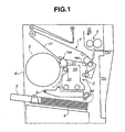
- Fig. 1 is an explanatory diagram of the overall configuration of an image forming apparatus according to the first embodiment of the invention.
- Fig. 2 is a block diagram illustrating circuit formation mainly focused on a power supply system for the image forming apparatus according to the first embodiment.
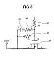
- Fig. 3 is a circuit diagram illustrating the detailed configuration of a power supply control circuit according to the first embodiment.
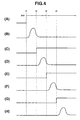
- Fig. 4 is a waveform chart explaining power supply timing according to the first embodiment.
- Fig. 5 is a block diagram illustrating the circuit configuration mainly focused on an image forming apparatus according to a second embodiment of the invention.
- Fig. 6 is a block diagram illustrating the configuration of a power supply control unit according to the second embodiment.
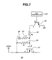
- Fig. 7 is a circuit diagram illustrating the detailed configuration of a power supply control circuit according to the second embodiment.
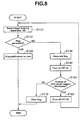
- Fig. 8 is a flowchart showing an example of one operation of the image forming apparatus according to the second embodiment.
- Fig. 9 is a flowchart showing an example of another operation of the image forming apparatus according to the second embodiment.
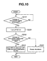
- Fig. 10 is a flowchart showing an example of one operation of the image forming apparatus according to a third embodiment of the invention.
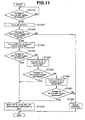
- Fig. 11 is a flowchart showing an example of another operation of the image forming apparatus according to the third embodiment.
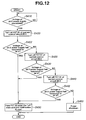
- Fig. 12 is a flowchart showing an example of a further operation of the image forming apparatus according to the third embodiment.
- an image forming apparatus for forming an image with an electrophotographic process, that includes: a power source; a first drive unit having a capacitative load and driving each part of the apparatus; a second drive unit having a capacitative load and driving each part of the apparatus; and a power supply control circuit that is provided on a power supply path between the power source and the second drive unit, that switches whether or not electric power is supplied to the second drive unit.
- the power supply control circuit includes: a field-effect transistor with its source connected to the power source side of the power supply path, and its drain connected to the second drive unit side of the power supply path; a first resistive element connected between the field-effect transistor's gate and source; a second resistive element and a capacitative element that are connected in parallel with the first resistive element, and connected with each other in series between the gate and the source.
- the image forming apparatus may be configured in such a manner that it further includes a switch that is located on power supply paths extending from the power source toward the first drive unit and the second drive unit respectively, at a position closer to the power source than the power supply control circuit, that switches whether or not electric power is supplied to the first or second drive unit, by bringing the first or second drive unit into conduction or non-conduction depending on the action of a specified part of the image forming apparatus.
- a switch that is located on power supply paths extending from the power source toward the first drive unit and the second drive unit respectively, at a position closer to the power source than the power supply control circuit, that switches whether or not electric power is supplied to the first or second drive unit, by bringing the first or second drive unit into conduction or non-conduction depending on the action of a specified part of the image forming apparatus.
- the switch may bring the first or second drive unit into conduction or non-conduction depending on the opening or closing action of a cover for protecting the outside surface of the image forming apparatus.
- an image forming apparatus for forming an image with an electrophotographic process, including: a drive unit having a capacitative load and driving each part of the apparatus; a power source for supplying electric power to the drive unit; a switch that is located on a power supply path extending from the power source toward the drive unit, that switches whether or not electric power is supplied to the drive unit, by bringing the drive unit into conduction or non-conduction depending on the action of a specified part of the image forming apparatus; and a power supply control circuit that is provided on the power supply path between the switch and the drive unit, that supplies electric power to the drive unit by becoming conductive in conjunction with the conductive state of the switch.
- the power supply control circuit includes: a field-effect transistor with its source connected to the power source side of the power supply path, and its drain connected to the second drive unit side of the power supply path; a first resistive element connected between the field-effect transistor's gate and source; a second resistive element and a capacitative element that are connected in parallel with the first resistive element, and connected with each other in series between the gate and the source.
- the switch may bring the drive unit into conduction or non-conduction depending on the opening or closing action of a cover for protecting the outside surface of the image forming apparatus.
- an image forming apparatus including: an engine unit for forming an image; a drive power source for generating a drive voltage to be supplied to the engine unit; an FET that is provided between the engine unit and the drive power source, that switches whether or not the drive voltage is supplied to the engine unit; a detector for detecting fluctuation in the drive voltage; and an FET controller for controlling whether the FET is turned on or off depending on fluctuation of the drive voltage detected by the detector.
- the image forming apparatus may include a plurality of FETs, and the FET controller may turn the FETs off sequentially when the detector detects fluctuation in the drive voltage.
- the above-described configuration is designed in such a way that if an error occurs in a component connected to any of the FETs, the drive voltage will return to its original state when the relevant FET is turned off. Therefore, with the above-described configuration, it is possible to determine the location where the error has occurred, and notify the user of the error details.
- the image forming apparatus may include a plurality of FETs, and the FET controller may turn the FETs off sequentially if the detector detects fluctuation of the drive voltage, and the FET controller then sequentially turns on the FETs that have been turned off.
- the above-described configuration is designed in such a way that if an error occurs in a component connected to any of the FETs, the drive voltage will decrease when the relevant FET is turned on. Therefore, with the above-described configuration, it is possible to determine the location where the error has occurred, and notify the user of the error details.
- the FET controller may turn the FET off when the drive voltage becomes lower than a specified value; and if the drive voltage becomes higher than the specified value when the FET has been turned off, the FET controller may judge that there is an error in the configuration of the engine unit connected to the FET.
- the FET in the image forming apparatus its source may be connected to the drive power source, its drain may be connected to the engine unit, and its gate may be connected to the FET controller, and the FET controller may include: a first resistive element provided between the source and the gate; and a second resistive element and a capacitative element connected in parallel with the first resistive element and located between the source and the gate.
- an image forming apparatus including: an engine unit for forming an image; a drive power source for generating a drive voltage to be supplied to the engine unit; an FET that is provided between the engine unit and the drive power source, that switches whether or not the drive voltage is supplied to the engine unit; an FET controller for controlling whether the FET is turned on or off depending on fluctuation of the drive voltage; and a flag controller for generating a flag when the FET controller turns the FET on; wherein if the drive voltage fluctuates when the flag controller has generated a flag and the FET controller has turned the FET on, the FET controller turns the FET off in the state where the flag has been generated.
- the above-described configuration is designed in such a way that when the FET has been turned on and the drive voltage has been supplied to the engine unit, and if an abnormal current is generated due to, for example, bad connection of the optional device and the drive voltage fluctuates, the FET controller turns the FET off in the state where the flag is on. Therefore, where the FET has been turned off due to generation of an abnormal current and, for example, the image forming apparatus is to be reset, it is possible in the above-described configuration to confirm the possibility of occurrence of an error when turning on the FET again, by checking the flag state.
- the expression “when X turns the FET on” includes the state where an attempt is being made to turn the FET on, the moment the FET is turned on, and immediately before turning on the FET, while the expression “when X has turned the FET on” (or any similar expression) includes the moment the FET is turned on and immediately after the FET has been turned on.
- the flag controller may clear the flag.
- the above-described configuration is designed in such a way that the flag is turned off if there is no error. Accordingly, if there is an error, the FET is turned off in the state where the flag is on. If there is no error, the flag is cleared. Therefore, in the above-described configuration, even in the case where an abnormal current is generated every time the FET is turned on due to, for example, bad connection of the optional device, it is possible to prevent the generation of an abnormal current by not turning the FET on.
- the flag controller clear the flag. Moreover, if in the image forming apparatus the drive voltage becomes lower than a specified value when the FET controller has turned the FET on, the FET controller may turn the FET off in the state where the flag has been generated.
- the image forming apparatus may further include a notifying unit for giving a specified notice to a user if the flag has been generated when the FET controller turns the FET on,
- Fig. 1 is an explanatory diagram of the overall configuration of an image forming apparatus according to the first embodiment of the invention.
- the image forming apparatus shown in Fig. 1 forms full-color images by applying toners of four colors - yellow (Y), magenta (M), cyan (C), and black (K) - one over another, and also forms black-and-white images by using only back toner.
- This image forming apparatus is configured in such a way that when a picture signal is sent from an external apparatus (not shown in the drawing) such as a host computer, each component operates under the control of a main controller and an engine controller, and forms (i.e., prints) images corresponding to the picture signal on sheets S such as copying paper, transfer paper, paper, and OHP transparent sheets.
- a photoreceptor unit 2 In the image forming apparatus shown in Fig. 1, a photoreceptor unit 2, a development unit 3, an intermediate transfer unit 4, and a fixing unit 5 are respectively configured in such a way that they can be attached to and detached from a main body (housing 6) of the apparatus.
- a photoreceptor 21 in a photoreceptor unit 2 rotates in the direction indicated with an arrow in Fig. 1 in the state where the respective units listed above are mounted on the main body 6.
- a charging member 22, the rotary development unit 3, and a cleaner 23 are respectively located around the photoreceptor 21 along its rotating direction.
- the rotary development member 3 contains four development units corresponding to the four colors Y, M, C, and K.
- the charging member 22, to which a charge bias is applied uniformly charges the outside surface of the photoreceptor 21.
- the cleaner 23 cleans the photoreceptor 21 by scraping off the remaining toner attached to the outside surface of the photoreceptor 21 after primary transfer.
- a light exposure unit 8 emits laser beam L according to the picture signal sent from the engine controller and has the outside surface of the photoreceptor 21 exposed to the laser beam L, forming an electrostatic latent image on the photoreceptor 21 corresponding to the picture signal.
- the electrostatic latent image formed as described above undergoes toner development via the rotary development unit 3.
- the electrostatic latent image on the photoreceptor 21 is made visible with toners of the four colors Y, M, C, and K.
- the thus developed toner image undergoes primary transfer by which the toner image is transferred onto an intermediate transfer belt 41 of the intermediate transfer unit 4 in a primary transfer area TR1.
- the image formed on the intermediate transfer belt 41 then undergoes secondary transfer in a specified secondary transfer area TR2 by which the image is transferred onto a sheet S taken from a cassette 9.
- the sheet S on which the image is formed in the above-described manner then passes through the fixing unit 5 and is carried to a catch tray located on the top surface of the main body 6.
- Fig. 2 is a block diagram explaining the circuit layout, mainly focusing on a power supply system of the image forming apparatus.
- the image forming apparatus according to this first embodiment operates by receiving supply of an alternating current (AC) voltage (100 V) from a commercial power source (AC source).
- AC alternating current
- a low voltage power source 50 receives the AC voltage from the commercial power source via a power source switch and generates three kinds of direct current (DC) voltages (3.3V, 5V, and 24V).
- the respective power 3.3V, 5V, and 24V is supplied via a second main board 51 to each component of the image forming apparatus.
- the 3.3V power is supplied to a first main board 52 including a main controller.
- the 5V power is supplied to a thermistor unit 53, a batch sensor 54, an R/W module 55, a photosensor 56, a photoreceptor drive motor unit 57, a general drive motor unit 58, and a drive circuit board (DRV board) 59 respectively.
- the 5V power is also supplied via a 5V interlock switch in an interlock switch unit 71, to the light exposure unit 8.
- the 24V power is supplied to the photoreceptor 21, a high voltage power source 60, the photoreceptor drive motor unit 57, the general drive motor unit 58, a secondary transfer roller adjoining clutch 61, an intermediate transfer belt cleaner adjoining clutch 62, a development drive motor unit 63, a rotary drive motor unit 64, an eraser lamp unit 65, an ozone fan unit 66, a toner fan unit 67, a cooling fan 68, a paper-feed-related clutch 69, and a scanner motor 70.
- Each of these components, including the high voltage power source 60 has a capacitative load. Switches using bipolar transistors or field-effect transistors are provided as appropriate on power supply paths (wires) that connect these components with the 24V power source.
- the photoreceptor 21, the high voltage power source 60, the photoreceptor drive motor unit 57, the general drive motor unit 58, the secondary transfer roller adjoining clutch 61, the intermediate transfer belt cleaner adjoining clutch 62, the development drive motor unit 63, and the rotary drive motor unit 64 receive the supply of the 24V power via 24V interlock switches 72, 73, and 74 in the interlock switch unit 71. Accordingly, when a cover, such as a full-face cover or a side-face cover, of the image forming apparatus is opened, each interlock switch opens in conjunction with the opening action of the cover, thereby stopping the 24V power supply.
- the eraser lamp unit 65, the ozone fan unit 66, the toner fan unit 67, the cooling fan 68, and the paper-feed-related clutch 69 correspond to the "first drive unit.”
- the photoreceptor 21, the high voltage power source 60, the photoreceptor drive motor unit 57, the general drive motor unit 58, the secondary transfer roller adjoining clutch 61, the intermediate transfer belt cleaner adjoining clutch 62, the development drive motor unit 63, the rotary drive motor unit 64, and the scanner motor 70 correspond to the "second drive unit.”
- the interlock switch unit 71 corresponds to the "switch.”
- a power supply control circuit 80a containing a field-effect transistor is provided on the supply path connecting the high voltage power source 60 as the "second drive unit" with the 24V power source. Also, a power supply control circuit 80b containing a field-effect transistor is provided on the supply path connecting the photoreceptor drive motor unit 57, the general drive motor unit 58, the secondary transfer roller adjoining clutch 61, the intermediate transfer belt cleaner adjoining clutch 62, the development drive motor unit 63, and the rotary drive motor unit 64, respectively with the 24V power source.
- These power supply control circuits 80a and 80b are provided on the power supply paths between the interlock switch unit 71 and the respective drive units, and switch whether or not the electric power is supplied to the drive units under the control of the first main board 52 as control means, and inhibit inflow of an inrush current into the drive units when the interlock switch unit 71 becomes conductive. Consequently, it is possible to prevent an excessive inrush current from flowing into the drive units when opening and closing the cover, such as a full-face cover or a side-face cover, of the image forming apparatus.
- a power supply control circuit 80c containing a field-effect transistor is provided on the supply path connecting the scanner motor 70 as the "second drive unit" with the 24V power source.
- Fig. 3 is a circuit diagram explaining the detailed configuration of the power supply control circuit 80a.
- the power supply control circuit 80a shown in Fig. 3 includes a field-effect transistor 81, resistive elements 82, 83, and 84, and a capacitative element 85.
- the source of the field-effect transistor 81 is connected to the power source (DC 24V) side of the power supply path, and its drain is connected to the drive unit side of the power supply path.
- a P-channel enhancement MOSFET is used as the field-effect transistor 81.
- the resistive element 83 (first resistive element) is connected between the gate and source of the field-effect transistor 81, works together with the resistive element 82 to divide the voltage from the power source, and generates an appropriate gate voltage (12V in this example).
- the resistive element 84 (second resistive element) and the capacitative element 85 are connected in series with each other and also connected in parallel with the resistive element 83, and are located between the gate and source of the field-effect transistor 81.
- the resistance value and capacitance value of the elements are set, for example, as follows: the resistive elements 82 and 83, each with the resistance value 100 k ⁇ , the resistive element 84 with the resistive value 27 k ⁇ , and the capacitative element 85 with the capacitance value 0.1 ⁇ F.
- the power supply control circuits 80b and 80c are configured in a manner similar to those of the power supply circuit 80a.
- Fig. 4 shows waveform charts schematically explaining power supply timing.
- waveform chart (A) when the interlock switch unit 71 enters the ON state and the voltage is applied to the switch from the 24V power source at time t1, the eraser lamp unit 65 and other components, as the first drive unit, have their capacitive loads charged at that time t1, generating an inrush current, and then return to the steady state as shown in waveform chart (B).
- waveform chart (C) a specified voltage is applied to the gate of the field-effect transistor 81 included in the power supply control circuit 80b, and the transistor 81 enters the ON state.
- waveform chart (D) the photoreceptor drive motor unit 57 and other components, as the second drive unit, have their capacitative loads charged, generating an inrush current, and then return to the steady state.
- waveform chart (E) a specified voltage is applied to the gate of the field-effect transistor 81 included in the power supply control circuit 80c, and the transistor 81 enters the ON state.
- waveform chart (F) the scanner motor 70, as the second drive unit, has its capacitative load charged, generating an inrush current, and then returns to the steady state.
- waveform chart (G) Next at time t4 as shown in waveform chart (G), a specified voltage is applied to the gate of the field-effect transistor 81 included in the power supply control circuit 80a, and the transistor 81 enters the ON state. Consequently, as shown in waveform chart (H), the high voltage power source 60, as the second drive unit, has its capacitative load charged, generating an inrush current, and then returns to the steady state.
- the power supply control circuits 80a, 80b, and 80c are provided In the first embodiment, it is possible to prevent the passage of an inrush current when the field-effect transistor 81 turns on for a moment in the state where the interlock switch unit 71 enters the ON state and the 24V power is on. Because the series circuit formed by the resistive element 84 and the capacitative element 85 is provided, when the interlock switch unit 71 is turned on, no potential difference occurs between the gate and source of the field-effect transistor 81, and electric current does not pass through the field-effect transistor 81 immediately. As a result, it is possible to prevent unexpected power supply to the second drive unit, and also prevent the occurrence of an excessive inrush current.
- Fig. 5 is a block diagram explaining the circuit configuration, mainly focusing on a power supply system for an image forming apparatus according to a second embodiment of the invention.
- the image forming apparatus according to this second embodiment operates by receiving the supply of an alternating current (AC) voltage (100 V) from a commercial power source (AC source).
- AC alternating current
- AC source commercial power source
- a low voltage power source 50 receives the AC voltage from the commercial power source via a power source switch and generates three kinds of direct current (DC) voltages (3.3V, 5V, and 24V), which are examples of drive voltages.
- the respective power 3.3V, 5V, and 24V is supplied via a second main board 51 to each component of the image forming apparatus.
- the 3.3V power is supplied to a first main board 52 including a main controller.
- the 5V power is supplied to a thermistor unit 53, a batch sensor 54, an R/W module 55, a photosensor 56, a photoreceptor drive motor unit 57, a general drive motor unit 58, and a drive circuit board (DRV board) 59 respectively.
- the 5V power is also supplied via a 5V interlock switch in an interlock switch unit 71, to a light exposure unit 8.
- the 24V power is supplied to the photoreceptor 21, a high voltage power source 60, the photoreceptor drive motor unit 57, the general drive motor unit 58, a secondary transfer roller adjoining clutch 61, an intermediate transfer belt cleaner adjoining clutch 62, a development drive motor unit 63, a rotary drive motor unit 64, an eraser lamp unit 65, an ozone fan unit 66, a toner fan unit 67, a cooling fan 68, a paper-feed-related clutch 69, and a scanner motor 70 respectively.
- Each of these components, including the high voltage power source 60 has a capacitative load, Switches using bipolar transistors or field-effect transistors are provided as appropriate on power supply paths (wires) that connect these components with the 24V power source.
- the photoreceptor 21, the high voltage power source 60, the photoreceptor drive motor unit 57, the general drive motor unit 58, the secondary transfer roller adjoining clutch 61, the intermediate transfer belt cleaner adjoining clutch 62, the development drive motor unit 63, and the rotary drive motor unit 64 receive the supply of the 24V power via 24V interlock switches 72, 73, and 74 in the interlock switch unit 71. Accordingly, when a cover, such as a full-face cover or a side-face cover, of the image forming apparatus is opened, each interlock switch opens in conjunction with the opening action of the cover, thereby stopping the 24V power supply.
- a power supply control circuit 80-1 containing a field-effect transistor (FET) is provided on the supply path connecting the high voltage power source 60 with the 24V power source.
- a power supply control circuit 80-2 is provided on the supply path connecting the photoreceptor drive motor unit 57, the general drive motor unit 58, the secondary transfer roller adjoining clutch 61, the intermediate transfer belt cleaner adjoining clutch 62, the development drive motor unit 63, and the rotary drive motor unit 64, all of which are examples of an engine unit, respectively with the 24V power source.
- a power supply control circuit 80-3 containing a field-effect transistor is provided on the supply path connecting the scanner motor 70 as a "drive unit" with the 24V power source.
- These power supply control circuits 80-1 to 80-3 are provided on the power supply paths extending between the interlock switch unit 71 and the respective drive units, switch whether or not the power is supplied to the drive units under the control of the first main board 52 which is a control means, and inhibit inflow of an inrush current into the drive units when the interlock switch unit 71 becomes conductive. Consequently, it is possible to prevent an excessive inrush current from flowing into the drive units when opening and closing the cover, such as a full-face cover or a side-face cover, of the image forming apparatus.
- Fig. 6 is a block diagram illustrating the configuration of a power source controller 200.
- the power source controller 200 includes a detector 100, an FET controller 120, a flag controller 130, and nonvolatile memory 140.
- the detector 110 detects voltage fluctuation of the 24V power.
- the detector 110 judges that the 24V power has fluctuated, and notifies the FET controller 120 to that effect.
- the FET controller 120 controls, in accordance with an instruction from the main board 52 or the notification from the detector 110, whether the FET included in the power supply control circuit 80 is turned on or off.
- the flag controller 130 generates a flag in the nonvolatile memory 140 or clears the generated flag in accordance with an instruction from the main board 52 and/or the FET controller 120.
- Fig. 7 is a circuit diagram explaining the detailed configuration of the power supply control circuits 80-1 to 80-3.
- the power supply control circuit 80 shown in Fig. 7 includes an FET 81, resistive elements 82, 83, and 84, a capacitative element 85, and a bipolar transistor 86.
- the source of the FET 81 is connected to the power source (DC 24V) side of the power supply path, and its drain is connected to the drive unit side of the power supply path.
- a P-channel enhancement MOSFET is used as the FET 81.
- the resistive element 83 (first resistive element) is connected between the gate and source of the FET 81, works together with the resistive element 82 to divide the voltage from the power source, and generates an appropriate gate voltage (12V in this example).
- the resistive element 84 (second resistive element) and the capacitative element 85 are connected in series with each other and also connected in parallel with the resistive element 83 and located between the gate and source of the FET 81.
- the resistance value and the capacitance value of the respective elements are set, for example, as follows: the resistive elements 82 and 83, each with the resistance value 100 k ⁇ , the resistive element 84 with the resistive value 27 k ⁇ , and the capacitative element 85 with the capacitance value 0.1 ⁇ F.
- the collector of the bipolar transistor 86 is connected via the resistive element 82 to the gate of the FET 81, its emitter is grounded, and its base is connected to the FET controller 120.
- the bipolar transistor 86 controls the gate voltage of the FET 81.
- the FET controller 120 sets the base voltage to 5V to have the bipolar transistor 86 enter the ON state, and decreases the gate voltage of the FET 81.
- the FET controller 120 sets the base voltage to 0V to have the bipolar transistor 86 enter the OFF state, and increases the gate voltage of the FET 81.
- Fig. 8 is a flowchart showing an example of one operation of the image forming apparatus according to the second embodiment.
- An example of the operation of the image forming apparatus according to the second embodiment in the case where fluctuation of the 24V power supply has occurred will be described below with reference to Figs. 5 to 8.
- the operation of the image forming apparatus will be explained for the case where the power supply control circuit 80-2 supplies the 24V power to an optional device 100, an example of the engine unit, in the situation where a user has incorrectly connected the optional device 100 to the image forming apparatus and a short circuit has occurred in the optional device 100.
- the flag controller 130 checks whether a flag has been generated in the nonvolatile memory 140 or not (S112).
- the flag controller 130 notifies the main board 52 to that effect, and the main board 52 then notifies the user that there is an error, for example, in a component connected downstream of the power supply control circuit 80-2, by displaying a notice on a display unit such as a liquid crystal display (S120).
- the flag controller 130 determines whether no flag is generated in the nonvolatile memory (S112: NO)
- the flag controller 130 generates a flag in the nonvolatile memory (S130)
- the FET controller 120 turns on the FET 81 of the power supply control circuit 80-2.
- the FET controller 120 may turn the FET 81 on almost at the same time as the flag controller 130 generates the flag.
- the FET 81 of the power supply control circuit 80-2 enters the ON state, the 24V power is supplied to the optional device 100. Since a short circuit has occurred in the optional device 100, an abnormal current passes through the optional device 100 and the voltage of the 24V power supply decreases. If the voltage of the 24V power supply decreases to 21.6V or lower, the detector 110 judges that the voltage of the 24V power supply has decreased, and notifies the FET controller 120 to that effect.
- the FET controller 120 turns off the FET 81 of the power supply controller circuit 80-2 (S160). Specifically speaking, the FET controller 120 sets the base voltage of the bipolar transistor 86 to 0V to turn the bipolar transistor 86 off, and then increases the gate voltage of the FET 81. Consequently, the gate voltage of the FET 81 exceeds its threshold voltage and the FET 81 enters the OFF state.
- the flag controller 130 checks again whether a flag has been generated in the nonvolatile memory 140 or not (S112). Since the image forming apparatus is reset in S110 in the state where the flag generated in S130 is stored in the nonvolatile memory 140, the flag controller 130 notifies the main board 52 that the flag has been generated in the nonvolatile memory 140, and the main board 52 notifies the user to that effect (S120).
- the flag controller 130 clears the flag generated in the nonvolatile memory in S130 (S170), and the image forming apparatus stands by for an external print instruction. If the voltage of the 24V power supply does not increase for, for example, a certain period of time (such as 200 ms) after the FET 81 has been turned on, the flag controller 130 judges that there is no error downstream of the FET 81, and then clears the flag.
- a flag is generated in the nonvolatile memory 14 when turning on the FET 81; and if there is no error after the FET 81 has been turned on, the flag is cleared. If an error occurs when the FET 81 is on, the FET 81 is turned off in the state where the flag has been generated. Accordingly, by checking the flag state when resetting the image forming apparatus, the user can judge whether or not an error occurred before the reset. Therefore, since the image forming apparatus according to the second embodiment can confirm that there is the possibility of occurrence of an error if the FET were to be turned on again, it is possible to prevent the image forming apparatus from being repeatedly reset due to the occurrence of an error.
- Fig. 9 is a flowchart showing an example of another operation of the image forming apparatus according to the second embodiment. Another example of the operation of the image forming apparatus according to the second embodiment in the case where fluctuation of the 24V power supply has occurred will be described below with reference to Figs. 5 to 7, and Fig. 9.
- the FET controller 120 turns on the FETs 81 of the power supply control circuits 80-1 to 80-3 sequentially and the 24V power is sequentially supplied to each component of the engine unit.
- the flag controller 130 checks whether a flag has been generated in the nonvolatile memory 140 or not (S312),
- the flag controller 130 notifies the main board 52 to that effect, and the main board 52 then notifies the user that there is an error, for example, in a component connected downstream of the power supply control circuit 80-2, by displaying a notice on a display unit such as a liquid crystal display (S320).
- the flag controller 130 determines whether no flag is generated in the nonvolatile memory (S312: NO). If no flag is generated in the nonvolatile memory (S312: NO), the flag controller 130 generates first to third flags in the nonvolatile memory 140 corresponding to the power supply control circuits 80-1 to 80-3 (S330). The FET controller 120 first turns on the FET 81 of the power supply control circuit 80-1 (S340).
- the FET controller 120 turns off the FETs 81 of the power supply control circuits 80-1 to 80-3 (S370).
- the flag controller 130 checks again whether a flag has been generated in the nonvolatile memory 140 or not (S312). Since the image forming apparatus is reset in S310 in the state where the first to third flags generated in S330 are stored in the nonvolatile memory 140, the flag controller 130 notifies the main board 52 that the first to third flags have been generated in the nonvolatile memory 140. Then, since the first to third flags have been generated, the main board 52 judges that an error has occurred downstream of the power supply control circuit 80-1, and notifies the user to that effect (S320).
- the flag controller 130 judges that there is no error downstream of the power supply control circuit 80-1, and then clears the first flag generated in the nonvolatile memory 140 in S330 (S344).
- the FET controller 120 turns on the FET 81 of the power supply control circuit 80-2 (S350). If the voltage of the 24V power supply decreases after the FET 81 of the power supply control circuit 80-2 has been turned on (S352: Yes), the FET controller 120 turns off the FETs 81 of the power supply control circuits 80-1 to 80-3 (S370).
- the flag controller 130 checks again whether a flag has been generated in the nonvolatile memory 140 or not (S312). Since the image forming apparatus is reset in S310 in the state where the second and third flags generated in S330 are stored in the nonvolatile memory 140, the flag controller 130 notifies the main board 52 that the second and third flags have been generated in the nonvolatile memory 140. Then, since the second and third flags have been generated, the main board 52 judges that an error has occurred downstream of the power supply control circuit 80-2, and notifies the user to that effect (S320).
- the flag controller 130 judges that there is no error downstream of the power supply control circuit 80-2, and then clears the second flag generated in the nonvolatile memory 140 in S330 (S354).
- the FET controller 120 turns on the FET 81 of the power supply control circuit 80-3 (S360). If the voltage of the 24V power supply decreases after the FET 81 of the power supply control circuit 80-3 has been turned on (S362: Yes), the FET controller 120 turns off the FETs 81 of the power supply control circuits 80-1 to 80-3 (S370).
- the flag controller 130 checks again whether a flag has been generated in the nonvolatile memory 140 or not (S312). Since the image forming apparatus is reset in S310 in the state where the third flag generated in S330 is stored in the nonvolatile memory 140, the flag controller 130 notifies the main board 52 that the third flag has been generated in the nonvolatile memory 140. Then, since the third flag has been generated, the main board 52 judges that an error has occurred downstream of the power supply control circuit 80-3, and notifies the user to that effect (S320).
- the flag controller 130 judges that there is no error downstream of the power supply control circuit 80-3, and then clears the third flag generated in the nonvolatile memory 140 in S330 (S364). As a result, all the first to third flags are cleared and the image forming apparatus stands by for an external print instruction.
- the image forming apparatus can identify the location where the error has occurred, out of the components connected to the plural FETs, and notify the user to that effect.
- the power source controller 200 includes the detector 110 and the FET controller 120.
- any parts overlapping with the descriptions of the first and second embodiments will be omitted.
- Fig. 10 is a flowchart showing an example of one operation of the image forming apparatus according to the third embodiment.
- An example of the operation of the image forming apparatus in the case where fluctuation of the 24V power supply has occurred will be described below with reference to Figs. 7 and 10.
- the operation of the image forming apparatus will be explained about the case where the power supply control circuit 80-2 supplies the 24V power to the optional device 100 in the situation where the user has incorrectly connected the optional device 100 to the image forming apparatus and a short circuit has occurred in the optional device 100.
- the 24V power is supplied to the optional device 100. Since a short circuit has occurred in the optional device 100, an abnormal current passes through the optional device 100 and the voltage of the 24V power supply decreases. If the voltage of the 24V power supply decreases to 21.6V or lower, the detector 110 judges that the voltage of the 24V power supply has decreased, and notifies the FET controller 120 to that effect (S21 0: Yes). If the voltage of the 24V power supply is higher than 21.6V, the detector judges that the 24V power supply is stable, and then continues checking(S21 0: No).
- the FET controller 120 turns off the FET 81 of the power supply controller circuit 80-2. Specifically speaking, the FET controller 120 sets the base voltage of the bipolar transistor 86 to 0V to turn the bipolar transistor 86 off, and then increases the gate voltage of the FET 81. Consequently, the gate voltage of the FET 81 exceeds its threshold voltage and the FET 81 enters the OFF state.
- the FET controller 120 After the FET controller 120 has turned off the FET 81 of the power supply control circuit 80-2, the 24V power is not supplied to the short-circuited optional device 100 (see Fig. 5) and the abnormal current stops. As a result, the voltage of the 24V power supply recovers to 24V (S230: Yes). If the voltage of the 24V power supply has recovered to 24V, the FET controller 120 turns the FET 81 off and judges that an error has occurred in one of the components connected to the power supply control circuit 80-2, and notifies the user to that effect (S240). On the other hand, if the voltage of the 24V power supply does not recover to 24V even after the FET controller 120 has turned the power supply control circuit 80-2 off (S230: No), the low voltage power source 50 cuts off the 24V power supply.
- whether or not the 24V power is supplied to the engine unit is controlled depending on fluctuation of the voltage value, through the operation described above. Accordingly, even if a short circuit or leakage occurs in any of the components of the engine unit and an abnormal current is generated, it is possible to appropriately control the supply of the 24V power to each component without cutting off the 24V power supply.
- the series circuit formed by the resistive element 84 and the capacitative element 85 inhibits a sudden increase of the abnormal current in the engine unit, it is possible to turn the FET 81 off as appropriate and control the supply of the 24V power to the engine unit.
- Fig. 11 is a flowchart showing another example operation of the image forming apparatus according to the third embodiment. Another example of the operation of the image forming apparatus according to the third embodiment in the case where fluctuation of the 24V power supply has occurred will be described below with reference to Figs. 7 and 11.
- the 24V power is supplied to the engine unit. If an abnormal current occurs at this moment in any of the components connected to the power supply control circuits 80-1 to 80-3, the voltage of the 24V power supply decreases. If the voltage of the 24V power supply decreases to 21.6V or lower, the detector 110 judges that the voltage of the 24V power supply has decreased, and notifies the FET controller 120 to that effect (S1310: Yes).
- a case where an abnormal current occurs is, for example, when a short circuit occurs in the optional device 100 in the situation where the user has incorrectly connected the optional device 100 to the image forming apparatus.
- the FET controller 120 turns off all the FETs 81 of the power supply controller circuits 80-1 to 80-3 (S1320). Specifically speaking, the FET controller 120 sets the base voltage of the bipolar transistor 86 to 0V to turn the bipolar transistor 86 off, and then increases the gate voltage of the FETs 81. Consequently, the gate voltages of the FETs 81 exceed their threshold voltage and the FETs 81 enter the OFF state.
- the 24V power is not supplied to the short-circuited optional device 100 (see Fig. 5), and the abnormal current stops. As a result, the voltage of the 24V power supply recovers to 24V (S1330: Yes). If the voltage of the 24V power supply does not recover to 24V even after the FET controller 120 has turned off all the FETs of the power supply control circuits 80-1 to 80-3 (S1330; No), the low voltage power source 50 cuts off the 24V power supply (S1380).
- the FET controller 120 After the FET controller 120 has turned all the FETs 81 off and the 24V power supply has recovered to 24V, the FET controller 120 turns on the FETs 81 of the power supply control circuits 80-1 to 80-3 sequentially. In this example, the FET controller 120 first turns on the FET 81 of the power supply control circuit 80-1 (S1340).
- the detector 110 checks the voltage of the 24V power supply, If the voltage of the 24V power supply has decreased (S1342: Yes), the FET controller 120 judges that an error has occurred in one of the components connected to the power supply control circuit 80-1, turns all the FETs 81 off, and notifies the user to that effect (S1370).
- the FET controller 120 judges that there is no error in the components connected to the power supply control circuit 80-1. Subsequently, the FET controller 120 turns on the FET 81 of the power supply control circuit 80-2 (S1350). At this moment, the FET controller 120 may turn on the FET 81 of the power supply control circuit 80-2 after turning off the FET 81 of the power supply control circuit 80-1.
- the detector 110 checks the voltage of the 24V power supply. If the voltage of the 24V power supply has decreased (S1352: Yes), the FET controller 120 judges that an error has occurred in one of the components connected to the power supply control circuit 80-2, turns all the FETs 81 off, and notifies the user to that effect (S1370).
- the FET controller 120 judges that there is no error in the components connected to the power supply control circuit 80-2. Subsequently, the FET controller 120 turns on the FET 81 of the power supply control circuit 80-3 (S1360). At this moment, the FET controller 120 may turn on the FET 81 of the power supply control circuit 80-3 after turning off the FET(s) 81 of the power supply control circuit(s) 80-1 and/or 80-2.
- the detector 110 checks the voltage of the 24V power supply. If the voltage of the 24V power supply has decreased (S1362: Yes), the FET controller 120 judges that an error has occurred in one of the components connected to the power supply control circuit 80-3, turns all the FETs 81 off, and notifies the user to that effect (S1370).
- the FET controller 120 judges that it is impossible to identify the location where the error has occurred, and the low voltage power source 50 cuts off the 24V power supply (S1380).
- the image forming apparatus can identify the location where an error has occurred, out of the components connected to the plural FETs, and notify the user to that effect.
- Fig. 12 is a flowchart showing an example of a further operation of the image forming apparatus according to the third embodiment.
- a further example of the operation of the image forming apparatus according to the third embodiment in the case where fluctuation of the 24V power supply has occurred will be described below with reference to Figs. 7 and 12.
- the 24V power is supplied to the engine unit. If an abnormal current occurs at this moment in any of the components connected to the power supply control circuits 80-1 to 80-3, the voltage of the 24V power supply decreases. If the voltage of the 24V power supply decreases to 21.6V or lower, the detector 110 judges that the voltage of the 24V power supply has decreased, and notifies the FET controller 120 to that effect (S410: Yes).
- a case where an abnormal current occurs is, for example, when a short circuit occurs in the optional device 100 in the situation where the user has incorrectly connected the optional device 100 to the image forming apparatus.
- the FET controller 120 sequentially turns off all the FETs 81 of the power supply controller circuits 80-1 to 80-3. In this example, the FET controller 120 first turns off the FET 81 of the power supply control circuit 80-1 (S420).
- the detector 110 checks the voltage of the 24V power supply. If the voltage of the 24V power supply has recovered to 24V (S442: Yes), the FET controller 120 judges that an error has occurred in one of the components connected to the power supply control circuit 80-1, turns all the FETs 81 off, and notifies the user to that effect (S450).
- the FET controller 120 judges that there is no error in the components connected to the 24V power supply control circuit 80-1. Subsequently, the FET controller 120 turns off the FET 81 of the power supply control circuit 80-2 (S430). At this moment, the FET controller 120 may turn off the FET 81 of the power supply control circuit 80-2 after turning on the FET 81 of the power supply control circuit 80-1.
- a predetermined period of time for example, 10 ms to 200 ms
- the detector 110 checks the voltage of the 24V power supply. If the voltage of the 24V power supply has recovered to 24V (S432: Yes), the FET controller 120 judges that an error has occurred in any of the components connected to the power supply control circuit 80-2, turns all the FETs 81 off, and notifies the user to that effect (S450).
- the FET controller 120 judges that there is no error in the components connected to the 24V power supply control circuit 80-2. Subsequently, the FET controller 120 turns off the FET 81 of the power supply control circuit 80-3 (S440). At this moment, the FET controller 120 may turn off the FET 81 of the power supply control circuit 80-3 after turning on the FET(s) 81 of the power supply control circuit(s) 80-1 and/or 80-2.
- a predetermined period of time for example, 10 ms to 200 ms
- the detector 110 checks the voltage of the 24V power supply. If the voltage of the 24V power supply has recovered to 24V (S442: Yes), the FET controller 120 judges that an error has occurred in one of the components connected to the power supply control circuit 80-3, turns all the FETs 81 off, and notifies the user to that effect (S450).
- the FET controller 120 judges that it is impossible to identify the location where the error has occurred, and the low voltage power source 50 cuts off the 24V power supply (S460).
- the image forming apparatus can identify the location where an error has occurred, out of the components connected to the plural FETs, and notify the user to that effect.
Landscapes
- Engineering & Computer Science (AREA)
- Microelectronics & Electronic Packaging (AREA)
- Physics & Mathematics (AREA)
- General Physics & Mathematics (AREA)
- Control Or Security For Electrophotography (AREA)
Abstract
An image forming apparatus for forming an image with an electrophotographic process, that includes: a power source; a first drive unit having a capacitative load and driving each part of the apparatus; a second drive unit having a capacitative load and driving each part of the apparatus: and a power supply control circuit that is provided on a power supply path between the power source and the second drive unit, that switches whether or not electric power is supplied to the second drive unit. The power supply control circuit includes: a field-effect transistor with its source connected to the power source side of the power supply path, and its drain connected to the second drive unit side of the power supply path; a first resistive element connected between the field-effect transistor's gate and its source; a second resistive element and a capacitative element that are connected in parallel with the first resistive element, and connected with each other in series between the gate and the source.
Description
- This application relates to and claims priority from Japanese Patent Applications 2005-011856, 2005-011883, and 2005-011867, filed on January 19, 2005, and Japanese Patent Application No. 2005-092447, filed on March 28, 2005, the entire disclosure of which is incorporated herein by reference.
- The present invention relates to an image forming apparatus such as a printer, a copying machine, or a facsimile.
- A related art example of an image forming apparatus with an electrophotographic process, such as a printer, copying machine, or facsimile, is disclosed in JP-A-2003-54097. This type of image forming apparatus generally uses two or more kinds of power supply voltages as power sources for driving an internal circuit. For example, components containing a microprocessor or the like, such as a controller for controlling the entire operation of the image forming apparatus, and a logic circuit that executes image signal processing and other functions, need a low-voltage (for example, 5 V) power source, while mechanisms such as a motor for driving a photosensitive drum and a paper-feed mechanism, and a laser unit as a light source for light exposure, that require high electric power need a high-voltage (for example, 24 V) power source.
- In a general image forming apparatus, a switch that opens or closes a circuit in conjunction with the opening or closing action of a cover for covering the internal content of the main body is provided on the circuit in order to cut off power supply to a motor and other components when the cover is opened in the case where a malfunction (such as paper jamming) has occurred. However, when the switch opens the circuit, cutting off the power, and then closes the circuit again, a high inrush current sometimes flows into a condenser (capacitative load) mounted on a motor control substrate or similar, which is the power supply destination. The upper limit is set for a current value at which current can be passed through the switch, and the inrush current sometimes exceeds that upper limit. With that kind of malfunction problem, a step to avoid a high inrush current flowing into the switch is taken by providing, in addition to the above-mentioned switch, electronic switches such as field-effect transistors (FET) on a power supply path in order to divide the power supply destination, and turning on the respective transistors sequentially at certain time intervals. Moreover, after the cover has been opened and then closed in order to, for example, mount an optional device, in other words, after the switch and the FETS have been opened to cut off power, and then closed again, and if a short-circuit occurs due to, for example, inappropriate mounting of the optional device, an abnormal current may still flow into the optional device.
- However, the image forming apparatus disclosed in JP-A-2003-54097 has the problem of incapability to appropriately control a power supply voltage in a component connected to the FETs if an abnormal current is generated in the power supply path due to a short circuit or similar.
- According to an aspect of the invention, provided is an image forming apparatus for forming an image with an electrophotographic process, that includes: a power source; a first drive unit having a capacitative load and driving each part of the apparatus: a second drive unit having a capacitative load and driving each part of the apparatus: and a power supply control circuit that is provided on a power supply path between the power source and the second drive unit, that switches whether or not electric power is supplied to the second drive unit. The power supply control circuit includes: a field-effect transistor with its source connected to the power source side of the power supply path, and its drain connected to the second drive unit side of the power supply path; a first resistive element connected between the field-effect transistor's gate and source; a second resistive element and a capacitative element that are connected in parallel with the first resistive element, and connected with each other in series between the gate and the source.
- According to another aspect of the invention, provided is an image forming apparatus for forming an image with an electrophotographic process, including: a drive unit having a capacitative load and driving each part of the apparatus; a power source for supplying electric power to the drive unit; a switch that is located on a power supply path extending from the power source toward the drive unit, that switches whether or not electric power is supplied to the drive unit, by bringing the drive unit into conduction or non-conduction depending on the action of a specified part of the image forming apparatus; and a power supply control circuit that is provided on the power supply path between the switch and the drive unit, that supplies electric power to the drive unit by becoming conductive in conjunction with the conductive state of the switch. The power supply control circuit includes: a field-effect transistor with its source connected to the power source side of the power supply path, and its drain connected to the second drive unit side of the power supply path; a first resistive element connected between the field-effect transistor's gate and source; a second resistive element and a capacitative element that are connected in parallel with the first resistive element, and connected with each other in series between the gate and the source.
- According to a further aspect of the invention, provided is an image forming apparatus including: an engine unit for forming an image; a drive power source for generating a drive voltage to be supplied to the engine unit; an FET that is provided between the engine unit and the drive power source, that switches whether or not the drive voltage is supplied to the engine unit; a detector for detecting fluctuation in the drive voltage; and an FET controller for controlling whether the FET is turned on or off depending on fluctuation of the drive voltage detected by the detector.
- According to a still further aspect of the invention, provided is an image forming apparatus including: an engine unit for forming an image; a drive power source for generating a drive voltage to be supplied to the engine unit; an FET that is provided between the engine unit and the drive power source, that switches whether or not the drive voltage is supplied to the engine unit; an FET controller for controlling whether the FET is turned on or off depending on fluctuation of the drive voltage; and a flag controller for generating a flag when the FET controller turns the FET on; wherein if the drive voltage fluctuates when the flag controller has generated a flag and the FET controller has turned the FET on, the FET controller turns the FET off in the state where the flag has been generated.
- Fig. 1 is an explanatory diagram of the overall configuration of an image forming apparatus according to the first embodiment of the invention.
- Fig. 2 is a block diagram illustrating circuit formation mainly focused on a power supply system for the image forming apparatus according to the first embodiment.
- Fig. 3 is a circuit diagram illustrating the detailed configuration of a power supply control circuit according to the first embodiment.
- Fig. 4 is a waveform chart explaining power supply timing according to the first embodiment.
- Fig. 5 is a block diagram illustrating the circuit configuration mainly focused on an image forming apparatus according to a second embodiment of the invention.
- Fig. 6 is a block diagram illustrating the configuration of a power supply control unit according to the second embodiment.
- Fig. 7 is a circuit diagram illustrating the detailed configuration of a power supply control circuit according to the second embodiment.
- Fig. 8 is a flowchart showing an example of one operation of the image forming apparatus according to the second embodiment.
- Fig. 9 is a flowchart showing an example of another operation of the image forming apparatus according to the second embodiment.
- Fig. 10 is a flowchart showing an example of one operation of the image forming apparatus according to a third embodiment of the invention.
- Fig. 11 is a flowchart showing an example of another operation of the image forming apparatus according to the third embodiment.
- Fig. 12 is a flowchart showing an example of a further operation of the image forming apparatus according to the third embodiment.
- According to an aspect of the invention, provided is an image forming apparatus for forming an image with an electrophotographic process, that includes: a power source; a first drive unit having a capacitative load and driving each part of the apparatus; a second drive unit having a capacitative load and driving each part of the apparatus; and a power supply control circuit that is provided on a power supply path between the power source and the second drive unit, that switches whether or not electric power is supplied to the second drive unit. The power supply control circuit includes: a field-effect transistor with its source connected to the power source side of the power supply path, and its drain connected to the second drive unit side of the power supply path; a first resistive element connected between the field-effect transistor's gate and source; a second resistive element and a capacitative element that are connected in parallel with the first resistive element, and connected with each other in series between the gate and the source.
- In the above-described configuration, because of the series circuit composed of the second resistive element and the capacitative element, no potential difference is generated between the gate and source of the field-effect transistor, and electric current does not pass through the transistor immediately after the switch has been turned on. Accordingly, it is possible to avoid any unexpected power supply to the second drive unit, and generation of an excessive inrush current can be prevented by setting a power supply time difference between the first drive unit and the second drive unit.
- The image forming apparatus may be configured in such a manner that it further includes a switch that is located on power supply paths extending from the power source toward the first drive unit and the second drive unit respectively, at a position closer to the power source than the power supply control circuit, that switches whether or not electric power is supplied to the first or second drive unit, by bringing the first or second drive unit into conduction or non-conduction depending on the action of a specified part of the image forming apparatus.
- Accordingly, it is possible to prevent a high inrush current from flowing into the switch.
- Moreover, the switch may bring the first or second drive unit into conduction or non-conduction depending on the opening or closing action of a cover for protecting the outside surface of the image forming apparatus.
- Therefore, generation of an inrush current by opening and closing the cover can be avoided.
- According to another aspect of the invention, provided is an image forming apparatus for forming an image with an electrophotographic process, including: a drive unit having a capacitative load and driving each part of the apparatus; a power source for supplying electric power to the drive unit; a switch that is located on a power supply path extending from the power source toward the drive unit, that switches whether or not electric power is supplied to the drive unit, by bringing the drive unit into conduction or non-conduction depending on the action of a specified part of the image forming apparatus; and a power supply control circuit that is provided on the power supply path between the switch and the drive unit, that supplies electric power to the drive unit by becoming conductive in conjunction with the conductive state of the switch. The power supply control circuit includes: a field-effect transistor with its source connected to the power source side of the power supply path, and its drain connected to the second drive unit side of the power supply path; a first resistive element connected between the field-effect transistor's gate and source; a second resistive element and a capacitative element that are connected in parallel with the first resistive element, and connected with each other in series between the gate and the source.
- In the above-described configuration, because of the series circuit composed of the second resistive element and the capacitative element, no potential difference is generated between the gate and source of the field-effect transistor, and electric current does not pass through the transistor immediately after the switch has been turned on. Accordingly, it is possible to inhibit an inrush current. Also, gradual switching of the field-effect transistor Is realized, thereby enabling reduction in inrush current when the field-effect transistor has been turned on.
- The switch may bring the drive unit into conduction or non-conduction depending on the opening or closing action of a cover for protecting the outside surface of the image forming apparatus.
- Therefore, generation of an inrush current by opening and closing the cover can be avoided.
- According to a further aspect of the invention, provided is an image forming apparatus including: an engine unit for forming an image; a drive power source for generating a drive voltage to be supplied to the engine unit; an FET that is provided between the engine unit and the drive power source, that switches whether or not the drive voltage is supplied to the engine unit; a detector for detecting fluctuation in the drive voltage; and an FET controller for controlling whether the FET is turned on or off depending on fluctuation of the drive voltage detected by the detector.
- In the above-described configuration, whether or not the drive voltage is supplied to the engine unit is controlled by fluctuation in the drive voltage. Accordingly, even if an abnormal current is generated due to a short circuit or leakage at the engine unit, the drive voltage supply to the engine unit can be controlled appropriately without cutting off the drive power supply.
- The image forming apparatus may include a plurality of FETs, and the FET controller may turn the FETs off sequentially when the detector detects fluctuation in the drive voltage.
- The above-described configuration is designed in such a way that if an error occurs in a component connected to any of the FETs, the drive voltage will return to its original state when the relevant FET is turned off. Therefore, with the above-described configuration, it is possible to determine the location where the error has occurred, and notify the user of the error details.
- The image forming apparatus may include a plurality of FETs, and the FET controller may turn the FETs off sequentially if the detector detects fluctuation of the drive voltage, and the FET controller then sequentially turns on the FETs that have been turned off.
- The above-described configuration is designed in such a way that if an error occurs in a component connected to any of the FETs, the drive voltage will decrease when the relevant FET is turned on. Therefore, with the above-described configuration, it is possible to determine the location where the error has occurred, and notify the user of the error details.
- In the image forming apparatus, the FET controller may turn the FET off when the drive voltage becomes lower than a specified value; and if the drive voltage becomes higher than the specified value when the FET has been turned off, the FET controller may judge that there is an error in the configuration of the engine unit connected to the FET.
- In the above-described configuration, fluctuation of the drive voltage can be ascertained by controlling whether the FET is turned on or off. Therefore, it is possible to check whether or not any error has occurred in the configuration in which the FET supplies the drive voltage, and to notify the user of the error details.
- Concerning the FET in the image forming apparatus, its source may be connected to the drive power source, its drain may be connected to the engine unit, and its gate may be connected to the FET controller, and the FET controller may include: a first resistive element provided between the source and the gate; and a second resistive element and a capacitative element connected in parallel with the first resistive element and located between the source and the gate.
- In the above-described configuration, because of the series circuit composed of the second resistive element and the capacitative element, no potential difference is generated between the gate and source of the field-effect transistor, and electric current does not pass through the transistor immediately after the FET has been turned on. Accordingly, it is possible to inhibit an inrush current. Moreover, gradual switching of the FET can be realized, and any inrush current can be reduced when the FET has been turned on. Also, although a sudden increase in the inrush current is inhibited by the series circuit of the second resistive element and the capacitative element, it is possible in the above-described configuration to turn the FET off as appropriate and control the drive voltage supply to the engine unit.
- According to a still further aspect of the invention, provided is an image forming apparatus including: an engine unit for forming an image; a drive power source for generating a drive voltage to be supplied to the engine unit; an FET that is provided between the engine unit and the drive power source, that switches whether or not the drive voltage is supplied to the engine unit; an FET controller for controlling whether the FET is turned on or off depending on fluctuation of the drive voltage; and a flag controller for generating a flag when the FET controller turns the FET on; wherein if the drive voltage fluctuates when the flag controller has generated a flag and the FET controller has turned the FET on, the FET controller turns the FET off in the state where the flag has been generated.
- The above-described configuration is designed in such a way that when the FET has been turned on and the drive voltage has been supplied to the engine unit, and if an abnormal current is generated due to, for example, bad connection of the optional device and the drive voltage fluctuates, the FET controller turns the FET off in the state where the flag is on. Therefore, where the FET has been turned off due to generation of an abnormal current and, for example, the image forming apparatus is to be reset, it is possible in the above-described configuration to confirm the possibility of occurrence of an error when turning on the FET again, by checking the flag state. Incidentally, the expression "when X turns the FET on" (or any similar expression) includes the state where an attempt is being made to turn the FET on, the moment the FET is turned on, and immediately before turning on the FET, while the expression "when X has turned the FET on" (or any similar expression) includes the moment the FET is turned on and immediately after the FET has been turned on.
- If in the image forming apparatus the drive voltage does not fluctuate when the FET controller has turned the FET on, the flag controller may clear the flag.
- The above-described configuration is designed in such a way that the flag is turned off if there is no error. Accordingly, if there is an error, the FET is turned off in the state where the flag is on. If there is no error, the flag is cleared. Therefore, in the above-described configuration, even in the case where an abnormal current is generated every time the FET is turned on due to, for example, bad connection of the optional device, it is possible to prevent the generation of an abnormal current by not turning the FET on.
- If in the image forming apparatus the drive voltage is higher than a specified value for a specified period of time after the FET controller has turned the FET on, it is preferable that the flag controller clear the flag. Moreover, if in the image forming apparatus the drive voltage becomes lower than a specified value when the FET controller has turned the FET on, the FET controller may turn the FET off in the state where the flag has been generated.
- The image forming apparatus may further include a notifying unit for giving a specified notice to a user if the flag has been generated when the FET controller turns the FET on,
- If an abnormal current is generated due to, for example, bad connection of the optional device in the above-described configuration, it is possible to notify the user of the occurrence of an error.
- Embodiments of the invention will be described below with reference to the relevant drawings. However, the following embodiments do not limit the invention described in the scope of claims, and all combinations of the characteristics described in the embodiments are not necessarily indispensable for solving the problems to be overcome by the invention.
- Fig. 1 is an explanatory diagram of the overall configuration of an image forming apparatus according to the first embodiment of the invention. The image forming apparatus shown in Fig. 1 forms full-color images by applying toners of four colors - yellow (Y), magenta (M), cyan (C), and black (K) - one over another, and also forms black-and-white images by using only back toner. This image forming apparatus is configured in such a way that when a picture signal is sent from an external apparatus (not shown in the drawing) such as a host computer, each component operates under the control of a main controller and an engine controller, and forms (i.e., prints) images corresponding to the picture signal on sheets S such as copying paper, transfer paper, paper, and OHP transparent sheets.
- In the image forming apparatus shown in Fig. 1, a
photoreceptor unit 2, adevelopment unit 3, anintermediate transfer unit 4, and afixing unit 5 are respectively configured in such a way that they can be attached to and detached from a main body (housing 6) of the apparatus. Aphotoreceptor 21 in aphotoreceptor unit 2 rotates in the direction indicated with an arrow in Fig. 1 in the state where the respective units listed above are mounted on the main body 6. A chargingmember 22, therotary development unit 3, and a cleaner 23 are respectively located around thephotoreceptor 21 along its rotating direction. Therotary development member 3 contains four development units corresponding to the four colors Y, M, C, and K. The chargingmember 22, to which a charge bias is applied, uniformly charges the outside surface of thephotoreceptor 21. The cleaner 23 cleans thephotoreceptor 21 by scraping off the remaining toner attached to the outside surface of thephotoreceptor 21 after primary transfer. - A
light exposure unit 8 emits laser beam L according to the picture signal sent from the engine controller and has the outside surface of thephotoreceptor 21 exposed to the laser beam L, forming an electrostatic latent image on thephotoreceptor 21 corresponding to the picture signal. The electrostatic latent image formed as described above undergoes toner development via therotary development unit 3. As a result, the electrostatic latent image on thephotoreceptor 21 is made visible with toners of the four colors Y, M, C, and K. The thus developed toner image undergoes primary transfer by which the toner image is transferred onto anintermediate transfer belt 41 of theintermediate transfer unit 4 in a primary transfer area TR1. The image formed on theintermediate transfer belt 41 then undergoes secondary transfer in a specified secondary transfer area TR2 by which the image is transferred onto a sheet S taken from acassette 9. The sheet S on which the image is formed in the above-described manner then passes through the fixingunit 5 and is carried to a catch tray located on the top surface of the main body 6. - Fig. 2 is a block diagram explaining the circuit layout, mainly focusing on a power supply system of the image forming apparatus. The image forming apparatus according to this first embodiment operates by receiving supply of an alternating current (AC) voltage (100 V) from a commercial power source (AC source).
- A low
voltage power source 50 receives the AC voltage from the commercial power source via a power source switch and generates three kinds of direct current (DC) voltages (3.3V, 5V, and 24V). The respective power 3.3V, 5V, and 24V is supplied via a secondmain board 51 to each component of the image forming apparatus. For example, the 3.3V power is supplied to a firstmain board 52 including a main controller. The 5V power is supplied to athermistor unit 53, abatch sensor 54, an R/W module 55, aphotosensor 56, a photoreceptordrive motor unit 57, a generaldrive motor unit 58, and a drive circuit board (DRV board) 59 respectively. The 5V power is also supplied via a 5V interlock switch in aninterlock switch unit 71, to thelight exposure unit 8. - Similarly, the 24V power is supplied to the
photoreceptor 21, a highvoltage power source 60, the photoreceptordrive motor unit 57, the generaldrive motor unit 58, a secondary transferroller adjoining clutch 61, an intermediate transfer belt cleaner adjoiningclutch 62, a developmentdrive motor unit 63, a rotarydrive motor unit 64, aneraser lamp unit 65, anozone fan unit 66, atoner fan unit 67, a coolingfan 68, a paper-feed-relatedclutch 69, and ascanner motor 70. Each of these components, including the highvoltage power source 60, has a capacitative load. Switches using bipolar transistors or field-effect transistors are provided as appropriate on power supply paths (wires) that connect these components with the 24V power source. Also, thephotoreceptor 21, the highvoltage power source 60, the photoreceptordrive motor unit 57, the generaldrive motor unit 58, the secondary transferroller adjoining clutch 61, the intermediate transfer belt cleaner adjoiningclutch 62, the developmentdrive motor unit 63, and the rotarydrive motor unit 64 receive the supply of the 24V power via 24V interlock switches 72, 73, and 74 in theinterlock switch unit 71. Accordingly, when a cover, such as a full-face cover or a side-face cover, of the image forming apparatus is opened, each interlock switch opens in conjunction with the opening action of the cover, thereby stopping the 24V power supply. - Incidentally, the
eraser lamp unit 65, theozone fan unit 66, thetoner fan unit 67, the coolingfan 68, and the paper-feed-relatedclutch 69 correspond to the "first drive unit." Thephotoreceptor 21, the highvoltage power source 60, the photoreceptordrive motor unit 57, the generaldrive motor unit 58, the secondary transferroller adjoining clutch 61, the intermediate transfer belt cleaner adjoiningclutch 62, the developmentdrive motor unit 63, the rotarydrive motor unit 64, and thescanner motor 70 correspond to the "second drive unit." Theinterlock switch unit 71 corresponds to the "switch." - In the first embodiment, a power
supply control circuit 80a containing a field-effect transistor is provided on the supply path connecting the highvoltage power source 60 as the "second drive unit" with the 24V power source. Also, a powersupply control circuit 80b containing a field-effect transistor is provided on the supply path connecting the photoreceptordrive motor unit 57, the generaldrive motor unit 58, the secondary transferroller adjoining clutch 61, the intermediate transfer belt cleaner adjoiningclutch 62, the developmentdrive motor unit 63, and the rotarydrive motor unit 64, respectively with the 24V power source. These powersupply control circuits interlock switch unit 71 and the respective drive units, and switch whether or not the electric power is supplied to the drive units under the control of the firstmain board 52 as control means, and inhibit inflow of an inrush current into the drive units when theinterlock switch unit 71 becomes conductive. Consequently, it is possible to prevent an excessive inrush current from flowing into the drive units when opening and closing the cover, such as a full-face cover or a side-face cover, of the image forming apparatus. Moreover, a powersupply control circuit 80c containing a field-effect transistor is provided on the supply path connecting thescanner motor 70 as the "second drive unit" with the 24V power source. - Fig. 3 is a circuit diagram explaining the detailed configuration of the power
supply control circuit 80a. The powersupply control circuit 80a shown in Fig. 3 includes a field-effect transistor 81,resistive elements capacitative element 85. The source of the field-effect transistor 81 is connected to the power source (DC 24V) side of the power supply path, and its drain is connected to the drive unit side of the power supply path. In this example, a P-channel enhancement MOSFET is used as the field-effect transistor 81. The resistive element 83 (first resistive element) is connected between the gate and source of the field-effect transistor 81, works together with theresistive element 82 to divide the voltage from the power source, and generates an appropriate gate voltage (12V in this example). The resistive element 84 (second resistive element) and thecapacitative element 85 are connected in series with each other and also connected in parallel with theresistive element 83, and are located between the gate and source of the field-effect transistor 81. The resistance value and capacitance value of the elements are set, for example, as follows: theresistive elements resistance value 100 kΩ, theresistive element 84 with the resistive value 27 kΩ, and thecapacitative element 85 with the capacitance value 0.1 µF. - The power
supply control circuits power supply circuit 80a. - Fig. 4 shows waveform charts schematically explaining power supply timing. As shown in waveform chart (A), when the
interlock switch unit 71 enters the ON state and the voltage is applied to the switch from the 24V power source at time t1, theeraser lamp unit 65 and other components, as the first drive unit, have their capacitive loads charged at that time t1, generating an inrush current, and then return to the steady state as shown in waveform chart (B). Next, at time t2 as shown in waveform chart (C), a specified voltage is applied to the gate of the field-effect transistor 81 included in the powersupply control circuit 80b, and thetransistor 81 enters the ON state. Consequently, as shown in waveform chart (D), the photoreceptordrive motor unit 57 and other components, as the second drive unit, have their capacitative loads charged, generating an inrush current, and then return to the steady state. Subsequently, at time t3 as shown in waveform chart (E), a specified voltage is applied to the gate of the field-effect transistor 81 included in the powersupply control circuit 80c, and thetransistor 81 enters the ON state. Consequently, as shown in waveform chart (F), thescanner motor 70, as the second drive unit, has its capacitative load charged, generating an inrush current, and then returns to the steady state. Next at time t4 as shown in waveform chart (G), a specified voltage is applied to the gate of the field-effect transistor 81 included in the powersupply control circuit 80a, and thetransistor 81 enters the ON state. Consequently, as shown in waveform chart (H), the highvoltage power source 60, as the second drive unit, has its capacitative load charged, generating an inrush current, and then returns to the steady state. - Since the power
supply control circuits effect transistor 81 turns on for a moment in the state where theinterlock switch unit 71 enters the ON state and the 24V power is on. Because the series circuit formed by theresistive element 84 and thecapacitative element 85 is provided, when theinterlock switch unit 71 is turned on, no potential difference occurs between the gate and source of the field-effect transistor 81, and electric current does not pass through the field-effect transistor 81 immediately. As a result, it is possible to prevent unexpected power supply to the second drive unit, and also prevent the occurrence of an excessive inrush current. Moreover, because of the series circuit formed by theresistive element 84 and thecapacitative element 85, it is possible to moderate the switching speed of the field-effect transistor 81, reduce the inrush current while the field-effect transistor 81 is in the ON state, and inhibit a leakage current. - Fig. 5 is a block diagram explaining the circuit configuration, mainly focusing on a power supply system for an image forming apparatus according to a second embodiment of the invention. The image forming apparatus according to this second embodiment operates by receiving the supply of an alternating current (AC) voltage (100 V) from a commercial power source (AC source). In the following description, the parts overlapping with the description of the first embodiment are omitted.
- A low
voltage power source 50 receives the AC voltage from the commercial power source via a power source switch and generates three kinds of direct current (DC) voltages (3.3V, 5V, and 24V), which are examples of drive voltages. The respective power 3.3V, 5V, and 24V is supplied via a secondmain board 51 to each component of the image forming apparatus. For example, the 3.3V power is supplied to a firstmain board 52 including a main controller. The 5V power is supplied to athermistor unit 53, abatch sensor 54, an R/W module 55, aphotosensor 56, a photoreceptordrive motor unit 57, a generaldrive motor unit 58, and a drive circuit board (DRV board) 59 respectively. The 5V power is also supplied via a 5V interlock switch in aninterlock switch unit 71, to alight exposure unit 8. - Similarly, the 24V power is supplied to the
photoreceptor 21, a highvoltage power source 60, the photoreceptordrive motor unit 57, the generaldrive motor unit 58, a secondary transferroller adjoining clutch 61, an intermediate transfer belt cleaner adjoiningclutch 62, a developmentdrive motor unit 63, a rotarydrive motor unit 64, aneraser lamp unit 65, anozone fan unit 66, atoner fan unit 67, a coolingfan 68, a paper-feed-relatedclutch 69, and ascanner motor 70 respectively. Each of these components, including the highvoltage power source 60, has a capacitative load, Switches using bipolar transistors or field-effect transistors are provided as appropriate on power supply paths (wires) that connect these components with the 24V power source. Also, thephotoreceptor 21, the highvoltage power source 60, the photoreceptordrive motor unit 57, the generaldrive motor unit 58, the secondary transferroller adjoining clutch 61, the intermediate transfer belt cleaner adjoiningclutch 62, the developmentdrive motor unit 63, and the rotarydrive motor unit 64 receive the supply of the 24V power via 24V interlock switches 72, 73, and 74 in theinterlock switch unit 71. Accordingly, when a cover, such as a full-face cover or a side-face cover, of the image forming apparatus is opened, each interlock switch opens in conjunction with the opening action of the cover, thereby stopping the 24V power supply. - In the second embodiment, a power supply control circuit 80-1 containing a field-effect transistor (FET) is provided on the supply path connecting the high
voltage power source 60 with the 24V power source. Also, a power supply control circuit 80-2 is provided on the supply path connecting the photoreceptordrive motor unit 57, the generaldrive motor unit 58, the secondary transferroller adjoining clutch 61, the intermediate transfer belt cleaner adjoiningclutch 62, the developmentdrive motor unit 63, and the rotarydrive motor unit 64, all of which are examples of an engine unit, respectively with the 24V power source. Moreover, a power supply control circuit 80-3 containing a field-effect transistor is provided on the supply path connecting thescanner motor 70 as a "drive unit" with the 24V power source. These power supply control circuits 80-1 to 80-3 are provided on the power supply paths extending between theinterlock switch unit 71 and the respective drive units, switch whether or not the power is supplied to the drive units under the control of the firstmain board 52 which is a control means, and inhibit inflow of an inrush current into the drive units when theinterlock switch unit 71 becomes conductive. Consequently, it is possible to prevent an excessive inrush current from flowing into the drive units when opening and closing the cover, such as a full-face cover or a side-face cover, of the image forming apparatus. - Fig. 6 is a block diagram illustrating the configuration of a
power source controller 200. Thepower source controller 200 includes adetector 100, anFET controller 120, aflag controller 130, andnonvolatile memory 140. - The
detector 110 detects voltage fluctuation of the 24V power. In the second embodiment, when the voltage becomes lower than a predetermined threshold voltage value (such as 21.6V), thedetector 110 judges that the 24V power has fluctuated, and notifies theFET controller 120 to that effect. TheFET controller 120 controls, in accordance with an instruction from themain board 52 or the notification from thedetector 110, whether the FET included in the powersupply control circuit 80 is turned on or off. Theflag controller 130 generates a flag in thenonvolatile memory 140 or clears the generated flag in accordance with an instruction from themain board 52 and/or theFET controller 120. - Fig. 7 is a circuit diagram explaining the detailed configuration of the power supply control circuits 80-1 to 80-3. The power
supply control circuit 80 shown in Fig. 7 includes anFET 81,resistive elements capacitative element 85, and abipolar transistor 86. The source of theFET 81 is connected to the power source (DC 24V) side of the power supply path, and its drain is connected to the drive unit side of the power supply path. In this example, a P-channel enhancement MOSFET is used as theFET 81. The resistive element 83 (first resistive element) is connected between the gate and source of theFET 81, works together with theresistive element 82 to divide the voltage from the power source, and generates an appropriate gate voltage (12V in this example). The resistive element 84 (second resistive element) and thecapacitative element 85 are connected in series with each other and also connected in parallel with theresistive element 83 and located between the gate and source of theFET 81. The resistance value and the capacitance value of the respective elements are set, for example, as follows: theresistive elements resistance value 100 kΩ, theresistive element 84 with the resistive value 27 kΩ, and thecapacitative element 85 with the capacitance value 0.1 µF. - The collector of the
bipolar transistor 86 is connected via theresistive element 82 to the gate of theFET 81, its emitter is grounded, and its base is connected to theFET controller 120. Under the control of theFET controller 120, thebipolar transistor 86 controls the gate voltage of theFET 81. Specifically speaking, when turning on theFET 81, theFET controller 120 sets the base voltage to 5V to have thebipolar transistor 86 enter the ON state, and decreases the gate voltage of theFET 81. On the other hand, when turning off theFET 81, theFET controller 120 sets the base voltage to 0V to have thebipolar transistor 86 enter the OFF state, and increases the gate voltage of theFET 81. - Fig. 8 is a flowchart showing an example of one operation of the image forming apparatus according to the second embodiment. An example of the operation of the image forming apparatus according to the second embodiment in the case where fluctuation of the 24V power supply has occurred will be described below with reference to Figs. 5 to 8. In this example, the operation of the image forming apparatus will be explained for the case where the power supply control circuit 80-2 supplies the 24V power to an
optional device 100, an example of the engine unit, in the situation where a user has incorrectly connected theoptional device 100 to the image forming apparatus and a short circuit has occurred in theoptional device 100. - When the image forming apparatus is reset, for example, when starting the image forming apparatus (S110), the
flag controller 130 checks whether a flag has been generated in thenonvolatile memory 140 or not (S112). - If a flag has been generated in the nonvolatile memory 140 (S112: Yes), the
flag controller 130 notifies themain board 52 to that effect, and themain board 52 then notifies the user that there is an error, for example, in a component connected downstream of the power supply control circuit 80-2, by displaying a notice on a display unit such as a liquid crystal display (S120). - On the other hand, if no flag is generated in the nonvolatile memory (S112: NO), the
flag controller 130 generates a flag in the nonvolatile memory (S130), and theFET controller 120 turns on theFET 81 of the power supply control circuit 80-2. Incidentally, theFET controller 120 may turn theFET 81 on almost at the same time as theflag controller 130 generates the flag. - When the
FET 81 of the power supply control circuit 80-2 enters the ON state, the 24V power is supplied to theoptional device 100. Since a short circuit has occurred in theoptional device 100, an abnormal current passes through theoptional device 100 and the voltage of the 24V power supply decreases. If the voltage of the 24V power supply decreases to 21.6V or lower, thedetector 110 judges that the voltage of the 24V power supply has decreased, and notifies theFET controller 120 to that effect. - When the voltage of the 24V power supply decreases, the
FET controller 120 turns off theFET 81 of the power supply controller circuit 80-2 (S160). Specifically speaking, theFET controller 120 sets the base voltage of thebipolar transistor 86 to 0V to turn thebipolar transistor 86 off, and then increases the gate voltage of theFET 81. Consequently, the gate voltage of theFET 81 exceeds its threshold voltage and theFET 81 enters the OFF state. - After the
FET 81 has been turned off and the image forming apparatus has been reset (S110), theflag controller 130 checks again whether a flag has been generated in thenonvolatile memory 140 or not (S112). Since the image forming apparatus is reset in S110 in the state where the flag generated in S130 is stored in thenonvolatile memory 140, theflag controller 130 notifies themain board 52 that the flag has been generated in thenonvolatile memory 140, and themain board 52 notifies the user to that effect (S120). - On the other hand, if the voltage of the 24V power supply does not decrease (S150: No) after the
FET 81 of the power supply control circuit 80-2 has been turned on (S140), theflag controller 130 clears the flag generated in the nonvolatile memory in S130 (S170), and the image forming apparatus stands by for an external print instruction. If the voltage of the 24V power supply does not increase for, for example, a certain period of time (such as 200 ms) after theFET 81 has been turned on, theflag controller 130 judges that there is no error downstream of theFET 81, and then clears the flag. - In the image forming apparatus according to the second embodiment, a flag is generated in the nonvolatile memory 14 when turning on the
FET 81; and if there is no error after theFET 81 has been turned on, the flag is cleared. If an error occurs when theFET 81 is on, theFET 81 is turned off in the state where the flag has been generated. Accordingly, by checking the flag state when resetting the image forming apparatus, the user can judge whether or not an error occurred before the reset. Therefore, since the image forming apparatus according to the second embodiment can confirm that there is the possibility of occurrence of an error if the FET were to be turned on again, it is possible to prevent the image forming apparatus from being repeatedly reset due to the occurrence of an error. - Fig. 9 is a flowchart showing an example of another operation of the image forming apparatus according to the second embodiment. Another example of the operation of the image forming apparatus according to the second embodiment in the case where fluctuation of the 24V power supply has occurred will be described below with reference to Figs. 5 to 7, and Fig. 9. In this example, the
FET controller 120 turns on theFETs 81 of the power supply control circuits 80-1 to 80-3 sequentially and the 24V power is sequentially supplied to each component of the engine unit. - When the image forming apparatus is reset, for example, when starting the image forming apparatus (S310), the
flag controller 130 checks whether a flag has been generated in thenonvolatile memory 140 or not (S312), - If a flag has been generated in the nonvolatile memory 140 (S312: Yes), the
flag controller 130 notifies themain board 52 to that effect, and themain board 52 then notifies the user that there is an error, for example, in a component connected downstream of the power supply control circuit 80-2, by displaying a notice on a display unit such as a liquid crystal display (S320). - On the other hand, if no flag is generated in the nonvolatile memory (S312: NO), the
flag controller 130 generates first to third flags in thenonvolatile memory 140 corresponding to the power supply control circuits 80-1 to 80-3 (S330). TheFET controller 120 first turns on theFET 81 of the power supply control circuit 80-1 (S340). - If the voltage of the 24V power supply decreases after the
FET 81 of the power supply control circuit 80-1 has been turned on (S342: Yes), theFET controller 120 turns off theFETs 81 of the power supply control circuits 80-1 to 80-3 (S370). - After the
FETs 81 have been turned off and the image forming apparatus has been reset (S310), theflag controller 130 checks again whether a flag has been generated in thenonvolatile memory 140 or not (S312). Since the image forming apparatus is reset in S310 in the state where the first to third flags generated in S330 are stored in thenonvolatile memory 140, theflag controller 130 notifies themain board 52 that the first to third flags have been generated in thenonvolatile memory 140. Then, since the first to third flags have been generated, themain board 52 judges that an error has occurred downstream of the power supply control circuit 80-1, and notifies the user to that effect (S320). - On the other hand, if the voltage of the 24V power supply does not decrease (S342: No) after the
FET 81 of the power supply control circuit 80-1 has been turned on (S340), theflag controller 130 judges that there is no error downstream of the power supply control circuit 80-1, and then clears the first flag generated in thenonvolatile memory 140 in S330 (S344). - Next, the
FET controller 120 turns on theFET 81 of the power supply control circuit 80-2 (S350). If the voltage of the 24V power supply decreases after theFET 81 of the power supply control circuit 80-2 has been turned on (S352: Yes), theFET controller 120 turns off theFETs 81 of the power supply control circuits 80-1 to 80-3 (S370). - After the
FETs 81 have been turned off and the image forming apparatus has been reset (S310), theflag controller 130 checks again whether a flag has been generated in thenonvolatile memory 140 or not (S312). Since the image forming apparatus is reset in S310 in the state where the second and third flags generated in S330 are stored in thenonvolatile memory 140, theflag controller 130 notifies themain board 52 that the second and third flags have been generated in thenonvolatile memory 140. Then, since the second and third flags have been generated, themain board 52 judges that an error has occurred downstream of the power supply control circuit 80-2, and notifies the user to that effect (S320). - On the other hand, if the voltage of the 24V power supply does not decrease (S352: No) after the
FET 81 of the power supply control circuit 80-2 has been turned on (S350), theflag controller 130 judges that there is no error downstream of the power supply control circuit 80-2, and then clears the second flag generated in thenonvolatile memory 140 in S330 (S354). - Subsequently, the
FET controller 120 turns on theFET 81 of the power supply control circuit 80-3 (S360). If the voltage of the 24V power supply decreases after theFET 81 of the power supply control circuit 80-3 has been turned on (S362: Yes), theFET controller 120 turns off theFETs 81 of the power supply control circuits 80-1 to 80-3 (S370). - After the
FETs 81 have been turned off and the image forming apparatus has been reset (S310), theflag controller 130 checks again whether a flag has been generated in thenonvolatile memory 140 or not (S312). Since the image forming apparatus is reset in S310 in the state where the third flag generated in S330 is stored in thenonvolatile memory 140, theflag controller 130 notifies themain board 52 that the third flag has been generated in thenonvolatile memory 140. Then, since the third flag has been generated, themain board 52 judges that an error has occurred downstream of the power supply control circuit 80-3, and notifies the user to that effect (S320). - Meanwhile, if the voltage of the 24V power supply does not decrease (S362; No) after the
FET 81 of the power supply control circuit 80-3 has been turned on (S360), theflag controller 130 judges that there is no error downstream of the power supply control circuit 80-3, and then clears the third flag generated in thenonvolatile memory 140 in S330 (S364). As a result, all the first to third flags are cleared and the image forming apparatus stands by for an external print instruction. - Through the described operations, the image forming apparatus according to the second embodiment can identify the location where the error has occurred, out of the components connected to the plural FETs, and notify the user to that effect.
- For the third embodiment, an explanation will be given about the example where the
power source controller 200 includes thedetector 110 and theFET controller 120. In the following description, any parts overlapping with the descriptions of the first and second embodiments will be omitted. - Fig. 10 is a flowchart showing an example of one operation of the image forming apparatus according to the third embodiment. An example of the operation of the image forming apparatus in the case where fluctuation of the 24V power supply has occurred will be described below with reference to Figs. 7 and 10. In this example, the operation of the image forming apparatus will be explained about the case where the power supply control circuit 80-2 supplies the 24V power to the
optional device 100 in the situation where the user has incorrectly connected theoptional device 100 to the image forming apparatus and a short circuit has occurred in theoptional device 100. - When the
FET 81 of the power supply control circuit 80-2 enters the ON state, the 24V power is supplied to theoptional device 100. Since a short circuit has occurred in theoptional device 100, an abnormal current passes through theoptional device 100 and the voltage of the 24V power supply decreases. If the voltage of the 24V power supply decreases to 21.6V or lower, thedetector 110 judges that the voltage of the 24V power supply has decreased, and notifies theFET controller 120 to that effect (S21 0: Yes). If the voltage of the 24V power supply is higher than 21.6V, the detector judges that the 24V power supply is stable, and then continues checking(S21 0: No). - If the voltage of the 24V power supply decreases, the
FET controller 120 turns off theFET 81 of the power supply controller circuit 80-2. Specifically speaking, theFET controller 120 sets the base voltage of thebipolar transistor 86 to 0V to turn thebipolar transistor 86 off, and then increases the gate voltage of theFET 81. Consequently, the gate voltage of theFET 81 exceeds its threshold voltage and theFET 81 enters the OFF state. - After the
FET controller 120 has turned off theFET 81 of the power supply control circuit 80-2, the 24V power is not supplied to the short-circuited optional device 100 (see Fig. 5) and the abnormal current stops. As a result, the voltage of the 24V power supply recovers to 24V (S230: Yes). If the voltage of the 24V power supply has recovered to 24V, theFET controller 120 turns theFET 81 off and judges that an error has occurred in one of the components connected to the power supply control circuit 80-2, and notifies the user to that effect (S240). On the other hand, if the voltage of the 24V power supply does not recover to 24V even after theFET controller 120 has turned the power supply control circuit 80-2 off (S230: No), the lowvoltage power source 50 cuts off the 24V power supply. - In the image forming apparatus according to the third embodiment, whether or not the 24V power is supplied to the engine unit is controlled depending on fluctuation of the voltage value, through the operation described above. Accordingly, even if a short circuit or leakage occurs in any of the components of the engine unit and an abnormal current is generated, it is possible to appropriately control the supply of the 24V power to each component without cutting off the 24V power supply.
- Moreover, although the series circuit formed by the
resistive element 84 and thecapacitative element 85 inhibits a sudden increase of the abnormal current in the engine unit, it is possible to turn theFET 81 off as appropriate and control the supply of the 24V power to the engine unit. - Fig. 11 is a flowchart showing another example operation of the image forming apparatus according to the third embodiment. Another example of the operation of the image forming apparatus according to the third embodiment in the case where fluctuation of the 24V power supply has occurred will be described below with reference to Figs. 7 and 11.
- When the
respective FETs 81 of the power supply control circuits 80-1 to 80-3 enter the ON state, the 24V power is supplied to the engine unit. If an abnormal current occurs at this moment in any of the components connected to the power supply control circuits 80-1 to 80-3, the voltage of the 24V power supply decreases. If the voltage of the 24V power supply decreases to 21.6V or lower, thedetector 110 judges that the voltage of the 24V power supply has decreased, and notifies theFET controller 120 to that effect (S1310: Yes). A case where an abnormal current occurs is, for example, when a short circuit occurs in theoptional device 100 in the situation where the user has incorrectly connected theoptional device 100 to the image forming apparatus. - If the voltage of the 24V power supply decreases, the
FET controller 120 turns off all theFETs 81 of the power supply controller circuits 80-1 to 80-3 (S1320). Specifically speaking, theFET controller 120 sets the base voltage of thebipolar transistor 86 to 0V to turn thebipolar transistor 86 off, and then increases the gate voltage of theFETs 81. Consequently, the gate voltages of theFETs 81 exceed their threshold voltage and theFETs 81 enter the OFF state. - After the
FET controller 120 has turned off theFETs 81 of the power supply control circuits 80-1 to 80-3, the 24V power is not supplied to the short-circuited optional device 100 (see Fig. 5), and the abnormal current stops. As a result, the voltage of the 24V power supply recovers to 24V (S1330: Yes). If the voltage of the 24V power supply does not recover to 24V even after theFET controller 120 has turned off all the FETs of the power supply control circuits 80-1 to 80-3 (S1330; No), the lowvoltage power source 50 cuts off the 24V power supply (S1380). - After the
FET controller 120 has turned all the FETs 81 off and the 24V power supply has recovered to 24V, theFET controller 120 turns on theFETs 81 of the power supply control circuits 80-1 to 80-3 sequentially. In this example, theFET controller 120 first turns on theFET 81 of the power supply control circuit 80-1 (S1340). - After the
FET controller 120 has turned on theFET 81 of the power supply control circuit 80-1, thedetector 110 checks the voltage of the 24V power supply, If the voltage of the 24V power supply has decreased (S1342: Yes), theFET controller 120 judges that an error has occurred in one of the components connected to the power supply control circuit 80-1, turns all the FETs 81 off, and notifies the user to that effect (S1370). - On the other hand, if the voltage of the 24V power supply does not decrease (S1342: No) even after the
FET 81 of the power supply control circuit 80-1 has been turned on, theFET controller 120 judges that there is no error in the components connected to the power supply control circuit 80-1. Subsequently, theFET controller 120 turns on theFET 81 of the power supply control circuit 80-2 (S1350). At this moment, theFET controller 120 may turn on theFET 81 of the power supply control circuit 80-2 after turning off theFET 81 of the power supply control circuit 80-1. - After the
FET controller 120 has turned on theFET 81 of the power supply control circuit 80-2, thedetector 110 checks the voltage of the 24V power supply. If the voltage of the 24V power supply has decreased (S1352: Yes), theFET controller 120 judges that an error has occurred in one of the components connected to the power supply control circuit 80-2, turns all the FETs 81 off, and notifies the user to that effect (S1370). - On the other hand, if the voltage of the 24V power supply does not decrease (S1352: No) even after the
FET 81 of the power supply control circuit 80-2 has been turned on, theFET controller 120 judges that there is no error in the components connected to the power supply control circuit 80-2. Subsequently, theFET controller 120 turns on theFET 81 of the power supply control circuit 80-3 (S1360). At this moment, theFET controller 120 may turn on theFET 81 of the power supply control circuit 80-3 after turning off the FET(s) 81 of the power supply control circuit(s) 80-1 and/or 80-2. - After the
FET controller 120 has turned on theFET 81 of the power supply control circuit 80-3, thedetector 110 checks the voltage of the 24V power supply. If the voltage of the 24V power supply has decreased (S1362: Yes), theFET controller 120 judges that an error has occurred in one of the components connected to the power supply control circuit 80-3, turns all the FETs 81 off, and notifies the user to that effect (S1370). - On the other hand, if the voltage of the 24V power supply does not decrease (S1362; No) even after turning on the
FET 81 of the power supply control circuit 80-3, i.e., even after turning on all the FETs of the power supply control circuits 80-1 to 80-3 sequentially, theFET controller 120 judges that it is impossible to identify the location where the error has occurred, and the lowvoltage power source 50 cuts off the 24V power supply (S1380). - Through the above-described operation, the image forming apparatus according to the third embodiment can identify the location where an error has occurred, out of the components connected to the plural FETs, and notify the user to that effect.
- Fig. 12 is a flowchart showing an example of a further operation of the image forming apparatus according to the third embodiment. A further example of the operation of the image forming apparatus according to the third embodiment in the case where fluctuation of the 24V power supply has occurred will be described below with reference to Figs. 7 and 12.
- When the
respective FETs 81 of the power supply control circuits 80-1 to 80-3 enter the ON state, the 24V power is supplied to the engine unit. If an abnormal current occurs at this moment in any of the components connected to the power supply control circuits 80-1 to 80-3, the voltage of the 24V power supply decreases. If the voltage of the 24V power supply decreases to 21.6V or lower, thedetector 110 judges that the voltage of the 24V power supply has decreased, and notifies theFET controller 120 to that effect (S410: Yes). A case where an abnormal current occurs is, for example, when a short circuit occurs in theoptional device 100 in the situation where the user has incorrectly connected theoptional device 100 to the image forming apparatus. - When the
detector 110 detects a decrease in the voltage of the 24V power supply, theFET controller 120 sequentially turns off all theFETs 81 of the power supply controller circuits 80-1 to 80-3. In this example, theFET controller 120 first turns off theFET 81 of the power supply control circuit 80-1 (S420). - After the
FET controller 120 has turned off theFET 81 of the power supply control circuits 80-1, thedetector 110 checks the voltage of the 24V power supply. If the voltage of the 24V power supply has recovered to 24V (S442: Yes), theFET controller 120 judges that an error has occurred in one of the components connected to the power supply control circuit 80-1, turns all the FETs 81 off, and notifies the user to that effect (S450). - On the other hand, if the voltage of the 24V power supply does not recover to 24V even after a predetermined period of time (for example, 10 ms to 200 ms) has elapsed after turning off the
FET 81 of the power supply control circuit 80-1 (S422: No), theFET controller 120 judges that there is no error in the components connected to the 24V power supply control circuit 80-1. Subsequently, theFET controller 120 turns off theFET 81 of the power supply control circuit 80-2 (S430). At this moment, theFET controller 120 may turn off theFET 81 of the power supply control circuit 80-2 after turning on theFET 81 of the power supply control circuit 80-1. - After the
FET controller 120 has turned off theFET 81 of the power supply control circuit 80-2, thedetector 110 checks the voltage of the 24V power supply. If the voltage of the 24V power supply has recovered to 24V (S432: Yes), theFET controller 120 judges that an error has occurred in any of the components connected to the power supply control circuit 80-2, turns all the FETs 81 off, and notifies the user to that effect (S450). - On the other hand, if the voltage of the 24V power supply does not recover to 24V even after a predetermined period of time (for example, 10 ms to 200 ms) has elapsed after turning off the
FET 81 of the power supply control circuit 80-2 (S432: No), theFET controller 120 judges that there is no error in the components connected to the 24V power supply control circuit 80-2. Subsequently, theFET controller 120 turns off theFET 81 of the power supply control circuit 80-3 (S440). At this moment, theFET controller 120 may turn off theFET 81 of the power supply control circuit 80-3 after turning on the FET(s) 81 of the power supply control circuit(s) 80-1 and/or 80-2. - After the
FET controller 120 has turned off theFET 81 of the power supply control circuit 80-3, thedetector 110 checks the voltage of the 24V power supply. If the voltage of the 24V power supply has recovered to 24V (S442: Yes), theFET controller 120 judges that an error has occurred in one of the components connected to the power supply control circuit 80-3, turns all the FETs 81 off, and notifies the user to that effect (S450). - On the other hand, if the voltage of the 24V power supply does not recover to 24V even after a predetermined period of time (for example, 10 ms to 200 ms) has elapsed after turning off the
FET 81 of the power supply control circuit 80-3, i.e., after turning off all theFETs 81 of the power supply control circuits 80-1 to 80-3 (S442: No), theFET controller 120 judges that it is impossible to identify the location where the error has occurred, and the lowvoltage power source 50 cuts off the 24V power supply (S460). - Through the operations described above, the image forming apparatus according to the third embodiment can identify the location where an error has occurred, out of the components connected to the plural FETs, and notify the user to that effect.
- Moreover, since the series circuit formed by the
resistive element 84 and thecapacitative element 85 exists in the image forming apparatus according to the third embodiment, no potential difference occurs between the gate and source of theFET 81 and the electric current does not pass through theFET 81 immediately after theFET 81 has entered the ON state. Accordingly, it is possible to inhibit an inrush current. It is also possible to moderate the switching of theFET 81 and reduce an inrush current when turning on theFIT 81. Moreover, although a sudden increase in the inrush current is inhibited by the series circuit formed by theresistive element 84 and thecapacitative element 85, It is possible according to the third embodiment to turn the FET off as appropriate, control the supply of the 24V power to the engine unit, and notify the user of the error location. - The examples and applications described in the above embodiments of the invention can be combined as appropriate in accordance with the intended use, or can be changed or altered for the intended use. The invention is not limited to the descriptions of the aforementioned embodiments. It is obvious from the scope of the claims that such combined, changed, or altered forms may be included in the technical scope of the invention.
Claims (14)
- An image forming apparatus for forming an image with an electrophotographic process, comprising:a power source;a first drive unit having a capacitative load and driving each part of the apparatus;a second drive unit having a capacitative load and driving each part of the apparatus; anda power supply control circuit that is provided on a power supply path between the power source and the second drive unit, that switches whether or not electric power is supplied to the second drive unit;wherein the power supply control circuit includes: a field-effect transistor with its source connected to the power source side of the power supply path, and its drain connected to the second drive unit side of the power supply path; a first resistive element connected between the field-effect transistor's gate and source; a second resistive element and a capacitative element that are connected in parallel with the first resistive element, and connected with each other in series between the gate and the source.
- The image forming apparatus according to claim 1, further comprising a switch that is located on power supply paths extending from the power source toward the first drive unit and the second drive unit respectively, at a position closer to the power source than the power supply control circuit, that switches whether or not the electric power is supplied to the first or second drive unit, by bringing the first or second drive unit into conduction or non-conduction depending on the action of a specified part of the image forming apparatus.
- An image forming apparatus for forming an image with an electrophotographic process, comprising:a drive unit having a capacitative load and driving each part of the apparatus;a power source for supplying electric power to the drive unit;a switch that is located on a power supply path extending from the power source toward the drive unit, that switches whether or not the electric power is supplied to the drive unit, by bringing the drive unit into conduction or non-conduction depending on the action of a specified part of the image forming apparatus; anda power supply control circuit that is provided on the power supply path between the switch and the drive unit, that supplies electric power to the drive unit by becoming conductive in conjunction with the conductive state of the switch;wherein the power supply control circuit includes: a field-effect transistor with Its source connected to the power source side of the power supply path, and its drain connected to the second drive unit side of the power supply path; a first resistive element connected between the field-effect transistor's gate and source; a second resistive element and a capacitative element that are connected in parallel with the first resistive element, and connected with each other in series between the gate and the source.
- The image forming apparatus according to claim 2 or 3, wherein the switch brings the drive unit into conduction or non-conduction depending on the opening or closing action of a cover for protecting the outside surface of the image forming apparatus.
- An image forming apparatus comprising:an engine unit for forming an image;a drive power source for generating a drive voltage to be supplied to the engine unit;an FET that is provided between the engine unit and the drive power source, that switches whether or not the drive voltage is supplied to the engine unit;a detector for detecting fluctuation of the drive voltage; andan FET controller for controlling whether the FET is turned on or off depending on fluctuation of the drive voltage detected by the detector.
- An image forming apparatus comprising:an engine unit for forming an image;a drive power source for generating a drive voltage to be supplied to the engine unit;an FET that is provided between the engine unit and the drive power source, that switches whether or not the drive voltage is supplied to the engine unit;an FET controller for controlling whether the FET is turned on or off depending on fluctuation of the drive voltage; anda flag controller for generating a flag when the FET controller turns the FET on;wherein if the drive voltage fluctuates when the flag controller has generated the flag and the FET controller has turned the FET on, the FET controller turns the FET off in the state where the flag has been generated.
- The image forming apparatus according to claim 6, wherein if the drive voltage does not fluctuate when the FET controller has turned the FET on, the flag controller clears the flag.
- The image forming apparatus according to claim 6, wherein if the drive voltage is higher than a specified value for a specified period of time after the FET controller has turned the FET on, the flag controller clears the flag.
- The image forming apparatus according to claim 6, wherein if the drive voltage becomes lower than a specified value when the FET controller has turned the FET on, the FET controller turns the FET off in the state where the flag has been generated.
- The image forming apparatus according to claim 9, further comprising a notifying unit for giving a specified notice to a user if the flag has been generated when the FET controller turns the FET on.
- The image forming apparatus according to any one of claims 5 to 10, comprising a plurality of FETs,
wherein the FET controller turns the FETs off sequentially when the FET controller detects fluctuation of the drive voltage. - The image forming apparatus according to any one of claims 5 to 10, comprising a plurality of FETs,
wherein the FET controller turns the FETs off when it detects fluctuation of the drive voltage, and the FET controller then sequentially turns on the FETs that have been turned off. - The image forming apparatus according to any one of claims 5 to 10, wherein the FET controller turns the FET off when the drive voltage becomes lower than a specified value; and if the drive voltage becomes higher than the specified value when the FET has been turned off, the FET controller judges that there is an error in the configuration of the engine unit connected to the FET.
- The image forming apparatus according to any one of claims 5 to 10, wherein the FET's source is connected to the drive power source, its drain is connected to the engine unit, and its gate is connected to the FET controller, and
wherein the FET controller includes:a first resistive element provided between the source and the gate; anda second resistive element and a capacitative element connected in parallel with the first resistive element and located between the source and the gate.
Applications Claiming Priority (4)
| Application Number | Priority Date | Filing Date | Title |
|---|---|---|---|
| JP2005011867A JP2006201386A (en) | 2005-01-19 | 2005-01-19 | Image forming apparatus |
| JP2005011856A JP2006201383A (en) | 2005-01-19 | 2005-01-19 | Image forming apparatus |
| JP2005011863A JP2006201384A (en) | 2005-01-19 | 2005-01-19 | Image forming apparatus |
| JP2005092447A JP2006272641A (en) | 2005-03-28 | 2005-03-28 | Image forming apparatus |
Publications (1)
| Publication Number | Publication Date |
|---|---|
| EP1684125A2 true EP1684125A2 (en) | 2006-07-26 |
Family
ID=36202432
Family Applications (1)
| Application Number | Title | Priority Date | Filing Date |
|---|---|---|---|
| EP20060000998 Withdrawn EP1684125A2 (en) | 2005-01-19 | 2006-01-18 | Image forming apparatus |
Country Status (2)
| Country | Link |
|---|---|
| US (1) | US7459805B2 (en) |
| EP (1) | EP1684125A2 (en) |
Cited By (2)
| Publication number | Priority date | Publication date | Assignee | Title |
|---|---|---|---|---|
| TWI497867B (en) * | 2014-02-24 | 2015-08-21 | 台達電子工業股份有限公司 | Output power protection apparatus and method of operating the same |
| EP2447783A3 (en) * | 2010-11-02 | 2017-01-25 | Samsung Electronics Co., Ltd. | Image forming apparatus |
Families Citing this family (6)
| Publication number | Priority date | Publication date | Assignee | Title |
|---|---|---|---|---|
| JP5188278B2 (en) * | 2008-06-10 | 2013-04-24 | キヤノン株式会社 | Electronics |
| US8265512B2 (en) * | 2009-04-06 | 2012-09-11 | Kabushiki Kaisha Toshiba | Power supply unit for image forming apparatus and image forming apparatus |
| US8788223B2 (en) * | 2010-10-29 | 2014-07-22 | GM Global Technology Operations LLC | Comprehensive method of electrical fluid heating system fault detection and handling |
| JP6253277B2 (en) * | 2013-06-28 | 2017-12-27 | キヤノン株式会社 | Image forming apparatus |
| US9254980B2 (en) * | 2013-11-19 | 2016-02-09 | Lexmark International, Inc. | Method for operating an imaging device with a failed media bin level sensor |
| JP2017151165A (en) * | 2016-02-22 | 2017-08-31 | コニカミノルタ株式会社 | Image forming apparatus and control program |
Family Cites Families (2)
| Publication number | Priority date | Publication date | Assignee | Title |
|---|---|---|---|---|
| AT410867B (en) * | 2001-04-06 | 2003-08-25 | Siemens Ag Oesterreich | POWER SUPPLY WITH SHUT-OFF PROTECTION |
| JP4310963B2 (en) | 2001-06-06 | 2009-08-12 | セイコーエプソン株式会社 | Image forming apparatus |
-
2006
- 2006-01-18 EP EP20060000998 patent/EP1684125A2/en not_active Withdrawn
- 2006-01-19 US US11/335,876 patent/US7459805B2/en active Active
Cited By (2)
| Publication number | Priority date | Publication date | Assignee | Title |
|---|---|---|---|---|
| EP2447783A3 (en) * | 2010-11-02 | 2017-01-25 | Samsung Electronics Co., Ltd. | Image forming apparatus |
| TWI497867B (en) * | 2014-02-24 | 2015-08-21 | 台達電子工業股份有限公司 | Output power protection apparatus and method of operating the same |
Also Published As
| Publication number | Publication date |
|---|---|
| US20060177236A1 (en) | 2006-08-10 |
| US7459805B2 (en) | 2008-12-02 |
Similar Documents
| Publication | Publication Date | Title |
|---|---|---|
| US8761631B2 (en) | Power supply including zero-cross detection circuit, and image forming apparatus | |
| US8912783B2 (en) | Power-supply controller circuit and image forming apparatus including the same | |
| EP1684125A2 (en) | Image forming apparatus | |
| JP6366353B2 (en) | Image forming apparatus | |
| JP6418082B2 (en) | Electronic circuit and image forming apparatus | |
| JP7318528B2 (en) | Power supply circuit and electronic equipment with power supply circuit | |
| JP5262704B2 (en) | Image forming apparatus | |
| US9343972B2 (en) | Power supply switching rectification method according to input alternating voltage, and image forming apparatus having the same | |
| JP2006201386A (en) | Image forming apparatus | |
| JP2000326589A (en) | Power supply control device and image forming apparatus | |
| JP4890240B2 (en) | Electrical equipment | |
| JP4023719B2 (en) | FEEDING DEVICE HAVING INTERLOCK CIRCUIT AND IMAGE FORMING DEVICE | |
| JP2006272641A (en) | Image forming apparatus | |
| JP2005323194A (en) | Image forming apparatus | |
| JP2022073065A (en) | Opening/closing detection device and image formation apparatus | |
| JP7835118B2 (en) | Power supply unit and image forming apparatus | |
| JP2006201384A (en) | Image forming apparatus | |
| JP2006201383A (en) | Image forming apparatus | |
| JP6798241B2 (en) | Electronic circuits, protective devices and image forming devices | |
| JP7666228B2 (en) | Information processing device and information processing system | |
| JP6333113B2 (en) | Image forming apparatus and electrical apparatus | |
| JP7683194B2 (en) | Image forming device | |
| JP2002334624A (en) | Switch management method, power supply device, and image forming apparatus | |
| JP4600962B2 (en) | FEEDING DEVICE HAVING INTERLOCK CIRCUIT AND IMAGE FORMING DEVICE | |
| JP2024171778A (en) | Image forming device |
Legal Events
| Date | Code | Title | Description |
|---|---|---|---|
| PUAI | Public reference made under article 153(3) epc to a published international application that has entered the european phase |
Free format text: ORIGINAL CODE: 0009012 |
|
| AK | Designated contracting states |
Kind code of ref document: A2 Designated state(s): AT BE BG CH CY CZ DE DK EE ES FI FR GB GR HU IE IS IT LI LT LU LV MC NL PL PT RO SE SI SK TR |
|
| AX | Request for extension of the european patent |
Extension state: AL BA HR MK YU |
|
| STAA | Information on the status of an ep patent application or granted ep patent |
Free format text: STATUS: THE APPLICATION HAS BEEN WITHDRAWN |
|
| 18W | Application withdrawn |
Effective date: 20101008 |