EP1680788B1 - Cantilever assembly - Google Patents
Cantilever assembly Download PDFInfo
- Publication number
- EP1680788B1 EP1680788B1 EP04798772A EP04798772A EP1680788B1 EP 1680788 B1 EP1680788 B1 EP 1680788B1 EP 04798772 A EP04798772 A EP 04798772A EP 04798772 A EP04798772 A EP 04798772A EP 1680788 B1 EP1680788 B1 EP 1680788B1
- Authority
- EP
- European Patent Office
- Prior art keywords
- cantilever
- support
- area
- edge
- high reflectance
- Prior art date
- Legal status (The legal status is an assumption and is not a legal conclusion. Google has not performed a legal analysis and makes no representation as to the accuracy of the status listed.)
- Expired - Lifetime
Links
- 239000000463 material Substances 0.000 claims description 37
- 238000000034 method Methods 0.000 claims description 30
- 238000004519 manufacturing process Methods 0.000 claims description 6
- 230000003287 optical effect Effects 0.000 description 39
- 239000000523 sample Substances 0.000 description 25
- 239000010931 gold Substances 0.000 description 15
- 229910052737 gold Inorganic materials 0.000 description 15
- PCHJSUWPFVWCPO-UHFFFAOYSA-N gold Chemical compound [Au] PCHJSUWPFVWCPO-UHFFFAOYSA-N 0.000 description 14
- 230000035945 sensitivity Effects 0.000 description 9
- XUIMIQQOPSSXEZ-UHFFFAOYSA-N Silicon Chemical compound [Si] XUIMIQQOPSSXEZ-UHFFFAOYSA-N 0.000 description 8
- 238000006073 displacement reaction Methods 0.000 description 8
- 229910052710 silicon Inorganic materials 0.000 description 8
- 239000010703 silicon Substances 0.000 description 8
- 230000008020 evaporation Effects 0.000 description 7
- 238000001704 evaporation Methods 0.000 description 7
- 238000004630 atomic force microscopy Methods 0.000 description 6
- VYPSYNLAJGMNEJ-UHFFFAOYSA-N Silicium dioxide Chemical compound O=[Si]=O VYPSYNLAJGMNEJ-UHFFFAOYSA-N 0.000 description 5
- 235000012431 wafers Nutrition 0.000 description 4
- 238000005530 etching Methods 0.000 description 3
- 229910052581 Si3N4 Inorganic materials 0.000 description 2
- 238000000576 coating method Methods 0.000 description 2
- 229910052681 coesite Inorganic materials 0.000 description 2
- 229910052906 cristobalite Inorganic materials 0.000 description 2
- 230000003247 decreasing effect Effects 0.000 description 2
- 238000000151 deposition Methods 0.000 description 2
- 238000001312 dry etching Methods 0.000 description 2
- 230000005284 excitation Effects 0.000 description 2
- 239000000377 silicon dioxide Substances 0.000 description 2
- HQVNEWCFYHHQES-UHFFFAOYSA-N silicon nitride Chemical compound N12[Si]34N5[Si]62N3[Si]51N64 HQVNEWCFYHHQES-UHFFFAOYSA-N 0.000 description 2
- 229910052682 stishovite Inorganic materials 0.000 description 2
- 229910052905 tridymite Inorganic materials 0.000 description 2
- 238000000429 assembly Methods 0.000 description 1
- 230000000712 assembly Effects 0.000 description 1
- 239000011248 coating agent Substances 0.000 description 1
- 230000001419 dependent effect Effects 0.000 description 1
- 230000008021 deposition Effects 0.000 description 1
- 238000001298 force spectroscopy Methods 0.000 description 1
- 230000000873 masking effect Effects 0.000 description 1
- 238000005259 measurement Methods 0.000 description 1
- 239000002184 metal Substances 0.000 description 1
- 229910052751 metal Inorganic materials 0.000 description 1
- 230000010355 oscillation Effects 0.000 description 1
- 229910052814 silicon oxide Inorganic materials 0.000 description 1
- 229940127032 viani Drugs 0.000 description 1
- 238000001039 wet etching Methods 0.000 description 1
Images


Classifications
-
- G—PHYSICS
- G01—MEASURING; TESTING
- G01Q—SCANNING-PROBE TECHNIQUES OR APPARATUS; APPLICATIONS OF SCANNING-PROBE TECHNIQUES, e.g. SCANNING PROBE MICROSCOPY [SPM]
- G01Q20/00—Monitoring the movement or position of the probe
- G01Q20/02—Monitoring the movement or position of the probe by optical means
-
- B—PERFORMING OPERATIONS; TRANSPORTING
- B82—NANOTECHNOLOGY
- B82Y—SPECIFIC USES OR APPLICATIONS OF NANOSTRUCTURES; MEASUREMENT OR ANALYSIS OF NANOSTRUCTURES; MANUFACTURE OR TREATMENT OF NANOSTRUCTURES
- B82Y35/00—Methods or apparatus for measurement or analysis of nanostructures
-
- G—PHYSICS
- G01—MEASURING; TESTING
- G01Q—SCANNING-PROBE TECHNIQUES OR APPARATUS; APPLICATIONS OF SCANNING-PROBE TECHNIQUES, e.g. SCANNING PROBE MICROSCOPY [SPM]
- G01Q70/00—General aspects of SPM probes, their manufacture or their related instrumentation, insofar as they are not specially adapted to a single SPM technique covered by group G01Q60/00
- G01Q70/08—Probe characteristics
- G01Q70/10—Shape or taper
-
- Y—GENERAL TAGGING OF NEW TECHNOLOGICAL DEVELOPMENTS; GENERAL TAGGING OF CROSS-SECTIONAL TECHNOLOGIES SPANNING OVER SEVERAL SECTIONS OF THE IPC; TECHNICAL SUBJECTS COVERED BY FORMER USPC CROSS-REFERENCE ART COLLECTIONS [XRACs] AND DIGESTS
- Y10—TECHNICAL SUBJECTS COVERED BY FORMER USPC
- Y10T—TECHNICAL SUBJECTS COVERED BY FORMER US CLASSIFICATION
- Y10T29/00—Metal working
- Y10T29/49—Method of mechanical manufacture
Definitions
- the invention relates to a process of manufacturing a cantilever assembly for scanning a sample.
- atomic force microscopy AFM
- SFM scanning force microscopy
- a high resonance frequency and a low stiffness of the cantilever are desirable.
- the thermal noise is reduced and the sensitivity is enhanced.
- High sensitivities of the cantilevers are required for obtaining a high quality image.
- a high resonance frequency of the cantilever is furthermore advantageous with respect to dynamic measurements in which high scanning speeds are desired. Since the resonance frequency of the cantilever increases with an increasing stiffness and a decreasing mass of the cantilever and at the same time a large ratio of resonance frequency to stiffness is desired to increase cantilever sensitivity, cantilevers having little mass are preferred. This calls for small cantilevers having little length, width and thickness.
- a high quality factor of the respective cantilever increases its sensitivity.
- the quality factor is representative of the attenuation of a given excitation: the higher the quality factor, the longer the duration of the oscillation caused by a given excitation (i.e. the lower the attenuation).
- cantilevers have been suggested which have been made from silicon-nitride.
- the quality factor of cantilevers made from silicon-nitride is intrinsically low and accordingly, their sensitivity is limited.
- Cantilevers made from pure silicon offer enhanced sensitivity due to a higher quality factor of pure silicon.
- the deflection of the cantilever tip as well as the exact position of the tip relative to the sample must be exactly known at any time in order to obtain a high quality image of the sample. For that reason, typically optical tracking of the position of the cantilever tip is performed. This is usually done with the aid of a deflection sensor which receives light that has been reflected from the back side of the cantilever tip. In order to get more light reflected, the back side is typically coated with a high reflectance metal film compared to pure silicon, e.g. a gold film.
- a high reflectance metal film compared to pure silicon, e.g. a gold film.
- coating the small cantilever with a gold film over a large area and in particular up to the support chip results in considerable decrease of the quality factor and thus results in considerably lower sensitivity.
- Gold coatings may be applied through a mask which allows gold evaporated from a source only to impinge on the back side of the cantilever through a well-defined opening in the mask.
- the macroscopic dimensions of the support chip necessary for high rigidity and for practical use make it practically impossible to deposit the gold in an area having well-defined sharp boundaries, since the mask cannot be positioned in sufficiently close proximity to the back side of the cantilever tip. Rather, boundaries having considerable extensions are resulting from application of conventional masking techniques.
- the smaller the dimensions of the cantilevers are the more the alignment of a separate mask becomes difficult, and with regard to very small cantilevers in the micron-size, deposition of a gold film through a separate mask is not feasible.
- US 5,245,863 discloses an atomic probe microscope having a cantilever assembly which comprises a cantilever with a length of 500 ⁇ m to 2000 ⁇ m, a thickness of 5 ⁇ m, and a width of 200 ⁇ m.
- a mirror is formed at the back side of cantilever by depositing Au or Al.
- WO 02/080186 A1 discloses a cantilever e.g. for use in an AFM having a V-shaped, i.e. triangular cross-section.
- the"penumbra" (the slope) at the area covered with the high reflectance material (e. g. gold) has an extension towards the support that is equal to or smaller than the extension of the area itself. More preferably, the ratio of c/ ⁇ c is equal to or greater than two, defining an even sharper slope.
- the cantilever of such a cantilever assembly may thus have a high quality factor even when the cantilever is small.
- the area on the back side of the cantilever tip should not have a large extension and should also have a sharp boundary, since covering a large portion of the back side of the cantilever results in a significant decrease of the quality factor of the cantilever and thus results in considerably decreased sensitivity.
- Small cantilevers may be cantilevers, wherein the length of the cantilever is in the range of 1 ⁇ m to 100 ⁇ m, in particular in the range of 3 ⁇ m to 20 ⁇ m, and wherein the extension c of the area covered by the high reflectance material is in the range of 0.5 ⁇ m to 10 ⁇ m, in particular in the range of 1 ⁇ m to 6 ⁇ m.
- the support is provided with a sharp edge that is located at a distance from the back side of the cantilever tip. This distance is determined such that during application of the high reflectance material the area on the back side of the cantilever tip and the sloping boundary are formed.
- the location of the sharp edge is thus used to determine the extension of the area of the high reflectance material on the back side of the cantilever as well as the extension of the sloping boundary. It is thus possible on one hand to arrange the "mask" (the edge) in close proximity to the area to which the high reflectance material (e.g. gold) is to be applied.
- the mask no separate mask is needed, since the mask is formed by a part of the support thus eliminating the problems encountered with the alignment of a separate mask. Using dry-etching techniques it is possible to produce such sharp edges with the required accuracy at the determined location.
- the support further comprises a guidance and calibration structure for guiding and calibrating an optical tracking system in focusing on the area covered by the high reflectance material.
- the optical tracking system When AFM is started, first of all the optical tracking system must "find" the cantilever tip. Also, it must be known which amount of movement of the optical system corresponds to which distance. In order to facilitate this, the aforementioned embodiment is advantageous, since in case no guidance and calibration structure were present, the three-dimensional space must otherwise be searched in fine steps in order to find the cantilever tip. However, searching the cantilever tip in this manner takes considerable time. The guiding and calibrations structure simplifies finding the cantilever tip, since it provides information as to where to find the cantilever tip, so that finally only a small segment of the three-dimensional space must be searched in fine steps for finding the exact position of the cantilever tip.
- that portion of the support to which the cantilever is attached has recessed shape, in particular a partly-octagonal shape, the said recessed or partly-octagonal shape narrowing in the direction towards the cantilever.
- a thus shaped portion of the support is sufficiently stiff on one hand while at the same time - due to its "narrowed" shape - it allows that a sample may be arranged tilted within a certain range relative to the cantilever or the support, respectively, without provoking a collision between the support and the sample during approaching the sample for a scan.
- the cantilever comprises a step-like portion which is arranged near that end of the cantilever which is attached to the support.
- the thickness of the cantilever on the front side of the cantilever i.e. that side of the cantilever facing the sample
- the step-like portion enables to very precisely define the length of the cantilever, since the length from the step towards the cantilever tip defines the length of the cantilever.
- the step can be manufactured with etching techniques (e.g. wet etching techniques or dry etching techniques) applied from the front side of the cantilever. This is particularly advantageous with respect to manufacture of the cantilever assemblies from so-called "silicon on oxide" wafers, as will be explained in more detail below.
- the support comprises at least two steps, each step being provided with an edge.
- the edge of the first step of the support (that edge forming the "mask") is located the said predetermined distance from the back side of the cantilever tip, while the edge of the second step is located such that it does not obstruct application of the high reflectance material.
- the two-step embodiment is advantageous in that the first step and in particular the edge of the first step is located relatively close to the back side of the cantilever tip at the above-mentioned predetermined distance.
- the high reflectance material e.g. gold
- the edge of the second step does not obstruct application of the high reflectance material. Otherwise, the edge of the second step would define the boundary of the area covered by the high reflectance material, and since the edge of the second step is located too far away from the back side of the cantilever tip, a well-defined sharp boundary of the covered area as specified above may not be manufactured.
- a further aspect of the instant invention deals with a process for manufacturing a cantilever assembly as described before.
- This process comprises applying from a source of a high reflectance material the area of the high reflectance material and the sloping boundary to the back side of the cantilever tip.
- the process further comprises using a sharp edge of the support of the cantilever assembly in order to limit the extensions of the area and of the boundary towards the support. While not being limited to small cantilevers, this process is particularly advantageous with regard to small cantilevers, since no separate mask is needed which must be precisely arranged. Rather, the edge functions as the "mask" and can be positioned sufficiently close to the cantilever tip in case of small cantilevers.
- the edge of the support is located at a distance from the area on the back side of cantilever tip.
- the source of the high reflectance material is also arranged at a distance from the edge of the support and has an opening having a diameter, through which the high reflectance material is applied.
- Fig. 1 One embodiment of the cantilever assembly 1 manufactured by the process in accordance with the instant invention, as shown in Fig. 1 , comprises a cantilever 10 having a cantilever tip 11 for scanning a sample (not shown).
- Cantilever 10 is attached to a support 12, e.g. a chip.
- the embodiment shown is made from a so-called "silicon-on-oxide" wafer, that is to say, it is made from a wafer comprising three layers, a pure silicon layer followed by a silicon oxide layer which is again followed by a pure silicon layer. These layers are indicated by Si and SiO 2 respectively in Fig. 1 .
- an area 110 consisting of a high reflectance material, e.g. gold, is provided on the backside of cantilever 10 in the region of cantilever tip 11 (this region is in the following called "the back side of cantilever tip").
- a high reflectance material is a material having a higher reflectance compared to pure silicon.
- This area 110 is sharply bounded on three sides, since cantilever 10 ends on these three sides.
- area 110 On the fourth side, i.e. in the direction towards support 12, area 110 has a boundary 111 that slopes towards the back side of cantilever 10.
- Area 110 has an extension c in the direction towards support 12.
- boundary 111 should be comparatively sharp, that is to say it should not have an extension ⁇ c towards support 12 that is larger than extension c of area 110. This can be achieved with the aid of a specific shape of support 12, as will be explained in more detail below.
- Support 12 has a stepped structure and comprises in the embodiment shown in Fig. 1 two steps 120 and 121, respectively.
- the first step 120 is provided with a sharp edge 120a which is located a distance 1 from the backside of cantilever tip 11.
- the second step 121 is provided with a further sharp edge 121a, which is located such that it does not obstruct application of the high reflectance material.
- the comparatively sharp boundary 111 can be manufactured even for very small cantilevers in the range of 3 ⁇ m to 20 ⁇ m and for areas 110 in the range of 0.5 ⁇ m to 6 ⁇ m
- the high reflectance material e.g. gold
- the high reflectance material is to be applied to the back side of cantilever tip 11 from an evaporation source S that is arranged relative to the back side of cantilever 10 or to the back side of cantilever tip 11 under a redefined angle ⁇ .
- a typical range for angle ⁇ is up to 15°.
- the distance 1+L from the aperture of evaporation source S to the back side of cantilever tip 11 is specified for a given evaporation source, typically this distance is within some ten centimeters.
- distance 1 denotes the distance from edge 120a to the back side of cantilever tip 11
- distance L denotes the distance from edge 120a to the aperture of evaporation source S.
- Evaporation source S has a well-defined diameter d of its aperture through which the gold is evaporated.
- the ratio of extension c of area 110 to extension ⁇ c of boundary 111 must be equal to or greater than one, more preferably equal to or greater than two. From the condition c / ⁇ c ⁇ 1
- a distance 1 results being equal to or smaller than 80 ⁇ m.
- edge 120a serves for limiting the extension ⁇ c of sloped boundary 111 of area 110 on the back side of cantilever tip 11 in the direction towards support 12.
- edge 120a serves for limiting the extension ⁇ c of sloped boundary 111 of area 110 on the back side of cantilever tip 11 in the direction towards support 12.
- the back side of cantilever tip 11 is covered up to the respective edge of the back side of cantilever tip 11.
- the SiO 2 -layer between the two pure Si-layers forms a stop for an etching process.
- the SiO 2 -layer has also been removed after the etching process described above, as can be seen in Fig. 1 . Since the mechanical properties of SiO 2 are considerably different from those of Si, cantilever 10 would not be optimally attached to support 12, since two materials having different mechanical properties (e.g. thermal expansion coefficients) are abutting against each other at the attachment location. This would result in a reduced quality factor and accordingly in a reduced sensitivity of cantilever 10, if no additional measures were taken.
- cantilever 10 is provided with a step-like portion 100 which is arranged near that end of cantilever 10 which is attached to support 12. Step-like portion 100 is arranged a small distance away from the attachment location. At step-like portion 100, the thickness of cantilever 10 substantially increases on the front side of cantilever 10 - i.e. on that side of cantilever 10 facing downwards in Fig.1 .
- the length of cantilever 10 is well-defined, since after having increased its thickness, that portion with the substantially increased thickness already functions as a support. Accordingly; the flexible part of cantilever 10 has a well-defined length, and in addition the attachment of the flexible part of cantilever 10 to the massive "support” is executed in the same material (silicon), thus avoiding a decrease of the quality factor.
- Fig. 2 further shows an embodiment of a guidance and calibration structure 123 comprising - by way of example - two grooves 123a and 123b extending symmetrically and parallel to continued longitudinal axis 101 of cantilever 10.
- guidance and calibration structure 123 comprises a recess 123c or pit having a well-defined length and depth, which is arranged on the continued longitudinal axis 101 of cantilever 10.
- Guidance and calibration structure 123 is intended to help in guiding and calibrating the optical tracking system (e.g. during positioning of the deflection sensor), since firstly the optical tracking system must "find" the cantilever tip.
- optical tracking system focuses on the upper surface of step 121 in order to start a guiding and calibration run.
- the following explanation offers one out of a number of possibilities how such a guiding and calibration run of the optical system may look like.
- the displacement units of the optical tracking system - which are schematically represented by three-dimensional arrow arrangement 21 in Fig. 2 - move the optical tracking system, which is schematically represented through beam 20 in Fig. 2 , in a direction perpendicular to continued longitudinal axis 101 until beam 20 reaches the edge of a groove.
- the displacement units of the optical tracking system firstly move optical tracking system in the direction of arrow 210 until it reaches the inner edge of groove 123a.
- the inner edge of groove 123a is sensed - for example - by a change in intensity of the reflected light.
- the displacement units then move optical tracking system in the direction of arrow 211 until it reaches the inner edge of groove 123b.
- optical tracking system knows, that continued longitudinal axis 101 must be located half-way between the two detected edges because of the symmetrical arrangement of grooves 123a and 123b with respect to continued longitudinal axis 101. Also, since optical tracking system has counted the number of steps a stepper motor driving the displacement units has needed to move optical system between the inner edges of grooves 123a and 123b, and because the distance between the inner edges of grooves 123a and 123b is precisely known, optical tracking system exactly knows the distance to which one step of the stepper motor corresponds in the direction of arrows 210 or 211.
- the displacement units now move optical tracking system (i.e. beam 20) back to continued longitudinal axis 101 and subsequently continues to move optical tracking system in a direction perpendicularly to arrows 210 or 211, i.e. in the direction of arrow 212 until beam 20 reaches the inner edge of recess 123c.
- the displacement units continue to move optical tracking system across recess 123c in the direction of continued longitudinal axis 101 until beam 20 reaches the outer edge of recess 123c.
- optical tracking system counts the number of steps needed to move beam 20 from the inner edge of recess 123c to the outer edge of recess 123c.
- the optical tracking system now knows the distance to which one step of the stepper motor corresponds in the direction of arrow 212.
- Optical tracking system is now calibrated in the plane of upper surface of step 120b and can be guided on continued longitudinal axis 101.
- Recess 123c can also be used for calibration of the optical tracking system with respect to depth, since recess 123c has a precisely defined depth, as outlined above. Accordingly, the displacement units can move optical tracking system back over recess 123c so that beam 20 is out of focus. Subsequently, the displacement units move optical tracking system in the direction of arrow 213 until beam 20 is focused on the bottom surface of recess 123c, which can be detected - for example - by detecting the maximum intensity of the reflected light. Again, the optical tracking system counts the number of steps of the stepper motor required between the position in which beam 20 is focused on the upper surface of step 121 and the position in which beam 20 is focused on the bottom surface of recess 123c. Since the depth of recess 123c is precisely known, optical tracking system now knows the distance to which one step of the stepper motor corresponds in the direction of arrow 213.
- Optical tracking system is now moved back to focus on the upper surface of step 121, and can now be moved along longitudinal axis until beam 20 passes edge 121a of step 121. Having passed edge 121a, optical tracking system is moved downwardly towards step 120, until beam 20 is focused to the upper surface of step 120. Then optical tracking system can be moved along continued longitudinal axis 101 until beam 20 passes edge 120a of step 120. Having passed edge 120a of step 120, optical tracking system is moved downwardly towards the back side of cantilever 10, until it is focused on the back side of cantilever 10. Movement of optical tracking system is then continued until beam 20 impinges on area 110, which can be identified by the increasing intensity of the reflected light.
- the distance between inner and/or outer edge of recess 123c and edge 121a of step 121 is known, as well as the distance between upper surface of step 121 and upper surface of step 120.
- the length of step 120 is also known, as well as the distance between the upper surface of step 120 and the back side of cantilever 10.
- the length of cantilever 10 is known, so that optical tracking system can be quickly guided and focused to a target point in the three-dimensional space, which is located at least in relatively close vicinity of area 110.
- Fig. 3 which shows essentially a longitudinal section through the embodiment of the cantilever assembly shown in Fig. 1 , but in addition represents the angular aperture ⁇ of an optical tracking system having a high numerical aperture.
- the shape of cantilever assembly 1 is not in contrast with a high numerical aperture of the optical tracking system. This is advantageous with respect to obtaining a small focus spot (typically ⁇ 5 ⁇ m) on area 110 on the back side of cantilever tip 11.
- An aperture ⁇ of greater than 30° is particularly advantageous.
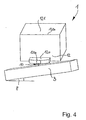
- Fig. 4 shows a front perspective view of cantilever assembly 1, together with a sample 3 that is slightly tilted by an angle ⁇ relative to cantilever 10 and support 12. From Fig. 4 another problem usually encountered in the scanning of samples becomes apparent. This problem is related to the tilted arrangement of sample 3 relative to cantilever 10 and support 12, and will now be explained.
- Cantilever assembly 1 may approach sample 3 from behind as is shown in Fig. 4 .
- Cantilever 10 is attached to support 12 comprising steps'120 and 121.
- step 120 of support 12 (which is that portion of support 12 to which the cantilever is attached) has a recessed shape, in the shown embodiment a partly-octagonal shape.
- the said partly-octagonal shape narrows in the direction towards cantilever 10.
- step 120 is advantageous in that it is on one hand sufficiently stiff (since step 120 has sufficient mass) in order to form a rigid support for cantilever 10.
- the recessed step 120 allows for a certain tilt of sample 3 relative to support 12 or step 120, respectively, so that during approaching the sample 3 a collision between sample 3 and support 12 or step 120, respectively, is unlikely to occur.
Landscapes
- Physics & Mathematics (AREA)
- Health & Medical Sciences (AREA)
- General Health & Medical Sciences (AREA)
- General Physics & Mathematics (AREA)
- Nuclear Medicine, Radiotherapy & Molecular Imaging (AREA)
- Radiology & Medical Imaging (AREA)
- Chemical & Material Sciences (AREA)
- Engineering & Computer Science (AREA)
- Nanotechnology (AREA)
- Analytical Chemistry (AREA)
- Crystallography & Structural Chemistry (AREA)
- Length Measuring Devices With Unspecified Measuring Means (AREA)
- Length Measuring Devices By Optical Means (AREA)
- Automatic Analysis And Handling Materials Therefor (AREA)
- Devices For Use In Laboratory Experiments (AREA)
Abstract
Description
- The invention relates to a process of manufacturing a cantilever assembly for scanning a sample.
- In atomic force microscopy (AFM) or scanning force microscopy (SFM), locally distributed small forces are to be measured in order to obtain an image of a sample. This is done with the aid of a cantilever, which is moved across the sample. That end of the cantilever that is remote from the tip is attached to a rigid support, which has a large mass compared to that of the cantilever. Upon movement of the cantilever across the sample, the forces acting on the cantilever tip result in deflection of the cantilever. The deflection is detected and processed, and together with an information about the respective position of the tip relative to the sample an image of the sample can be obtained.
- Because of the thermal noise of the cantilever, a high resonance frequency and a low stiffness of the cantilever are desirable. Thus, the thermal noise is reduced and the sensitivity is enhanced. High sensitivities of the cantilevers are required for obtaining a high quality image. A high resonance frequency of the cantilever is furthermore advantageous with respect to dynamic measurements in which high scanning speeds are desired. Since the resonance frequency of the cantilever increases with an increasing stiffness and a decreasing mass of the cantilever and at the same time a large ratio of resonance frequency to stiffness is desired to increase cantilever sensitivity, cantilevers having little mass are preferred. This calls for small cantilevers having little length, width and thickness.
- In addition, a high quality factor of the respective cantilever increases its sensitivity. The quality factor is representative of the attenuation of a given excitation: the higher the quality factor, the longer the duration of the oscillation caused by a given excitation (i.e. the lower the attenuation).
- Small cantilevers have been suggested which have been made from silicon-nitride. However, the quality factor of cantilevers made from silicon-nitride is intrinsically low and accordingly, their sensitivity is limited. Cantilevers made from pure silicon offer enhanced sensitivity due to a higher quality factor of pure silicon.
- As already outlined, the deflection of the cantilever tip as well as the exact position of the tip relative to the sample must be exactly known at any time in order to obtain a high quality image of the sample. For that reason, typically optical tracking of the position of the cantilever tip is performed. This is usually done with the aid of a deflection sensor which receives light that has been reflected from the back side of the cantilever tip. In order to get more light reflected, the back side is typically coated with a high reflectance metal film compared to pure silicon, e.g. a gold film. However, coating the small cantilever with a gold film over a large area and in particular up to the support chip results in considerable decrease of the quality factor and thus results in considerably lower sensitivity.
- Gold coatings may be applied through a mask which allows gold evaporated from a source only to impinge on the back side of the cantilever through a well-defined opening in the mask. The macroscopic dimensions of the support chip necessary for high rigidity and for practical use make it practically impossible to deposit the gold in an area having well-defined sharp boundaries, since the mask cannot be positioned in sufficiently close proximity to the back side of the cantilever tip. Rather, boundaries having considerable extensions are resulting from application of conventional masking techniques. Also, the smaller the dimensions of the cantilevers are, the more the alignment of a separate mask becomes difficult, and with regard to very small cantilevers in the micron-size, deposition of a gold film through a separate mask is not feasible.
-
US 5,245,863 discloses an atomic probe microscope having a cantilever assembly which comprises a cantilever with a length of 500 µm to 2000 µm, a thickness of 5 µm, and a width of 200 µm. A mirror is formed at the back side of cantilever by depositing Au or Al. - Viani et al., Small Cantilevers for Force Spectroscopy of Single Molecules, Journal of Applied Physics, Vol. 86, No. 4, 1999, page 2258 discloses to fabricate an atomic force microscope cantilever having a gold reflector pad formed on its front end, the cantilever being 9 µm to 5.0 µm long, 3 µm to 5 µm wide, and 86 nm thick, and the gold pad having nominal thickness of 100 nm.
-
WO 02/080186 A1 - It is the technical problem underlying the invention to provide a process of manufacturing a cantilever assembly, which is capable to reduce or avoid the inconveniencies of the prior art mentioned above.
- The invention solves this problem by providing a manufacturing process having the features of claim 1. Advantageous embodiments of the invention are mentioned in the dependent claims, the wording of which is herewith incorporated into the description by reference to avoid unnecessary text repetition.
- In the cantilever manufactured by the process according to the invention, the"penumbra" (the slope) at the area covered with the high reflectance material (e. g. gold) has an extension towards the support that is equal to or smaller than the extension of the area itself. More preferably, the ratio of c/Δc is equal to or greater than two, defining an even sharper slope. The cantilever of such a cantilever assembly may thus have a high quality factor even when the cantilever is small. With regard to a high quality factor, the area on the back side of the cantilever tip should not have a large extension and should also have a sharp boundary, since covering a large portion of the back side of the cantilever results in a significant decrease of the quality factor of the cantilever and thus results in considerably decreased sensitivity.
- As already mentioned, this may be particularly advantageous - but not limited to - small cantilevers. Small cantilevers may be cantilevers, wherein the length of the cantilever is in the range of 1 µm to 100 µm, in particular in the range of 3 µm to 20 µm, and wherein the extension c of the area covered by the high reflectance material is in the range of 0.5 µm to 10 µm, in particular in the range of 1 µm to 6 µm.
- In an embodiment of the cantilever assembly manufactured by the process according to the invention, the support is provided with a sharp edge that is located at a distance from the back side of the cantilever tip. This distance is determined such that during application of the high reflectance material the area on the back side of the cantilever tip and the sloping boundary are formed. The location of the sharp edge is thus used to determine the extension of the area of the high reflectance material on the back side of the cantilever as well as the extension of the sloping boundary. It is thus possible on one hand to arrange the "mask" (the edge) in close proximity to the area to which the high reflectance material (e.g. gold) is to be applied. On the other hand, no separate mask is needed, since the mask is formed by a part of the support thus eliminating the problems encountered with the alignment of a separate mask. Using dry-etching techniques it is possible to produce such sharp edges with the required accuracy at the determined location.
- In an advantageous embodiment of the cantilever assembly manufactured by the process according to the instant invention, the support further comprises a guidance and calibration structure for guiding and calibrating an optical tracking system in focusing on the area covered by the high reflectance material.
- When AFM is started, first of all the optical tracking system must "find" the cantilever tip. Also, it must be known which amount of movement of the optical system corresponds to which distance. In order to facilitate this, the aforementioned embodiment is advantageous, since in case no guidance and calibration structure were present, the three-dimensional space must otherwise be searched in fine steps in order to find the cantilever tip. However, searching the cantilever tip in this manner takes considerable time. The guiding and calibrations structure simplifies finding the cantilever tip, since it provides information as to where to find the cantilever tip, so that finally only a small segment of the three-dimensional space must be searched in fine steps for finding the exact position of the cantilever tip.
- In a further embodiment of the cantilever assembly manufactured by the process according to the instant invention, that portion of the support to which the cantilever is attached has recessed shape, in particular a partly-octagonal shape, the said recessed or partly-octagonal shape narrowing in the direction towards the cantilever. A thus shaped portion of the support is sufficiently stiff on one hand while at the same time - due to its "narrowed" shape - it allows that a sample may be arranged tilted within a certain range relative to the cantilever or the support, respectively, without provoking a collision between the support and the sample during approaching the sample for a scan.
- In still a further embodiment of the cantilever assembly manufactured by the process according to the instant invention, the cantilever comprises a step-like portion which is arranged near that end of the cantilever which is attached to the support. At the step-like portion the thickness of the cantilever on the front side of the cantilever (i.e. that side of the cantilever facing the sample) is substantially increased. The step-like portion enables to very precisely define the length of the cantilever, since the length from the step towards the cantilever tip defines the length of the cantilever. The step can be manufactured with etching techniques (e.g. wet etching techniques or dry etching techniques) applied from the front side of the cantilever. This is particularly advantageous with respect to manufacture of the cantilever assemblies from so-called "silicon on oxide" wafers, as will be explained in more detail below.
- In a still further embodiment of the cantilever manufactured by the process according to the instant invention, the support comprises at least two steps, each step being provided with an edge. The edge of the first step of the support (that edge forming the "mask") is located the said predetermined distance from the back side of the cantilever tip, while the edge of the second step is located such that it does not obstruct application of the high reflectance material.
- The two-step embodiment is advantageous in that the first step and in particular the edge of the first step is located relatively close to the back side of the cantilever tip at the above-mentioned predetermined distance. When the high reflectance material, e.g. gold, is deposited on the back side of the cantilever through evaporation of the high reflectance material from a source, it must be ensured, that the edge of the second step does not obstruct application of the high reflectance material. Otherwise, the edge of the second step would define the boundary of the area covered by the high reflectance material, and since the edge of the second step is located too far away from the back side of the cantilever tip, a well-defined sharp boundary of the covered area as specified above may not be manufactured.
- A further aspect of the instant invention deals with a process for manufacturing a cantilever assembly as described before. This process comprises applying from a source of a high reflectance material the area of the high reflectance material and the sloping boundary to the back side of the cantilever tip. The process further comprises using a sharp edge of the support of the cantilever assembly in order to limit the extensions of the area and of the boundary towards the support. While not being limited to small cantilevers, this process is particularly advantageous with regard to small cantilevers, since no separate mask is needed which must be precisely arranged. Rather, the edge functions as the "mask" and can be positioned sufficiently close to the cantilever tip in case of small cantilevers.
- In an embodiment of the process according to the instant invention, the edge of the support is located at a distance from the area on the back side of cantilever tip. The source of the high reflectance material is also arranged at a distance from the edge of the support and has an opening having a diameter, through which the high reflectance material is applied. The distance of the edge of the support from the area on the back side of cantilever tip and the distance from the source to the edge of the support are determined such, that the condition

- Δc
- denotes the extension of the boundary of the area of the high reflectance material towards the support
- 1
- denotes the distance of the edge of the support from the area of the high reflectance material,
- d
- denotes the diameter of the opening of the source through which the high reflectance material is applied,
- L
- denotes the distance between the source and the edge of the support.
- Further advantageous aspects of the process according to the instant invention will become apparent from the following detailed description of an embodiment of the cantilever assembly with the aid of the drawings in which:
- Fig. 1
- shows a longitudinal section through an embodiment of the cantilever assembly manufactured by the process according to the instant invention,
- Fig. 2
- shows a perspective view of the embodiment of the cantilever assembly of
Fig. 1 , - Fig. 3
- shows essentially the longitudinal section through the embodiment of the cantilever assembly of
Fig. 1 together with a schematic representation of an aperture angle of the optical tracking system - Fig. 4
- shows a front perspective view of the embodiment of the cantilever assembly of
Fig.1 , with a sample tilted relative to the cantilever. - One embodiment of the cantilever assembly 1 manufactured by the process in accordance with the instant invention, as shown in
Fig. 1 , comprises acantilever 10 having acantilever tip 11 for scanning a sample (not shown).Cantilever 10 is attached to asupport 12, e.g. a chip. The embodiment shown is made from a so-called "silicon-on-oxide" wafer, that is to say, it is made from a wafer comprising three layers, a pure silicon layer followed by a silicon oxide layer which is again followed by a pure silicon layer. These layers are indicated by Si and SiO2 respectively inFig. 1 . - On the backside of
cantilever 10 in the region of cantilever tip 11 (this region is in the following called "the back side of cantilever tip") anarea 110 consisting of a high reflectance material, e.g. gold, is provided. A high reflectance material is a material having a higher reflectance compared to pure silicon. Thisarea 110 is sharply bounded on three sides, sincecantilever 10 ends on these three sides. On the fourth side, i.e. in the direction towardssupport 12,area 110 has aboundary 111 that slopes towards the back side ofcantilever 10. -
Area 110 has an extension c in the direction towardssupport 12. As has already been outlined,boundary 111 should be comparatively sharp, that is to say it should not have an extension Δc towardssupport 12 that is larger than extension c ofarea 110. This can be achieved with the aid of a specific shape ofsupport 12, as will be explained in more detail below. -
Support 12 has a stepped structure and comprises in the embodiment shown inFig. 1 twosteps first step 120 is provided with asharp edge 120a which is located a distance 1 from the backside ofcantilever tip 11. Thesecond step 121 is provided with a furthersharp edge 121a, which is located such that it does not obstruct application of the high reflectance material. - For the sake of better understanding how the comparatively
sharp boundary 111 can be manufactured even for very small cantilevers in the range of 3 µm to 20 µm and forareas 110 in the range of 0.5 µm to 6 µm, let us assume, that the high reflectance material, e.g. gold, is to be applied to the back side ofcantilever tip 11 from an evaporation source S that is arranged relative to the back side ofcantilever 10 or to the back side ofcantilever tip 11 under a redefined angle α. A typical range for angle α is up to 15°. Also, the distance 1+L from the aperture of evaporation source S to the back side ofcantilever tip 11 is specified for a given evaporation source, typically this distance is within some ten centimeters. - As can be seen from
Fig. 1 , distance 1 denotes the distance fromedge 120a to the back side ofcantilever tip 11, while distance L denotes the distance fromedge 120a to the aperture of evaporation source S. Evaporation source S has a well-defined diameter d of its aperture through which the gold is evaporated. - From the geometry of the arrangement shown in
Fig. 1 , the following equation can be derived: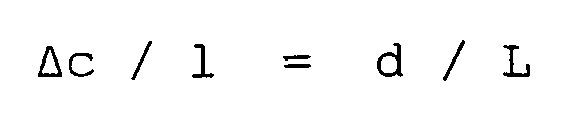
- As already outlined, the ratio of extension c of
area 110 to extension Δc ofboundary 111 must be equal to or greater than one, more preferably equal to or greater than two. From the condition
- follows, that for determination of the distance 1 of the
area 110 fromedge 120a the following condition applies: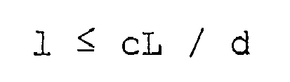
- Just by way of example, if the extension c of
area 110 is 4 µm, the distance L is 20 cm (it is in the range of some 10 centimeters, see above), and the diameter d of the aperture of evaporation source S is 1 cm (see also above), then a distance 1 results being equal to or smaller than 80 µm. - As can be seen from
Fig. 1 ,edge 120a serves for limiting the extension Δc of slopedboundary 111 ofarea 110 on the back side ofcantilever tip 11 in the direction towardssupport 12. With regard to the other three boundaries ofarea 110, the back side ofcantilever tip 11 is covered up to the respective edge of the back side ofcantilever tip 11. - When using the so-called "silicon-on-oxide" wafers, the SiO2-layer between the two pure Si-layers forms a stop for an etching process. However, in order to completely expose
cantilever 10, the SiO2-layer has also been removed after the etching process described above, as can be seen inFig. 1 . Since the mechanical properties of SiO2 are considerably different from those of Si,cantilever 10 would not be optimally attached to support 12, since two materials having different mechanical properties (e.g. thermal expansion coefficients) are abutting against each other at the attachment location. This would result in a reduced quality factor and accordingly in a reduced sensitivity ofcantilever 10, if no additional measures were taken. - In order maintain the high quality factor of
cantilever 10,cantilever 10 is provided with a step-like portion 100 which is arranged near that end ofcantilever 10 which is attached to support 12. Step-like portion 100 is arranged a small distance away from the attachment location. At step-like portion 100, the thickness ofcantilever 10 substantially increases on the front side of cantilever 10 - i.e. on that side ofcantilever 10 facing downwards inFig.1 . By providing step-like portion 100 the length ofcantilever 10 is well-defined, since after having increased its thickness, that portion with the substantially increased thickness already functions as a support. Accordingly; the flexible part ofcantilever 10 has a well-defined length, and in addition the attachment of the flexible part ofcantilever 10 to the massive "support" is executed in the same material (silicon), thus avoiding a decrease of the quality factor. - Referring now to
Fig. 2 , cantilever assembly 1 is shown in a perspective view, so that a more detailed impression of the shapes of the twosteps step 120 will be explained in further detail below with respect toFig. 4 .Fig. 2 further shows an embodiment of a guidance andcalibration structure 123 comprising - by way of example - twogrooves 123a and 123b extending symmetrically and parallel to continuedlongitudinal axis 101 ofcantilever 10. In addition, guidance andcalibration structure 123 comprises arecess 123c or pit having a well-defined length and depth, which is arranged on the continuedlongitudinal axis 101 ofcantilever 10. Guidance andcalibration structure 123 is intended to help in guiding and calibrating the optical tracking system (e.g. during positioning of the deflection sensor), since firstly the optical tracking system must "find" the cantilever tip. -
Grooves 123a and 123b as well asrecess 123 and their edges are very precisely manufactured at very precise locations. Accordingly, in a first step optical tracking system focuses on the upper surface ofstep 121 in order to start a guiding and calibration run. The following explanation offers one out of a number of possibilities how such a guiding and calibration run of the optical system may look like. - After having focused on the upper surface of
step 121, the displacement units of the optical tracking system - which are schematically represented by three-dimensional arrow arrangement 21 inFig. 2 - move the optical tracking system, which is schematically represented throughbeam 20 inFig. 2 , in a direction perpendicular to continuedlongitudinal axis 101 untilbeam 20 reaches the edge of a groove. For example, the displacement units of the optical tracking system firstly move optical tracking system in the direction ofarrow 210 until it reaches the inner edge ofgroove 123a. The inner edge ofgroove 123a is sensed - for example - by a change in intensity of the reflected light. The displacement units then move optical tracking system in the direction ofarrow 211 until it reaches the inner edge of groove 123b. Once it has detected the inner edge of groove 123b, optical tracking system knows, that continuedlongitudinal axis 101 must be located half-way between the two detected edges because of the symmetrical arrangement ofgrooves 123a and 123b with respect to continuedlongitudinal axis 101. Also, since optical tracking system has counted the number of steps a stepper motor driving the displacement units has needed to move optical system between the inner edges ofgrooves 123a and 123b, and because the distance between the inner edges ofgrooves 123a and 123b is precisely known, optical tracking system exactly knows the distance to which one step of the stepper motor corresponds in the direction ofarrows - The displacement units now move optical tracking system (i.e. beam 20) back to continued
longitudinal axis 101 and subsequently continues to move optical tracking system in a direction perpendicularly toarrows arrow 212 untilbeam 20 reaches the inner edge ofrecess 123c. The displacement units continue to move optical tracking system acrossrecess 123c in the direction of continuedlongitudinal axis 101 untilbeam 20 reaches the outer edge ofrecess 123c. Again, optical tracking system counts the number of steps needed to movebeam 20 from the inner edge ofrecess 123c to the outer edge ofrecess 123c. Since the distance between inner and outer edge ofrecess 123c is precisely known, the optical tracking system now knows the distance to which one step of the stepper motor corresponds in the direction ofarrow 212. Optical tracking system is now calibrated in the plane of upper surface of step 120b and can be guided on continuedlongitudinal axis 101. -
Recess 123c can also be used for calibration of the optical tracking system with respect to depth, sincerecess 123c has a precisely defined depth, as outlined above. Accordingly, the displacement units can move optical tracking system back overrecess 123c so thatbeam 20 is out of focus. Subsequently, the displacement units move optical tracking system in the direction ofarrow 213 untilbeam 20 is focused on the bottom surface ofrecess 123c, which can be detected - for example - by detecting the maximum intensity of the reflected light. Again, the optical tracking system counts the number of steps of the stepper motor required between the position in whichbeam 20 is focused on the upper surface ofstep 121 and the position in whichbeam 20 is focused on the bottom surface ofrecess 123c. Since the depth ofrecess 123c is precisely known, optical tracking system now knows the distance to which one step of the stepper motor corresponds in the direction ofarrow 213. - Optical tracking system is now moved back to focus on the upper surface of
step 121, and can now be moved along longitudinal axis untilbeam 20passes edge 121a ofstep 121. Having passededge 121a, optical tracking system is moved downwardly towardsstep 120, untilbeam 20 is focused to the upper surface ofstep 120. Then optical tracking system can be moved along continuedlongitudinal axis 101 untilbeam 20passes edge 120a ofstep 120. Having passededge 120a ofstep 120, optical tracking system is moved downwardly towards the back side ofcantilever 10, until it is focused on the back side ofcantilever 10. Movement of optical tracking system is then continued untilbeam 20 impinges onarea 110, which can be identified by the increasing intensity of the reflected light. - In order to substantially accelerate guiding and focusing the optical tracking system to the back side of
cantilever tip 11 after calibration, the distance between inner and/or outer edge ofrecess 123c andedge 121a ofstep 121 is known, as well as the distance between upper surface ofstep 121 and upper surface ofstep 120. Finally, the length ofstep 120 is also known, as well as the distance between the upper surface ofstep 120 and the back side ofcantilever 10. Finally, the length ofcantilever 10 is known, so that optical tracking system can be quickly guided and focused to a target point in the three-dimensional space, which is located at least in relatively close vicinity ofarea 110. The final exact positioning and focusing onarea 110 can then be performed in a comparatively short time, since optical tracking system must only "search" in a very small section of the three-dimensional space, since it can be quickly guided to a point in the three-dimensional space, which is located at least in close vicinity ofarea 110. As outlined above, the calibration structure shown inFig. 2 has only been described by way of example and other suitable calibration structures can be used as well. - Turning now to
Fig. 3 , which shows essentially a longitudinal section through the embodiment of the cantilever assembly shown inFig. 1 , but in addition represents the angular aperture β of an optical tracking system having a high numerical aperture. The shape of cantilever assembly 1 is not in contrast with a high numerical aperture of the optical tracking system. This is advantageous with respect to obtaining a small focus spot (typically < 5µm) onarea 110 on the back side ofcantilever tip 11. The higher the numerical aperture that can be used the more precise the focusing and the higher the quality of the image from the sample. An aperture β of greater than 30° is particularly advantageous. -
Fig. 4 shows a front perspective view of cantilever assembly 1, together with asample 3 that is slightly tilted by an angle γ relative to cantilever 10 andsupport 12. FromFig. 4 another problem usually encountered in the scanning of samples becomes apparent. This problem is related to the tilted arrangement ofsample 3 relative to cantilever 10 andsupport 12, and will now be explained. Cantilever assembly 1 may approachsample 3 from behind as is shown inFig. 4 .Cantilever 10 is attached to support 12 comprising steps'120 and 121. In order now to avoid a collision betweensupport 12 and sample 3 (or more precisely betweenstep 120 of the support and sample 3) during approachingsample 3, step 120 of support 12 (which is that portion ofsupport 12 to which the cantilever is attached) has a recessed shape, in the shown embodiment a partly-octagonal shape. The said partly-octagonal shape narrows in the direction towardscantilever 10. - The recessed partly-octagonal shape of
step 120 is advantageous in that it is on one hand sufficiently stiff (sincestep 120 has sufficient mass) in order to form a rigid support forcantilever 10. On the other hand, the recessedstep 120 allows for a certain tilt ofsample 3 relative to support 12 orstep 120, respectively, so that during approaching the sample 3 a collision betweensample 3 andsupport 12 orstep 120, respectively, is unlikely to occur.
Claims (6)
- A process for manufacturing a cantilever assembly (1) for scanning a sample comprising a cantilever (10) having a cantilever tip (11), the cantilever (10) being mounted to a rigid support (12, 120, 121) and being provided on its back side facing away from the sample (3) with an area (110) of a high reflectance material, this area having a boundary (111) sloping towards the support (12), wherein the extensions (c, Δc) of the area (110) and of the boundary (111) towards the support fulfil the condition

wherein c denotes the extension of the area (110) of the high reflectance material in the direction towards the support (12), and Δc denotes the extension of the sloped boundary (111) of the area (110) of the high reflectance material in the direction towards the support (12),
the process comprising:applying from a source (S) of a high reflectance material the area (110) of the high reflectance material and the sloping boundary (111) to the back side of the cantilever tip (11), wherein a sharp edge (120a) of the support (12) of the cantilever assembly (1) is used in order to limit the extensions (c, Δc) of the area (110) and of the boundary (111) towards the support (12). - The process according to claim 1, wherein the edge (120a) of the support (12) is located at a distance (1) from the area (110) on the back side of cantilever tip (11), wherein the source (S) of the high reflectance material is arranged at a distance (L) from the edge (120a) of the support (12) and has an opening having a diameter (d), through which the high reflectance material is applied, and wherein the distance (I) from the area (110) on the back side of cantilever tip (11) and the edge (120a) of the support (12) and the distance (L) from the source to the edge (120a) of the support (12) are determined such that

wherein
I denotes the distance of the edge (120a) of the support (12) from the area (110) of the high reflectance material,
d denotes the diameter of the opening of the source (S) through which the high reflectance material is applied, and
L denotes the distance between the source (S) and the edge (120a) of the support (12). - The process according to claim 1 or 2, wherein the length of the cantilever (10) is in the range of 1 µm to 100 µm, in particular in the range of 3 µm to 20 µm, and wherein the extension (c) of the area (110) of the high reflectance material towards the support (12) is in the range of 0.5 µm to 10 µm, in particular in the range of 1 µm to 6 µm.
- The process according to any one of the preceding claims, wherein that portion (120) of the support (12), to which the cantilever (10) is attached, is formed to have a recessed shape, preferably a partly-octagonal shape, said recessed shape narrowing in the direction towards the cantilever (10).
- The process according to any one of the preceding claims, wherein the cantilever (10) is formed to comprise a step-like portion (100) which is arranged near that end of the cantilever (10) which is attached to the support (12, 120), said step-like portion (100) substantially increasing the thickness of the cantilever (10) on the front side of the cantilever (10).
- The process according to any one of the preceding claims, wherein the support (12) is formed to comprise at least two steps, a first one (120) providing said sharp edge (120a) and a second one providing another edge (121a), wherein the edge (120a) of the first step (120) is located such that during application of the high reflectance material the area (110) on the back side of the cantilever tip (11) and the sloping boundary (111) are formed and wherein the edge (121a) of the second step (121) is located such that it does not obstruct the application of the high reflectance material.
Priority Applications (3)
| Application Number | Priority Date | Filing Date | Title |
|---|---|---|---|
| EP04798772A EP1680788B1 (en) | 2003-11-04 | 2004-11-04 | Cantilever assembly |
| EP08003535A EP1993102A1 (en) | 2003-11-04 | 2004-11-04 | Cantilever assembly and process of manufacturing the same |
| EP08003536A EP1993103A1 (en) | 2003-11-04 | 2004-11-04 | Cantilever assembly and process of manufacturing the same |
Applications Claiming Priority (3)
| Application Number | Priority Date | Filing Date | Title |
|---|---|---|---|
| EP03025187A EP1530220A1 (en) | 2003-11-04 | 2003-11-04 | Cantilever assembly |
| EP04798772A EP1680788B1 (en) | 2003-11-04 | 2004-11-04 | Cantilever assembly |
| PCT/IB2004/003599 WO2005043551A1 (en) | 2003-11-04 | 2004-11-04 | Cantilever assembly |
Related Child Applications (4)
| Application Number | Title | Priority Date | Filing Date |
|---|---|---|---|
| EP08003536A Division EP1993103A1 (en) | 2003-11-04 | 2004-11-04 | Cantilever assembly and process of manufacturing the same |
| EP08003535A Division EP1993102A1 (en) | 2003-11-04 | 2004-11-04 | Cantilever assembly and process of manufacturing the same |
| EP08003536.3 Division-Into | 2008-02-27 | ||
| EP08003535.5 Division-Into | 2008-02-27 |
Publications (2)
| Publication Number | Publication Date |
|---|---|
| EP1680788A1 EP1680788A1 (en) | 2006-07-19 |
| EP1680788B1 true EP1680788B1 (en) | 2011-09-14 |
Family
ID=34429250
Family Applications (4)
| Application Number | Title | Priority Date | Filing Date |
|---|---|---|---|
| EP03025187A Withdrawn EP1530220A1 (en) | 2003-11-04 | 2003-11-04 | Cantilever assembly |
| EP08003535A Ceased EP1993102A1 (en) | 2003-11-04 | 2004-11-04 | Cantilever assembly and process of manufacturing the same |
| EP08003536A Ceased EP1993103A1 (en) | 2003-11-04 | 2004-11-04 | Cantilever assembly and process of manufacturing the same |
| EP04798772A Expired - Lifetime EP1680788B1 (en) | 2003-11-04 | 2004-11-04 | Cantilever assembly |
Family Applications Before (3)
| Application Number | Title | Priority Date | Filing Date |
|---|---|---|---|
| EP03025187A Withdrawn EP1530220A1 (en) | 2003-11-04 | 2003-11-04 | Cantilever assembly |
| EP08003535A Ceased EP1993102A1 (en) | 2003-11-04 | 2004-11-04 | Cantilever assembly and process of manufacturing the same |
| EP08003536A Ceased EP1993103A1 (en) | 2003-11-04 | 2004-11-04 | Cantilever assembly and process of manufacturing the same |
Country Status (6)
| Country | Link |
|---|---|
| US (1) | US8109135B2 (en) |
| EP (4) | EP1530220A1 (en) |
| JP (1) | JP4839220B2 (en) |
| CN (2) | CN1871665B (en) |
| AT (1) | ATE524744T1 (en) |
| WO (1) | WO2005043551A1 (en) |
Families Citing this family (3)
| Publication number | Priority date | Publication date | Assignee | Title |
|---|---|---|---|---|
| EP1530220A1 (en) * | 2003-11-04 | 2005-05-11 | SwissProbe AG | Cantilever assembly |
| EP2657710A1 (en) * | 2012-04-25 | 2013-10-30 | Commissariat A L'energie Atomique Et Aux Energies Alternatives | Characterization structure for an atomic force microscope tip |
| EP3591410A1 (en) * | 2018-07-06 | 2020-01-08 | Nederlandse Organisatie voor toegepast- natuurwetenschappelijk onderzoek TNO | Probe chip, scan head, scanning probe microscopy device and use of a probe chip |
Family Cites Families (23)
| Publication number | Priority date | Publication date | Assignee | Title |
|---|---|---|---|---|
| JP2945725B2 (en) * | 1990-07-20 | 1999-09-06 | オリンパス光学工業株式会社 | Atomic probe microscope |
| JPH0470506A (en) * | 1990-07-11 | 1992-03-05 | Olympus Optical Co Ltd | Atomic probe microscope |
| US5245863A (en) * | 1990-07-11 | 1993-09-21 | Olympus Optical Co., Ltd. | Atomic probe microscope |
| JP2967308B2 (en) | 1991-09-09 | 1999-10-25 | キヤノン株式会社 | Micro cantilever probe, method of manufacturing the same, surface observation device and information processing device provided with the same |
| US5319961A (en) * | 1991-09-17 | 1994-06-14 | Olympus Optical Co., Ltd. | Cantilever chip for use in scanning probe microscope |
| JPH08297129A (en) | 1995-04-26 | 1996-11-12 | Nikon Corp | Cantilever for atomic force microscope and method of manufacturing the same |
| JPH08313541A (en) * | 1995-05-16 | 1996-11-29 | Olympus Optical Co Ltd | Cantilever for scanning probe microscope and its manufacture |
| JPH09105755A (en) | 1995-10-11 | 1997-04-22 | Olympus Optical Co Ltd | Afm cantilever and its manufacture |
| JPH09159680A (en) | 1995-12-05 | 1997-06-20 | Nikon Corp | Cantilever holder, heating device using the same, and heating / shape measuring device using the same |
| JPH09196933A (en) | 1996-01-19 | 1997-07-31 | Canon Inc | PROBE, METHOD FOR PRODUCING PROBE, PROBE UNIT, AND INFORMATION RECORDING / REPRODUCING DEVICE USING THE SAME |
| JP3599880B2 (en) | 1996-03-12 | 2004-12-08 | オリンパス株式会社 | Cantilever tip |
| JPH09304410A (en) | 1996-05-20 | 1997-11-28 | Olympus Optical Co Ltd | Afm cantilever |
| US5982009A (en) | 1997-03-01 | 1999-11-09 | Korea Advanced Institute Of Science & Technology | Integrated device of cantilever and light source |
| JP3222410B2 (en) | 1997-09-29 | 2001-10-29 | セイコーインスツルメンツ株式会社 | Cantilever unit, its holder, and scanning probe microscope equipped therewith |
| JP3309816B2 (en) * | 1998-01-22 | 2002-07-29 | 松下電器産業株式会社 | Micro surface shape measuring device and stylus manufacturing method |
| JP2001188035A (en) | 1999-03-17 | 2001-07-10 | Seiko Instruments Inc | Scanning probe microscope |
| JP2002116132A (en) | 2000-10-04 | 2002-04-19 | Canon Inc | Signal detection apparatus, scanning atomic force microscope constructed of it, and signal detection method |
| JP2002162335A (en) * | 2000-11-26 | 2002-06-07 | Yoshikazu Nakayama | Cantilever for vertical scanning microscope and probe for vertical scanning microscope using the same |
| WO2002080186A1 (en) * | 2001-03-30 | 2002-10-10 | Johns Hopkins University | Afm cantilevers and methods for making and using same |
| JP4646049B2 (en) * | 2001-07-30 | 2011-03-09 | 国立大学法人金沢大学 | Scanning probe microscope |
| US7313828B2 (en) * | 2001-09-04 | 2007-12-25 | Nokia Corporation | Method and apparatus for protecting software against unauthorized use |
| JP2004198134A (en) * | 2002-12-16 | 2004-07-15 | Olympus Corp | Cantilever for scanning type probe microscope |
| EP1530220A1 (en) * | 2003-11-04 | 2005-05-11 | SwissProbe AG | Cantilever assembly |
-
2003
- 2003-11-04 EP EP03025187A patent/EP1530220A1/en not_active Withdrawn
-
2004
- 2004-11-04 EP EP08003535A patent/EP1993102A1/en not_active Ceased
- 2004-11-04 AT AT04798772T patent/ATE524744T1/en not_active IP Right Cessation
- 2004-11-04 WO PCT/IB2004/003599 patent/WO2005043551A1/en not_active Ceased
- 2004-11-04 JP JP2006537478A patent/JP4839220B2/en not_active Expired - Fee Related
- 2004-11-04 EP EP08003536A patent/EP1993103A1/en not_active Ceased
- 2004-11-04 EP EP04798772A patent/EP1680788B1/en not_active Expired - Lifetime
- 2004-11-04 US US10/595,690 patent/US8109135B2/en not_active Expired - Fee Related
- 2004-11-04 CN CN200480030683XA patent/CN1871665B/en not_active Expired - Fee Related
- 2004-11-04 CN CNA200810094453XA patent/CN101286373A/en active Pending
Also Published As
| Publication number | Publication date |
|---|---|
| CN101286373A (en) | 2008-10-15 |
| EP1680788A1 (en) | 2006-07-19 |
| WO2005043551A1 (en) | 2005-05-12 |
| EP1993102A1 (en) | 2008-11-19 |
| CN1871665B (en) | 2011-09-21 |
| JP2007510896A (en) | 2007-04-26 |
| ATE524744T1 (en) | 2011-09-15 |
| US20070271996A1 (en) | 2007-11-29 |
| EP1993103A1 (en) | 2008-11-19 |
| EP1530220A1 (en) | 2005-05-11 |
| CN1871665A (en) | 2006-11-29 |
| US8109135B2 (en) | 2012-02-07 |
| JP4839220B2 (en) | 2011-12-21 |
Similar Documents
| Publication | Publication Date | Title |
|---|---|---|
| JP4472863B2 (en) | Near-field optical probe and near-field optical device using the near-field optical probe | |
| EP0444697A2 (en) | Atomic probe microscope and cantilever unit for use in the microscope | |
| JP3174705B2 (en) | Manufacturing method of fiber probe device | |
| US6104030A (en) | Optical probe having tapered wave guide and scanning near-field optical microscope utilizing optical probe | |
| US8857247B2 (en) | Probe for a scanning probe microscope and method of manufacture | |
| US7265057B2 (en) | 3D lithography with laser beam writer for making hybrid surfaces | |
| EP1993103A1 (en) | Cantilever assembly and process of manufacturing the same | |
| US8011016B2 (en) | SPM probe with shortened cantilever | |
| DE102017205528A1 (en) | Apparatus and method for a scanning probe microscope | |
| RU2320034C2 (en) | Probe for scanning probe microscope and method for manufacturing it | |
| US6747265B1 (en) | Optical cantilever having light shielding film and method of fabricating the same | |
| JP2000105184A (en) | Cantilever lever with tall probe for atomic force microscope | |
| JP4751440B2 (en) | Near-field optical probe, manufacturing method thereof, and near-field optical device using the near-field optical probe | |
| JP3764816B2 (en) | Flamingo optical probe, flamingo optical probe manufacturing method, and scanning probe microscope | |
| US20250290950A1 (en) | High Frequency Passivated AFM Cantilever and Method of Fabrication | |
| US11644480B2 (en) | Thermally stable, drift resistant probe for a scanning probe microscope and method of manufacture | |
| KR100465260B1 (en) | Nano-slide integrated nano-probe and manufacture method thereof | |
| JPH10311843A (en) | Cantilever and manufacturing method thereof |
Legal Events
| Date | Code | Title | Description |
|---|---|---|---|
| PUAI | Public reference made under article 153(3) epc to a published international application that has entered the european phase |
Free format text: ORIGINAL CODE: 0009012 |
|
| 17P | Request for examination filed |
Effective date: 20060328 |
|
| AK | Designated contracting states |
Kind code of ref document: A1 Designated state(s): AT BE BG CH CY CZ DE DK EE ES FI FR GB GR HU IE IS IT LI LU MC NL PL PT RO SE SI SK TR |
|
| 17Q | First examination report despatched |
Effective date: 20060810 |
|
| 19U | Interruption of proceedings before grant |
Effective date: 20061031 |
|
| 19W | Proceedings resumed before grant after interruption of proceedings |
Effective date: 20071001 |
|
| RAP1 | Party data changed (applicant data changed or rights of an application transferred) |
Owner name: NANO WORLD AG |
|
| R17C | First examination report despatched (corrected) |
Effective date: 20071001 |
|
| GRAP | Despatch of communication of intention to grant a patent |
Free format text: ORIGINAL CODE: EPIDOSNIGR1 |
|
| REG | Reference to a national code |
Ref country code: DE Ref legal event code: R079 Ref document number: 602004034362 Country of ref document: DE Free format text: PREVIOUS MAIN CLASS: G12B0021020000 Ipc: G01Q0070000000 |
|
| DAX | Request for extension of the european patent (deleted) | ||
| RIC1 | Information provided on ipc code assigned before grant |
Ipc: G01Q 60/38 20100101ALI20110509BHEP Ipc: G01B 11/30 20060101ALI20110509BHEP Ipc: G01B 5/28 20060101ALI20110509BHEP Ipc: G01B 7/34 20060101ALI20110509BHEP Ipc: G01Q 70/00 20100101AFI20110509BHEP |
|
| GRAS | Grant fee paid |
Free format text: ORIGINAL CODE: EPIDOSNIGR3 |
|
| GRAA | (expected) grant |
Free format text: ORIGINAL CODE: 0009210 |
|
| AK | Designated contracting states |
Kind code of ref document: B1 Designated state(s): AT BE BG CH CY CZ DE DK EE ES FI FR GB GR HU IE IS IT LI LU MC NL PL PT RO SE SI SK TR |
|
| REG | Reference to a national code |
Ref country code: CH Ref legal event code: EP |
|
| REG | Reference to a national code |
Ref country code: IE Ref legal event code: FG4D |
|
| REG | Reference to a national code |
Ref country code: DE Ref legal event code: R096 Ref document number: 602004034362 Country of ref document: DE Effective date: 20111110 |
|
| REG | Reference to a national code |
Ref country code: NL Ref legal event code: VDEP Effective date: 20110914 |
|
| PG25 | Lapsed in a contracting state [announced via postgrant information from national office to epo] |
Ref country code: SE Free format text: LAPSE BECAUSE OF FAILURE TO SUBMIT A TRANSLATION OF THE DESCRIPTION OR TO PAY THE FEE WITHIN THE PRESCRIBED TIME-LIMIT Effective date: 20110914 Ref country code: FI Free format text: LAPSE BECAUSE OF FAILURE TO SUBMIT A TRANSLATION OF THE DESCRIPTION OR TO PAY THE FEE WITHIN THE PRESCRIBED TIME-LIMIT Effective date: 20110914 |
|
| PG25 | Lapsed in a contracting state [announced via postgrant information from national office to epo] |
Ref country code: AT Free format text: LAPSE BECAUSE OF FAILURE TO SUBMIT A TRANSLATION OF THE DESCRIPTION OR TO PAY THE FEE WITHIN THE PRESCRIBED TIME-LIMIT Effective date: 20110914 Ref country code: GR Free format text: LAPSE BECAUSE OF FAILURE TO SUBMIT A TRANSLATION OF THE DESCRIPTION OR TO PAY THE FEE WITHIN THE PRESCRIBED TIME-LIMIT Effective date: 20111215 Ref country code: CY Free format text: LAPSE BECAUSE OF FAILURE TO SUBMIT A TRANSLATION OF THE DESCRIPTION OR TO PAY THE FEE WITHIN THE PRESCRIBED TIME-LIMIT Effective date: 20110914 Ref country code: SI Free format text: LAPSE BECAUSE OF FAILURE TO SUBMIT A TRANSLATION OF THE DESCRIPTION OR TO PAY THE FEE WITHIN THE PRESCRIBED TIME-LIMIT Effective date: 20110914 |
|
| REG | Reference to a national code |
Ref country code: AT Ref legal event code: MK05 Ref document number: 524744 Country of ref document: AT Kind code of ref document: T Effective date: 20110914 |
|
| PG25 | Lapsed in a contracting state [announced via postgrant information from national office to epo] |
Ref country code: BE Free format text: LAPSE BECAUSE OF FAILURE TO SUBMIT A TRANSLATION OF THE DESCRIPTION OR TO PAY THE FEE WITHIN THE PRESCRIBED TIME-LIMIT Effective date: 20110914 |
|
| PG25 | Lapsed in a contracting state [announced via postgrant information from national office to epo] |
Ref country code: CZ Free format text: LAPSE BECAUSE OF FAILURE TO SUBMIT A TRANSLATION OF THE DESCRIPTION OR TO PAY THE FEE WITHIN THE PRESCRIBED TIME-LIMIT Effective date: 20110914 Ref country code: IS Free format text: LAPSE BECAUSE OF FAILURE TO SUBMIT A TRANSLATION OF THE DESCRIPTION OR TO PAY THE FEE WITHIN THE PRESCRIBED TIME-LIMIT Effective date: 20120114 Ref country code: SK Free format text: LAPSE BECAUSE OF FAILURE TO SUBMIT A TRANSLATION OF THE DESCRIPTION OR TO PAY THE FEE WITHIN THE PRESCRIBED TIME-LIMIT Effective date: 20110914 |
|
| PG25 | Lapsed in a contracting state [announced via postgrant information from national office to epo] |
Ref country code: NL Free format text: LAPSE BECAUSE OF FAILURE TO SUBMIT A TRANSLATION OF THE DESCRIPTION OR TO PAY THE FEE WITHIN THE PRESCRIBED TIME-LIMIT Effective date: 20110914 Ref country code: EE Free format text: LAPSE BECAUSE OF FAILURE TO SUBMIT A TRANSLATION OF THE DESCRIPTION OR TO PAY THE FEE WITHIN THE PRESCRIBED TIME-LIMIT Effective date: 20110914 Ref country code: PL Free format text: LAPSE BECAUSE OF FAILURE TO SUBMIT A TRANSLATION OF THE DESCRIPTION OR TO PAY THE FEE WITHIN THE PRESCRIBED TIME-LIMIT Effective date: 20110914 Ref country code: IT Free format text: LAPSE BECAUSE OF FAILURE TO SUBMIT A TRANSLATION OF THE DESCRIPTION OR TO PAY THE FEE WITHIN THE PRESCRIBED TIME-LIMIT Effective date: 20110914 Ref country code: RO Free format text: LAPSE BECAUSE OF FAILURE TO SUBMIT A TRANSLATION OF THE DESCRIPTION OR TO PAY THE FEE WITHIN THE PRESCRIBED TIME-LIMIT Effective date: 20110914 Ref country code: PT Free format text: LAPSE BECAUSE OF FAILURE TO SUBMIT A TRANSLATION OF THE DESCRIPTION OR TO PAY THE FEE WITHIN THE PRESCRIBED TIME-LIMIT Effective date: 20120116 |
|
| PG25 | Lapsed in a contracting state [announced via postgrant information from national office to epo] |
Ref country code: MC Free format text: LAPSE BECAUSE OF NON-PAYMENT OF DUE FEES Effective date: 20111130 |
|
| REG | Reference to a national code |
Ref country code: CH Ref legal event code: PL |
|
| PLBE | No opposition filed within time limit |
Free format text: ORIGINAL CODE: 0009261 |
|
| STAA | Information on the status of an ep patent application or granted ep patent |
Free format text: STATUS: NO OPPOSITION FILED WITHIN TIME LIMIT |
|
| PG25 | Lapsed in a contracting state [announced via postgrant information from national office to epo] |
Ref country code: LI Free format text: LAPSE BECAUSE OF NON-PAYMENT OF DUE FEES Effective date: 20111130 Ref country code: CH Free format text: LAPSE BECAUSE OF NON-PAYMENT OF DUE FEES Effective date: 20111130 Ref country code: DK Free format text: LAPSE BECAUSE OF FAILURE TO SUBMIT A TRANSLATION OF THE DESCRIPTION OR TO PAY THE FEE WITHIN THE PRESCRIBED TIME-LIMIT Effective date: 20110914 |
|
| REG | Reference to a national code |
Ref country code: FR Ref legal event code: ST Effective date: 20120731 |
|
| 26N | No opposition filed |
Effective date: 20120615 |
|
| GBPC | Gb: european patent ceased through non-payment of renewal fee |
Effective date: 20111214 |
|
| REG | Reference to a national code |
Ref country code: IE Ref legal event code: MM4A |
|
| REG | Reference to a national code |
Ref country code: DE Ref legal event code: R097 Ref document number: 602004034362 Country of ref document: DE Effective date: 20120615 |
|
| PG25 | Lapsed in a contracting state [announced via postgrant information from national office to epo] |
Ref country code: IE Free format text: LAPSE BECAUSE OF NON-PAYMENT OF DUE FEES Effective date: 20111104 Ref country code: GB Free format text: LAPSE BECAUSE OF NON-PAYMENT OF DUE FEES Effective date: 20111214 |
|
| PG25 | Lapsed in a contracting state [announced via postgrant information from national office to epo] |
Ref country code: FR Free format text: LAPSE BECAUSE OF NON-PAYMENT OF DUE FEES Effective date: 20111130 |
|
| PG25 | Lapsed in a contracting state [announced via postgrant information from national office to epo] |
Ref country code: ES Free format text: LAPSE BECAUSE OF FAILURE TO SUBMIT A TRANSLATION OF THE DESCRIPTION OR TO PAY THE FEE WITHIN THE PRESCRIBED TIME-LIMIT Effective date: 20111225 |
|
| PG25 | Lapsed in a contracting state [announced via postgrant information from national office to epo] |
Ref country code: LU Free format text: LAPSE BECAUSE OF NON-PAYMENT OF DUE FEES Effective date: 20111104 |
|
| PG25 | Lapsed in a contracting state [announced via postgrant information from national office to epo] |
Ref country code: BG Free format text: LAPSE BECAUSE OF FAILURE TO SUBMIT A TRANSLATION OF THE DESCRIPTION OR TO PAY THE FEE WITHIN THE PRESCRIBED TIME-LIMIT Effective date: 20111214 |
|
| PG25 | Lapsed in a contracting state [announced via postgrant information from national office to epo] |
Ref country code: TR Free format text: LAPSE BECAUSE OF FAILURE TO SUBMIT A TRANSLATION OF THE DESCRIPTION OR TO PAY THE FEE WITHIN THE PRESCRIBED TIME-LIMIT Effective date: 20110914 |
|
| PG25 | Lapsed in a contracting state [announced via postgrant information from national office to epo] |
Ref country code: HU Free format text: LAPSE BECAUSE OF FAILURE TO SUBMIT A TRANSLATION OF THE DESCRIPTION OR TO PAY THE FEE WITHIN THE PRESCRIBED TIME-LIMIT Effective date: 20110914 |
|
| PGFP | Annual fee paid to national office [announced via postgrant information from national office to epo] |
Ref country code: DE Payment date: 20151125 Year of fee payment: 12 |
|
| REG | Reference to a national code |
Ref country code: DE Ref legal event code: R119 Ref document number: 602004034362 Country of ref document: DE |
|
| PG25 | Lapsed in a contracting state [announced via postgrant information from national office to epo] |
Ref country code: DE Free format text: LAPSE BECAUSE OF NON-PAYMENT OF DUE FEES Effective date: 20170601 |