EP1677181A2 - Touch panel device - Google Patents
Touch panel device Download PDFInfo
- Publication number
- EP1677181A2 EP1677181A2 EP05028536A EP05028536A EP1677181A2 EP 1677181 A2 EP1677181 A2 EP 1677181A2 EP 05028536 A EP05028536 A EP 05028536A EP 05028536 A EP05028536 A EP 05028536A EP 1677181 A2 EP1677181 A2 EP 1677181A2
- Authority
- EP
- European Patent Office
- Prior art keywords
- acoustic wave
- surface acoustic
- sender
- substrate
- receiver
- Prior art date
- Legal status (The legal status is an assumption and is not a legal conclusion. Google has not performed a legal analysis and makes no representation as to the accuracy of the status listed.)
- Withdrawn
Links
Images


Classifications
-
- G—PHYSICS
- G06—COMPUTING OR CALCULATING; COUNTING
- G06F—ELECTRIC DIGITAL DATA PROCESSING
- G06F3/00—Input arrangements for transferring data to be processed into a form capable of being handled by the computer; Output arrangements for transferring data from processing unit to output unit, e.g. interface arrangements
- G06F3/01—Input arrangements or combined input and output arrangements for interaction between user and computer
- G06F3/03—Arrangements for converting the position or the displacement of a member into a coded form
- G06F3/041—Digitisers, e.g. for touch screens or touch pads, characterised by the transducing means
- G06F3/043—Digitisers, e.g. for touch screens or touch pads, characterised by the transducing means using propagating acoustic waves
- G06F3/0436—Digitisers, e.g. for touch screens or touch pads, characterised by the transducing means using propagating acoustic waves in which generating transducers and detecting transducers are attached to a single acoustic waves transmission substrate
Definitions
- the present invention relates to a touch panel device that detects the position of a contact body on the coordinate system of a contact surface by transmitting surface acoustic wave sent from a sender element and receiving the surface acoustic wave on a receiver element.
- a touch panel device has a configuration wherein the position of a contact body is detected with a touch of the contact body to a contact surface.
- JP-UM-A-61-112444 (Fig. 4) is an example of related art.
- a coordinate detector according to the example JP-UM-A-61-112444 which is used as a touch panel device, has two sender interdigital transducers for excitation purposes and two pairs of interdigital transducers for reception purposes.
- the surface acoustic wave sent from one exciter interdigital transducer is received by one pair of receiver interdigital transducers on the opposite side.
- the surface acoustic wave sent from the other exciter interdigital transducer is received by the other pair of receiver interdigital transducers on the opposite side.
- An advantage of the invention is to provide a touch panel device that requires a less number of receiver elements and therefore achieves the simplification of the configuration.
- a touch panel device includes: a substrate; a first sender element for sending surface acoustic wave, which is placed along a first direction on the substrate; a second sender element for sending surface acoustic wave, which is placed along a second direction, orthogonal to the first direction, on the substrate; a receiver element for receiving the surface acoustic wave from the second sender element, which is placed along the second direction on the substrate while facing the second sender element with an interval in between; and a reflector, which is placed on the substrate, for achieving the receiver element's reception of the surface acoustic wave from the first sender element by reflecting the surface acoustic wave from the first sender element, wherein a position of a contact body touching on a contact surface is detected by transmitting the surface acoustic wave that is sent from the sender element through the contact surface and receiving the surface acoustic wave on the receiver element.
- the first sender element is placed along the first direction on the substrate and sends surface acoustic wave.
- the second sender element is placed along the second direction, orthogonal to the first direction, on the substrate and sends surface acoustic wave.
- the receiver element is placed along the second direction on the substrate while facing the second sender element with an interval in between.
- the receiver element receives the surface acoustic wave from the second sender element.
- the reflector which is placed on the substrate, achieves the receiver element's reception of the surface acoustic wave from the first sender element by reflecting the surface acoustic wave from the first sender element.
- the electric wiring can be simplified while reducing the number of receiver elements and, with the reduction in the number of receiver elements on a substrate, the configuration of a touch panel can be simplified, leading to cost reduction.
- a plurality of the reflectors are placed along the first direction on the substrate while facing the first sender element with an interval in between.
- the plurality of reflectors are placed along the first direction on the substrate while facing the first sender element with an interval in between.
- the plurality of reflectors can achieve the receiver element's reception of the surface acoustic wave from the first sender element by reflecting the surface acoustic wave from the first sender element.
- a plurality of the receiver elements are placed along the second direction.
- the plurality of receiver elements are placed along the second direction.
- the plurality of receiver elements can receive both the surface acoustic wave from the first sender element and the surface acoustic wave from the second sender element.
- each of the reflectors has an individual set angle for achieving the corresponding receiver element's reception of the surface acoustic wave from the first sender element.
- each of the reflectors has an individual set angle for achieving the corresponding receiver element's reception of the surface acoustic wave from the first sender element.
- each reflector can surely achieve each receiver element's reception of the surface acoustic wave from the first sender element by reflecting the surface acoustic wave from the first sender element.
- each of the reflectors has a plurality of reflecting units and the plurality of reflecting units are placed in parallel at intervals along the second direction.
- each reflector has a plurality of reflecting units.
- the plurality of reflecting units are placed in parallel at intervals along the second direction.
- the surface acoustic wave from the first sender element is reflected at a higher reflectance with the plurality of reflecting units included in each reflector, achieving the receiver element's reception of the surface acoustic wave from the first sender element at a higher signal strength.
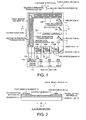
- Fig. 1 is a plan view showing a first embodiment of a touch panel device according to the invention.
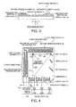
- Fig. 2 is a cross section taken along the line A-A of the touch panel device in Fig. 1.
- Fig. 3 is a cross section taken along the line B-B of the touch panel device in Fig. 1.
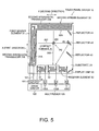
- Fig. 4 is a diagram showing a case where a contact body is touching a contact surface at a position P1.
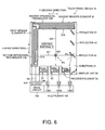
- Fig. 5 is a diagram showing a case where a contact body is touching a contact surface at a position P2.
- Fig. 6 is a diagram showing a case where a contact body is touching a contact surface at a position P3.
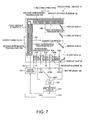
- Fig. 7 is a diagram showing a circuit section of the touch panel device according to the first embodiment of the invention.
- Figs. 8A, 8B and 8C are diagrams showing examples of loss with or without contact and an example of wave strength.
- Fig. 9 is a diagram showing a cross section taken along the line A-A of a touch panel device according to a second embodiment of the invention.
- Fig. 10 is a plan view showing a third embodiment of the invention.
- Fig. 1 is a plan view showing a first embodiment of a touch panel device 10 according to the invention.
- the touch panel device 10 can also be called an input device, a coordinate input device, or the like.
- Fig. 2 is an example of the cross-sectional configuration taken along the line A-A of the touch panel device 10 in Fig. 1.
- Fig. 3 is an example of the cross-sectional configuration taken along the line B-B of the touch panel device 10 in Fig. 1.
- the touch panel device 10 has: a display unit 20; a first sender element 31; a second sender element 32; a plurality of reflectors 41, 42 and 43; and a plurality of receiver elements 51, 52 and 53.
- the vertical direction is defined as the X-direction and the horizontal direction is defined as the Y-direction.
- the X-direction is defined as a first direction and the Y-direction is defined as a second direction.
- the touch panel device 10 can detect the coordinates or the position of a contact body, such as a finger or a stylus, on a contact surface 11 with a touch of the contact body on the contact surface 11. Therefore, the touch panel device 10 can also be used as a handwriting input device.
- a contact body such as a finger or a stylus
- the first sender element 31, the second sender element 32, the reflectors 41 to 43, and the receiver elements S to 53, which are shown in Fig. 1, are placed on a substrate 21.
- the first sender element 31 is formed on a piezoelectric material 61.
- the reflectors 41 to 43 shown in Fig. 2 are formed on another piezoelectric material 62.
- the second sender element 32 is formed on a piezoelectric material 63.
- the receiver elements 51 to 53 shown in Fig. 3 are formed on another piezoelectric material 64.
- the piezoelectric materials 61 to 64 shown in Figs. 2 and 3 are placed on the substrate 21.
- the display unit 20 has the substrate 21.
- the display unit 20 is a flat panel display device, which can be a liquid crystal display device, for example.
- the substrate 21 is a transparent glass substrate, for example.
- the piezoelectric materials 61 to 64 can be formed of piezoelectric thin film, for example, ZnO, AIN, PZT , etc.
- the piezoelectric materials 61 to 64 are not illustrated as a matter of simplification.
- the piezoelectric materials 61 to 64 are formed in a rectangular frame shape along the four sides of the substrate 21.
- the surface of the substrate 21 surrounded by the piezoelectric materials 61 to 64 is the contact surface 11 for contacting a contact body such as a finger or a stylus.
- the first embodiment shown in Figs. 1 to 3 has the contact surface 11 of an approximate square or a rectangle.
- the first sender element 31 and the second sender element 32 are interdigital transducers (IDTs) for exciting surface acoustic wave.
- IDTs interdigital transducers
- the first sender element 31 has a first interdigital transducer 31A for supplying an excitation signal and a second interdigital transducer 31B for grounding.
- the second sender element 32 has a first interdigital transducer 32A for supplying an excitation signal and a second interdigital transducer 32B for grounding.
- the first interdigital transducers 31A and 32A are electrically coupled to each other.
- the second interdigital transducers 31B and 32B are also electrically coupled to each other.
- the first interdigital transducer 31A is coupled to a drive circuit 100 so that an excitation signal 101 of the drive circuit 100 is supplied.
- the grounding interdigital transducer 31B is coupled to a grounding terminal 102 of the drive circuit 100.
- the receiver elements 51, 52 and 53 shown in Fig. 1 have the same shape.
- the receiver elements 51 to 53 have interdigital transducers 51A, 52A and 53A, respectively, for signal reception.
- the receiver elements 51 to 53 are formed on the substrate 21 along the Y-direction while facing the second sender element 32 with an interval in between.
- grounding interdigital transducers 51B, 52B and 53B are provided in the receiver elements 51, 52 and 53, respectively.
- the interdigital transducers 51A, 52A and 53A are electrically coupled to terminals 105A, 105B and 105C, respectively, of a multiplexer 105.
- the interdigital transducers 51B, 52B and 53B are coupled to a grounding terminal 106 of the drive circuit 100.
- Each of the first sender element 31, the second sender element 32, and the receiver elements 51 to 53 can be formed by means of, for example, photolithography, etc. after forming a thin film of conductive metal such as aluminum, etc. by means of evaporation, sputtering, etc.
- the reflectors 41 to 43 are placed along the X-direction at intervals. Further, the reflectors 41 to 43 are formed on the substrate 21 while facing the first sender element 31 with an interval in between.
- the reflectors 41 to 43 can be formed by means of, for example, photolithography, etc. after forming a thin film of conductive metal such as aluminum, etc. by means of evaporation, sputtering, etc.
- each of the reflectors 41 to 43 has a function for achieving the reception of the surface acoustic wave sent from the first sender element 31 on each of the receiver elements 51 to 53 by reflecting the surface acoustic wave from the first sender element 31.
- the reflector 41 is formed at an inclination angle of ⁇ 1 with respect to a line L.
- the reflector 42 is formed at an inclination angle of ⁇ 2 with respect to the line L.
- the reflector 43 is formed at an inclination angle of ⁇ 3 with respect to the line L.
- the line L is in parallel with the Y-direction, or the second direction.
- the inclination angles ⁇ 1 to ⁇ 3, which are also called reflection angles, are set within the range from ten to forty-five degrees, for example.
- the inclination angle ⁇ 1 is the largest; the inclination angle ⁇ 2 is the second largest; and the inclination angle ⁇ 3 is the smallest.
- surface acoustic wave 200 that is generated by the second sender element 32 can be received directly by the corresponding receiver elements 51 to 53.
- surface acoustic wave 201 that is generated by the first sender element 31 is first reflected on any of the corresponding reflectors 41 to 43 and then, guided by any of the corresponding receiver elements 51 to 53, received by any of the receiver elements 51 to 53.
- Figs. 4 to 6 show example cases where a contact body 400 is touching the contact surface 11.
- the contact body 400 is touching at a position corresponding to the reflector 41 and the receiver element 51.
- the contact body 400 is touching at a position corresponding to the reflector 42 and the receiver element 52.
- the contact body 400 is touching at a position corresponding to the reflector 43 and the receiver element 52.
- Fig. 7 shows an example of a circuit section provided in the touch panel device 10.
- the circuit section of the touch panel device 10 includes the drive circuit 100, the multiplexer 105, an analog-digital converter (A/D converter) 120, a detection circuit 121, and a central processing unit (CPU) 122.
- A/D converter analog-digital converter
- CPU central processing unit
- a terminal 105D of the multiplexer 105 is coupled to the detection circuit 121 via the A/D converter 120.
- the detection circuit 121 is coupled to the CPU 122.
- the drive circuit 100 supplies the excitation signal 101 to both the first interdigital transducer 31 A and the second interdigital transducer 32A, shown in Fig. 1, simultaneously in accordance with a command from the CPU 122.
- the terminal 105D of the multiplexer 105 in Fig. 7 is coupled sequentially to the terminals 105A, 105B and 105C.
- the received signal derived from the interdigital transducers 51 A, 51B and 51C is transmitted to the terminals 105A, 105B and 105C.
- the terminal 105D of the multiplexer 105 sequentially switches the terminal 105A, 105B and 105C, the signal received on the interdigital transducers 51 A, 51B and 51C is converted from analog to digital by the A/D converter 120.
- the signal converted from analog to digital is transmitted to the CPU 122 after the confirmation of signal detection by the detection circuit 121. Then, the CPU 122 judges on which one of the receiver elements 51, 52 or 53 the signal has been received.
- the contact body 400 is touching the position corresponding to the reflector 41 and the receiver element 51. That is, the contact body 400 is touching a position P1 on the contact surface 11.
- an excitation signal 201 is supplied from the drive circuit 100 simultaneously to the first interdigital transducer 31 A of the first sender element 31 and the first interdigital transducer 32A of the second sender element 32.
- the first sender element 31 and the second sender element 32 simultaneously excite the surface acoustic wave 201 and the surface acoustic wave 200, respectively.
- the surface acoustic wave 201 is excited in the Y-direction and transmitted through the contact surface 11.
- the surface acoustic wave 200 is excited in the X-direction and transmitted through the contact surface 11.
- the surface acoustic wave 201 is transmitted toward the reflector 41, being attenuated at the position P1, and reflected by the reflector 41 to be received by the receiver element 51.
- the surface acoustic wave 200 can be received directly by the receiver element 51 after being attenuated at the position P1.
- the CPU 122 shown in Fig. 7 can judge that the contact body 400 is located at the position P1.
- the other receiver elements 52 and 53 only receive the unattenuated surface acoustic wave 201 using the reflectors 42 and 43, as well as the unattenuated surface acoustic wave 200.
- the surface acoustic wave 201 is attenuated at the position P2; reflected by the reflector 42; and received by the receiver element 52.
- the surface acoustic wave 200 can be received directly by the receiver element 52 after being attenuated at the position P2.
- the CPU 122 shown in Fig. 7 can judge that the contact body 400 is located at the position P2.
- the receiver elements 51 and 53 can receive the unattenuated surface acoustic wave 201 using the reflectors 41 and 43. At the same time, the unattenuated surface acoustic wave 200 can be received directly by the receiver elements 51 and 53.
- the contact body 400 is located at the position P3 on the contact surface 11. Therefore, the attenuated surface acoustic wave 201 can be received by the receiver element 53 after being reflected by the reflector 43.
- the surface acoustic wave 200 can be received directly by the receiver element 52 after being attenuated at the position P3. Therefore, the receiver element 53 can receive the attenuated surface acoustic wave 201, and the receiver element 52 can receive the attenuated surface acoustic wave 200.
- the CPU 122 shown in Fig. 7 can judge that the contact body 400 is located at the position P3.
- Figs. 8A and 8B show examples of the extent of loss with or without the contact of the contact body on the contact surface.
- Fig. 8A shows the case where the contact body is not touching the contact surface. In this case, the loss is smaller than the one shown in Fig. 8B where the contact body is touching the contact surface.
- Fig. 8C shows the variation of wave strength with respect to time. When the contact body is touching the contact surface, the wave strength decreases at a time scale t1.
- Fig. 9 shows a second embodiment of the invention.
- a resin film 450 is provided over the contact surface 11 of the substrate 21.
- the resin film 450 is, for example, a transparent polyester film, etc.
- the resin film 450 which is provided over the contact surface 11, is kept off from the contact surface 11 with a supporting member 451 in between. Due to the above configuration, when the contact body 400 such as a finger or a stylus touches the resin film 450, the resin film 450 is depressed in the D-direction to touch the contact surface 11. Therefore, the sense of clicking can be derived using the contact body 400. Further, the resin film 450 covering the contact surface 11 prevents the contact surface 11 from being damaged. Even if the contact surface 11 is damaged with scars, etc., which affect the transmission of the surface acoustic waves 200 and 201, the fear of incorrect detection of the contact body position can be prevented.
- the touch panel device 10 has a lower electrode 650.
- the lower electrode 650 is provided between: the piezoelectric materials 61 and 62; and the substrate 21.
- Fig. 10 shows a third embodiment of the invention. What is different between the third embodiment in Fig. 10 and the first embodiment in Fig. 1 is the configuration of the reflectors 41, 42 and 43. The other components of the third embodiment in Fig. 10, which are the same as those of the first embodiment in Fig. 1, will be described using the descriptions for the corresponding components of the first embodiment.
- Each of the reflectors 41 to 43 shown in Fig. 10 has, for example, three reflecting units. That is, the reflector 41 has three reflecting units 41 A to 41C.
- the reflector 42 has other three reflecting units 42A to 42C.
- the reflector 43 has yet other three reflecting units 43A to 43C.
- each of the surface acoustic waves 201A to 201C that are excited from the first sender element 31 can be reflected on each of the reflectors 41 to 43 at a high reflectance to be received by each of the receiver elements 51 to 53 at a high signal strength.
- the receiver elements can directly receive the surface acoustic wave from the second sender element.
- the reflector reflects the surface acoustic wave from the first sender element and transmits the surface acoustic wave to be received by the receiver element.
- the electric wiring can be simplified while reducing the number of receiver elements and, with a less number of receiver elements on a substrate, the configuration of a touch panel can be simplified, leading to cost reduction due to the simplicity in mounting electric wire.
- the plurality of reflectors can reflect the surface acoustic wave from the first sender element and transmit the surface acoustic wave to be received by the receiver element.
- the invention is not limited to the above embodiments.
- the number of reflectors, the angle of the reflector, and the number of receiver elements can be varied accordingly. It is preferable that the number of reflectors and the number of receiver elements are the same. The more the numbers grow, the higher the accuracy becomes in detecting the contact position of a contact body on a contact surface.
- the display unit 20 shown in Fig. 2 is not limited to a liquid crystal display device and can be substituted by other flat panel display devices such as: field emission displays (FEDs) including surface-conduction electron-emitter displays (SEDs); and plasma displays, of course.
- FEDs field emission displays
- SEDs surface-conduction electron-emitter displays
- plasma displays of course.
- the substrate 21 can also be called a base material.
- the substrate 21 is not limited to be part of a display unit, as shown in the embodiments.
- a component other than a display unit can be provided under the substrate 21.
- Each of the configurations according to the embodiments can be partially omitted or arbitrarily combined to form different configurations.
Landscapes
- Engineering & Computer Science (AREA)
- Physics & Mathematics (AREA)
- General Engineering & Computer Science (AREA)
- Theoretical Computer Science (AREA)
- Acoustics & Sound (AREA)
- Human Computer Interaction (AREA)
- General Physics & Mathematics (AREA)
- Position Input By Displaying (AREA)
- Electronic Switches (AREA)
Abstract
Description
- The present invention relates to a touch panel device that detects the position of a contact body on the coordinate system of a contact surface by transmitting surface acoustic wave sent from a sender element and receiving the surface acoustic wave on a receiver element.
- A touch panel device has a configuration wherein the position of a contact body is detected with a touch of the contact body to a contact surface. As such a touch panel device, a configuration wherein surface acoustic wave is transmitted from an interdigital transducer on the sender side and received on another interdigital transducer on the receiver side.
- JP-UM-A-61-112444 (Fig. 4) is an example of related art.
- A coordinate detector according to the example JP-UM-A-61-112444, which is used as a touch panel device, has two sender interdigital transducers for excitation purposes and two pairs of interdigital transducers for reception purposes.
- The surface acoustic wave sent from one exciter interdigital transducer is received by one pair of receiver interdigital transducers on the opposite side. The surface acoustic wave sent from the other exciter interdigital transducer is received by the other pair of receiver interdigital transducers on the opposite side.
- Since the above configuration requires two pairs of receiver interdigital transducers and each pair further includes a plurality of interdigital transducer elements, the wiring of the electric couplings becomes very complicated. In the case of reading the coordinates of a 20 x 20 matrix, for example, forty pieces of coupling wire are required for two pairs of receiver interdigital transducers alone, which causes a problem with wiring on the substrate periphery.
- An advantage of the invention is to provide a touch panel device that requires a less number of receiver elements and therefore achieves the simplification of the configuration.
- According to a first aspect of the invention, a touch panel device includes: a substrate; a first sender element for sending surface acoustic wave, which is placed along a first direction on the substrate; a second sender element for sending surface acoustic wave, which is placed along a second direction, orthogonal to the first direction, on the substrate; a receiver element for receiving the surface acoustic wave from the second sender element, which is placed along the second direction on the substrate while facing the second sender element with an interval in between; and a reflector, which is placed on the substrate, for achieving the receiver element's reception of the surface acoustic wave from the first sender element by reflecting the surface acoustic wave from the first sender element, wherein a position of a contact body touching on a contact surface is detected by transmitting the surface acoustic wave that is sent from the sender element through the contact surface and receiving the surface acoustic wave on the receiver element.
- In the configuration according to the first aspect of the invention, the first sender element is placed along the first direction on the substrate and sends surface acoustic wave. The second sender element is placed along the second direction, orthogonal to the first direction, on the substrate and sends surface acoustic wave.
- The receiver element is placed along the second direction on the substrate while facing the second sender element with an interval in between. The receiver element receives the surface acoustic wave from the second sender element.
- The reflector, which is placed on the substrate, achieves the receiver element's reception of the surface acoustic wave from the first sender element by reflecting the surface acoustic wave from the first sender element.
- Therefore, only a single pair of receiver elements are required and the surface acoustic wave from the second sender element can be received directly by the receiver element. Further, the reflector achieves the receiver element's reception of the surface acoustic wave from the first sender element by reflecting the surface acoustic wave from the first sender element. Thus, the electric wiring can be simplified while reducing the number of receiver elements and, with the reduction in the number of receiver elements on a substrate, the configuration of a touch panel can be simplified, leading to cost reduction.
- According to a second aspect of the invention, in the touch panel device according to the first aspect of the invention, a plurality of the reflectors are placed along the first direction on the substrate while facing the first sender element with an interval in between.
- In the configuration according to the second aspect of the invention, the plurality of reflectors are placed along the first direction on the substrate while facing the first sender element with an interval in between.
- Therefore, the plurality of reflectors can achieve the receiver element's reception of the surface acoustic wave from the first sender element by reflecting the surface acoustic wave from the first sender element.
- According to a third aspect of the invention, in the touch panel device according to the first aspect of the invention, a plurality of the receiver elements are placed along the second direction.
- In the configuration according to the third aspect of the invention, the plurality of receiver elements are placed along the second direction.
- Therefore, the plurality of receiver elements can receive both the surface acoustic wave from the first sender element and the surface acoustic wave from the second sender element.
- According to a fourth aspect of the invention, in the touch panel device according to the third aspect of the invention, each of the reflectors has an individual set angle for achieving the corresponding receiver element's reception of the surface acoustic wave from the first sender element.
- In the configuration according to the fourth aspect of the invention, each of the reflectors has an individual set angle for achieving the corresponding receiver element's reception of the surface acoustic wave from the first sender element.
- Therefore, each reflector can surely achieve each receiver element's reception of the surface acoustic wave from the first sender element by reflecting the surface acoustic wave from the first sender element.
- According to a fifth aspect of the invention, in the touch panel device according to the fourth aspect of the invention, each of the reflectors has a plurality of reflecting units and the plurality of reflecting units are placed in parallel at intervals along the second direction.
- In the configuration according to the fifth aspect of the invention, each reflector has a plurality of reflecting units. The plurality of reflecting units are placed in parallel at intervals along the second direction.
- Therefore, the surface acoustic wave from the first sender element is reflected at a higher reflectance with the plurality of reflecting units included in each reflector, achieving the receiver element's reception of the surface acoustic wave from the first sender element at a higher signal strength.
- The invention will be described with reference to the accompanying drawings, wherein like numbers reference like elements.
- Fig. 1 is a plan view showing a first embodiment of a touch panel device according to the invention.
- Fig. 2 is a cross section taken along the line A-A of the touch panel device in Fig. 1.
- Fig. 3 is a cross section taken along the line B-B of the touch panel device in Fig. 1.
- Fig. 4 is a diagram showing a case where a contact body is touching a contact surface at a position P1.
- Fig. 5 is a diagram showing a case where a contact body is touching a contact surface at a position P2.
- Fig. 6 is a diagram showing a case where a contact body is touching a contact surface at a position P3.
- Fig. 7 is a diagram showing a circuit section of the touch panel device according to the first embodiment of the invention.
- Figs. 8A, 8B and 8C are diagrams showing examples of loss with or without contact and an example of wave strength.
- Fig. 9 is a diagram showing a cross section taken along the line A-A of a touch panel device according to a second embodiment of the invention.
- Fig. 10 is a plan view showing a third embodiment of the invention.
- Embodiments of the invention will now be described with reference to the accompanying drawings.
- Fig. 1 is a plan view showing a first embodiment of a
touch panel device 10 according to the invention. Thetouch panel device 10 can also be called an input device, a coordinate input device, or the like. - Fig. 2 is an example of the cross-sectional configuration taken along the line A-A of the
touch panel device 10 in Fig. 1. Fig. 3 is an example of the cross-sectional configuration taken along the line B-B of thetouch panel device 10 in Fig. 1. - As shown in Figs. 1 to 3, the
touch panel device 10 has: adisplay unit 20; afirst sender element 31; asecond sender element 32; a plurality ofreflectors receiver elements - In Fig. 1, the vertical direction is defined as the X-direction and the horizontal direction is defined as the Y-direction. The X-direction is defined as a first direction and the Y-direction is defined as a second direction.
- The
touch panel device 10 can detect the coordinates or the position of a contact body, such as a finger or a stylus, on acontact surface 11 with a touch of the contact body on thecontact surface 11. Therefore, thetouch panel device 10 can also be used as a handwriting input device. - The
first sender element 31, thesecond sender element 32, thereflectors 41 to 43, and the receiver elements S to 53, which are shown in Fig. 1, are placed on asubstrate 21. - As shown in Fig. 2, the
first sender element 31 is formed on apiezoelectric material 61. Thereflectors 41 to 43 shown in Fig. 2 are formed on anotherpiezoelectric material 62. - As shown in Fig. 3, the
second sender element 32 is formed on apiezoelectric material 63. Thereceiver elements 51 to 53 shown in Fig. 3 are formed on anotherpiezoelectric material 64. - The
piezoelectric materials 61 to 64 shown in Figs. 2 and 3 are placed on thesubstrate 21. - The
display unit 20 has thesubstrate 21. Thedisplay unit 20 is a flat panel display device, which can be a liquid crystal display device, for example. Thesubstrate 21 is a transparent glass substrate, for example. Thepiezoelectric materials 61 to 64 can be formed of piezoelectric thin film, for example, ZnO, AIN, PZT , etc. - In Fig. 1, the
piezoelectric materials 61 to 64 are not illustrated as a matter of simplification. - As shown in Figs. 2 and 3, the
piezoelectric materials 61 to 64 are formed in a rectangular frame shape along the four sides of thesubstrate 21. The surface of thesubstrate 21 surrounded by thepiezoelectric materials 61 to 64 is thecontact surface 11 for contacting a contact body such as a finger or a stylus. The first embodiment shown in Figs. 1 to 3 has thecontact surface 11 of an approximate square or a rectangle. - The
first sender element 31 and thesecond sender element 32 are interdigital transducers (IDTs) for exciting surface acoustic wave. - As shown in Fig. 1, the
first sender element 31 has a firstinterdigital transducer 31A for supplying an excitation signal and a secondinterdigital transducer 31B for grounding. Likewise, thesecond sender element 32 has a firstinterdigital transducer 32A for supplying an excitation signal and a secondinterdigital transducer 32B for grounding. The firstinterdigital transducers interdigital transducers - The first
interdigital transducer 31A is coupled to adrive circuit 100 so that anexcitation signal 101 of thedrive circuit 100 is supplied. The groundinginterdigital transducer 31B is coupled to agrounding terminal 102 of thedrive circuit 100. - The
receiver elements receiver elements 51 to 53 haveinterdigital transducers receiver elements 51 to 53 are formed on thesubstrate 21 along the Y-direction while facing thesecond sender element 32 with an interval in between. Corresponding to theinterdigital transducers interdigital transducers receiver elements - The
interdigital transducers terminals multiplexer 105. Theinterdigital transducers grounding terminal 106 of thedrive circuit 100. - Each of the
first sender element 31, thesecond sender element 32, and thereceiver elements 51 to 53 can be formed by means of, for example, photolithography, etc. after forming a thin film of conductive metal such as aluminum, etc. by means of evaporation, sputtering, etc. - Next, the
reflectors 41 to 43 shown in Fig. 1 will be described. - The
reflectors 41 to 43 are placed along the X-direction at intervals. Further, thereflectors 41 to 43 are formed on thesubstrate 21 while facing thefirst sender element 31 with an interval in between. Thereflectors 41 to 43 can be formed by means of, for example, photolithography, etc. after forming a thin film of conductive metal such as aluminum, etc. by means of evaporation, sputtering, etc. - What is characteristic is that each of the
reflectors 41 to 43 has a function for achieving the reception of the surface acoustic wave sent from thefirst sender element 31 on each of thereceiver elements 51 to 53 by reflecting the surface acoustic wave from thefirst sender element 31. - The
reflector 41 is formed at an inclination angle of θ1 with respect to a line L. Likewise, thereflector 42 is formed at an inclination angle of θ2 with respect to the line L. Thereflector 43 is formed at an inclination angle of θ3 with respect to the line L. The line L is in parallel with the Y-direction, or the second direction. - It is preferable that the inclination angles θ1 to θ3, which are also called reflection angles, are set within the range from ten to forty-five degrees, for example. In the example shown in Fig. 1, wherein the total of three
reflectors 41 to 43 are provided, the inclination angle θ1 is the largest; the inclination angle θ2 is the second largest; and the inclination angle θ3 is the smallest. - In Fig. 1, surface
acoustic wave 200 that is generated by thesecond sender element 32 can be received directly by the correspondingreceiver elements 51 to 53. - On the other hand, surface
acoustic wave 201 that is generated by thefirst sender element 31 is first reflected on any of the correspondingreflectors 41 to 43 and then, guided by any of the correspondingreceiver elements 51 to 53, received by any of thereceiver elements 51 to 53. - Figs. 4 to 6 show example cases where a
contact body 400 is touching thecontact surface 11. In the example shown in Fig. 4, thecontact body 400 is touching at a position corresponding to thereflector 41 and thereceiver element 51. In the example shown in Fig. 5, thecontact body 400 is touching at a position corresponding to thereflector 42 and thereceiver element 52. In the example shown in Fig. 6, thecontact body 400 is touching at a position corresponding to thereflector 43 and thereceiver element 52. - Fig. 7 shows an example of a circuit section provided in the
touch panel device 10. The circuit section of thetouch panel device 10 includes thedrive circuit 100, themultiplexer 105, an analog-digital converter (A/D converter) 120, adetection circuit 121, and a central processing unit (CPU) 122. - A terminal 105D of the
multiplexer 105 is coupled to thedetection circuit 121 via the A/D converter 120. Thedetection circuit 121 is coupled to theCPU 122. Thedrive circuit 100 supplies theexcitation signal 101 to both the firstinterdigital transducer 31 A and the secondinterdigital transducer 32A, shown in Fig. 1, simultaneously in accordance with a command from theCPU 122. - The terminal 105D of the
multiplexer 105 in Fig. 7 is coupled sequentially to theterminals interdigital transducers terminals multiplexer 105 sequentially switches the terminal 105A, 105B and 105C, the signal received on theinterdigital transducers D converter 120. The signal converted from analog to digital is transmitted to theCPU 122 after the confirmation of signal detection by thedetection circuit 121. Then, theCPU 122 judges on which one of thereceiver elements - Next, examples of how the
CPU 122 detects the position of thecontact body 400 on thecontact surface 11, as shown in Figs. 4 to 6, will be described. - In the example shown in Fig. 4, the
contact body 400 is touching the position corresponding to thereflector 41 and thereceiver element 51. That is, thecontact body 400 is touching a position P1 on thecontact surface 11. - In any example shown in Figs. 4 to 6, an
excitation signal 201 is supplied from thedrive circuit 100 simultaneously to the firstinterdigital transducer 31 A of thefirst sender element 31 and the firstinterdigital transducer 32A of thesecond sender element 32. - Therefore, the
first sender element 31 and thesecond sender element 32 simultaneously excite the surfaceacoustic wave 201 and the surfaceacoustic wave 200, respectively. The surfaceacoustic wave 201 is excited in the Y-direction and transmitted through thecontact surface 11. The surfaceacoustic wave 200 is excited in the X-direction and transmitted through thecontact surface 11. - In the example shown in Fig. 4, wherein the
contact body 400 is located at the position P1, the surfaceacoustic wave 201 is transmitted toward thereflector 41, being attenuated at the position P1, and reflected by thereflector 41 to be received by thereceiver element 51. At the same time, the surfaceacoustic wave 200 can be received directly by thereceiver element 51 after being attenuated at the position P1. - Since the
receiver element 51 can receive both the surfaceacoustic wave 201 and the surfaceacoustic wave 200 that are attenuated by thecontact body 400, theCPU 122 shown in Fig. 7 can judge that thecontact body 400 is located at the position P1. - The
other receiver elements acoustic wave 201 using thereflectors acoustic wave 200. - In the example shown in Fig. 5, wherein the
contact body 400 is located at the position P2 on thecontact surface 11, the surfaceacoustic wave 201 is attenuated at the position P2; reflected by thereflector 42; and received by thereceiver element 52. The surfaceacoustic wave 200 can be received directly by thereceiver element 52 after being attenuated at the position P2. - In the above method, since the
receiver element 52 can receive the attenuated surfaceacoustic wave 201 and the attenuated surfaceacoustic wave 200, theCPU 122 shown in Fig. 7 can judge that thecontact body 400 is located at the position P2. - In the above case, the
receiver elements acoustic wave 201 using thereflectors acoustic wave 200 can be received directly by thereceiver elements - In the example shown in Fig. 6, the
contact body 400 is located at the position P3 on thecontact surface 11. Therefore, the attenuated surfaceacoustic wave 201 can be received by thereceiver element 53 after being reflected by thereflector 43. The surfaceacoustic wave 200 can be received directly by thereceiver element 52 after being attenuated at the position P3. Therefore, thereceiver element 53 can receive the attenuated surfaceacoustic wave 201, and thereceiver element 52 can receive the attenuated surfaceacoustic wave 200. - In the above method, the
CPU 122 shown in Fig. 7 can judge that thecontact body 400 is located at the position P3. - Figs. 8A and 8B show examples of the extent of loss with or without the contact of the contact body on the contact surface.
- Fig. 8A shows the case where the contact body is not touching the contact surface. In this case, the loss is smaller than the one shown in Fig. 8B where the contact body is touching the contact surface. Fig. 8C shows the variation of wave strength with respect to time. When the contact body is touching the contact surface, the wave strength decreases at a time scale t1.
- Fig. 9 shows a second embodiment of the invention.
- In the second embodiment shown in Fig. 9, in addition to the same configuration as the embodiment shown in Figs. 1 to 3, a
resin film 450 is provided over thecontact surface 11 of thesubstrate 21. Theresin film 450 is, for example, a transparent polyester film, etc. Theresin film 450, which is provided over thecontact surface 11, is kept off from thecontact surface 11 with a supportingmember 451 in between. Due to the above configuration, when thecontact body 400 such as a finger or a stylus touches theresin film 450, theresin film 450 is depressed in the D-direction to touch thecontact surface 11. Therefore, the sense of clicking can be derived using thecontact body 400. Further, theresin film 450 covering thecontact surface 11 prevents thecontact surface 11 from being damaged. Even if thecontact surface 11 is damaged with scars, etc., which affect the transmission of the surfaceacoustic waves - The
touch panel device 10 has alower electrode 650. Thelower electrode 650 is provided between: thepiezoelectric materials substrate 21. - Fig. 10 shows a third embodiment of the invention. What is different between the third embodiment in Fig. 10 and the first embodiment in Fig. 1 is the configuration of the
reflectors - Each of the
reflectors 41 to 43 shown in Fig. 10 has, for example, three reflecting units. That is, thereflector 41 has three reflectingunits 41 A to 41C. Thereflector 42 has other three reflectingunits 42A to 42C. Thereflector 43 has yet other three reflectingunits 43A to 43C. - As described above, by providing a plurality of reflecting units in each of the
reflectors 41 to 43, an advantage arises that each of the surfaceacoustic waves 201A to 201C that are excited from thefirst sender element 31 can be reflected on each of thereflectors 41 to 43 at a high reflectance to be received by each of thereceiver elements 51 to 53 at a high signal strength. - In the embodiments of the invention, only a single pair of receiver elements is required. Further, the receiver elements can directly receive the surface acoustic wave from the second sender element. In addition, the reflector reflects the surface acoustic wave from the first sender element and transmits the surface acoustic wave to be received by the receiver element. Thus, the electric wiring can be simplified while reducing the number of receiver elements and, with a less number of receiver elements on a substrate, the configuration of a touch panel can be simplified, leading to cost reduction due to the simplicity in mounting electric wire. The plurality of reflectors can reflect the surface acoustic wave from the first sender element and transmit the surface acoustic wave to be received by the receiver element.
- The invention is not limited to the above embodiments. For example, the number of reflectors, the angle of the reflector, and the number of receiver elements can be varied accordingly. It is preferable that the number of reflectors and the number of receiver elements are the same. The more the numbers grow, the higher the accuracy becomes in detecting the contact position of a contact body on a contact surface.
- For example, the
display unit 20 shown in Fig. 2 is not limited to a liquid crystal display device and can be substituted by other flat panel display devices such as: field emission displays (FEDs) including surface-conduction electron-emitter displays (SEDs); and plasma displays, of course. - In the embodiments of the invention, the
substrate 21 can also be called a base material. Thesubstrate 21 is not limited to be part of a display unit, as shown in the embodiments. A component other than a display unit can be provided under thesubstrate 21. - The invention is not limited to the above embodiments and can be modified variously without departing from what is claimed.
- Each of the configurations according to the embodiments can be partially omitted or arbitrarily combined to form different configurations.
Claims (5)
- A touch panel device, comprising:a substrate;a first sender element for sending surface acoustic wave, which is placed along a first direction on the substrate;a second sender element for sending surface acoustic wave, which is placed along a second direction, orthogonal to the first direction, on the substrate;a receiver element for receiving the surface acoustic wave from the second sender element, which is placed along the second direction on the substrate while facing the second sender element with an interval in between; anda reflector, which is placed on the substrate, for achieving the receiver element's reception of the surface acoustic wave from the first sender element by reflecting the surface acoustic wave from the first sender element,wherein a position of a contact body touching on a contact surface is detected by transmitting the surface acoustic wave that is sent from the sender element through the contact surface and receiving the surface acoustic wave on the receiver element.
- The touch panel device according to Claim 1, wherein a plurality of the reflectors are placed along the first direction on the substrate while facing the first sender element with an interval in between.
- The touch panel device according to Claim 1, wherein a plurality of the receiver elements are placed along the second direction.
- The touch panel device according to Claim 3, wherein each of the reflectors has an individual set angle for achieving the corresponding receiver element's reception of the surface acoustic wave from the first sender element.
- The touch panel device according to Claim 4, wherein each of the reflectors has a plurality of reflecting units and the plurality of reflecting units are placed in parallel at intervals along the second direction.
Applications Claiming Priority (1)
| Application Number | Priority Date | Filing Date | Title |
|---|---|---|---|
| JP2004380850A JP4151075B2 (en) | 2004-12-28 | 2004-12-28 | Touch panel device |
Publications (2)
| Publication Number | Publication Date |
|---|---|
| EP1677181A2 true EP1677181A2 (en) | 2006-07-05 |
| EP1677181A3 EP1677181A3 (en) | 2007-07-11 |
Family
ID=36088356
Family Applications (1)
| Application Number | Title | Priority Date | Filing Date |
|---|---|---|---|
| EP05028536A Withdrawn EP1677181A3 (en) | 2004-12-28 | 2005-12-27 | Touch panel device |
Country Status (6)
| Country | Link |
|---|---|
| US (1) | US7659889B2 (en) |
| EP (1) | EP1677181A3 (en) |
| JP (1) | JP4151075B2 (en) |
| KR (1) | KR100738751B1 (en) |
| CN (1) | CN100367177C (en) |
| TW (1) | TWI303774B (en) |
Cited By (1)
| Publication number | Priority date | Publication date | Assignee | Title |
|---|---|---|---|---|
| JP2019525448A (en) * | 2016-05-24 | 2019-09-05 | ルクセンブルク インスティトゥート オブ サイエンス アンド テクノロジー(リスト) | Transparent piezoelectric device and method for manufacturing the same |
Families Citing this family (7)
| Publication number | Priority date | Publication date | Assignee | Title |
|---|---|---|---|---|
| TWI315842B (en) * | 2006-07-10 | 2009-10-11 | Egalax Empia Technology Inc | Surface acoustic wave touch panel with interdigital transducers |
| TWI383313B (en) * | 2007-06-13 | 2013-01-21 | 禾瑞亞科技股份有限公司 | Surface acoustic wave touch panel sensing device |
| CN101685212B (en) | 2008-09-26 | 2012-08-29 | 群康科技(深圳)有限公司 | Liquid crystal display panel |
| TW201113787A (en) * | 2009-10-05 | 2011-04-16 | Au Optronics Corp | Touch display panel and display device |
| US8576202B2 (en) * | 2010-03-25 | 2013-11-05 | Elo Touch Solutions, Inc. | Bezel-less acoustic touch apparatus |
| KR101491933B1 (en) * | 2013-11-19 | 2015-02-09 | 엘에스산전 주식회사 | Apparatus for controlling paralleled inverter |
| US10877097B2 (en) | 2019-02-06 | 2020-12-29 | Power Standard Labs, Inc. | DC monitoring system for variable frequency drives |
Family Cites Families (14)
| Publication number | Priority date | Publication date | Assignee | Title |
|---|---|---|---|---|
| JPS61112444A (en) | 1984-10-09 | 1986-05-30 | Power Reactor & Nuclear Fuel Dev Corp | Structure of transmission path for wall body passing information |
| US4700176A (en) * | 1985-02-05 | 1987-10-13 | Zenith Electronis Corporation | Tough control arrangement for graphics display apparatus |
| JPH06149458A (en) | 1992-10-12 | 1994-05-27 | Koji Toda | Ultrasonic information device |
| US5591945A (en) * | 1995-04-19 | 1997-01-07 | Elo Touchsystems, Inc. | Acoustic touch position sensor using higher order horizontally polarized shear wave propagation |
| KR100207420B1 (en) | 1995-12-29 | 1999-07-15 | 전주범 | Touch screen |
| JPH11327772A (en) * | 1998-05-07 | 1999-11-30 | Ricoh Co Ltd | Ultrasonic touch panel |
| JP4024933B2 (en) | 1998-08-18 | 2007-12-19 | タッチパネル・システムズ株式会社 | Touch panel |
| WO2001057636A1 (en) | 2000-01-31 | 2001-08-09 | Touch Panel Systems K.K. | Touch panel |
| JP2002041232A (en) | 2000-07-21 | 2002-02-08 | Daicel Chem Ind Ltd | Acoustic contact detection device |
| JP2002236541A (en) * | 2001-02-09 | 2002-08-23 | Ricoh Co Ltd | Position detecting device, touch panel using the same, portable device, and shape detecting device |
| US6836367B2 (en) | 2001-02-28 | 2004-12-28 | Japan Aviation Electronics Industry, Limited | Optical touch panel |
| CN2519331Y (en) * | 2002-01-30 | 2002-10-30 | 成都吉锐触摸电脑有限公司 | Surface sound wave touch screen for increase effective touch district through touch district step enlargement |
| JP2003091357A (en) * | 2001-09-18 | 2003-03-28 | Ricoh Co Ltd | Coordinate input device |
| KR100533642B1 (en) * | 2004-03-29 | 2005-12-06 | 삼성전기주식회사 | An apparatus for detecting the touch position using surface acoustic wave |
-
2004
- 2004-12-28 JP JP2004380850A patent/JP4151075B2/en not_active Expired - Fee Related
-
2005
- 2005-12-14 US US11/300,105 patent/US7659889B2/en not_active Expired - Fee Related
- 2005-12-15 TW TW094144475A patent/TWI303774B/en not_active IP Right Cessation
- 2005-12-27 KR KR1020050130453A patent/KR100738751B1/en not_active Expired - Fee Related
- 2005-12-27 EP EP05028536A patent/EP1677181A3/en not_active Withdrawn
- 2005-12-27 CN CNB2005101340891A patent/CN100367177C/en not_active Expired - Fee Related
Cited By (1)
| Publication number | Priority date | Publication date | Assignee | Title |
|---|---|---|---|---|
| JP2019525448A (en) * | 2016-05-24 | 2019-09-05 | ルクセンブルク インスティトゥート オブ サイエンス アンド テクノロジー(リスト) | Transparent piezoelectric device and method for manufacturing the same |
Also Published As
| Publication number | Publication date |
|---|---|
| JP4151075B2 (en) | 2008-09-17 |
| KR100738751B1 (en) | 2007-07-12 |
| JP2006185362A (en) | 2006-07-13 |
| KR20060076712A (en) | 2006-07-04 |
| US20060139341A1 (en) | 2006-06-29 |
| CN100367177C (en) | 2008-02-06 |
| TWI303774B (en) | 2008-12-01 |
| EP1677181A3 (en) | 2007-07-11 |
| US7659889B2 (en) | 2010-02-09 |
| CN1797307A (en) | 2006-07-05 |
| TW200707262A (en) | 2007-02-16 |
Similar Documents
| Publication | Publication Date | Title |
|---|---|---|
| US8941624B2 (en) | Acoustic touch sensor utilizing edge waves | |
| EP2385444B1 (en) | Acoustic touch sensor | |
| TW494349B (en) | Acoustic touch sensor | |
| KR100744866B1 (en) | Touch panel device | |
| US6911973B2 (en) | Touch panel device | |
| JP2003345504A (en) | Touch panel device | |
| JP2001014093A (en) | Acoustic contact detection device | |
| CN101167044A (en) | Information input device | |
| KR20220002111A (en) | Ultrasonic water-agnostic touch detection sensor | |
| US7659889B2 (en) | Touch panel device | |
| EP1796129A1 (en) | Contact detectiing function-carrying display unit | |
| JPH10240428A (en) | Ultrasonic touch panel | |
| JPH1131049A (en) | Coordinate input device | |
| JPH08305481A (en) | Touch input device | |
| JP2007065800A (en) | Touch panel device | |
| JP2006285420A (en) | Touch panel and touch panel type coordinate input method | |
| JPH08305482A (en) | Touch input device | |
| JPH1055246A (en) | Ultrasonic touch panel | |
| JPH1055244A (en) | Ultrasonic touch panel | |
| JP3959534B2 (en) | Ultrasonic touch panel | |
| JPH1055239A (en) | Ultrasonic touch panel | |
| WO2001002943A1 (en) | Acoustic touch sensor | |
| JP2007065799A (en) | Touch panel device | |
| JPH1055241A (en) | Ultrasonic touch panel | |
| JPH10207614A (en) | Coordinate position input device |
Legal Events
| Date | Code | Title | Description |
|---|---|---|---|
| PUAI | Public reference made under article 153(3) epc to a published international application that has entered the european phase |
Free format text: ORIGINAL CODE: 0009012 |
|
| AK | Designated contracting states |
Kind code of ref document: A2 Designated state(s): AT BE BG CH CY CZ DE DK EE ES FI FR GB GR HU IE IS IT LI LT LU LV MC NL PL PT RO SE SI SK TR |
|
| AX | Request for extension of the european patent |
Extension state: AL BA HR MK YU |
|
| PUAL | Search report despatched |
Free format text: ORIGINAL CODE: 0009013 |
|
| AK | Designated contracting states |
Kind code of ref document: A3 Designated state(s): AT BE BG CH CY CZ DE DK EE ES FI FR GB GR HU IE IS IT LI LT LU LV MC NL PL PT RO SE SI SK TR |
|
| AX | Request for extension of the european patent |
Extension state: AL BA HR MK YU |
|
| 17P | Request for examination filed |
Effective date: 20071011 |
|
| 17Q | First examination report despatched |
Effective date: 20071109 |
|
| AKX | Designation fees paid |
Designated state(s): DE FR GB |
|
| STAA | Information on the status of an ep patent application or granted ep patent |
Free format text: STATUS: THE APPLICATION IS DEEMED TO BE WITHDRAWN |
|
| 18D | Application deemed to be withdrawn |
Effective date: 20100701 |