EP1677130A1 - Method of dividing a guide electromagnetic signal into two half-power signals, using photonic crystals - Google Patents
Method of dividing a guide electromagnetic signal into two half-power signals, using photonic crystals Download PDFInfo
- Publication number
- EP1677130A1 EP1677130A1 EP04766917A EP04766917A EP1677130A1 EP 1677130 A1 EP1677130 A1 EP 1677130A1 EP 04766917 A EP04766917 A EP 04766917A EP 04766917 A EP04766917 A EP 04766917A EP 1677130 A1 EP1677130 A1 EP 1677130A1
- Authority
- EP
- European Patent Office
- Prior art keywords
- coupler
- photonic crystals
- dividing
- guides
- electromagnetic signal
- Prior art date
- Legal status (The legal status is an assumption and is not a legal conclusion. Google has not performed a legal analysis and makes no representation as to the accuracy of the status listed.)
- Withdrawn
Links
- 239000004038 photonic crystal Substances 0.000 title claims abstract description 48
- 238000000034 method Methods 0.000 title claims abstract description 30
- 239000013078 crystal Substances 0.000 claims description 13
- 238000000926 separation method Methods 0.000 abstract description 8
- 230000005540 biological transmission Effects 0.000 abstract description 7
- 230000003595 spectral effect Effects 0.000 description 16
- 230000003287 optical effect Effects 0.000 description 11
- 230000004044 response Effects 0.000 description 10
- 230000008878 coupling Effects 0.000 description 8
- 238000010168 coupling process Methods 0.000 description 8
- 238000005859 coupling reaction Methods 0.000 description 8
- 230000007547 defect Effects 0.000 description 7
- 239000000463 material Substances 0.000 description 7
- 230000010287 polarization Effects 0.000 description 7
- 230000008901 benefit Effects 0.000 description 6
- 230000000737 periodic effect Effects 0.000 description 6
- 238000005516 engineering process Methods 0.000 description 5
- 238000005259 measurement Methods 0.000 description 4
- 238000004088 simulation Methods 0.000 description 4
- 238000012546 transfer Methods 0.000 description 4
- 230000006978 adaptation Effects 0.000 description 3
- 230000005684 electric field Effects 0.000 description 3
- 230000005284 excitation Effects 0.000 description 3
- 238000004519 manufacturing process Methods 0.000 description 3
- PNEYBMLMFCGWSK-UHFFFAOYSA-N aluminium oxide Inorganic materials [O-2].[O-2].[O-2].[Al+3].[Al+3] PNEYBMLMFCGWSK-UHFFFAOYSA-N 0.000 description 2
- 239000006185 dispersion Substances 0.000 description 2
- 230000010354 integration Effects 0.000 description 2
- 230000009191 jumping Effects 0.000 description 2
- 238000012545 processing Methods 0.000 description 2
- 238000000411 transmission spectrum Methods 0.000 description 2
- 241001482107 Alosa sapidissima Species 0.000 description 1
- XUIMIQQOPSSXEZ-UHFFFAOYSA-N Silicon Chemical compound [Si] XUIMIQQOPSSXEZ-UHFFFAOYSA-N 0.000 description 1
- 238000013459 approach Methods 0.000 description 1
- 238000004891 communication Methods 0.000 description 1
- 230000000295 complement effect Effects 0.000 description 1
- 230000007423 decrease Effects 0.000 description 1
- 230000001934 delay Effects 0.000 description 1
- 238000013461 design Methods 0.000 description 1
- 238000011161 development Methods 0.000 description 1
- 239000003989 dielectric material Substances 0.000 description 1
- 230000000694 effects Effects 0.000 description 1
- 239000000835 fiber Substances 0.000 description 1
- 238000003780 insertion Methods 0.000 description 1
- 230000037431 insertion Effects 0.000 description 1
- 230000007246 mechanism Effects 0.000 description 1
- 239000013307 optical fiber Substances 0.000 description 1
- 230000008569 process Effects 0.000 description 1
- 230000000644 propagated effect Effects 0.000 description 1
- 230000009467 reduction Effects 0.000 description 1
- 229910052710 silicon Inorganic materials 0.000 description 1
- 239000010703 silicon Substances 0.000 description 1
- 239000000758 substrate Substances 0.000 description 1
- 230000001629 suppression Effects 0.000 description 1
- 230000001360 synchronised effect Effects 0.000 description 1
- 230000036964 tight binding Effects 0.000 description 1
- 238000012795 verification Methods 0.000 description 1
- 238000012800 visualization Methods 0.000 description 1
Images





Classifications
-
- B—PERFORMING OPERATIONS; TRANSPORTING
- B82—NANOTECHNOLOGY
- B82Y—SPECIFIC USES OR APPLICATIONS OF NANOSTRUCTURES; MEASUREMENT OR ANALYSIS OF NANOSTRUCTURES; MANUFACTURE OR TREATMENT OF NANOSTRUCTURES
- B82Y20/00—Nanooptics, e.g. quantum optics or photonic crystals
-
- G—PHYSICS
- G02—OPTICS
- G02B—OPTICAL ELEMENTS, SYSTEMS OR APPARATUS
- G02B6/00—Light guides; Structural details of arrangements comprising light guides and other optical elements, e.g. couplings
- G02B6/10—Light guides; Structural details of arrangements comprising light guides and other optical elements, e.g. couplings of the optical waveguide type
- G02B6/12—Light guides; Structural details of arrangements comprising light guides and other optical elements, e.g. couplings of the optical waveguide type of the integrated circuit kind
- G02B6/122—Basic optical elements, e.g. light-guiding paths
- G02B6/125—Bends, branchings or intersections
-
- G—PHYSICS
- G02—OPTICS
- G02B—OPTICAL ELEMENTS, SYSTEMS OR APPARATUS
- G02B6/00—Light guides; Structural details of arrangements comprising light guides and other optical elements, e.g. couplings
- G02B6/10—Light guides; Structural details of arrangements comprising light guides and other optical elements, e.g. couplings of the optical waveguide type
- G02B6/12—Light guides; Structural details of arrangements comprising light guides and other optical elements, e.g. couplings of the optical waveguide type of the integrated circuit kind
- G02B6/122—Basic optical elements, e.g. light-guiding paths
- G02B6/1225—Basic optical elements, e.g. light-guiding paths comprising photonic band-gap structures or photonic lattices
Definitions
- the present invention consists of a method that allows the power of an input electromagnetic signal to be divided into two equal-power signals with a relative phase difference of 180° and an equal propagation delay.
- This method makes use of a coupler consisting of two parallel guides disposed close to one another in a photonic crystal. Both two-dimensional (2D) and three-dimensional (3D) crystals could be used as the underlying concept is the same.
- the advantages of the divider structure are its small size, which makes it suitable for integration of numerous dividing units as functional units of more complex devices, the high operational bandwidth, which is an advantage with respect to other methods for dividing power which are sensitive to frequency, and synchrony between the output signals from the device, which is an essential feature for high-speed signal processing.
- the field for application of the present invention is in any device based on 2D or 3D photonic crystal technology designed to operate over any frequency range, from optical signals and microwave/millimeter signals, to signals with frequencies in the visible or infrared range.
- Photonic crystals are formed from materials with a dielectric constant that varies periodically in one, two or three spatial dimensions. This periodicity gives rise to the appearance of frequency bands in which signal propagation is not permitted inside the crystal. These forbidden frequency bands are commonly known as the Photonic Band Gap (PBG).
- PBG Photonic Band Gap
- Light propagation can be controlled by inserting defects that alter the periodicity of the crystal. The insertion of linear defects leads to the appearance of guided modes at frequencies within the forbidden band allowing the propagation of light only in the defect created.
- total control of the propagation of light is achieved by using 3D photonic crystals, control of light in three dimensions can also be achieved with planar 2D photonic crystals, thus reducing the cost and complexity of manufacture.
- the light is confined to the direction perpendicular to the plane of the crystal if the dielectric constant of the materials above and below the crystal is less than the dielectric constant of the defect created in the crystal.
- photonic crystals Due to the scaling properties of Maxwell's equations, photonic crystals can be made to have a forbidden band in any spectral range provided the structure is appropriately scaled and provided materials are chosen that have suitable properties in the chosen spectral range.
- photonic crystals have been implemented to work at microwave frequencies where the periodicity is of the order of cm. To do this, bars of dielectric material with a high refraction index are used that form periodic lattices in air. The properties of these structures can by and large be extrapolated to the structures corresponding to optical frequencies, but with the advantage that at microwave frequencies, manufacture and measurement of the properties is much easier.
- a waveguide can be created from a chain of equally spaced cavities or point defects along a certain direction of the crystal.
- This type of guide is known as a coupled cavity waveguide.
- the propagation along these guides is explained by photons jumping between adjacent cavities due to overlap of the evanescent field tails.
- the coupled cavity waveguides have certain characteristics that make them particularly interesting: on the one hand, a theoretical expression can be derived for the dispersion ratio of the guide modes from tight-binding approach used in solid-state physics. On the other hand, transmission along curves with very tightly curved radii is very efficient provided that symmetry of the cavity mode is appropriate.
- the group velocity of this type of guide is very low, tending to zero at the edges of the band, and so highly efficient non-linear processes are expected in this type of guide, as well as high dispersion that could be of use in a number of applications.
- couplers in photonic crystal technology can be implemented in the same way as used by other more mature technologies, such as integrated guides or fiber optics: disposing two parallel wave guides close to one another. If both guides are identical and single moded when placed in proximity, the two interact and the guide mode of an isolated guide divides into two modes for the complete system of the two parallel waveguides. These modes have even and odd symmetry with respect to the plane equidistant from the guide axis. In addition, these modes have different propagation constants, implying that they travel at a different velocity along the coupler. This behavior causes a signal to be excited in one of the two guides, after a certain distance the wave passes to the adjacent guide and, once again, returns to the original guide after covering the same distance.
- the power dividers/combiners are fundamental blocks in any optical network or device. Their function is to distribute the power of an input signal to two output ports with certain percentages at each output. If the percentages are 50%, the divider is usually called a 3 dB divider.
- These blocks can be implemented mainly in two ways (see Figures 1a and 1b): either using a directional coupler designed such that the power is divided equally between the output ports at on output ( Figure 1a), or by means of a Y-shaped structure in which the input guide divides into two output guides at a certain angle to minimize losses (Figure 1b).
- Figure 1a directional coupler designed such that the power is divided equally between the output ports at on output
- Figure 1b a Y-shaped structure in which the input guide divides into two output guides at a certain angle to minimize losses
- the phase difference between the output signals is 90% whereas for the second case, both outputs are in phase.
- the implementation of Y-shaped dividers has also been proposed in photonic crystal technology and it has
- the invention relates to a method of dividing the power of an input electromagnetic signal into two equal-power signals with a relative phase difference between the two of 180° and an equal propagation delay.
- the structure can also be designed so that the phase difference between output signals is 0° although, whatever the phase difference, the output signals travel the same physical path and are in synchrony.
- Said method makes use of a coupler implemented in a photonic crystal and consisting of two parallel guides located close to one another and based on coupled cavities.
- the physical basis of the proposed method is based on exciting the odd mode of the coupler, which because of its symmetry, ensures that field maxima in one guide coincide with minima in the adjacent guide so achieving a relative phase difference of 180 degrees.
- the two output signals are obtained by spatial separation of the guides that make up the coupler, making use of the property that possess the guides in photonic crystals of high transmission efficiency through tight curves, a property which allows the size of the structure to be considerably reduced.
- the method is valid both for two-dimensional (2D) and three-dimensional (3D) photonic crystals as the underlying concept is the same.
- the advantages of the divider structure are its small size, which makes it suitable for integration of several dividing units as functional units of more complex devices, large bandwidth, and synchronization of the two output signals of the structure, which allows high-speed signal processing.
- a divider could be obtained with the output signals in-phase if, instead of odd mode, the even mode of the coupler is used.
- the photonic crystal comprises a lattice of cylinders grouped in columns that can adopt any value for the lattice constant (distance between cylinders closest to one another), was well as any radius and height of the cylinders. Likewise, the method is applicable for any difference of refraction indexes between the material of the columns, the material that surrounds the columns and the material above and below the crystal.
- the photonic crystals can adopt any type of lattice, particularly a triangular lattice or square lattice.
- the dielectric guide can have any type of configuration to create the coupler, (width and height of the nucleus and layers that surround it), was well as any refraction index, including also the optical fiber.
- the method is likewise applicable to any type of guide in a photonic crystal that is used to inject and extract signals from the coupling region.
- Figure 1 shows the two structures that are widely used in optical circuits to divide the power of an input signal at two output ports:
- Figure 1a shows the directional coupler formed from two equal parallel guides close to one another in which periodic transfer of power between guides occurs in the coupling region (4) such that with suitable selection of the length of the coupler, it is possible to obtain a certain ratio of powers at the output ports (2)-(3). If this ratio is 50% for each port, that is, the power of the input signal (1) is evenly distributed between the output ports (2)-(3), the relative phase difference between the two is 90°. At the input port (5), power is not introduced. Because coupling depends on frequency, exact 50% division only occurs for one frequency, although in the spectral range either side of this frequency, it will be close to 50%.
- Figure 1 b shows a Y-shaped divider in which the input guide (6) divides into two output guides (8)-(9) such that both channel the same power.
- the angle of the output guides should be designed in order to maximize the power at each of the output guides.
- the area of division (7) should also be suitable designed.
- Both structures can be implemented with 2D and 3D photonic crystal technology. These two structures are described in order to subsequently compare them with the invention that is detailed here and to show the advantages that the present invention has with respect to these structures.
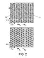
- a 2D photonic crystal is chosen as shown in Figure 2.
- This photonic crystal consists of a hexagonal lattice with a lattice constant a (distance between the center of the cylinders closest to one another) of dielectric cylinders (10) with a high refraction index (permittivity e1) and radius r on a medium (11) with a low refraction index (permittivity e2).
- the structure is periodic in the plane in which the cylinders are distributed and is described by the directions GK and GM, whereas it is constant in the direction perpendicular to the plane of periodicity.
- This photonic crystal has a forbidden band for modes with transversal magnetic polarization (TM), that is, modes with the electric field in the direction perpendicular to the plane of the crystal.
- TM transversal magnetic polarization
- This embodiment is selected for verification at microwave frequencies in the laboratory.
- the present invention could be realized in 2D crystals with square symmetry, with another transversal form of the cylinders, interchanging materials of high and low refraction index, and even using a 3D photonic crystal without losing its general characteristics.
- Figure 3 shows an example of a waveguide (12) created in the 2D photonic crystal of Figure 2 by means of suppression of a row of cylinders along the GK direction.
- the linear defect acts as a waveguide.
- a guide from coupled cavities (13) as shown in Figure 4.
- a chain of cavities is created and propagation is due to photons jumping between neighboring cavities due to overlap of the tails of the field confined to the cavity.
- d 2a along the GK direction.
- the waveguide (12) there is a TM guide mode with frequencies within the forbidden band.
- the vertical axis represents normalized frequencies in units of c/a, where c is the speed of light in vacuum.
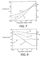
- the guide mode for the isolated guide is shown by a broken line (15), whereas the even modes (16) and odd modes (17) of the coupler are shown with a solid line.
- the transfer of power between guides of the coupler occurs in the spectral range (18) in which the even and odd modes coexist. However, we can see two spectral ranges (19) and (20) in which only the odd mode is present.
- Figure 6 shows the coupler formed by the two coupled cavity waveguides (13).
- the two guides (13) are separated by a region (14) which in this case consists of three rows of cylinders of high refraction index.
- Figure 8 shows the structure of bands of the guide modes for TM polarization of the coupled cavity waveguide (13) and the coupler of the coupled guides of Figure 6 for a separation of a row of cylinders of high refraction index in the region between the guides (14).
- Figure 7 on the vertical axis, normalized frequencies are represented in units of c/a and on the horizontal axis, the propagation constants limited to the first Brillouin zone.
- the guide mode of the isolated guide is shown with a broken line (21), and the even modes (22) and odd modes (23) of the coupler as a solid line.
- the even and odd modes are much more uncoupled from one another with respect to the bands of the coupler of Figure 5.
- the coupling is of the same order of magnitude in the longitudinal direction of the guides (GK) as in the transversal direction (GM), whereas in the coupler shown in Figure 5, coupling is much stronger in the longitudinal direction due to a smaller separation between adjacent cavities.
- GK longitudinal direction of the guides
- GM transversal direction
- coupling is much stronger in the longitudinal direction due to a smaller separation between adjacent cavities.
- coupled cavity waveguides (13) are used due to the high transmission efficiency in tight curves that this type of guide offers.
- Guides (12) can also be used for the input and output ports.
- the spectral range of operation of the divider will be the intersection between the range (24) in which only an odd mode is present (23) and the range in which one guide mode is present (21) for the input and output guides.
- the range of operation is restricted to the dotted rectangle (27) in Figure 8.
- the spectral zone (34) corresponds to the range (26) of Figure 8 where only the even mode is present, and so the power should be the same at both outputs, as observed in Figure 11, but without a phase difference between signals.
- N the number of cavities
- the responses (35) and (36) in the region (32) are very similar and show that both output ports have the same power.
- N > 1 the divider works correctly and divides the input signal into two equal-power output signals with a phase difference of 180°, and as N increases, the bandwidth will be greater as the Q parameter of zone (31) decreases.
- a forbidden band was observed between 7.36 and 11.7 GHz along the GK direction. Then, a guide was introduced like the one in Figure 4 and a guided band was observed for TM polarization between 8.53 and 9.05 GHz.
- This guided band corresponds to mode (21) in Figure 8.
- the amplitude response is shown with the solid line (37) for the output port (29) and with a broken line (38) for the output port (30).
- the phase response is shown with a solid line (39) for the output port (29) and a solid line (40) for the output port (30).
- the zone (32) is the one that corresponds to the 180° divider, and in phase response it is observed that the difference in phase between the two outputs (50) and (51) is 180° approximately over the whole range.
- the difference in amplitude response (37) and (38) in the spectral range (32) is due to imprecision in the implementation of the structure, unwanted external reflections as well as to lack of modal adaptation between the different sections of the divider.
- the range of the divider is 180° and it occupies a spectral width of around 300 MHz, that is, a relative bandwidth of 3.45 %, sufficient for numerous applications.
- a bandwidth greater than 50 nm would be obtained, suitable for applications in optical multiplex networks by division of wavelength.
- both even and odd modes are excited and there is no stable behavior of the amplitude and phase outputs.
- the region (34) would correspond to the zone of excitation of the even mode, which is confirmed if we observe the phase response of the structure where we see that (39) and (40) are in phase in this interval.
- the response in amplitude for the region (34) shows equilibrium in the output power at both ports (29) and (30).
- the total power in the excitation region of the even mode (34) is smaller than that in the excitation region of the odd mode (32) because the even mode (22) has a flatter frequency than the odd mode (23), and so greater lack of modal adaptation will occur and a lower global transmission efficiency.
Landscapes
- Physics & Mathematics (AREA)
- Engineering & Computer Science (AREA)
- Optics & Photonics (AREA)
- Microelectronics & Electronic Packaging (AREA)
- General Physics & Mathematics (AREA)
- Chemical & Material Sciences (AREA)
- Nanotechnology (AREA)
- Life Sciences & Earth Sciences (AREA)
- Biophysics (AREA)
- Crystallography & Structural Chemistry (AREA)
- Optical Integrated Circuits (AREA)
Abstract
The invention relates to a method of dividing the power of an input electromagnetic signal into two equal-power signals with a relative phase difference of 180° between them and an equal propagation delay. The inventive method makes use of a photonic crystal coupler comprising two parallel guides which are disposed close to one another and which are based on coupled cavities. The method consists in exciting the odd mode of the coupler which, owing to the symmetry thereof, ensures that the field maxima coincide in one guide with the minima in the adjacent guide, thereby producing a relative phase difference of 180°. The two output signals are obtained through the spatial separation of the guides forming the coupler, making use of the property possessed by guides in photonic crystals for high transmission efficiency through very tight curves. In this way, the size of the structure can be reduced considerably. The inventive method can be used for both two-dimensional and three-dimensional photonic crystals.
Description
- The present invention consists of a method that allows the power of an input electromagnetic signal to be divided into two equal-power signals with a relative phase difference of 180° and an equal propagation delay. This method makes use of a coupler consisting of two parallel guides disposed close to one another in a photonic crystal. Both two-dimensional (2D) and three-dimensional (3D) crystals could be used as the underlying concept is the same. The advantages of the divider structure are its small size, which makes it suitable for integration of numerous dividing units as functional units of more complex devices, the high operational bandwidth, which is an advantage with respect to other methods for dividing power which are sensitive to frequency, and synchrony between the output signals from the device, which is an essential feature for high-speed signal processing.
- The field for application of the present invention is in any device based on 2D or 3D photonic crystal technology designed to operate over any frequency range, from optical signals and microwave/millimeter signals, to signals with frequencies in the visible or infrared range.
- Photonic crystals are formed from materials with a dielectric constant that varies periodically in one, two or three spatial dimensions. This periodicity gives rise to the appearance of frequency bands in which signal propagation is not permitted inside the crystal. These forbidden frequency bands are commonly known as the Photonic Band Gap (PBG). Light propagation can be controlled by inserting defects that alter the periodicity of the crystal. The insertion of linear defects leads to the appearance of guided modes at frequencies within the forbidden band allowing the propagation of light only in the defect created. Although total control of the propagation of light is achieved by using 3D photonic crystals, control of light in three dimensions can also be achieved with planar 2D photonic crystals, thus reducing the cost and complexity of manufacture. In this case, the light is confined to the direction perpendicular to the plane of the crystal if the dielectric constant of the materials above and below the crystal is less than the dielectric constant of the defect created in the crystal. The main advantages of the devices based on photonic crystals are a considerable reduction in size, allowing highly integrated optical circuits to be produced, and the possibility of implementing curved guides with radii of the order of the wavelength of the signal that is being propagated without significant losses, which is essential for the development of microphotonics.
- Due to the scaling properties of Maxwell's equations, photonic crystals can be made to have a forbidden band in any spectral range provided the structure is appropriately scaled and provided materials are chosen that have suitable properties in the chosen spectral range. As it is extremely costly to manufacture structures in the visible or infrared frequencies, in which the spatial periodicity should be less than one micron, photonic crystals have been implemented to work at microwave frequencies where the periodicity is of the order of cm. To do this, bars of dielectric material with a high refraction index are used that form periodic lattices in air. The properties of these structures can by and large be extrapolated to the structures corresponding to optical frequencies, but with the advantage that at microwave frequencies, manufacture and measurement of the properties is much easier.
- In a photonic crystal, a waveguide can be created from a chain of equally spaced cavities or point defects along a certain direction of the crystal. This type of guide is known as a coupled cavity waveguide. The propagation along these guides is explained by photons jumping between adjacent cavities due to overlap of the evanescent field tails. The coupled cavity waveguides have certain characteristics that make them particularly interesting: on the one hand, a theoretical expression can be derived for the dispersion ratio of the guide modes from tight-binding approach used in solid-state physics. On the other hand, transmission along curves with very tightly curved radii is very efficient provided that symmetry of the cavity mode is appropriate. In addition, the group velocity of this type of guide is very low, tending to zero at the edges of the band, and so highly efficient non-linear processes are expected in this type of guide, as well as high dispersion that could be of use in a number of applications.
- On the other hand, couplers in photonic crystal technology can be implemented in the same way as used by other more mature technologies, such as integrated guides or fiber optics: disposing two parallel wave guides close to one another. If both guides are identical and single moded when placed in proximity, the two interact and the guide mode of an isolated guide divides into two modes for the complete system of the two parallel waveguides. These modes have even and odd symmetry with respect to the plane equidistant from the guide axis. In addition, these modes have different propagation constants, implying that they travel at a different velocity along the coupler. This behavior causes a signal to be excited in one of the two guides, after a certain distance the wave passes to the adjacent guide and, once again, returns to the original guide after covering the same distance. That is, there is a periodic transfer of power between guides. In 2D photonic crystals, couplers have been proposed and studied formed from guides made by completely eliminating a row of cylinders in dielectric cylinder structures over air. The performance of a directional coupler has also been shown experimentally at optical frequencies in a planar photonic crystal with air holes on a silicon substrate. In addition, a coupler has been proposed in a 2D photonic crystal of air holes in dielectric for commutation applications.
- The power dividers/combiners are fundamental blocks in any optical network or device. Their function is to distribute the power of an input signal to two output ports with certain percentages at each output. If the percentages are 50%, the divider is usually called a 3 dB divider. These blocks can be implemented mainly in two ways (see Figures 1a and 1b): either using a directional coupler designed such that the power is divided equally between the output ports at on output (Figure 1a), or by means of a Y-shaped structure in which the input guide divides into two output guides at a certain angle to minimize losses (Figure 1b). For the first case, the phase difference between the output signals is 90% whereas for the second case, both outputs are in phase. In addition to couplers, the implementation of Y-shaped dividers has also been proposed in photonic crystal technology and it has been demonstrated experimentally at both microwave and optical frequencies.
- The invention relates to a method of dividing the power of an input electromagnetic signal into two equal-power signals with a relative phase difference between the two of 180° and an equal propagation delay. The structure can also be designed so that the phase difference between output signals is 0° although, whatever the phase difference, the output signals travel the same physical path and are in synchrony.
- Said method makes use of a coupler implemented in a photonic crystal and consisting of two parallel guides located close to one another and based on coupled cavities.
- The physical basis of the proposed method is based on exciting the odd mode of the coupler, which because of its symmetry, ensures that field maxima in one guide coincide with minima in the adjacent guide so achieving a relative phase difference of 180 degrees. The two output signals are obtained by spatial separation of the guides that make up the coupler, making use of the property that possess the guides in photonic crystals of high transmission efficiency through tight curves, a property which allows the size of the structure to be considerably reduced.
- The method is valid both for two-dimensional (2D) and three-dimensional (3D) photonic crystals as the underlying concept is the same.
- The advantages of the divider structure are its small size, which makes it suitable for integration of several dividing units as functional units of more complex devices, large bandwidth, and synchronization of the two output signals of the structure, which allows high-speed signal processing.
- By means of the same method, a divider could be obtained with the output signals in-phase if, instead of odd mode, the even mode of the coupler is used.
- The photonic crystal comprises a lattice of cylinders grouped in columns that can adopt any value for the lattice constant (distance between cylinders closest to one another), was well as any radius and height of the cylinders. Likewise, the method is applicable for any difference of refraction indexes between the material of the columns, the material that surrounds the columns and the material above and below the crystal.
- The photonic crystals can adopt any type of lattice, particularly a triangular lattice or square lattice.
- The dielectric guide can have any type of configuration to create the coupler, (width and height of the nucleus and layers that surround it), was well as any refraction index, including also the optical fiber.
- The method is likewise applicable to any type of guide in a photonic crystal that is used to inject and extract signals from the coupling region.
- To complement the description being made and in order to facilitate a better understanding of the characteristics of the invention, in accordance with a preferred example of a practical embodiment thereof, as an integral part of such description, a set of figures is included in which, for illustrative purposes, and in no way limiting, the following has been represented:
- Figures 1a and 1b show the most widely used structures in optical circuits for dividing the power of an input signal at two output ports: Figure 1a shows a directional coupler in which a periodic transfer of power occurs between guides such that, with an appropriate selection of the length of the coupler, a certain ratio of powers can be obtained at the output ports. Figure 1b shows a Y-shaped divider in which the input guide divides into two output guides such that both carry the same power.
- Figure 2 schematically represents a 2D photonic crystal with hexagonal symmetry and periodic structure in the GK and GM directions, whereas it remains invariant in the direction perpendicular to the plane of periodicity.
- Figure 3 shows a waveguide created in the photonic crystal shown in Figure 2 by eliminating a row of columns of high index in the GK direction.
- Figure 4 shows a coupled cavity waveguide created in the photonic crystal shown in Figure 2 by eliminating every second column of high index in the GK direction.
- Figure 5 shows a coupler created in the photonic crystal shown in Figure 2 consisting of two guides such as those shown in Figure 3 that are parallel and separated by three rows of cylinder of high index.
- Figure 6 shows a coupler of coupled cavity waveguides created in the photonic crystal shown in Figure 2.
- Figure 7 shows the band structure of the modes guided with TM polarization of a guide such as that shown in Figure 3 (broken line) and a coupler such as the one shown in Figure 5.
- Figure 8 shows the band structure of the guide modes with TM polarization of coupled cavities such as the one shown in Figure 4 (broken line) and a coupler of coupled cavity waveguides (solid line) such as the one shown in Figure 6 and which constitutes the coupling section of Figure 9.
- Figure 9 shows the schematic of a possible embodiment of the present invention: the central part of the structure, highlighted in the broken rectangle in Figure 9, shows the coupling section that is made up of a coupler of coupled cavity waveguides consisting of N cavities (specifically N = 5) such as the one shown in Figure 6.
- Figure 10 shows the electric field pattern parallel to the axis of the cylinders for a monochromatic wave of normalized frequency 0.44 c/a, where c is the speed of light in vacuum (within the operating range of the coupler) which is injected into the power divider structure shown in Figure 9.
- Figure 11 shows the power transmission spectrum of the preferred embodiment of the structure shown in Figure 9 for the particular cases N = 4 and N = 6.
- Figure 12 shows the experimental response in amplitude (a) and phase (b) of the preferred embodiment using 300 cylinders of alumina with a = 1.5 cm.
- Figure 1 shows the two structures that are widely used in optical circuits to divide the power of an input signal at two output ports: Figure 1a shows the directional coupler formed from two equal parallel guides close to one another in which periodic transfer of power between guides occurs in the coupling region (4) such that with suitable selection of the length of the coupler, it is possible to obtain a certain ratio of powers at the output ports (2)-(3). If this ratio is 50% for each port, that is, the power of the input signal (1) is evenly distributed between the output ports (2)-(3), the relative phase difference between the two is 90°. At the input port (5), power is not introduced. Because coupling depends on frequency, exact 50% division only occurs for one frequency, although in the spectral range either side of this frequency, it will be close to 50%. Figure 1 b shows a Y-shaped divider in which the input guide (6) divides into two output guides (8)-(9) such that both channel the same power. The angle of the output guides should be designed in order to maximize the power at each of the output guides. The area of division (7) should also be suitable designed. Both structures can be implemented with 2D and 3D photonic crystal technology. These two structures are described in order to subsequently compare them with the invention that is detailed here and to show the advantages that the present invention has with respect to these structures.
- In order to describe the present invention and offer results that verify the behavior, as a preferred embodiment, a 2D photonic crystal is chosen as shown in Figure 2. This photonic crystal consists of a hexagonal lattice with a lattice constant a (distance between the center of the cylinders closest to one another) of dielectric cylinders (10) with a high refraction index (permittivity e1) and radius r on a medium (11) with a low refraction index (permittivity e2). The structure is periodic in the plane in which the cylinders are distributed and is described by the directions GK and GM, whereas it is constant in the direction perpendicular to the plane of periodicity. This photonic crystal has a forbidden band for modes with transversal magnetic polarization (TM), that is, modes with the electric field in the direction perpendicular to the plane of the crystal. This embodiment is selected for verification at microwave frequencies in the laboratory. However, the present invention could be realized in 2D crystals with square symmetry, with another transversal form of the cylinders, interchanging materials of high and low refraction index, and even using a 3D photonic crystal without losing its general characteristics.
- Figure 3 shows an example of a waveguide (12) created in the 2D photonic crystal of Figure 2 by means of suppression of a row of cylinders along the GK direction. On creating the guide, there is a mode with TM polarization confined to the linear defect with frequencies within the forbidden band, and so the linear defect acts as a waveguide. It is also possible to create a guide from coupled cavities (13) as shown in Figure 4. In this case, a chain of cavities is created and propagation is due to photons jumping between neighboring cavities due to overlap of the tails of the field confined to the cavity. In the particular case of Figure 4, the cavities are created by eliminating a high refractive index cylinder and the separation between them is d = 2a along the GK direction. Similarly, for the waveguide (12), there is a TM guide mode with frequencies within the forbidden band.
- If two wave guides (12) are located close together in the 2D photonic crystal as shown in Figure 5, a coupler is obtained. Due to the proximity of the guides (12) the mode of an isolated guide splits into two modes for the coupler with even and odd symmetry with respect to the plane equidistant from the axes of the parallel guides (12). These modes have different propagation constants, which because of the periodicity of the structure in the direction of the guides, are limited to the first Brillouin zone. Figure 7 shows the structure of the bands for modes with TM polarization (12) described in Figure 3 and of the modes of the coupler described in Figure 5 for a separation of one cylinder between guides in the separation region (14). The vertical axis represents normalized frequencies in units of c/a, where c is the speed of light in vacuum. The guide mode for the isolated guide is shown by a broken line (15), whereas the even modes (16) and odd modes (17) of the coupler are shown with a solid line. For the preferred embodiment, the parameters chosen are: e1 = 10.3, e2 = 1, r = 0.133a. The transfer of power between guides of the coupler occurs in the spectral range (18) in which the even and odd modes coexist. However, we can see two spectral ranges (19) and (20) in which only the odd mode is present. We can use this range in which only the odd mode exists to create a power divider, as the signal will travel along the two guides with a phase difference of 180° and be of equal power because of the odd symmetry. However, because the coupled cavity waveguides (13) have better transmission properties along tight curves than the guides (12), which is extremely important when introducing and extracting signals as will be seen a posteriori, for the preferred embodiment the structure shown in Figure 6 will be used, although the underlying concept for the invention that is detailed here is exactly the same: excite the odd mode of the coupler in the photonic crystal in a spectral region in which only this mode is present and spatially separate at the output the two guides that comprise the coupler to obtain two equal-power signals with a phase difference of 180°.
- Figure 6 shows the coupler formed by the two coupled cavity waveguides (13). The two guides (13) are separated by a region (14) which in this case consists of three rows of cylinders of high refraction index. Figure 8 shows the structure of bands of the guide modes for TM polarization of the coupled cavity waveguide (13) and the coupler of the coupled guides of Figure 6 for a separation of a row of cylinders of high refraction index in the region between the guides (14). As in Figure 7, on the vertical axis, normalized frequencies are represented in units of c/a and on the horizontal axis, the propagation constants limited to the first Brillouin zone. The guide mode of the isolated guide is shown with a broken line (21), and the even modes (22) and odd modes (23) of the coupler as a solid line. Here, it is observed that the even and odd modes are much more uncoupled from one another with respect to the bands of the coupler of Figure 5. This is due to the fact that in the coupler of Figure 6, the coupling is of the same order of magnitude in the longitudinal direction of the guides (GK) as in the transversal direction (GM), whereas in the coupler shown in Figure 5, coupling is much stronger in the longitudinal direction due to a smaller separation between adjacent cavities. Thus, we have a large spectral region (24) in which only the odd mode exists and which can be used to implement the power divider with a phase difference of 180°. The spectral region where only the even mode is present (26) is not as wide, and the region where both modes coexist is almost indiscernible (25) due to extensive uncoupling. These are the results for the preferred embodiment, but a design could be drawn up in which the even and odd modes did not coexist in frequency and the whole of the region of the odd mode (23) would be available to implement the divider.
- From the results presented earlier, the method is presented for dividing electromagnetic signals with a phase difference of 180° between outputs. This method is described in the structure shown in Figure 9 for the particular case of the preferred embodiment, for which the values of the parameters used previously are maintained. The central part of the divider structure (31) is a coupler of coupled cavity waveguides as shown in Figure 6, with a separation of a row of cylinders in the region (14). In the particular case of Figure 9, it is comprised of N = 5 cavities along the direction of propagation. To enter the divider structure (31), in this particular embodiment coupled cavity waveguides (13) are used due to the high transmission efficiency in tight curves that this type of guide offers. Thus, there is an input coupled cavity waveguide (28) and two output coupled cavity waveguides (29) and (30). Guides (12) can also be used for the input and output ports. The spectral range of operation of the divider will be the intersection between the range (24) in which only an odd mode is present (23) and the range in which one guide mode is present (21) for the input and output guides. Thus, the range of operation is restricted to the dotted rectangle (27) in Figure 8.
- In order to verify the nature of the power divider and 180° phase-shifting of the proposed method, in Figure 10 a simulation is shown with a method of finite differences in the time domain of the electric field distribution parallel to the axis of the cylinders for a monochromatic wave with a normalized frequency 0.44 (which lies in the operating range of the ). On introducing this signal into the input port (28), the signal reaches the section of the coupler that, in this case, consists of N = 6 cavities, and excites the odd mode. The field maxima are shown in white shades and the minima in black shades. It is observed that in the region of coupling, the maxima of one of the guides correspond to minima with the adjacent one, and vice versa, which confirms that the exciting mode is of odd symmetry. At the output, use is made of the property of spatial periodicity of the 2D photonic crystal to divide the guides of the coupler into two output points (29) and (30). The odd symmetry is maintained at the output ports, and so the phase difference between them is 180°. In addition, the path covered by the two signals through the structure is identical and so they are synchronized. This property is very important, as high speed signals can be used without delays at the outputs. If, for example, it is desired to implement a divider with a phase difference of 180° from a divider with a difference of 90°, this could be done by adding an additional path in one of the output ports that adds an extra phase difference of 90°. However, this mechanism will also add to the propagation delay and so the condition of synchrony between output signals would not be met, unlike the proposed method.
- In order to analyze the frequency behavior of the divider, a power transmission spectrum is obtained at both outputs by means of a simulation with a finite differences method in the time domain. The results are shown in Figure 11, for two particular cases of length of coupler: N = 4 (35) and N = 6 (36). The response (36) is shifted 30 dB downwards for better visualization. The solid line is the response for output (30) and the broken line for output (29) in Figure 10. Three spectral ranges are observed of different behavior in the structure: (32), (33) and (34). In the range (32), both outputs have the same power, which confirms that the structure behaves as a power divider. The fact that the output power is not constant over frequency is because of the contribution from spurious reflections due to lack of modal adaptation between the different sections of the structure. Comparing with Figure 8, we can say that the range (32) corresponds to the operating range of the divider. This is then the spectral range of interest and the range over which the present invention operates. Other spectral regions (33) and (34) are commented below to check the validity of the above description of the structure shown in Figure 9. The zone (33) corresponds to the range (25) of Figure 8 where both even and odd modes are excited. In this case, the power at both output ports does not have to be the same, as can be seen in zone (33). On the other hand, the spectral zone (34) corresponds to the range (26) of Figure 8 where only the even mode is present, and so the power should be the same at both outputs, as observed in Figure 11, but without a phase difference between signals. With regard to the influence of the number of cavities N that make up the cavity, we can say that it does not have much effect, and the responses (35) and (36) in the region (32) are very similar and show that both output ports have the same power. In principle, the divider works well from N = 2 onwards, because, for N = 1, the output guides (29) and (30) are very close to the input guide (28) and the zone (31) does not act as a coupler. For N > 1, the divider works correctly and divides the input signal into two equal-power output signals with a phase difference of 180°, and as N increases, the bandwidth will be greater as the Q parameter of zone (31) decreases.
- The simulation method available does not allow phase measurements to be obtained and so the divider shown in Figure 9 was implemented in the laboratory using 300 bars of alumina with constant e1 = 10.3,
height 10 cm andradius 2 mm. To generate signals and perform the measurements of amplitude and phase, a vectorial network analyzer was used of up to 50 GHz. For r = 0.133a as in the simulations, a = 1.5 cm was chosen. For the defect-free crystal, as shown in Figure 2 and for a TM polarized signal, a forbidden band was observed between 7.36 and 11.7 GHz along the GK direction. Then, a guide was introduced like the one in Figure 4 and a guided band was observed for TM polarization between 8.53 and 9.05 GHz. This guided band corresponds to mode (21) in Figure 8. Afterwards, the divider shown in Figure 9 with N = 4 cavities was introduced and transmission measurements were made of amplitude and phase that are shown in Figure 12. The amplitude response is shown with the solid line (37) for the output port (29) and with a broken line (38) for the output port (30). The phase response is shown with a solid line (39) for the output port (29) and a solid line (40) for the output port (30). Also shown are the three spectral regions (32), (33) and (34) of differing behavior of the divider already included in Figure 11. The zone (32) is the one that corresponds to the 180° divider, and in phase response it is observed that the difference in phase between the two outputs (50) and (51) is 180° approximately over the whole range. The difference in amplitude response (37) and (38) in the spectral range (32) is due to imprecision in the implementation of the structure, unwanted external reflections as well as to lack of modal adaptation between the different sections of the divider. The range of the divider is 180° and it occupies a spectral width of around 300 MHz, that is, a relative bandwidth of 3.45 %, sufficient for numerous applications. By way of a simple example, in the optical band of 1550 nm, used in optical communications, a bandwidth greater than 50 nm would be obtained, suitable for applications in optical multiplex networks by division of wavelength. In the range (33), both even and odd modes are excited and there is no stable behavior of the amplitude and phase outputs. Finally, the region (34) would correspond to the zone of excitation of the even mode, which is confirmed if we observe the phase response of the structure where we see that (39) and (40) are in phase in this interval. The response in amplitude for the region (34) shows equilibrium in the output power at both ports (29) and (30). The total power in the excitation region of the even mode (34) is smaller than that in the excitation region of the odd mode (32) because the even mode (22) has a flatter frequency than the odd mode (23), and so greater lack of modal adaptation will occur and a lower global transmission efficiency.
Claims (7)
- Method of dividing a guided electromagnetic signal into two half-power signals using photonic crystals characterized in that it is based on exciting a coupler made by disposing two parallel coupled cavity waveguides close to one another, implemented in photonic crystals, in which the two guides are physically separated and can be suitably curved to extract the two output signals, output signals that cover the same physical path and so there is no delay between the two.
- Method of dividing a guided electromagnetic signal into two half-power signals using photonic crystals according to Claim 1, characterized in that it is based on exciting the odd mode of the coupler obtaining at the output two signals with a 180° phase difference.
- Method of dividing a guided electromagnetic signal into two half-power signals using photonic crystals according to Claim 1, characterized in that it is based on exciting the even mode of the coupler designed with greater bandwidth obtaining at the output two signals in phase.
- Method of dividing a guided electromagnetic signal into two half-power signals using photonic crystals according to Claims 1, 2 and 3, characterized in that it can use any type of 2D crystal.
- Method of dividing a guided electromagnetic signal into two half-power signals using photonic crystals according to Claims 1, 2 and 3, characterized in that it can use any type of 3D crystal.
- Method of dividing a guided electromagnetic signal into two half-power signals using photonic crystals according to Claims 1, 4 and 5, characterized in that it is for application in a photonic crystal with a triangular lattice type.
- Method of dividing a guided electromagnetic signal into two half-power signals using photonic crystals according to Claims 1, 4 and 5, characterized in that it is for application in a photonic crystal with a square lattice type.
Applications Claiming Priority (2)
| Application Number | Priority Date | Filing Date | Title |
|---|---|---|---|
| ES200302003A ES2229918B1 (en) | 2003-08-14 | 2003-08-14 | METHOD FOR DIVIDING A GUIDED ELECTROMAGNETIC SIGNAL IN TWO SIGNS WITH HALF OF POWER USING PHOTONIC CRYSTALS. |
| PCT/ES2004/000378 WO2005017586A1 (en) | 2003-08-14 | 2004-08-14 | Method of dividing a guide electromagnetic signal into two half-power signals, using photonic crystals |
Publications (1)
| Publication Number | Publication Date |
|---|---|
| EP1677130A1 true EP1677130A1 (en) | 2006-07-05 |
Family
ID=34178762
Family Applications (1)
| Application Number | Title | Priority Date | Filing Date |
|---|---|---|---|
| EP04766917A Withdrawn EP1677130A1 (en) | 2003-08-14 | 2004-08-14 | Method of dividing a guide electromagnetic signal into two half-power signals, using photonic crystals |
Country Status (5)
| Country | Link |
|---|---|
| US (1) | US7433562B2 (en) |
| EP (1) | EP1677130A1 (en) |
| JP (1) | JP2007534002A (en) |
| ES (1) | ES2229918B1 (en) |
| WO (1) | WO2005017586A1 (en) |
Cited By (1)
| Publication number | Priority date | Publication date | Assignee | Title |
|---|---|---|---|---|
| EP3333605A1 (en) * | 2016-12-07 | 2018-06-13 | Hitachi Ltd. | Photonic device |
Families Citing this family (4)
| Publication number | Priority date | Publication date | Assignee | Title |
|---|---|---|---|---|
| US20130058611A1 (en) * | 2011-09-01 | 2013-03-07 | Feng Shi | Photonic crystal optical waveguide solar spectrum splitter |
| CN104678492B (en) * | 2015-02-26 | 2017-05-24 | 南京邮电大学 | Mode division multiplexing and de-multiplexing device based on photonic crystal |
| US10859769B2 (en) * | 2018-09-06 | 2020-12-08 | Mitsubishi Electric Research Laboratories, Inc. | Compact photonic devices |
| CN114665236B (en) * | 2022-02-25 | 2025-07-22 | 深圳市朗赛微波通信有限公司 | Multipath polarization coupler |
Family Cites Families (7)
| Publication number | Priority date | Publication date | Assignee | Title |
|---|---|---|---|---|
| JP3325825B2 (en) * | 1997-03-29 | 2002-09-17 | 彰二郎 川上 | Three-dimensional periodic structure, method for producing the same, and method for producing film |
| US6101300A (en) * | 1997-06-09 | 2000-08-08 | Massachusetts Institute Of Technology | High efficiency channel drop filter with absorption induced on/off switching and modulation |
| US6130969A (en) * | 1997-06-09 | 2000-10-10 | Massachusetts Institute Of Technology | High efficiency channel drop filter |
| EP1315987A4 (en) * | 2000-08-15 | 2005-06-29 | Corning Inc | Active photonic crystal waveguide device |
| JP2002323631A (en) * | 2001-04-24 | 2002-11-08 | Sumitomo Heavy Ind Ltd | Method and apparatus for manufacturing microdevice |
| AU2003231080A1 (en) * | 2002-04-25 | 2003-11-10 | Massachusetts Institute Of Technology | Optimal bistable switching in non-linear photonic crystals |
| FR2841658B1 (en) | 2002-06-26 | 2004-10-22 | Centre Nat Rech Scient | WAVELENGTH SELECTIVE AND DIRECTIONAL OPTICAL COUPLING DEVICE |
-
2003
- 2003-08-14 ES ES200302003A patent/ES2229918B1/en not_active Expired - Fee Related
-
2004
- 2004-08-14 JP JP2006523023A patent/JP2007534002A/en active Pending
- 2004-08-14 EP EP04766917A patent/EP1677130A1/en not_active Withdrawn
- 2004-08-14 WO PCT/ES2004/000378 patent/WO2005017586A1/en not_active Ceased
- 2004-08-14 US US10/568,363 patent/US7433562B2/en not_active Expired - Fee Related
Non-Patent Citations (1)
| Title |
|---|
| See references of WO2005017586A1 * |
Cited By (1)
| Publication number | Priority date | Publication date | Assignee | Title |
|---|---|---|---|---|
| EP3333605A1 (en) * | 2016-12-07 | 2018-06-13 | Hitachi Ltd. | Photonic device |
Also Published As
| Publication number | Publication date |
|---|---|
| JP2007534002A (en) | 2007-11-22 |
| ES2229918B1 (en) | 2006-08-16 |
| ES2229918A1 (en) | 2005-04-16 |
| WO2005017586A1 (en) | 2005-02-24 |
| US20060171634A1 (en) | 2006-08-03 |
| US7433562B2 (en) | 2008-10-07 |
Similar Documents
| Publication | Publication Date | Title |
|---|---|---|
| Ghaffari et al. | Analysis of photonic crystal power splitters with different configurations | |
| Orazbayev et al. | Chiral waveguides for robust waveguiding at the deep subwavelength scale | |
| Wang et al. | Channel drop filters with folded directional couplers in two-dimensional photonic crystals | |
| Jiu-Sheng et al. | Compact four-channel terahertz demultiplexer based on directional coupling photonic crystal | |
| Mohammadi et al. | Optimization and realization all-optical compact five-channel demultiplexer using 2D photonic crystal based hexagonal cavities | |
| Danaie et al. | Design of adjustable T-shaped and Y-shaped photonic crystal power splitters for TM and TE polarizations | |
| Dhandrapati et al. | A novel 8-channel DWDM demultiplexer on silicon photonic crystal slab: Design and analysis | |
| Ghaffari et al. | Photonic crystal power splitter and wavelength multi/demultiplexer based on directional coupling | |
| US7433562B2 (en) | Method of dividing a guided electromagnetic signal into two half-power signals using photonic crystals | |
| Jin et al. | Reflectionless multichannel wavelength demultiplexer in a transmission resonator configuration | |
| Haxha et al. | Analysis of wavelength demultiplexer based on photonic crystals | |
| Saral et al. | Two-dimensional photonic crystal based compact power splitters | |
| Balaji et al. | Design and analysis of waveguide taper for photonic crystal demultiplexer | |
| Liu et al. | Channel-drop filters in three-dimensional woodpile photonic crystals | |
| Lu et al. | Wavelength routers with low crosstalk using photonic crystal point defect micro-cavities | |
| Mohammadi et al. | Five-port power splitter based on pillar photonic crystal | |
| Martinez et al. | Photonic-crystal 180° power splitter based on coupled-cavity waveguides | |
| Badaoui et al. | Photonic-crystal band-pass resonant filters design using the two-dimensional FDTD method | |
| Jindal et al. | Different configurations of photonic crystal power splitters for PIC’s—a review | |
| Fan et al. | Manipulating light with photonic crystals | |
| Rakshitha et al. | Photonic Crystal Ring resonator based 1x4 Optical power splitter | |
| Radhouene et al. | Design and analysis of a channel drop filter and demultiplexer based on a photonic crystal super ellipse-shaped ring resonator | |
| Jindal et al. | Design and Optimization of 2D Photonic Crystal Based Compact All Optical T Splitter for Photonic Integrated Circuits | |
| Bazargani et al. | Design of optical 2-channel demultiplexer using selective optofluidic infiltration within photonic crystal structure | |
| Icli et al. | Numerical and experimental demonstration of inverse designed low-index polarization-insensitive wavelength demultiplexer |
Legal Events
| Date | Code | Title | Description |
|---|---|---|---|
| PUAI | Public reference made under article 153(3) epc to a published international application that has entered the european phase |
Free format text: ORIGINAL CODE: 0009012 |
|
| 17P | Request for examination filed |
Effective date: 20060309 |
|
| AK | Designated contracting states |
Kind code of ref document: A1 Designated state(s): AT BE BG CH CY CZ DE DK EE ES FI FR GB GR HU IE IT LI LU MC NL PL PT RO SE SI SK TR |
|
| DAX | Request for extension of the european patent (deleted) | ||
| STAA | Information on the status of an ep patent application or granted ep patent |
Free format text: STATUS: THE APPLICATION IS DEEMED TO BE WITHDRAWN |
|
| 18D | Application deemed to be withdrawn |
Effective date: 20100302 |