EP1675222A1 - Connection terminal and connector equipped therewith - Google Patents
Connection terminal and connector equipped therewith Download PDFInfo
- Publication number
- EP1675222A1 EP1675222A1 EP05292777A EP05292777A EP1675222A1 EP 1675222 A1 EP1675222 A1 EP 1675222A1 EP 05292777 A EP05292777 A EP 05292777A EP 05292777 A EP05292777 A EP 05292777A EP 1675222 A1 EP1675222 A1 EP 1675222A1
- Authority
- EP
- European Patent Office
- Prior art keywords
- face
- substrate
- spring contact
- connection terminal
- card edge
- Prior art date
- Legal status (The legal status is an assumption and is not a legal conclusion. Google has not performed a legal analysis and makes no representation as to the accuracy of the status listed.)
- Granted
Links
Images






Classifications
-
- H—ELECTRICITY
- H01—ELECTRIC ELEMENTS
- H01R—ELECTRICALLY-CONDUCTIVE CONNECTIONS; STRUCTURAL ASSOCIATIONS OF A PLURALITY OF MUTUALLY-INSULATED ELECTRICAL CONNECTING ELEMENTS; COUPLING DEVICES; CURRENT COLLECTORS
- H01R12/00—Structural associations of a plurality of mutually-insulated electrical connecting elements, specially adapted for printed circuits, e.g. printed circuit boards [PCB], flat or ribbon cables, or like generally planar structures, e.g. terminal strips, terminal blocks; Coupling devices specially adapted for printed circuits, flat or ribbon cables, or like generally planar structures; Terminals specially adapted for contact with, or insertion into, printed circuits, flat or ribbon cables, or like generally planar structures
- H01R12/70—Coupling devices
- H01R12/71—Coupling devices for rigid printing circuits or like structures
- H01R12/72—Coupling devices for rigid printing circuits or like structures coupling with the edge of the rigid printed circuits or like structures
- H01R12/721—Coupling devices for rigid printing circuits or like structures coupling with the edge of the rigid printed circuits or like structures cooperating directly with the edge of the rigid printed circuits
-
- H—ELECTRICITY
- H01—ELECTRIC ELEMENTS
- H01R—ELECTRICALLY-CONDUCTIVE CONNECTIONS; STRUCTURAL ASSOCIATIONS OF A PLURALITY OF MUTUALLY-INSULATED ELECTRICAL CONNECTING ELEMENTS; COUPLING DEVICES; CURRENT COLLECTORS
- H01R13/00—Details of coupling devices of the kinds covered by groups H01R12/70 or H01R24/00 - H01R33/00
- H01R13/02—Contact members
- H01R13/10—Sockets for co-operation with pins or blades
- H01R13/11—Resilient sockets
- H01R13/113—Resilient sockets co-operating with pins or blades having a rectangular transverse section
Definitions
- the present invention relates to a connection terminal which can electrically connect an electric wiring with conductor areas of a substrate and also relates to a connector equipped therewith.
- a tuning-fork type contact, a bellows type contact, a cantilever-type contact and others have been used inside these connectors as a connection terminal for providing an electrical connection.
- one end of a tuning-fork type contact is used to hold the cable and the other end of the tuning-fork type contact is inserted into a through hole of the substrate, thereby making it possible to electrically connect the cable with the substrate.
- Japanese Published Unexamined Patent Application No. H11-185898 has disclosed a right angle connector in which contacts can be attached by press-fitting into through holes of a substrate without buckling and connected to the substrate more reliably.
- Japanese Published Unexamined Patent Application No. 2000-113928 has disclosed a connector in which a locator is used to arrange contacts more accurately and simplify positioning, so that the connector can be assembled more effectively and produced at a lower cost.
- Japanese Published Unexamined Patent Application No. 2001-6771 has disclosed a connector in which connection terminals can be arranged more accurately and flatness can be improved which is necessary for attaching by press-fitting the connection terminals into a substrate.
- connection terminals are placed on a substrate, the connectors are made greater in height when actually mounted on the substrate. Further, the manufacturing cost is increased because of attaching by press-fitting connection terminals into through holes formed on the substrate.
- the connectors disclosed in the above documents can be used for a prolonged period of time in a desirable environment, for example, in a room.
- a desirable environment for example, in a room.
- resin used for retaining a contact may be deteriorated due to a heat cycle derived from use or vibration, heat and other factors from the environment.
- a fixed end of the connection terminal retained by resin is set free and makes an electrical connection unstable.
- An object of the present invention is to provide a connection terminal, which can be made lower in height and can attain an electrical connection without fail even in an environment which produces vibration and heat and also to provide a connector equipped therewith
- connection terminal of the present invention is a connection terminal which connects an electric wiring with a substrate, comprising a crimping part which connects the electric wiring by gripping the conductor part of the electric wiring, a holding part which holds the substrate and also electrically connects conductor areas at a spring contact part which energizes the conductor areas provided at an end part of the substrate and a box part having an approximately rectangular cross section which supports the holding part and electrically communicates with the crimping part.
- the connection terminal of the present invention includes a crimping part, a holding part and a box part.
- the conductor part of an electric wiring is attached by crimping the crimping part, conductor areas fixed on an end part of a substrate are energized by a spring contact part of the holding part, thereby providing an electrical connection.
- the holding part is supported by the box part, and the crimping part is electrically connected with the box part.
- connection terminal is structured so as to hold the substrate by the holding part, thereby making it possible to partially reduce the height of the connection terminal by taking advantage of the thickness of the substrate. As a result, it can be made lower in height and smaller in size. Further, since the holding part is electrically connected with the crimping part via the box part, it is possible to electrically connect the conductor areas of the substrate with the conductor part of the electric wiring without fail.
- connection terminal is provided with the holding part and the box part, the fixed end of the connection terminal is not set free and an electrical connection is not made unstable even if resin for retaining the contact (connection terminal) is deteriorated by heat cycle through use or by vibration, heat and other factors coming from a surrounding environment.
- the holding part may additionally include a foreign matter prevention part which prevents foreign matter from entering into the spring contact part.
- the holding part may additionally include a collision avoidance part which prevents collision of the spring contact part with an end part of the substrate when the substrate is inserted and fitted.
- the box part having an approximately rectangular cross section includes in sequence a first face, a second face, a third face, a fourth face and a fifth face which are made by bending a plane member, wherein the back of the fifth face is superimposed on the surface of the first face, an end part of the first face is engaged with a clearance formed between the bent part of the fourth face and that of the fifth face, the spring contact part of the holding part is formed integrally with the first face, and the supporting part is formed integrally on the third face opposing the first face.
- the approximately rectangular cross section can be made strong by formations of the first face through the fourth face.
- the spring contact part is formed integrally on the first face and the surface of the first face is superimposed on the back of the fifth face, it is possible to protect the spring contact part by the fifth face and also prevent deformation of the spring contact part by an external impact.
- the supporting part which supports a substrate is formed integrally on the third face opposing the first face, it is possible to impart an energizing force of the spring contact part to the substrate without fail. As a result, the substrate can be secured to electrically conduct to an electric wiring via the connection terminal.
- the second face and the fourth face may communicate with the third face and include a supporting-part retaining rib for retaining a supporting part formed on the third face, the fourth face may communicate with the fifth face to retain the fifth face and include a first spring contact part protection rib for protecting the spring contact part of the first face, and the fifth face may include a second spring contact part protection rib for protecting the spring contact part formed on the first face.
- the supporting part formed on the third face is retained by the supporting-part retaining rib fixed on the second face and the fourth face.
- the spring contact part is protected by the first spring contact part protection rib provided on the fourth face and the second spring contact part protection rib provided on the fifth face.
- the fifth face may include a spring contact part protection face for protecting the spring contact part by partially bending the fifth face.
- the spring contact part is protected by the spring contact part protection face.
- strength of the supporting part is improved and the spring contact part is protected, thereby making it possible to impart an energizing force of the spring contact part to the substrate more assuredly.
- connection terminal may be formed by bending a sheet of a member.
- the thus formed connection terminal is less likely to vary in dimension of members or produce a clearance than in a case where it is formed with a plurality of members, thereby making it possible to improve the strength of the connection terminal itself and consequently improve the strength of the approximately rectangular cross section of the box part. Therefore, strength of the holding part can be kept high.
- connection terminal is constituted with a sheet of a member, it is possible to reduce the manufacturing cost as compared with a case where a plurality of members are used to manufacture connection terminals.
- Such a connector may be acceptable in which a connection terminal according to any one of Claims 1 to 7 is retained in a housing.
- connection terminal can retain the substrate by itself and provide an electric conduction, the electric conduction can be secured even when a material of the connector is deteriorated in an environment whichproduces vibration, heat, etc. As a result, a connector is available which has durability, is resistant toweather, heat and vibration. Further, since a connection terminal is used to hold a substrate, the height of the connector can be reduced by taking advantage of the thickness of the substrate, thereby making it possible to make the connector smaller in size and lower in height.
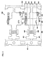
- FIG. 1 is an assembly drawing showing appearances of a card edge connector 500, a substrate 800 and a cable 900 of the embodiment 1 of the present invention.
- the card edge connector 500 includes a housing 700 and a card edge terminal 100.
- the housing 700 is provided with a plurality of through holes 701.
- FIG. 1 Although a single card edge terminal 100 is shown inFIG. 1, it is shown, withothercardedge terminals 100 omitted, for a simplified explanation. A plurality of card edge terminals 100 is actually inserted in the number corresponding to a plurality of through holes 701 of the housing 700.
- the card edge terminal 100 is electrically connected to the cable 900.
- a conductor 902 from which a coated part 901 of the cable 900 is removed is provided at an edge of the cable 900.
- the coated part 901 of the cable 900 and the conductor 902 are attached by crimping the crimping part 400 of the card edge terminal 100.
- the card edge terminal 100 to which the cable 900 is attached by crimping is pressed and inserted into a plurality of through holes 701 on the housing 700.
- Conductor areas 801 are provided on the surface and the back of the substrate 800.
- the conductor areas 801 provided on the surface and the back are electrically conducted via through holes.
- the substrate 800 is inserted and fitted into the housing 700. In this instance, the substrate 800 is held by the holding part 200 (not illustrated) of the card edge terminal 100 pressed and inserted into the housing 700 and electrically conducted to the conductor areas 801.
- the conductor 902 of the cable 900 is electrically conducted to the conductor areas 801 of the substrate 800 via the card edge connector 500.
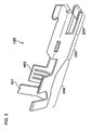
- FIG. 2 is a perspective view showing an appearance of the card edge terminal 100.
- the card edge terminal 100 mainly includes a holding part 200, a box part 300 and a crimping part 400.
- the crimping part 400 includes a first crimping part 401 and a second crimping part 402.
- the first crimping part 401 can prevent a removal of a cable 900 by crimping the coated part 901 of the cable 900.
- the second crimping part 402 electrically connects the card edge terminal 100 with the cable 900 by crimping the conductor 902 of the cable 900.
- the box part 300 has an approximately rectangular cross-section. Further, the holding part 200 formed in communication with the box part 300 is structured so as to retain the substrate 800. The box part 300 and the holding part 200 will be explained later for a detailed configuration.
- the card edge terminal 100 shown in FIG. 2 is formed with a single sheet of an electrically conductive metal member. An explanation will be made for a development view of the card edge terminal 100 and then for the manufacturing process.
- FIG. 3 is a development view of the card edge terminal 100 shown in FIG. 2. As shown in FIG. 3, the card edge terminal 100 is formed by stamping out a single sheet of a metal member.
- apluralityof cardedgeterminals 100 are stamped out from a sheet of a metal member by press working (first process) in a state retained by joint members 450 and 451.
- a plurality of the thus stamped card edge terminals 100 include a part which forms a holding part 200, a box part 300 and a crimping part 400.
- metal plate members corresponding to the card edge terminal 100 , the holding part 200 and the box part 300 shown in FIG. 3 by dividing them into five pieces, namely, a first face 210, a second face 220, a third face 230, a fourth face 240 and a fifth face 250.
- These faces of five-divided pieces are equivalent to faces forming the box part 300 having a rectangular cross section on the card edge terminal 100 to be explained later.
- a rigidity improved part 211, a contact forming part 212, a locking part 213 and a curved part 215 are formed on the first face 210 at the same time by the press working (first process).
- the rigidity improved part 211, the contact forming part 212, the locking part 213 and the curved part 215 on the first face 210 will be explained later for a detailed configuration.
- a rectangular hole 241 is formed on the fourth face 240 at the same time by the press working (first process) .
- a through hole 251 is formed on the fifth face 250 at the same time by the press working (first process).
- the crimping part 400 shown in FIG. 3 is provided with the first crimping part 401 and the second crimping part 402. As explained above, the first crimping part 401 is formed so that the coated part 901 of the cable 900 can be attached by crimping, and the second crimping part 402 is formed so that the conductor 902 of the cable 900 can be attached by crimping.
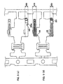
- FIG. 4 through FIG. 7 is flow sheets showing one example of the manufacturing process of the card edge terminal 100. Items from (a) to (g) in FIG. 4 through FIG. 7 show manufacturing processes covering bending or cutting of the card edge terminal 100.
- a collision prevention part 252 which is an area of the fifth face 250 of the card edge terminal 100 is bent toward the direction shown by the arrow x 1 in the drawing.
- a reverse insertion preventing part 253 which is an area of the fifth face 250 of the card edge terminal 100 is bent toward the direction shown by the arrow x 2 in the drawing.
- the reverse insertion preventing part 253 is provided with a foreign matter prevention part 253b.
- a strength supporting part 253a which is another area of the bent reverse insertion preventingpart 253 of the fifth face 250 of the card edge terminal 100 is bent toward the direction shown by the arrow x 3 in the drawing. Since the reverse insertion preventing part 253 is not in a single sheet configuration due to bending of the strength supporting part 253a, strength of the reverse insertion preventing part 253 is improved. Further, the reverse insertion preventing part 253 and the strength supporting part 253a can prevent the removal from the housing 700.
- a whole part of the first face 210 of the card edge terminal 100 is bent toward the direction shown by the arrow x 4 in the drawing, and a whole part of the fifth face is bent toward the direction shown by the arrow x 5 in the drawing.
- an area 242 of the fourth face 240 of the card edge terminal 100 is stamped out.
- the supporting part 231 which is an area of the third face 230 of the card edge terminal 100 is cut away from a joint member 450 and bent toward the direction shown by the arrow x 6.
- the second face 220 and the fourth face 240 are bent respectively toward the directions shown by the arrow x 7 and the arrow x 8.
- the first crimping part 401 and the second crimping part 402 of the crimping part 400 are bent respectively toward the directions shown by the arrow x 9 and the arrow x 10.
- the card edge terminal 100 shown in FIG. 2 is formed in a state connected to the joint member 451.
- the card edge terminal 100 is formed from a single sheet of a metal member through the above-described processes.
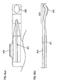
- FIG. 8 is a diagrammatic external view showing the details of the first face 210. (a) shows a plain view of the first face 210, and (b) shows a side view of the first face 210.
- anapproximatelyoval-shaped contact forming part 212 and a curved part 215 are formed at an edge part of the first face 210 by press working (first process).
- a whole part of the edge part of the first face 210 at the curved part 215 is once curved downward and formed so that the edge part of the first face 210 can point upward.
- the curved part 215 is provided with a spring structure due to this configuration.
- a contact forming part 212 is formed at the lowest part where the edge part of the first face 210 is curved. Since the contact forming part 212 is in an approximately oval shape, it is not available in a configuration where one point projects outward but in a configuration where a certain area projects outward. Therefore, an electric contact with conductor areas 801 of the substrate 800 to be explained later is available not at a point but on an area. As a result, the electric conduction with the conductor areas 801 can be attained without fail.
- a rigidity improved part 211 is also formed by press working (firstprocess) at the centerof the first face 210.
- the rigidity improved part 211 is formed linearly in a concave form, thereby improving the rigidity of the first face 210.
- the rigidity improved part 211 acts as a fixed end for the spring structure of the curved part 215.
- a locking part 213 is formed at one end part of the first face 210. Next, an explanation will be made for the function of the locking part 213.
- FIG. 9 is a view for explaining the function of the locking part 213 of the first face 210
- FIG. 10 is a diagrammatic cross-sectional view showing a state that the locking part 213 of first face 210 is fitted into the rectangular hole 241.
- FIG. 10(a) shows the diagrammatic cross section of the box part 300
- FIG. 10 (b) shows the diagrammatic cross section of the holding part 200.
- the locking part 213 of the first face 210 is formed in a tapered shape so that it can be inserted and fitted into the rectangular hole 241.
- the locking part 213 of the first face 210 is inserted and fitted into the rectangular hole 241 formed between the fourth face 240 and the fifth face 250.
- the first face 210 is superimposed vertically on the fifth face 250, and the locking part 213 of the first face 210 is retained by the rectangular hole 241. Further, an approximately rectangular shape is formed by the first face 210, the second face 220, the third face 230 and the fourth face 240 on a box part 300.
- This box part 300 is provided with a rectangular cross section which is strong and free of any clearance, since the first face 210 and the fourth face 240 are fitted to each other by the locking part 213 and the rectangular hole 241.
- a rib configuration 220a is formed at a part of the second face 220 adjacent to the first face 210 in the holding part 200 as well, a supporting-part retaining rib 220b is formed at a part of the second face 220 adjacent to third face 230, a supporting-part retaining rib 240a is formed at a part of the fourth face 240 adjacent to the third face, and a first spring contact part protection rib 240b is formed at a part of the fourth face 240 adjacent to the first face 210.
- the cross section of the holding part 200 is approximately rectangular, strength of the holding part 200 can be improved.
- the first spring contact part protection rib 240b is formed so as to protect the first face 210, there is no direct force applied outside to the spring structure of the curved part 215 on the first face 210. Therefore, the curved part 215 is not deformed and an energizing force from the spring structure can be kept. Further, an energizing force at the curved part 215 of the first face 210 can be supported assuredly by the rigidity improved part 211, the locking part 213 and the rectangular hole 241 on the first face 210.
- FIG. 11 is a diagrammatic perspective view showing a state that a substrate 800 is inserted and fitted into a holding part 200 of a card edge terminal 100.
- the perspective view of the card edge terminal 100 shown in FIG. 11 is described, at an upside down position for a simplified explanation, as compared with the drawing shown in FIG. 1.
- the substrate 800 is inserted and fitted into the holding part 200 of the card edge terminal 100 in the direction shown by the arrow x 20.
- the curved part 215 is protected by the collision prevention part 252 of the fifth face 250 so that an edge of the substrate 800 does not collide directly with the curved part 215 of the first face 210.
- the spring-structured curved part 215 of the first face 210 is externally wrapped by the fifth face 250. Therefore, the substrate 800 will not directly collide with the curved part 215 or deform the curved part 215.
- the substrate 800 is held between the supporting part 231 of the third face 230 and the curved part 215 of the first face 210. Further, the supporting part 231 is a fixed member and supports the substrate 800 when an energizing force is worked from the curved part 215 which presses the substrate 800 to the supporting part 231.
- the supporting part 231 is a fixing member.
- the present invention shall not be restricted thereto and may include any other appropriate fixed members.
- it may be structured so that a spring structure is given to the supporting member 231.
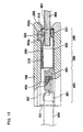
- FIG. 12 is a diagrammatic cross-sectional view showing a state that the cable 900 is attached by crimping to the card edge terminal 100 and inserted into the housing 700 and a substrate 800 is also fitted.
- a coated part 901 is attached by crimping the first crimping part 401 of the crimping part 400 at the card edge terminal 100, and a conductor 902 is attached by crimping the second crimping part.
- the card edge terminal100 to which the cable 900 attached by crimping is inserted and fitted into a through hole 701 of the housing 700.
- anedgeof a reverse insertion preventing part 253 of the fifth face 250 is pressed and inserted into the housing 700.
- the reverse insertion preventing part 253 prevents a reverse insertion of the card edge terminal 100 and the housing 700, thereby fixing the card edge terminal 100 with the housing 700.
- the substrate 800 is inserted and fitted into the holding part 200 of the housing 700.
- the substrate 800 is held between the curved part 215 of the first face 210 and the supporting part 231 of the third face 230 at the holding part 200 retained by the box part 300. Further, as described above, a direct collision of the curved part 215 with an edge of the substrate 800 can be prevented by a collision prevention part 252.
- the holding part 200 can be supported by the box part 300 having an approximately rectangular cross section, it is possible to improve the strength of the holding part 200. Further, since the locking part 213 of the first face 210 at the box part 300 is engaged with rectangular holes 241 on the fourth face 240 and the fifth face 250, the approximately rectangular cross section formed by the first face 210 through the fourth face 240 can be made strong.
- the third face 230 is also supported by supporting-part retaining ribs 220b and 240a provided on the second face 220 and the fourth face 240. As a result, the substrate 800 can be retained more assuredly by the holding part 200.
- the card edge terminal 100 is made from a single sheet of a metal member, it is possible to improve the strength of the card edge terminal 100 itself and also the strength of the box part 300 having an approximately rectangular cross section. It is also possible to reduce the manufacturing cost, compared with a case where a plurality of members is used to manufacture the card edge terminal 100.
- An energizing force works on the conductor areas 801 from the curved part 215 of the holding part 200 and the contact forming part 212 and also the holding part 200 is electrically connected with the crimping part 400 via the boxpart 300, thereby making it possible to electrically connect the conductor areas 801 of the substrate 800 with the conductor 902 of the cable 900 without fail.
- the card edge terminal 100 is structured so as to hold the substrate 800 by the holding part 200, thereby making it possible to partially reduce the height of the card edge terminal 100 by taking advantage of the thickness of the substrate 800. Therefore, the card edge connector 500 can be made lower in height and smaller in size.
- the curved part 215 and the contact forming part 212 are formed integrally into the first face 210, and the surface of the first face 210 is superimposed on the back of the fifth face 250.
- the curved part 215 is protected by the first spring contact part protection rib 240b of the fourth face 240, while the contact forming part 212 is protected by the fifth face 250.
- the supporting part 231 is formed integrally into the third face 230 opposing the first face 210, thereby making it possible to prevent the curved part 215 and the contact forming part 212 from being deformed by an external impact and also to impart to the substrate 800 an energizing force of the curved part 215 and of the contact forming part 212 without fail.
- the card edge terminal 100 can hold the substrate 800 by itself and provide an electric conduction, it will not lose the electric conduction and can provide an electrical connection without fail even when the material of the card edge connector 500 is deteriorated by environmental factors such as vibration and heat. As a result, the card edge connector 500 is available, which has high durability, is resistant to weather, heat and vibration.
- the height of the card edge terminal 100 can be reduced by taking advantage of the thickness of the substrate 800, it is possible to make the card edge connector 500 itself smaller in size and lower in height.
- the substrate 800 is equivalent to the substrate
- the cable 900 is equivalent to the electric wiring
- the card edge terminal 100 is equivalent to the connection terminal
- the conductor 902 is equivalent to the conductor part
- the crimping part 400 is equivalent to the crimping part
- the holding part 200 is equivalent to the holding part
- the conductor areas 801 are equivalent to the conductor areas
- the curved part 215 and the contact forming part 212 are equivalent to the spring contact part
- the box part 300 is equivalent to the box part
- the foreign matter prevention part 253b is equivalent to the foreign matter preventionpart
- the collision prevention part 252 is equivalent to the collision avoidance part and the spring contact part protection face
- the first face 210 is equivalent to the first face
- the second face 220 is equivalent to the second face
- the third face 230 is equivalent to the third face
- the fourth face 240 is equivalent to the fourth face
- the fifth face 250 is equivalent to the fifth face
- the rectangular hole 241 is equivalent to the clearance
- the locking part 213 is equivalent to
- the card edge terminal is formed from a single sheet of a metal plate having an electric conduction.
- the present invention shall not be restricted thereto and may include any given metal or metals made by any given number of metals, etc.
Landscapes
- Coupling Device And Connection With Printed Circuit (AREA)
- Connector Housings Or Holding Contact Members (AREA)
Abstract
Description
- The present invention relates to a connection terminal which can electrically connect an electric wiring with conductor areas of a substrate and also relates to a connector equipped therewith.
- There have been so far developed various types of connectors capable of providing an electrical connection depending on use status. A tuning-fork type contact, a bellows type contact, a cantilever-type contact and others have been used inside these connectors as a connection terminal for providing an electrical connection.
- For example, in some connectors for connecting a cable with a substrate, one end of a tuning-fork type contact is used to hold the cable and the other end of the tuning-fork type contact is inserted into a through hole of the substrate, thereby making it possible to electrically connect the cable with the substrate.
- Japanese Published Unexamined Patent Application No. H11-185898 has disclosed a right angle connector in which contacts can be attached by press-fitting into through holes of a substrate without buckling and connected to the substrate more reliably. Japanese Published Unexamined Patent Application No. 2000-113928 has disclosed a connector in which a locator is used to arrange contacts more accurately and simplify positioning, so that the connector can be assembled more effectively and produced at a lower cost. Further, Japanese Published Unexamined Patent Application No. 2001-6771 has disclosed a connector in which connection terminals can be arranged more accurately and flatness can be improved which is necessary for attaching by press-fitting the connection terminals into a substrate.
- However, in these connectors disclosed in the above documents, since connection terminals are placed on a substrate, the connectors are made greater in height when actually mounted on the substrate. Further, the manufacturing cost is increased because of attaching by press-fitting connection terminals into through holes formed on the substrate.
- Further, the connectors disclosed in the above documents can be used for a prolonged period of time in a desirable environment, for example, in a room. However, in an environment which produces vibration, heat, etc., they cannot be used for a prolonged period of time. For example, resin used for retaining a contact (connection terminal) may be deteriorated due to a heat cycle derived from use or vibration, heat and other factors from the environment. For instance, a fixed end of the connection terminal retained by resin is set free and makes an electrical connection unstable.
- An object of the present invention is to provide a connection terminal, which can be made lower in height and can attain an electrical connection without fail even in an environment which produces vibration and heat and also to provide a connector equipped therewith
- (1)
The connection terminal of the present invention is a connection terminal which connects an electric wiring with a substrate, comprising a crimping part which connects the electric wiring by gripping the conductor part of the electric wiring, a holding part which holds the substrate and also electrically connects conductor areas at a spring contact part which energizes the conductor areas provided at an end part of the substrate and a box part having an approximately rectangular cross section which supports the holding part and electrically communicates with the crimping part. - The connection terminal of the present invention includes a crimping part, a holding part and a box part. The conductor part of an electric wiring is attached by crimping the crimping part, conductor areas fixed on an end part of a substrate are energized by a spring contact part of the holding part, thereby providing an electrical connection. Further, the holding part is supported by the box part, and the crimping part is electrically connected with the box part.
- In this instance, since the holding part is supported by the box part having the approximately rectangular cross section, strength of the holding part can be improved and also the substrate can be more assuredly retained by the holding part. Further, since the spring contact part of the holding part energizes the conductor areas, the substrate can be electrically connected with the conductor areas more assuredly.
In addition, the connection terminal is structured so as to hold the substrate by the holding part, thereby making it possible to partially reduce the height of the connection terminal by taking advantage of the thickness of the substrate. As a result, it can be made lower in height and smaller in size. Further, since the holding part is electrically connected with the crimping part via the box part, it is possible to electrically connect the conductor areas of the substrate with the conductor part of the electric wiring without fail. - Further, since the connection terminal is provided with the holding part and the box part, the fixed end of the connection terminal is not set free and an electrical connection is not made unstable even if resin for retaining the contact (connection terminal) is deteriorated by heat cycle through use or by vibration, heat and other factors coming from a surrounding environment.
- (2)
The holding part may additionally include a foreign matter prevention part which prevents foreign matter from entering into the spring contact part. - In this instance, foreign matter can be prevented from entering into an elastic part of the spring contact part at the holding part, thereby making it possible to stably impart a predetermined energizing force to the conductor areas of the substrate. As a result, it is possible to electrically connect the conductor areas of the substrate without fail.
- (3)
The holding part may additionally include a collision avoidance part which prevents collision of the spring contact part with an end part of the substrate when the substrate is inserted and fitted. - In this instance, collision of the spring contact part with the substrate can be prevented when the substrate is inserted and fitted, thereby making it possible to prevent deformation of the spring contact part. It is, therefore, possible to stably impart a predetermined energizing force to the conductor areas of the substrate. Further, it is possible to prevent deformation of the spring contact part, even when the substrate varies in thickness. As a result, the conductor areas of the substrate can be electrically connected more assuredly.
- (4)
The box part having an approximately rectangular cross section includes in sequence a first face, a second face, a third face, a fourth face and a fifth face which are made by bending a plane member, wherein the back of the fifth face is superimposed on the surface of the first face, an end part of the first face is engaged with a clearance formed between the bent part of the fourth face and that of the fifth face, the spring contact part of the holding part is formed integrally with the first face, and the supporting part is formed integrally on the third face opposing the first face. - In this instance, since an end part of the first face is engaged with a clearance between the fourth face and the fifth face, the approximately rectangular cross section can be made strong by formations of the first face through the fourth face. Further, since the spring contact part is formed integrally on the first face and the surface of the first face is superimposed on the back of the fifth face, it is possible to protect the spring contact part by the fifth face and also prevent deformation of the spring contact part by an external impact. Since the supporting part which supports a substrate is formed integrally on the third face opposing the first face, it is possible to impart an energizing force of the spring contact part to the substrate without fail. As a result, the substrate can be secured to electrically conduct to an electric wiring via the connection terminal.
- (5)
The second face and the fourth face may communicate with the third face and include a supporting-part retaining rib for retaining a supporting part formed on the third face, the fourth face may communicate with the fifth face to retain the fifth face and include a first spring contact part protection rib for protecting the spring contact part of the first face, and the fifth face may include a second spring contact part protection rib for protecting the spring contact part formed on the first face. - In this instance, the supporting part formed on the third face is retained by the supporting-part retaining rib fixed on the second face and the fourth face. Further, the spring contact part is protected by the first spring contact part protection rib provided on the fourth face and the second spring contact part protection rib provided on the fifth face. As a result, the strength of the supporting part can be improved and the spring contact part can be protected, thereby making it possible to impart an energizing force of the spring contact part to the substrate more assuredly.
- (6)
The fifth face may include a spring contact part protection face for protecting the spring contact part by partially bending the fifth face. - In this instance, the spring contact part is protected by the spring contact part protection face. As a result, strength of the supporting part is improved and the spring contact part is protected, thereby making it possible to impart an energizing force of the spring contact part to the substrate more assuredly.
- (7)
The connection terminal may be formed by bending a sheet of a member. The thus formed connection terminal is less likely to vary in dimension of members or produce a clearance than in a case where it is formed with a plurality of members, thereby making it possible to improve the strength of the connection terminal itself and consequently improve the strength of the approximately rectangular cross section of the box part. Therefore, strength of the holding part can be kept high. - In addition, since the connection terminal is constituted with a sheet of a member, it is possible to reduce the manufacturing cost as compared with a case where a plurality of members are used to manufacture connection terminals.
- (8)
Such a connector may be acceptable in which a connection terminal according to any one of Claims 1 to 7 is retained in a housing. - In this instance, since the connection terminal can retain the substrate by itself and provide an electric conduction, the electric conduction can be secured even when a material of the connector is deteriorated in an environment whichproduces vibration, heat, etc. As a result, a connector is available which has durability, is resistant toweather, heat and vibration. Further, since a connection terminal is used to hold a substrate, the height of the connector can be reduced by taking advantage of the thickness of the substrate, thereby making it possible to make the connector smaller in size and lower in height.
-
- FIG. 1 is an assembly view showing appearances of the card edge connector, the electric wiring and the substrate related to the embodiment 1 of the present invention.
- FIG. 2 is a perspective view showing an appearance of the card edge terminal.
- FIG. 3 is a development view of the card edge terminal of FIG. 2.
- FIG. 4 is a flow sheet showing one example of the manufacturing process of the card edge terminal.
- FIG. 5 is a flow sheet showing one example of the manufacturing process of the card edge terminal.
- FIG. 6 is a flow sheet showing one example of the manufacturing process of the card edge terminal.
- FIG. 7 is a flow sheet showing one example of the manufacturing process of the card edge terminal.
- FIG. 8 is a diagrammatic appearance view showing the details of the first face.
- FIG. 9 is a view explaining the action of the first face having a rib configuration.
- FIG. 10 is a diagrammatic cross-sectional view showing a state that the first face having a rib configuration is fitted into a rectangular-shaped hole.
- FIG. 11 is a diagrammatic perspective view showing a state that the substrate is inserted and fitted into the holding part of the card edge terminal.
- FIG. 12 is a diagrammatic cross-sectional view showing a state that the cable is attached by crimping to the card edge terminal and inserted into the housing and the substrate is also fitted thereinto.
- Hereinafter, an explanation will be made for embodiments of the present invention. In these embodiments, an explanation will be made for a case where a card edge connector is used as an example of connectors, and an explanation will be made for a case where a card edge terminal inserted and fitted into a card edge connector is used as a connection terminal.
- (Embodiment 1)
FIG. 1 is an assembly drawing showing appearances of acard edge connector 500, asubstrate 800 and acable 900 of the embodiment 1 of the present invention.
As shown in FIG. 1, thecard edge connector 500 includes ahousing 700 and acard edge terminal 100. Thehousing 700 is provided with a plurality of throughholes 701. - Further, although a single
card edge terminal 100 is shown inFIG. 1, it is shown,withothercardedge terminals 100 omitted, for a simplified explanation. A plurality ofcard edge terminals 100 is actually inserted in the number corresponding to a plurality of throughholes 701 of thehousing 700. - The
card edge terminal 100 is electrically connected to thecable 900. Aconductor 902 from which acoated part 901 of thecable 900 is removed is provided at an edge of thecable 900. As will be explained later, thecoated part 901 of thecable 900 and theconductor 902 are attached by crimping the crimpingpart 400 of thecard edge terminal 100. Thecard edge terminal 100 to which thecable 900 is attached by crimping is pressed and inserted into a plurality of throughholes 701 on thehousing 700. -
Conductor areas 801 are provided on the surface and the back of thesubstrate 800. Theconductor areas 801 provided on the surface and the back are electrically conducted via through holes. Thesubstrate 800 is inserted and fitted into thehousing 700. In this instance, thesubstrate 800 is held by the holding part 200 (not illustrated) of thecard edge terminal 100 pressed and inserted into thehousing 700 and electrically conducted to theconductor areas 801. - As a result, the
conductor 902 of thecable 900 is electrically conducted to theconductor areas 801 of thesubstrate 800 via thecard edge connector 500. - FIG. 2 is a perspective view showing an appearance of the
card edge terminal 100.
As shown in FIG. 2, thecard edge terminal 100 mainly includes a holdingpart 200, abox part 300 and a crimpingpart 400. - The crimping
part 400 includes a first crimpingpart 401 and a second crimpingpart 402. The first crimpingpart 401 can prevent a removal of acable 900 by crimping thecoated part 901 of thecable 900. The second crimpingpart 402 electrically connects thecard edge terminal 100 with thecable 900 by crimping theconductor 902 of thecable 900. - Next, the
box part 300 has an approximately rectangular cross-section. Further, the holdingpart 200 formed in communication with thebox part 300 is structured so as to retain thesubstrate 800. Thebox part 300 and the holdingpart 200 will be explained later for a detailed configuration. - The
card edge terminal 100 shown in FIG. 2 is formed with a single sheet of an electrically conductive metal member. An explanation will be made for a development view of thecard edge terminal 100 and then for the manufacturing process. - FIG. 3 is a development view of the
card edge terminal 100 shown in FIG. 2.
As shown in FIG. 3, thecard edge terminal 100 is formed by stamping out a single sheet of a metal member. - First, asshowninFIG. 3, apluralityof cardedgeterminals 100 are stamped out from a sheet of a metal member by press working (first process) in a state retained by
joint members - A plurality of the thus stamped
card edge terminals 100 include a part which forms a holdingpart 200, abox part 300 and a crimpingpart 400. - Hereinafter, an explanation will be made for metal plate members corresponding to the
card edge terminal 100 , the holdingpart 200 and thebox part 300 shown in FIG. 3 by dividing them into five pieces, namely, afirst face 210, asecond face 220, athird face 230, afourth face 240 and afifth face 250. These faces of five-divided pieces are equivalent to faces forming thebox part 300 having a rectangular cross section on thecard edge terminal 100 to be explained later. - Further, as shown in FIG. 3, a rigidity
improved part 211, acontact forming part 212, a lockingpart 213 and a curved part 215 (not illustrated) are formed on thefirst face 210 at the same time by the press working (first process). The rigidity improvedpart 211, thecontact forming part 212, the lockingpart 213 and thecurved part 215 on thefirst face 210 will be explained later for a detailed configuration. - Further, a
rectangular hole 241 is formed on thefourth face 240 at the same time by the press working (first process) .
Next, a throughhole 251 is formed on thefifth face 250 at the same time by the press working (first process). - The crimping
part 400 shown in FIG. 3 is provided with the first crimpingpart 401 and the second crimpingpart 402.
As explained above, the first crimpingpart 401 is formed so that thecoated part 901 of thecable 900 can be attached by crimping, and the second crimpingpart 402 is formed so that theconductor 902 of thecable 900 can be attached by crimping. - Next, an explanation will be made for the manufacturing process of the
card edge terminal 100 shown in FIG. 3 by referring to FIG. 4 through FIG. 7. - FIG. 4 through FIG. 7 is flow sheets showing one example of the manufacturing process of the
card edge terminal 100. Items from (a) to (g) in FIG. 4 through FIG. 7 show manufacturing processes covering bending or cutting of thecard edge terminal 100. - At first, as shown in FIG. 4 (a), a
collision prevention part 252, which is an area of thefifth face 250 of thecard edge terminal 100 is bent toward the direction shown by the arrow x 1 in the drawing. - Next, as shown in FIG. 4(b), a reverse
insertion preventing part 253 which is an area of thefifth face 250 of thecard edge terminal 100 is bent toward the direction shown by the arrow x 2 in the drawing. - In this instance, since the through
hole 251 is stamped out so as to partially form a protrusion in place of a rectangular form, the reverseinsertion preventing part 253 is provided with a foreignmatter prevention part 253b. - Next, as shown in FIG. 5 (c), a
strength supporting part 253a which is another area of the bentreverse insertion preventingpart 253 of thefifth face 250 of thecard edge terminal 100 is bent toward the direction shown by the arrow x 3 in the drawing. Since the reverseinsertion preventing part 253 is not in a single sheet configuration due to bending of thestrength supporting part 253a, strength of the reverseinsertion preventing part 253 is improved. Further, the reverseinsertion preventing part 253 and thestrength supporting part 253a can prevent the removal from thehousing 700. - Next, as shown in FIG. 5(d), a whole part of the
first face 210 of thecard edge terminal 100 is bent toward the direction shown by the arrow x 4 in the drawing, and a whole part of the fifth face is bent toward the direction shown by the arrow x 5 in the drawing. - Next, as shown in FIG. 6(e), an
area 242 of thefourth face 240 of thecard edge terminal 100 is stamped out. - Next, as shown in FIG. 6 (f), the supporting
part 231 which is an area of thethird face 230 of thecard edge terminal 100 is cut away from ajoint member 450 and bent toward the direction shown by the arrow x 6. Thereafter, thesecond face 220 and thefourth face 240 are bent respectively toward the directions shown by the arrow x 7 and the arrow x 8. The first crimpingpart 401 and the second crimpingpart 402 of the crimpingpart 400 are bent respectively toward the directions shown by the arrow x 9 and the arrow x 10. - Finally, as shown in FIG. 7(g), the
card edge terminal 100 shown in FIG. 2 is formed in a state connected to thejoint member 451. - The
card edge terminal 100 is formed from a single sheet of a metal member through the above-described processes. - Next, an explanation will be made regarding the details of the
first face 210. FIG. 8 is a diagrammatic external view showing the details of thefirst face 210. (a) shows a plain view of thefirst face 210, and (b) shows a side view of thefirst face 210. - As shown in FIG. 8(a) and (b), anapproximatelyoval-shaped
contact forming part 212 and acurved part 215 are formed at an edge part of thefirst face 210 by press working (first process). - As shown in FIG. 8 (b), a whole part of the edge part of the
first face 210 at thecurved part 215 is once curved downward and formed so that the edge part of thefirst face 210 can point upward. Thecurved part 215 is provided with a spring structure due to this configuration. - In addition, a
contact forming part 212 is formed at the lowest part where the edge part of thefirst face 210 is curved.
Since thecontact forming part 212 is in an approximately oval shape, it is not available in a configuration where one point projects outward but in a configuration where a certain area projects outward. Therefore, an electric contact withconductor areas 801 of thesubstrate 800 to be explained later is available not at a point but on an area. As a result, the electric conduction with theconductor areas 801 can be attained without fail. - A rigidity improved
part 211 is also formed by press working (firstprocess) at the centerof thefirst face 210. The rigidity improvedpart 211 is formed linearly in a concave form, thereby improving the rigidity of thefirst face 210. The rigidity improvedpart 211 acts as a fixed end for the spring structure of thecurved part 215. - A locking
part 213 is formed at one end part of thefirst face 210. Next, an explanation will be made for the function of the lockingpart 213. - FIG. 9 is a view for explaining the function of the locking
part 213 of thefirst face 210, and FIG. 10 is a diagrammatic cross-sectional view showing a state that the lockingpart 213 offirst face 210 is fitted into therectangular hole 241. Further, FIG. 10(a) shows the diagrammatic cross section of thebox part 300, and FIG. 10 (b) shows the diagrammatic cross section of the holdingpart 200. - As shown in FIG. 9, the locking
part 213 of thefirst face 210 is formed in a tapered shape so that it can be inserted and fitted into therectangular hole 241. In the above-described process in FIG. 6 (f), the lockingpart 213 of thefirst face 210 is inserted and fitted into therectangular hole 241 formed between thefourth face 240 and thefifth face 250. - As a result, as shown in FIG. 10(a), the
first face 210 is superimposed vertically on thefifth face 250, and the lockingpart 213 of thefirst face 210 is retained by therectangular hole 241. Further, an approximately rectangular shape is formed by thefirst face 210, thesecond face 220, thethird face 230 and thefourth face 240 on abox part 300. - This
box part 300 is provided with a rectangular cross section which is strong and free of any clearance, since thefirst face 210 and thefourth face 240 are fitted to each other by the lockingpart 213 and therectangular hole 241. - As shown in FIG. 10 (b), a
rib configuration 220a is formed at a part of thesecond face 220 adjacent to thefirst face 210 in the holdingpart 200 as well, a supporting-part retaining rib 220b is formed at a part of thesecond face 220 adjacent tothird face 230, a supporting-part retaining rib 240a is formed at a part of thefourth face 240 adjacent to the third face, and a first spring contactpart protection rib 240b is formed at a part of thefourth face 240 adjacent to thefirst face 210. In this instance, since the cross section of the holdingpart 200 is approximately rectangular, strength of the holdingpart 200 can be improved. - Further, since the first spring contact
part protection rib 240b is formed so as to protect thefirst face 210, there is no direct force applied outside to the spring structure of thecurved part 215 on thefirst face 210. Therefore, thecurved part 215 is not deformed and an energizing force from the spring structure can be kept. Further, an energizing force at thecurved part 215 of thefirst face 210 can be supported assuredly by the rigidity improvedpart 211, the lockingpart 213 and therectangular hole 241 on thefirst face 210. - Next, FIG. 11 is a diagrammatic perspective view showing a state that a
substrate 800 is inserted and fitted into a holdingpart 200 of acard edge terminal 100. The perspective view of thecard edge terminal 100 shown in FIG. 11 is described, at an upside down position for a simplified explanation, as compared with the drawing shown in FIG. 1. - As shown in FIG. 11, at first, the
substrate 800 is inserted and fitted into the holdingpart 200 of thecard edge terminal 100 in the direction shown by the arrow x 20. In this instance, thecurved part 215 is protected by thecollision prevention part 252 of thefifth face 250 so that an edge of thesubstrate 800 does not collide directly with thecurved part 215 of thefirst face 210. - Further, the spring-structured
curved part 215 of thefirst face 210 is externally wrapped by thefifth face 250. Therefore, thesubstrate 800 will not directly collide with thecurved part 215 or deform thecurved part 215. - The
substrate 800 is held between the supportingpart 231 of thethird face 230 and thecurved part 215 of thefirst face 210. Further, the supportingpart 231 is a fixed member and supports thesubstrate 800 when an energizing force is worked from thecurved part 215 which presses thesubstrate 800 to the supportingpart 231. - In the present embodiment, the supporting
part 231 is a fixing member. However, the present invention shall not be restricted thereto and may include any other appropriate fixed members. For example, it may be structured so that a spring structure is given to the supportingmember 231. - FIG. 12 is a diagrammatic cross-sectional view showing a state that the
cable 900 is attached by crimping to thecard edge terminal 100 and inserted into thehousing 700 and asubstrate 800 is also fitted. - As shown in FIG. 12, a
coated part 901 is attached by crimping the first crimpingpart 401 of the crimpingpart 400 at thecard edge terminal 100, and aconductor 902 is attached by crimping the second crimping part. - The card edge terminal100 to which the
cable 900 attached by crimping is inserted and fitted into a throughhole 701 of thehousing 700. In this instance, anedgeof a reverseinsertion preventing part 253 of thefifth face 250 is pressed and inserted into thehousing 700. The reverseinsertion preventing part 253 prevents a reverse insertion of thecard edge terminal 100 and thehousing 700, thereby fixing thecard edge terminal 100 with thehousing 700. - Next, the
substrate 800 is inserted and fitted into the holdingpart 200 of thehousing 700. Thesubstrate 800 is held between thecurved part 215 of thefirst face 210 and the supportingpart 231 of thethird face 230 at the holdingpart 200 retained by thebox part 300. Further, as described above, a direct collision of thecurved part 215 with an edge of thesubstrate 800 can be prevented by acollision prevention part 252. - Entrance of foreign matter into a space below the
curved part 215 can be prevented by the foreignmatter prevention part 253b of the reverseinsertion preventing part 253 on thefifth face 250, thereby making it possible to secure the space so that thecurved part 215 can be bent downward. In this instance, since an energizing force of thecurved part 215 is protected, it is possible to stably impart a predetermined energizing force to theconductor areas 801 of thesubstrate 800 from the supportingpart 231 and thecurved part 215. As a result, theconductor areas 801 of thesubstrate 800 can be electrically connected without fail. - Therefore, in the
card edge terminal 100 of the present invention, since the holdingpart 200 can be supported by thebox part 300 having an approximately rectangular cross section, it is possible to improve the strength of the holdingpart 200.
Further, since the lockingpart 213 of thefirst face 210 at thebox part 300 is engaged withrectangular holes 241 on thefourth face 240 and thefifth face 250, the approximately rectangular cross section formed by thefirst face 210 through thefourth face 240 can be made strong. Thethird face 230 is also supported by supporting-part retaining ribs second face 220 and thefourth face 240. As a result, thesubstrate 800 can be retained more assuredly by the holdingpart 200. - Further, since the
card edge terminal 100 is made from a single sheet of a metal member, it is possible to improve the strength of thecard edge terminal 100 itself and also the strength of thebox part 300 having an approximately rectangular cross section. It is also possible to reduce the manufacturing cost, compared with a case where a plurality of members is used to manufacture thecard edge terminal 100. - An energizing force works on the
conductor areas 801 from thecurved part 215 of the holdingpart 200 and thecontact forming part 212 and also the holdingpart 200 is electrically connected with the crimpingpart 400 via theboxpart 300, thereby making it possible to electrically connect theconductor areas 801 of thesubstrate 800 with theconductor 902 of thecable 900 without fail. - Further, the
card edge terminal 100 is structured so as to hold thesubstrate 800 by the holdingpart 200, thereby making it possible to partially reduce the height of thecard edge terminal 100 by taking advantage of the thickness of thesubstrate 800. Therefore, thecard edge connector 500 can be made lower in height and smaller in size. - In addition, the
curved part 215 and thecontact forming part 212 are formed integrally into thefirst face 210, and the surface of thefirst face 210 is superimposed on the back of thefifth face 250. Thecurved part 215 is protected by the first spring contactpart protection rib 240b of thefourth face 240, while thecontact forming part 212 is protected by thefifth face 250. Further, the supportingpart 231 is formed integrally into thethird face 230 opposing thefirst face 210, thereby making it possible to prevent thecurved part 215 and thecontact forming part 212 from being deformed by an external impact and also to impart to thesubstrate 800 an energizing force of thecurved part 215 and of thecontact forming part 212 without fail. - Further, since the
card edge terminal 100 can hold thesubstrate 800 by itself and provide an electric conduction, it will not lose the electric conduction and can provide an electrical connection without fail even when the material of thecard edge connector 500 is deteriorated by environmental factors such as vibration and heat. As a result, thecard edge connector 500 is available, which has high durability, is resistant to weather, heat and vibration. - Further, since the height of the
card edge terminal 100 can be reduced by taking advantage of the thickness of thesubstrate 800, it is possible to make thecard edge connector 500 itself smaller in size and lower in height. - In the above-described embodiment 1, the substrate 800 is equivalent to the substrate, the cable 900 is equivalent to the electric wiring, the card edge terminal 100 is equivalent to the connection terminal, the conductor 902 is equivalent to the conductor part, the crimping part 400 is equivalent to the crimping part, the holding part 200 is equivalent to the holding part, the conductor areas 801 are equivalent to the conductor areas, the curved part 215 and the contact forming part 212 are equivalent to the spring contact part, the box part 300 is equivalent to the box part, the foreign matter prevention part 253b is equivalent to the foreign matter preventionpart, the collision prevention part 252 is equivalent to the collision avoidance part and the spring contact part protection face, the first face 210 is equivalent to the first face, the second face 220 is equivalent to the second face, the third face 230 is equivalent to the third face, the fourth face 240 is equivalent to the fourth face, the fifth face 250 is equivalent to the fifth face, the rectangular hole 241 is equivalent to the clearance, the locking part 213 is equivalent to an end part of the first face, the supporting part 231 is equivalent to the supporting part, the supporting-part retaining rib 220b and the supporting-part retaining rib 240a are equivalent to the supporting-part retaining ribs, the first spring contact part protection rib 240b is equivalent to the first spring contact part protection rib, the reverse insertion preventing part 253 is equivalent to the second spring contact part protection rib, and the housing 700 is equivalent to the housing.
- Further, the card edge terminal is formed from a single sheet of a metal plate having an electric conduction. However, the present invention shall not be restricted thereto and may include any given metal or metals made by any given number of metals, etc.
- The present invention has been described in the above-described preferable embodiment. However, the present invention shall not be restricted thereto alone and it is apparent that the present invention may be applicable to any other embodiments, without deviating from the spirit and scope of the present invention. Further, the present embodiment has described the actions and effects when constituted according to the present invention. However, these actions and effects are only one example and shall not be construed to restrict the present invention.
Claims (8)
- A connection terminal which connects a substrate (800) with an electric wiring, characterized in that it comprises a crimping part (400) for connecting the electric wiring (900) by griping a conductor part (902) of the electric wiring, a holdingpart (200) which holds the substrate between a supporting part (231) and a spring contact part (215) that energizes the conductor areas fixed at an end part of the substrate and also electrically connects the conductor areas (801), and a box part (300) having an approximately rectangular cross section which supports the holding part and also electrically connects the crimping part.
- A connection terminal according to Claim 1, characterized in that the holding part (200) additionally includes a foreign matter prevention part (253b) for preventing foreign matter from entering into the spring contact part (215) .
- A connection terminal according to Claim 1 or 2, characterized in that the holding part (200) additionally includes a collision avoidance part (252) for preventing collision of the spring contact part (215) with an end part of the substrate (800) when the substrate is inserted and fitted.
- A connection terminal according to anyone of Claims 1 to 3, characterized in that an approximately rectangular cross section of the box part (300) includes in sequence a first face (210), a second face (220), a third face (230), a fourth face (240) and a fifth face (250) which are made by bending a plane member, the back of the fifth face is superimposed on the surface of the first face, an end part of the first face (213) is engaged with a clearance (241) formed between the bent part of the fourth face and that of the fifth face, the spring contact part (215) of the holding part is formed integrally with the first face, and the supporting part is formed integrally on the third face opposing the first face.
- A connection terminal according to Claim 4, characterized in that the second face (220) and the fourth face (240) communicate with the third face (230) and include a supporting-part retaining rib (220b, 240a) for retaining a supporting part formed on the third face, the fourth face communicates with the fifth face (250) to retain the fifth face and includes a first spring contact part protection rib (240b) for protecting the spring contact part of the first face, and the fifth face includes a second spring contact part protection rib (253) for protecting the spring contact part (215) formed on the first face.
- A connection terminal according to Claim 4 or 5 characterized in that the fifth face includes a spring contact part protection face (252) for protecting the spring contact part by partially bending the fifth face.
- A connection terminal according to any one of Claims 1 to 6 characterized in that the connection terminal is formed by bending a single sheet of a plane member.
- A connector characterized in that it comprises a connection terminal according to any one of Claims 1 to 7 and a housing (700) which retains the connection terminal.
Applications Claiming Priority (1)
| Application Number | Priority Date | Filing Date | Title |
|---|---|---|---|
| JP2004372565A JP2006179362A (en) | 2004-12-24 | 2004-12-24 | Connection terminal and connector equipped with the same |
Publications (2)
| Publication Number | Publication Date |
|---|---|
| EP1675222A1 true EP1675222A1 (en) | 2006-06-28 |
| EP1675222B1 EP1675222B1 (en) | 2007-08-15 |
Family
ID=36199610
Family Applications (1)
| Application Number | Title | Priority Date | Filing Date |
|---|---|---|---|
| EP05292777A Expired - Lifetime EP1675222B1 (en) | 2004-12-24 | 2005-12-23 | Connection terminal and connector equipped therewith |
Country Status (4)
| Country | Link |
|---|---|
| US (1) | US7198525B2 (en) |
| EP (1) | EP1675222B1 (en) |
| JP (1) | JP2006179362A (en) |
| DE (1) | DE602005002016T2 (en) |
Cited By (1)
| Publication number | Priority date | Publication date | Assignee | Title |
|---|---|---|---|---|
| EP2363922A1 (en) * | 2010-03-01 | 2011-09-07 | Sumitomo Wiring Systems, Ltd. | Connector |
Families Citing this family (14)
| Publication number | Priority date | Publication date | Assignee | Title |
|---|---|---|---|---|
| FR2869161B1 (en) * | 2004-04-19 | 2007-04-20 | Fci Sa | ELECTRIC CONTACT, AND ELECTRICAL CONNECTOR PART COMPRISING SUCH CONTACT |
| KR100833602B1 (en) | 2006-09-14 | 2008-05-30 | 한국단자공업 주식회사 | Receptacle Terminal |
| US7402089B1 (en) * | 2007-05-04 | 2008-07-22 | Tyco Electronics Corporation | Contact with enhanced transition region |
| JP5586192B2 (en) * | 2009-09-03 | 2014-09-10 | 矢崎総業株式会社 | Connector terminal |
| JP6342608B2 (en) * | 2012-12-04 | 2018-06-13 | 矢崎総業株式会社 | Female terminal |
| JP6132207B2 (en) * | 2014-03-13 | 2017-05-24 | 住友電装株式会社 | Terminal fittings and connectors |
| JP6609210B2 (en) * | 2016-03-25 | 2019-11-20 | 日本圧着端子製造株式会社 | Connector with locking mechanism |
| KR101780363B1 (en) | 2016-04-18 | 2017-09-26 | (주)우주일렉트로닉스 | Connector for connecting board |
| CN206364484U (en) * | 2016-12-19 | 2017-07-28 | 番禺得意精密电子工业有限公司 | Cable installation |
| KR102106925B1 (en) * | 2018-09-05 | 2020-05-06 | 주식회사 유라 | Connector assembly and connector therefor |
| KR102055392B1 (en) * | 2018-10-08 | 2020-01-22 | 주식회사 유라 | Female terminal |
| JP2021089834A (en) * | 2019-12-04 | 2021-06-10 | 住友電装株式会社 | Terminal fitting |
| CN117727708B (en) * | 2023-12-15 | 2024-05-28 | 宁波君芯半导体有限公司 | Silicon carbide power device and processing method thereof |
| KR102836038B1 (en) * | 2024-12-27 | 2025-07-21 | 주식회사 엠텍 | Electrical connector and terminal of the same |
Citations (7)
| Publication number | Priority date | Publication date | Assignee | Title |
|---|---|---|---|---|
| US5238411A (en) * | 1991-03-28 | 1993-08-24 | Yazaki Corporation | Connector for printed circuit board |
| JPH11185898A (en) | 1997-12-22 | 1999-07-09 | Japan Aviation Electron Ind Ltd | Right angle connector |
| JP2000113928A (en) | 1998-10-05 | 2000-04-21 | Japan Aviation Electronics Industry Ltd | connector |
| WO2000074176A1 (en) * | 1999-05-28 | 2000-12-07 | The Whitaker Corporation | Electrical contact receptacle terminal to mate with round and rectangular pins |
| JP2001006771A (en) | 1999-06-18 | 2001-01-12 | Nec Corp | Connector |
| JP2003331965A (en) * | 2002-05-17 | 2003-11-21 | Ryosei Electro-Circuit Systems Ltd | Connecting terminal |
| US6804122B1 (en) * | 2003-08-12 | 2004-10-12 | Yazaki North America, Inc. | Self-stabilizing card edge terminal |
Family Cites Families (8)
| Publication number | Priority date | Publication date | Assignee | Title |
|---|---|---|---|---|
| JPH0557767U (en) * | 1992-01-06 | 1993-07-30 | 日本航空電子工業株式会社 | contact |
| JP3278017B2 (en) * | 1994-03-31 | 2002-04-30 | タイコエレクトロニクスアンプ株式会社 | Receptacle contact |
| DE19535148A1 (en) * | 1995-09-21 | 1997-03-27 | Whitaker Corp | Part of an electrical contact and electrical contact |
| US5997363A (en) * | 1996-12-18 | 1999-12-07 | The Whitaker Corporation | Single piece electrical terminal for sealed connectors |
| JP3307877B2 (en) * | 1997-05-29 | 2002-07-24 | タイコエレクトロニクスアンプ株式会社 | Electrical contacts |
| JP2003077569A (en) * | 2001-09-03 | 2003-03-14 | Sumitomo Wiring Syst Ltd | Female side terminal fitting |
| JP3993463B2 (en) * | 2002-05-17 | 2007-10-17 | 三菱電線工業株式会社 | Connecting terminal |
| JP2004103347A (en) * | 2002-09-09 | 2004-04-02 | Sumitomo Wiring Syst Ltd | Connector |
-
2004
- 2004-12-24 JP JP2004372565A patent/JP2006179362A/en active Pending
-
2005
- 2005-12-22 US US11/315,450 patent/US7198525B2/en not_active Expired - Lifetime
- 2005-12-23 EP EP05292777A patent/EP1675222B1/en not_active Expired - Lifetime
- 2005-12-23 DE DE602005002016T patent/DE602005002016T2/en not_active Expired - Lifetime
Patent Citations (7)
| Publication number | Priority date | Publication date | Assignee | Title |
|---|---|---|---|---|
| US5238411A (en) * | 1991-03-28 | 1993-08-24 | Yazaki Corporation | Connector for printed circuit board |
| JPH11185898A (en) | 1997-12-22 | 1999-07-09 | Japan Aviation Electron Ind Ltd | Right angle connector |
| JP2000113928A (en) | 1998-10-05 | 2000-04-21 | Japan Aviation Electronics Industry Ltd | connector |
| WO2000074176A1 (en) * | 1999-05-28 | 2000-12-07 | The Whitaker Corporation | Electrical contact receptacle terminal to mate with round and rectangular pins |
| JP2001006771A (en) | 1999-06-18 | 2001-01-12 | Nec Corp | Connector |
| JP2003331965A (en) * | 2002-05-17 | 2003-11-21 | Ryosei Electro-Circuit Systems Ltd | Connecting terminal |
| US6804122B1 (en) * | 2003-08-12 | 2004-10-12 | Yazaki North America, Inc. | Self-stabilizing card edge terminal |
Non-Patent Citations (1)
| Title |
|---|
| PATENT ABSTRACTS OF JAPAN vol. 2003, no. 12 5 December 2003 (2003-12-05) * |
Cited By (1)
| Publication number | Priority date | Publication date | Assignee | Title |
|---|---|---|---|---|
| EP2363922A1 (en) * | 2010-03-01 | 2011-09-07 | Sumitomo Wiring Systems, Ltd. | Connector |
Also Published As
| Publication number | Publication date |
|---|---|
| JP2006179362A (en) | 2006-07-06 |
| US20060138637A1 (en) | 2006-06-29 |
| US7198525B2 (en) | 2007-04-03 |
| EP1675222B1 (en) | 2007-08-15 |
| DE602005002016T2 (en) | 2008-05-08 |
| DE602005002016D1 (en) | 2007-09-27 |
Similar Documents
| Publication | Publication Date | Title |
|---|---|---|
| EP2507871B1 (en) | Electrical terminal | |
| EP1675222B1 (en) | Connection terminal and connector equipped therewith | |
| EP2019456B1 (en) | Electric connector | |
| JP5956071B2 (en) | Connecting terminal | |
| EP1962383A2 (en) | Electrical connector and combination connector having the same | |
| US7275946B2 (en) | Electric connector for wiring harness having a short circuit terminal | |
| US9461385B2 (en) | Card edge connector | |
| JP6933975B2 (en) | Electrical connector for circuit board | |
| JP2005294217A (en) | Pressure contact type contact and electrical connector using the same | |
| US9022817B2 (en) | Connector terminal including limiter extending along first and second spring terminals | |
| KR100567587B1 (en) | Electrical connector having a holddown for ground connection | |
| JP3812937B2 (en) | connector | |
| KR20230095810A (en) | Connector and connector assembly | |
| EP0762551A2 (en) | Electrical terminal with locking lance | |
| JP5650487B2 (en) | connector | |
| JPH06260238A (en) | Connecting terminal | |
| CN104170176B (en) | Connection terminals and connectors using connection terminals | |
| CN110233370A (en) | Terminal, connector and electrical connector | |
| JP7498431B2 (en) | Terminal unit and female terminal used therein | |
| CN214204029U (en) | Connector and conductive shell for connector | |
| JP7543948B2 (en) | Terminal unit and female terminal used in terminal unit | |
| JP4353433B2 (en) | connector | |
| CN114514657B (en) | Connector and connector assembly | |
| JP7655707B2 (en) | connector | |
| JP4274564B2 (en) | Multi-pole connector |
Legal Events
| Date | Code | Title | Description |
|---|---|---|---|
| PUAI | Public reference made under article 153(3) epc to a published international application that has entered the european phase |
Free format text: ORIGINAL CODE: 0009012 |
|
| AK | Designated contracting states |
Kind code of ref document: A1 Designated state(s): AT BE BG CH CY CZ DE DK EE ES FI FR GB GR HU IE IS IT LI LT LU LV MC NL PL PT RO SE SI SK TR |
|
| AX | Request for extension of the european patent |
Extension state: AL BA HR MK YU |
|
| 17P | Request for examination filed |
Effective date: 20061226 |
|
| GRAP | Despatch of communication of intention to grant a patent |
Free format text: ORIGINAL CODE: EPIDOSNIGR1 |
|
| AKX | Designation fees paid |
Designated state(s): DE FR |
|
| RIN1 | Information on inventor provided before grant (corrected) |
Inventor name: NAGAMINE, AKIRAC/O J.S.T. MFG. CO., LTD Inventor name: CHIYODA, MEGUMIC/O J.S.T. MFG. CO., LTD |
|
| GRAS | Grant fee paid |
Free format text: ORIGINAL CODE: EPIDOSNIGR3 |
|
| GRAA | (expected) grant |
Free format text: ORIGINAL CODE: 0009210 |
|
| AK | Designated contracting states |
Kind code of ref document: B1 Designated state(s): DE FR |
|
| REF | Corresponds to: |
Ref document number: 602005002016 Country of ref document: DE Date of ref document: 20070927 Kind code of ref document: P |
|
| ET | Fr: translation filed | ||
| PLBE | No opposition filed within time limit |
Free format text: ORIGINAL CODE: 0009261 |
|
| STAA | Information on the status of an ep patent application or granted ep patent |
Free format text: STATUS: NO OPPOSITION FILED WITHIN TIME LIMIT |
|
| 26N | No opposition filed |
Effective date: 20080516 |
|
| REG | Reference to a national code |
Ref country code: FR Ref legal event code: PLFP Year of fee payment: 11 |
|
| REG | Reference to a national code |
Ref country code: FR Ref legal event code: PLFP Year of fee payment: 12 |
|
| REG | Reference to a national code |
Ref country code: FR Ref legal event code: PLFP Year of fee payment: 13 |
|
| REG | Reference to a national code |
Ref country code: DE Ref legal event code: R082 Ref document number: 602005002016 Country of ref document: DE Representative=s name: CBDL PATENTANWAELTE GBR, DE Ref country code: DE Ref legal event code: R082 Ref document number: 602005002016 Country of ref document: DE Representative=s name: CBDL PATENTANWAELTE EGBR, DE |
|
| PGFP | Annual fee paid to national office [announced via postgrant information from national office to epo] |
Ref country code: DE Payment date: 20241210 Year of fee payment: 20 |
|
| PGFP | Annual fee paid to national office [announced via postgrant information from national office to epo] |
Ref country code: FR Payment date: 20241223 Year of fee payment: 20 |
|
| REG | Reference to a national code |
Ref country code: DE Ref legal event code: R071 Ref document number: 602005002016 Country of ref document: DE |