EP1672907A1 - Pixel interpolation circuit and pixel interpolation method, and image reader - Google Patents
Pixel interpolation circuit and pixel interpolation method, and image reader Download PDFInfo
- Publication number
- EP1672907A1 EP1672907A1 EP04746648A EP04746648A EP1672907A1 EP 1672907 A1 EP1672907 A1 EP 1672907A1 EP 04746648 A EP04746648 A EP 04746648A EP 04746648 A EP04746648 A EP 04746648A EP 1672907 A1 EP1672907 A1 EP 1672907A1
- Authority
- EP
- European Patent Office
- Prior art keywords
- interpolation
- data
- pixel
- test
- circuit
- Prior art date
- Legal status (The legal status is an assumption and is not a legal conclusion. Google has not performed a legal analysis and makes no representation as to the accuracy of the status listed.)
- Withdrawn
Links
Images




Classifications
-
- G—PHYSICS
- G06—COMPUTING OR CALCULATING; COUNTING
- G06T—IMAGE DATA PROCESSING OR GENERATION, IN GENERAL
- G06T3/00—Geometric image transformations in the plane of the image
- G06T3/10—Selection of transformation methods according to the characteristics of the input images
-
- G—PHYSICS
- G06—COMPUTING OR CALCULATING; COUNTING
- G06T—IMAGE DATA PROCESSING OR GENERATION, IN GENERAL
- G06T5/00—Image enhancement or restoration
- G06T5/20—Image enhancement or restoration using local operators
-
- H—ELECTRICITY
- H04—ELECTRIC COMMUNICATION TECHNIQUE
- H04N—PICTORIAL COMMUNICATION, e.g. TELEVISION
- H04N1/00—Scanning, transmission or reproduction of documents or the like, e.g. facsimile transmission; Details thereof
- H04N1/40—Picture signal circuits
- H04N1/401—Compensating positionally unequal response of the pick-up or reproducing head
-
- H—ELECTRICITY
- H04—ELECTRIC COMMUNICATION TECHNIQUE
- H04N—PICTORIAL COMMUNICATION, e.g. TELEVISION
- H04N2209/00—Details of colour television systems
- H04N2209/04—Picture signal generators
- H04N2209/041—Picture signal generators using solid-state devices
- H04N2209/042—Picture signal generators using solid-state devices having a single pick-up sensor
- H04N2209/045—Picture signal generators using solid-state devices having a single pick-up sensor using mosaic colour filter
- H04N2209/046—Colour interpolation to calculate the missing colour values
Definitions
- This invention is related to an image processing method applied to an image scanner using an image sensor, and particularly to a method of generating interpolation pixel data for a digital image.
- a pixel interpolation process is performed to interpolate a lost pixel.
- Interpolation pixel data is obtained by averaging pixel data neighboring the lost pixel, or calculating a regression line of pixels neighboring the lost pixel using a least-square method.
- the pixel interpolation data is also obtained by calculating a biquadratic curve of four pixels neighboring the interpolation pixel.
- a conventional pixel interpolation circuit has a following problem. Since the conventional pixel interpolation circuit calculates the interpolation pixel data using a fixedmethod without considering an image characteristic, for example, a difference between original pixels and interpolation pixels (interpolation error) becomes large in an image area forming outlines, and an image quality is deteriorated.
- an image characteristic for example, a difference between original pixels and interpolation pixels (interpolation error) becomes large in an image area forming outlines, and an image quality is deteriorated.
- the present invention has been made in order to solve above problems and to provide a pixel interpolation circuit, which is able to calculate an interpolation pixel data without causing the interpolation error for images having various characteristics.
- a pixel interpolation circuit includes a plurality of interpolation circuits each calculating interpolation candidate data of a interpolation pixel and test interpolation data of a plurality of pixels neighboring the interpolation pixel using different interpolation methods, a determining circuit for selecting one of the interpolation circuits based on a difference between the test interpolation data and actual pixel data and an output circuit for outputting the interpolation candidate data calculated by the selected interpolation circuit as the interpolation pixel data.
- a pixel interpolation method comprising calculating interpolation candidate data of a interpolation pixel and test interpolation data of a plurality of pixels neighboring the interpolation pixel, using different interpolation methods, selecting one of the interpolation methods based on a difference between the test interpolation data and actual pixel data, and outputting the interpolation candidate data calculated by the selected interpolation method as the interpolation pixel data.
- Fig. 1 is a block diagram illustrating a configuration of a pixel interpolation circuit according to this invention.
- the pixel interpolation circuit illustrated in Fig. 1 includes a control circuit 1, a determination circuit 2, an output circuit 3, and an interpolation unit 4.
- the interpolation unit 4 includes 1 st -n th interpolation circuits 4a-4n (n is an integer greater than 2), each of which performs different interpolation processes.
- Image data DI read by a scanner or a copy machine is sent to the determination circuit 2 and the interpolation unit 4.
- the image data DI sent to the interpolation unit 4 is sent to each of the 1 st -n th interpolation circuits 4a-4n.
- Fig. 2 is a flow chart illustrating a process of the pixel interpolation performed by the pixel interpolation circuit illustrated in Fig. 1.
- test pixels a test interpolation calculation is performed over pixels T1-Tm (hereinafter, referred to as test pixels) neighboring one of lost pixels included in the image data DI so as to calculate test interpolation data TD1[T1] - TD1[Tm] (Step 1).
- Fig. 3 is a pattern diagram illustrating an example of lost pixels and test pixels.
- lost pixels are represented with symbol "X”
- non-lost pixels are represented with symbol " ⁇ ".
- Fig. 3 (a) illustrates an example in which the non-lost pixels T1 - Tm located in left and right sides of the lost pixel L are used as the test pixels.
- Fig. 3 (b) illustrates an example in which non-lost pixels located in left and right sides of the lost pixel L in both vertical and horizontal directions are used as the test pixels.
- the test interpolation calculation is performed by calculating interpolation pixel data for each of the test pixels on the assumption that the test pixels T1 - Tm are lost.
- the test interpolation data TD1[T1] of the test pixel T1 is obtained by calculating an interpolation pixel data using the non-lost pixels neighboring the test pixel T1.
- the test interpolation data TD1[T1] - TD1[Tm] (indicated as TD1 in Fig.1) calculated by the 1 st interpolation circuit 4a is sent to the determination circuit 2.
- the determination circuit 2 calculates determination data M1[T1] - M1[Tm] that represent differences between the test interpolation data TD1[T1] - TD1[Tm] and data values DI[T1] - DI[Tm] of the test pixels T1-Tm (Step 2).
- the determination data M1[T1] - M1[Tm] is sent to the control circuit 1.
- the first interpolation circuit 4a performs an interpolation calculation over the lost pixel L, so as to calculate an interpolation candidate data D1 (Step 4).
- the interpolation candidate data D1 is sent to the output circuit 3.
- Step 5 The above-described processes of Step 1 - Step 4 are similarly performed in the 2 nd -n th interpolation circuits 4b-4n (Step 5).
- the test interpolation data, TD2[T1] - TD2[Tm], ... TDn[T1] - TDn[Tm] (indicated as TD2 - TDn in Fig.1), are calculated in the 2 nd -n th interpolation circuits 4b-4n and sent to the determination circuit 2.
- the determination circuit 2 calculates the determination data, M2[T1] - M2[Tm], ... Mn[T1] - Mn[Tm], for the test interpolation data TD2 - TDn.
- interpolation candidate data D2 - Dn for the lost pixel L are calculated in the 2 nd -n th interpolation circuits 4b-4n and send to the output circuit 3.
- Fig. 4 is a flow chart illustrating a calculation process of the determination data in Step 2.
- the determination circuit 2 calculates the absolute values of the differences between the test interpolation data TD1[T1] - TD1[Tm] and the values DI[T1] - DI[Tm] of the test pixels T1 - Tm (Step 21), respectively, and outputs the absolute values as the determination data M1[T1] - M1[Tm] (Step 22) .
- the determination data M1[T1] - M1[Tm] are calculated using the following Formulas (1).
- Formulas (1): M 1 [ T 1 ]
- ... M 1 [ T m ]
- the determination circuit 2 also performs processes of Step 21 and Step 22 for the test interpolation data, TD2[T1] - TD2[Tm], ... TDn[T1] - TDn[Tm], calculated by the 2 nd -n th interpolation circuits 4b-4n, so as to calculate the determination data M2[T1] - M2[Tm], ... Mn[T1] - Mn[Tm].
- Fig. 5 is a table representing all the determination data calculated by the determination circuit 2. As sown in Fig. 5, the determination data is calculated for each of the nxm test interpolation data of the test pixels T1 - Tm calculated by the 1 st -n th interpolation circuits 4a-4n.
- Fig. 6 is a flow chart illustrating a process of evaluating determination data in Step 6.
- control circuit 1 calculates evaluation data S1 for the 1 st interpolation circuit 4a by summing up the determination data M1[T1] - M1[Tm] (Step 61) .
- the control circuit 1 similarly calculates evaluation data S2 - Sn for the 2 nd -n th interpolation circuits 4b-4n (Step 62).
- Fig. 7 is a diagram showing relations between the 1 st -n th interpolation circuits 4b-4n and the evaluation data S1 - Sn.
- the control circuit selects minimal evaluation data Sx from the evaluation data S1 - Sn (Step 63), and then specifies an interpolation circuit 4x corresponding to the evaluation data Sx (Step 64) .
- the control circuit 1 sends a selection signal C for selecting interpolation candidate data Dx calculated by the interpolation circuit 4x to the output circuit 3 (Step 65).
- the output circuit 3 selects the interpolation candidate data Dx according to the selection signal C, and outputs as interpolation data DO (Step 7).
- Step 1 - Step 7 The processes of Step 1 - Step 7 are performed for all the lost pixels to calculate interpolation pixel data DO.
- Fig. 8 is a block diagram illustrating a detailed configuration of the pixel interpolation unit 4 according to the invention.
- the interpolation unit 4 illustrated in Fig. 8 includes a left/right averaging interpolation circuit 5 and a rightward up averaging interpolation circuit 6.
- Fig. 10 is a diagram for explaining an interpolation method of the left/right averaging interpolation circuit 5 and the rightward up averaging interpolation circuit 6.
- "L” represents a lost pixel to be interpolated by an interpolation calculation
- pixels "A"-"F” represent pixels neighboring the lost pixel L.
- the left/right averaging interpolation circuit 5 calculates an average value XL of pixels B and E located in left and right sides of the lost pixel L, and the rightward up averaging interpolation circuit 6 calculates an average value of pixels D and C.
- the average values XL calculated by the left/right averaging interpolation circuit 5 and the rightward up averaging interpolation circuit 6 are represented by the following Formulas (3) and (4), wherein data values (gradation values) of the pixels A- F are represented as XA - XF, respectively.
- X L ( X B + X E ) / 2
- X L ( X C + X D ) / 2
- Fig. 9 is a pattern diagram illustrating an example of image data input into the interpolation circuit.
- non-lost pixels are represented with symbol “O” and symbol “ ⁇ ”
- lost pixels are represented with symbol " ⁇ ”.
- Fig. 9(a) illustrates an original image
- Fig. 9 (b) illustrates a state in which pixels illustrated in a portion "LL” is lost.
- the original image in the lost portion LL represents a rightward up outline.
- the gradation value of each of the pixels is represented by 8 bit (0 - 255) data, and pixels illustrated as " ⁇ " has a gradation value 255, and pixels illustrated as " ⁇ ” has a gradation value 0.
- pixels T1 - T4 each located in the left and right sides of the lost pixel L are used as the test pixels.
- the left/right averaging interpolation circuit 5 calculates test interpolation data TD1[T1] - TD1[T4] for the test pixels T1 - T4 illustrated in Fig. 9 (b), using the Formula (3).
- Fig. 11 is a diagram for explaining methods for calculating test interpolation data and interpolation candidate data using the left/right averaging interpolation circuit 5.
- the test interpolation data TD1[T1] for the test pixel T1 is obtained by calculating the average value of pixels "T1B" and "T1E” located in left and right sides of the test pixel T1 as illustrated in Fig. 11 (a).
- the test interpolation data TD1[T2] for the test pixel T2 is obtained by calculating the average value of pixels "T2B" and "T2E" located in left and right sides of the test pixel T2 as illustrated in Fig. 11 (b).
- the test interpolation data TD1[T3] for the test pixel T3 is obtained by calculating the average value of pixels "T3B" and "T3E" located in left and right sides of the test pixel T3 as illustrated in Fig. 11 (c).
- the test interpolation data TD1[T4] for the test pixel T4 is obtained by calculating the average value of pixels "T4B" and "T4E" located in left and right sides of the test pixel T4 as illustrated in Fig. 11 (d).
- the determination circuit 2 obtains the determination data M1[T1] -M1[T4] by calculating the absolute values of the differences between the test interpolation data TD1[T1] - TD1[T4] and the values DI[T1] - DI[T4] of the test pixels T1 - T4.
- M1[T1] - M1[T4] are calculated as follows.
- M 1 [ T 1 ]
- 0
- M 1 [ T 2 ]
- 0
- the rightward up averaging interpolation circuit 6 calculates test interpolation data TD1[T1] - TD1[T4] for the test pixels T1 - T4 illustrated in Fig. 9 (b), using Formula (4).
- Figs. 12 are diagrams for explaining methods for calculating test interpolation data and interpolation candidate data using the rightward up averaging interpolation circuit 6.
- the test interpolation data TD2[T1] for the test pixel T1 is obtained by calculating the average value of pixels "T1D” and "T1C" located in upper right and lower left positions of the test pixel T1 as illustrated in Fig. 12 (a).
- the test interpolation data TD2[T2] for the test pixel T2 is obtained by calculating the average value of pixels "T2D” and "T2C" located on the rightward up and leftward down positions of the test pixel T2 as illustrated in Fig. 12 (b).
- the test interpolation data TD2[T3] for the test pixel T3 is obtained by calculating the average value of pixels "T3D” and "T3C" located on the rightward up and leftward down positions of the test pixel T3 as illustrated in Fig. 12 (c).
- the test interpolation data TD2[T4] for the test pixel T4 is obtained by calculating the average value of pixels "T4D" and "T4C" located on the rightward up and leftward down positions of the test pixel T4 as illustrated in Fig. 12 (d).
- the determination circuit 2 obtains the determination data M2[T1] - M2[T4] by calculating the absolute values of the differences between the test interpolation data TD2[T1] - TD2[T4] and the values DI[T1] - DI[T4] of the test pixels T1 - T4.
- 0
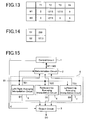
- Fig. 13 is a table showing values of determination data M1 and M2 of the test pixels T1 - T4 calculated as described above.
- the control circuit 1 adds up the determination data M1[T1] - M1[T4], and calculates the evaluation data S1 for evaluating the interpolation aptitude of the left/right averaging interpolation circuit 5.
- control circuit 1 adds up the determination data M2[T1] - M2[T4], and calculates the evaluation data S2 for evaluating the interpolation aptitude of the rightward up averaging interpolation circuit 6.
- Fig. 14 is a table showing the evaluation data S1 of the left/right averaging interpolation circuit 5 and the evaluation data S2 of the rightward up averaging interpolation circuit 6.
- the evaluation data S2 of the rightward up averaging interpolation circuit 6 has the smallest value.
- the original image data illustrated in Fig. 9 (a) has a rightward up outline
- the rightward up averaging interpolation circuit 6 is estimated to have the highest interpolation aptitude.
- the evaluation data shown in Fig. 14 also indicates that the rightward up averaging interpolation circuit 6 has the highest interpolation aptitude.
- the control circuit 1 selects the evaluation data S2, and specifies the rightward up averaging calculating circuit 6 corresponding to this evaluation data.
- the control circuit 1 sends the selection signal C for selecting the interpolation candidate data D2 for the lost pixel L calculated by the rightward up averaging interpolation circuit 6 to the output circuit 3.
- the interpolation pixel data can be accurately calculated using the most suitable interpolation method in accordance with an outline neighboring the interpolation pixel.
- Fig. 15 is a block diagram illustrating another configuration of the interpolation unit 4.
- the interpolation unit 4 of the pixel interpolation circuit illustrated in Fig. 1 includes a left/right averaging interpolation circuit 5, a rightward up averaging interpolation circuit 6, and a leftward up averaging interpolation circuit 7.
- the left/right averaging interpolation circuit 5 and the rightward up averaging interpolation circuit 6 calculate the test interpolation data and the interpolation candidate data using the methods described in the Embodiment 1.
- the leftward up averaging interpolation circuit 7 calculates average values of pixels located on the leftward up and rightward down positions of a pixel to be interpolated. In other words, the circuit calculates the average value "XL" of pixels "A" and "F” located on the leftward up and rightward down positions of the pixel L.
- the average value XL calculated by the leftward up averaging interpolation circuit 7 is represented by the following Formula (5), wherein data values (gradation values) of pixels A and F are represented as XA and XF, respectively.
- X L ( X A + X F ) / 2
- Fig. 16 is a pattern diagram illustrating another example of image data input into the interpolation circuit.
- non-lost pixels are represented with symbol “O” and symbol “ ⁇ "
- lost pixels are represented with symbol "X”.
- Fig. 16 (a) illustrates an original image
- Fig. 16 (b) illustrates a state in which pixels illustrated in a portion "LL” is lost.
- the original image in the lost portion LL represents a leftward up outline.
- the gradation value of each of the pixels is represented by 8 bit (0 - 255) data, and pixels illustrated as "O” has a gradation value 255, and pixels illustrated as " ⁇ ” has a gradation value 0.
- pixels T1 - T4 each located in the left and right sides of the lost pixel L are used as the test pixels.
- the leftward up averaging interpolation circuit 7 calculates test interpolation data TD3[T1] - TD3[T4] for the test pixels T1 - T4 illustrated in Fig. 16 (b), using the Formula (5).
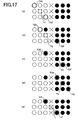
- Fig. 17 is a diagram for explaining methods for calculating the test interpolation data and the interpolation candidate data using the leftward up averaging interpolation circuit 7.
- the test interpolation data TD3[T1] for the test pixel T1 is obtained by calculating the average value of pixels "T1A” and "T1F” located on the leftward up and rightward down positions of the test pixel T1 as illustrated in Fig. 17 (a).
- the test interpolation data TD3[T2] for the test pixel T2 is obtained by calculating the average value of pixels "T2A” and "T2F" located on the leftward up and rightward down positions of the test pixel T2 as illustrated in Fig. 17 (b).
- the test interpolation data TD3[T3] for the test pixel T3 is obtained by calculating the average value of pixels "T3A” and "T3F" located on the leftward up and rightward down positions of the test pixel T3 as illustrated in Fig. 17 (c).
- the test interpolation data TD3[T4] for the test pixel T4 is obtained by calculating the average value of pixels "T4A” and "T4F" located on the leftward up and rightward down positions of the test pixel T4 as illustrated in Fig. 17 (d).
- the determination circuit 2 obtains the determination data M1[T1] - M1[T4] by calculating the absolute values of the differences between the test interpolation data TD3[T1] - TD3[T4] and the values DI[T1] - DI[T4] of the test pixels T1 - T4.
- 0
- the left/right averaging interpolation circuit 5 and the rightward up averaging interpolation circuit 6 calculate the interpolation candidate data D1 and D2 and the test interpolation data TD1[T1] - TD1[T4] and TD2[T1] - TD21[T4], and the determination circuit 2 calculates determination data M1[T1] - M1[T4] and M2[T1] - M2[T4] based on the test interpolation data.
- the processes in the left/right averaging interpolation circuit 5 and the rightward up averaging interpolation circuit 6 are described in the Embodiment 1.
- the interpolation candidate data D1 calculated by the left/right averaging interpolation circuit 5 is 127.5
- the interpolation candidate data D2 calculated by the rightward up averaging interpolation circuit 6 is 127.5.
- Fig. 18 is a table showing values of determination data M1, M2, and M3 for test pixels T1 - T4.
- the control circuit 1 adds up the determination data M1[T1] - M1[T4], and calculates the evaluation data S1 for evaluating the interpolation aptitude of the left/right averaging interpolation circuit 5.
- control circuit 1 adds up the determination data M2[T1] - M2[T4], and calculates the evaluation data S2 for evaluating the interpolation aptitude of the rightward up averaging interpolation circuit 6
- control circuit 1 adds up the determination data M3[T1] - M3[T4], and calculates the evaluation data S3 for evaluating the interpolation aptitude of the leftward up averaging interpolation circuit 7.
- Fig. 19 is a table showing values of the evaluation data S1, S2 and S3, which are calculated for the left/right averaging interpolation circuit 5, the rightward up averaging interpolation circuit 6, and the leftward up averaging interpolation circuit 7.
- the evaluation data S3 of the leftward up averaging interpolation circuit 7 has a smallest value.
- the leftward up averaging interpolation circuit 7 is estimated to have the highest interpolation aptitude.
- the evaluation data represented in Fig. 19 also indicates that the leftward up averaging interpolation circuit 7 has the highest interpolation aptitude.
- the control circuit 1 selects the minimal evaluation data S3, and specifies leftward up averaging interpolation circuit 7 corresponding to this evaluation data.
- the control circuit sends the selection signal C for selecting the interpolation candidate data D3 calculated by the leftward up averaging interpolation circuit 7 for the lost pixel L to the output circuit 3.
- the pixel interpolation circuit according to this invention can be used for increasing the number of pixels of an input image.
- the interpolation candidate data may be calculated using methods other than a left/right averaging interpolation, a rightward up average interpolation, or a leftward up average interpolation. For example such a method as calculating interpolation pixel using the least-square method, or calculating interpolation pixel data using a biquadratic curve obtained from four pixels neighboring the interpolation pixel can be used.
- a method as calculating interpolation pixel using the least-square method, or calculating interpolation pixel data using a biquadratic curve obtained from four pixels neighboring the interpolation pixel can be used.
- various kinds of interpolation circuits can further be added to the interpolation unit 4 without drastically modifying a configuration of the whole circuit.
- Data amount of the determination data to be processed in the determination circuit 2 may be increased when the number of the interpolation circuits composing the interpolation unit 4 is increased.
- the data amount of the determination data can be decreased, by binarizing or ternarizing the determination data using a predefined threshold value.
- the determination circuit 2 compares the absolute value of the difference between the test interpolation data TD1[T1] calculated by the first interpolation circuit 4a and the value DI[T1] of the test pixel T1, with two predefined threshold values TH1 and TH2 (0 ⁇ TH1 ⁇ TH2) .
- a value of the determination data M1[T1] is set -1;
- a value of the determination data is set 0; and when the absolute value is larger than the threshold value TH2, a value of the determination data is set 1.
- the determination circuit 2 similarly calculates the determination data M1[T2] - M1[Tm] for the test pixels T2 - Tm.
- the determination data M1[T1] - M1[Tm] calculated in the above described method represent error of the test interpolation data with three values, -1, 0, and 1.
- the determination data becomes -1 when the error is small.
- the determination circuit 2 similarly calculates the ternarized determination data MD2[T1] - MD2[Tm] for the test interpolation data TD2[T1] - TD2[Tm], ... TDn[T1] - TDn[Tm] calculated by the 2 nd -n th interpolation circuits 4b-4n.
- Fig. 20 is a table showing values of the ternarized determination data M1 and M2 for the test pixels T1 - T4.
- the control circuit 1 adds up the ternarized determination data M1[T1] -M1[T4], and calculates the evaluation data S1 for the left/right averaging interpolation circuit 5.
- control circuit 1 adds up the determination data M2[T1] - M2[T4], and calculates the evaluation data S2 for evaluating the rightward up averaging interpolation circuit 6.
- Fig. 21 is a table showing the evaluation data S1 of the left/right averaging interpolation circuit 5 and the evaluation data S2 of the rightward up averaging interpolation circuit 6.
- the evaluation data S2 calculated for the rightward up averaging interpolation circuit 6 has the smallest value. The smaller the difference between the test interpolation data and actual image data is, the smaller the evaluation data becomes.
- the original image data illustrated in Fig. 9 (a) represents a rightward up outline, the rightward up average interpolation circuit 6 is estimated to have high interpolation aptitude.
- the evaluation data S2 has the smallest value as shown in Fig. 14, indicating that the interpolation aptitude of the rightward up averaging interpolation circuit 6 is high, which means the interpolation method can be properly selected even if the determination data is ternarized.
- the determination data is ternarized using two threshold values.
- the data volume of the determination data can be also decreased by binarizing them using one threshold value or by decreasing the number of bits.
- the pixel interpolation circuit according to this invention may be configured by either hardware or software, or may be configured with both hardware and software being properly mixed.
Landscapes
- Engineering & Computer Science (AREA)
- Physics & Mathematics (AREA)
- General Physics & Mathematics (AREA)
- Theoretical Computer Science (AREA)
- Multimedia (AREA)
- Signal Processing (AREA)
- Image Processing (AREA)
- Facsimile Image Signal Circuits (AREA)
- Editing Of Facsimile Originals (AREA)
Abstract
Description
- This invention is related to an image processing method applied to an image scanner using an image sensor, and particularly to a method of generating interpolation pixel data for a digital image.
- In an image scanner using an image sensor, a pixel interpolation process is performed to interpolate a lost pixel. Interpolation pixel data is obtained by averaging pixel data neighboring the lost pixel, or calculating a regression line of pixels neighboring the lost pixel using a least-square method. Moreover, as described in Japanese a Laid-Open Open Patent Publication 2003-101724, the pixel interpolation data is also obtained by calculating a biquadratic curve of four pixels neighboring the interpolation pixel.
- There are various methods for obtaining the interpolation pixel data, however, a conventional pixel interpolation circuit has a following problem. Since the conventional pixel interpolation circuit calculates the interpolation pixel data using a fixedmethod without considering an image characteristic, for example, a difference between original pixels and interpolation pixels (interpolation error) becomes large in an image area forming outlines, and an image quality is deteriorated.
- The present invention has been made in order to solve above problems and to provide a pixel interpolation circuit, which is able to calculate an interpolation pixel data without causing the interpolation error for images having various characteristics.
- A pixel interpolation circuit according to this invention includes a plurality of interpolation circuits each calculating interpolation candidate data of a interpolation pixel and test interpolation data of a plurality of pixels neighboring the interpolation pixel using different interpolation methods, a determining circuit for selecting one of the interpolation circuits based on a difference between the test interpolation data and actual pixel data and an output circuit for outputting the interpolation candidate data calculated by the selected interpolation circuit as the interpolation pixel data.
- A pixel interpolation method according to this invention comprising calculating interpolation candidate data of a interpolation pixel and test interpolation data of a plurality of pixels neighboring the interpolation pixel, using different interpolation methods, selecting one of the interpolation methods based on a difference between the test interpolation data and actual pixel data, and outputting the interpolation candidate data calculated by the selected interpolation method as the interpolation pixel data.
-
- Fig. 1 is a block diagram illustrating a configuration of a pixel interpolation circuit according to this invention; Fig. 2 is a flow chart illustrating a process of a pixel interpolation calculation;
- Fig. 3 is a diagram illustrating an example of test pixels;
- Fig. 4 is a flow chart illustrating a calculation process of determination data;
- Fig. 5 is a table illustrating a relation between the test pixels and the determination data;
- Fig. 6 is a flow chart illustrating a calculation process of determination data;
- Fig. 7 is a table illustrating a relation between interpolation circuits and the determination data;
- Fig. 8 is a block diagram illustrating a configuration of a pixel interpolation circuit according to the invention;
- Fig. 9 is a diagram illustrating an example of original image data and input image data;
- Fig. 10 is a diagram for explaining an interpolation calculation;
- Fig. 11 is a diagram for explaining methods for calculating test interpolation data and interpolation candidate data using a left/right averaging interpolation circuit;
- Fig. 12 is a diagram for explaining methods for calculating test interpolation data and interpolation candidate data using a rightward up averaging interpolation circuit;
- Fig. 13 is a table illustrating values of determination data M1 and M2;
- Fig. 14 is a table illustrating values of evaluation data S1 and S2;
- Fig. 15 is a block diagram illustrating a configuration of a pixel interpolation circuit according to the invention; Fig. 16 is a diagram illustrating an example of original image data and input image data;
- Fig. 17 is a diagram for explaining methods for calculating test interpolation data and interpolation candidate data using a leftward up averaging interpolation circuit;
- Fig. 18 is a table illustrating values of determination data M1 - M4;
- Fig. 19 is a table illustrating values of evaluation data S1 - S3;
- Fig. 20 is a table illustrating values of determination data M1 and M2; and
- Fig. 21 is a table illustrating values of evaluation data S1 - S3.
- Fig. 1 is a block diagram illustrating a configuration of a pixel interpolation circuit according to this invention. The pixel interpolation circuit illustrated in Fig. 1 includes a
control circuit 1, adetermination circuit 2, anoutput circuit 3, and aninterpolation unit 4. Theinterpolation unit 4 includes 1st-nth interpolation circuits 4a-4n (n is an integer greater than 2), each of which performs different interpolation processes. Image data DI read by a scanner or a copy machine is sent to thedetermination circuit 2 and theinterpolation unit 4. The image data DI sent to theinterpolation unit 4, is sent to each of the 1st-nth interpolation circuits 4a-4n. Fig. 2 is a flow chart illustrating a process of the pixel interpolation performed by the pixel interpolation circuit illustrated in Fig. 1. - Firstly, in the 1st
interpolation circuit 4a, a test interpolation calculation is performed over pixels T1-Tm (hereinafter, referred to as test pixels) neighboring one of lost pixels included in the image data DI so as to calculate test interpolation data TD1[T1] - TD1[Tm] (Step 1). - Fig. 3 is a pattern diagram illustrating an example of lost pixels and test pixels. In Fig.3, lost pixels are represented with symbol "X", and non-lost pixels are represented with symbol "○ ". "L" is one of the lost pixels to be interpolated, and non-lost pixels T1 - Tm (m = 2 x k) neighboring the lost pixel are used as the test pixels. Fig. 3 (a) illustrates an example in which the non-lost pixels T1 - Tm located in left and right sides of the lost pixel L are used as the test pixels. Fig. 3 (b) illustrates an example in which non-lost pixels located in left and right sides of the lost pixel L in both vertical and horizontal directions are used as the test pixels.
- The test interpolation calculation is performed by calculating interpolation pixel data for each of the test pixels on the assumption that the test pixels T1 - Tm are lost. For example, the test interpolation data TD1[T1] of the test pixel T1 is obtained by calculating an interpolation pixel data using the non-lost pixels neighboring the test pixel T1.
- The test interpolation data TD1[T1] - TD1[Tm] (indicated as TD1 in Fig.1) calculated by the 1st
interpolation circuit 4a is sent to thedetermination circuit 2. Thedetermination circuit 2 calculates determination data M1[T1] - M1[Tm] that represent differences between the test interpolation data TD1[T1] - TD1[Tm] and data values DI[T1] - DI[Tm] of the test pixels T1-Tm (Step 2). The determination data M1[T1] - M1[Tm] is sent to thecontrol circuit 1. - When the test interpolation data TD1[Tm] and the determination data M1[T1] - M1[Tm] are calculated for the last test pixel Tm (Step 3), the
first interpolation circuit 4a performs an interpolation calculation over the lost pixel L, so as to calculate an interpolation candidate data D1 (Step 4). The interpolation candidate data D1 is sent to theoutput circuit 3. - The above-described processes of Step 1 -
Step 4 are similarly performed in the 2nd-nth interpolation circuits 4b-4n (Step 5). In other words, the test interpolation data, TD2[T1] - TD2[Tm], ... TDn[T1] - TDn[Tm] (indicated as TD2 - TDn in Fig.1), are calculated in the 2nd-nth interpolation circuits 4b-4n and sent to thedetermination circuit 2. Thedetermination circuit 2 calculates the determination data, M2[T1] - M2[Tm], ... Mn[T1] - Mn[Tm], for the test interpolation data TD2 - TDn. Then, interpolation candidate data D2 - Dn for the lost pixel L are calculated in the 2nd-nth interpolation circuits 4b-4n and send to theoutput circuit 3. - Fig. 4 is a flow chart illustrating a calculation process of the determination data in
Step 2. - The
determination circuit 2 calculates the absolute values of the differences between the test interpolation data TD1[T1] - TD1[Tm] and the values DI[T1] - DI[Tm] of the test pixels T1 - Tm (Step 21), respectively, and outputs the absolute values as the determination data M1[T1] - M1[Tm] (Step 22) . The determination data M1[T1] - M1[Tm] are calculated using the following Formulas (1).
Formulas (1):
- The
determination circuit 2 also performs processes of Step 21 and Step 22 for the test interpolation data, TD2[T1] - TD2[Tm], ... TDn[T1] - TDn[Tm], calculated by the 2nd-nth interpolation circuits 4b-4n, so as to calculate the determination data M2[T1] - M2[Tm], ... Mn[T1] - Mn[Tm]. - Fig. 5 is a table representing all the determination data calculated by the
determination circuit 2. As sown in Fig. 5, the determination data is calculated for each of the nxm test interpolation data of the test pixels T1 - Tm calculated by the 1st-nth interpolation circuits 4a-4n. - Next, the determination data M1[T1] - M1[Tm], ... Mn[T1] - Mn[Tm] are evaluated in the control circuit 1 (Step 6).
- Fig. 6 is a flow chart illustrating a process of evaluating determination data in
Step 6. - Firstly, the
control circuit 1 calculates evaluation data S1 for the 1stinterpolation circuit 4a by summing up the determination data M1[T1] - M1[Tm] (Step 61) . - The
control circuit 1 similarly calculates evaluation data S2 - Sn for the 2nd-nth interpolation circuits 4b-4n (Step 62). - Calculations of the evaluation data S1 - Sn are represented by the following Formulas (2).
Formulas (2):
- Fig. 7 is a diagram showing relations between the 1st-nth interpolation circuits 4b-4n and the evaluation data S1 - Sn.
- Next, the control circuit selects minimal evaluation data Sx from the evaluation data S1 - Sn (Step 63), and then specifies an
interpolation circuit 4x corresponding to the evaluation data Sx (Step 64) . The smaller a difference between the test interpolation data and actual image data is, the smaller the evaluation data becomes. Therefore, theinterpolation circuit 4x with the smallest evaluation data is estimated to have highest interpolation aptitude, which means the interpolation error becomes smallest. Thecontrol circuit 1 sends a selection signal C for selecting interpolation candidate data Dx calculated by theinterpolation circuit 4x to the output circuit 3 (Step 65). - The
output circuit 3 selects the interpolation candidate data Dx according to the selection signal C, and outputs as interpolation data DO (Step 7). - The processes of Step 1 -
Step 7 are performed for all the lost pixels to calculate interpolation pixel data DO. - Fig. 8 is a block diagram illustrating a detailed configuration of the
pixel interpolation unit 4 according to the invention. Theinterpolation unit 4 illustrated in Fig. 8 includes a left/right averaginginterpolation circuit 5 and a rightward up averaginginterpolation circuit 6. - Fig. 10 is a diagram for explaining an interpolation method of the left/right averaging
interpolation circuit 5 and the rightward up averaginginterpolation circuit 6. In Fig. 10, "L" represents a lost pixel to be interpolated by an interpolation calculation, and pixels "A"-"F" represent pixels neighboring the lost pixel L. - The left/right averaging
interpolation circuit 5 calculates an average value XL of pixels B and E located in left and right sides of the lost pixel L, and the rightward up averaginginterpolation circuit 6 calculates an average value of pixels D and C. The average values XL calculated by the left/right averaginginterpolation circuit 5 and the rightward up averaginginterpolation circuit 6 are represented by the following Formulas (3) and (4), wherein data values (gradation values) of the pixels A- F are represented as XA - XF, respectively.

- Fig. 9 is a pattern diagram illustrating an example of image data input into the interpolation circuit. In Figs. 9, non-lost pixels are represented with symbol "O" and symbol "●", and lost pixels are represented with symbol "×". Fig. 9(a) illustrates an original image, and Fig. 9 (b) illustrates a state in which pixels illustrated in a portion "LL" is lost. The original image in the lost portion LL represents a rightward up outline. The gradation value of each of the pixels is represented by 8 bit (0 - 255) data, and pixels illustrated as "○" has a
gradation value 255, and pixels illustrated as "●" has agradation value 0. - Hereinafter, a process of calculating an interpolation pixel data of the lost pixel L illustrated in Fig. 9 (b) is explained. Here, as illustrated in Fig. 9 (b), pixels T1 - T4 each located in the left and right sides of the lost pixel L are used as the test pixels.
- The left/right averaging
interpolation circuit 5 calculates test interpolation data TD1[T1] - TD1[T4] for the test pixels T1 - T4 illustrated in Fig. 9 (b), using the Formula (3). - Fig. 11 is a diagram for explaining methods for calculating test interpolation data and interpolation candidate data using the left/right averaging
interpolation circuit 5. - The test interpolation data TD1[T1] for the test pixel T1 is obtained by calculating the average value of pixels "T1B" and "T1E" located in left and right sides of the test pixel T1 as illustrated in Fig. 11 (a).
- The test interpolation data TD1[T2] for the test pixel T2 is obtained by calculating the average value of pixels "T2B" and "T2E" located in left and right sides of the test pixel T2 as illustrated in Fig. 11 (b).
- The test interpolation data TD1[T3] for the test pixel T3 is obtained by calculating the average value of pixels "T3B" and "T3E" located in left and right sides of the test pixel T3 as illustrated in Fig. 11 (c).
- The test interpolation data TD1[T4] for the test pixel T4 is obtained by calculating the average value of pixels "T4B" and "T4E" located in left and right sides of the test pixel T4 as illustrated in Fig. 11 (d).
- Therefore, the test interpolation data TD1[T1] - TD1[T4] are calculated as follows;


- As illustrated in Fig. 11 (e), the interpolation candidate data D1 is calculated by averaging pixels LB and LE on the left and right sides of the lost pixel L as follows;

- The
determination circuit 2 obtains the determination data M1[T1] -M1[T4] by calculating the absolute values of the differences between the test interpolation data TD1[T1] - TD1[T4] and the values DI[T1] - DI[T4] of the test pixels T1 - T4. - The determination data M1[T1] - M1[T4] are calculated as follows.



- The rightward up averaging
interpolation circuit 6 calculates test interpolation data TD1[T1] - TD1[T4] for the test pixels T1 - T4 illustrated in Fig. 9 (b), using Formula (4). - Figs. 12 are diagrams for explaining methods for calculating test interpolation data and interpolation candidate data using the rightward up averaging
interpolation circuit 6. - The test interpolation data TD2[T1] for the test pixel T1 is obtained by calculating the average value of pixels "T1D" and "T1C" located in upper right and lower left positions of the test pixel T1 as illustrated in Fig. 12 (a).
- The test interpolation data TD2[T2] for the test pixel T2 is obtained by calculating the average value of pixels "T2D" and "T2C" located on the rightward up and leftward down positions of the test pixel T2 as illustrated in Fig. 12 (b).
- The test interpolation data TD2[T3] for the test pixel T3 is obtained by calculating the average value of pixels "T3D" and "T3C" located on the rightward up and leftward down positions of the test pixel T3 as illustrated in Fig. 12 (c).
- The test interpolation data TD2[T4] for the test pixel T4 is obtained by calculating the average value of pixels "T4D" and "T4C" located on the rightward up and leftward down positions of the test pixel T4 as illustrated in Fig. 12 (d).
- Therefore, the test interpolation data TD1[T1] - TD1[T4] is calculated as follows;


- As illustrated in Fig. 12 (e), the interpolation candidate data D2 is calculated by averaging pixels LD and LC located on the rightward up and leftward down positions of the lost pixel L as follows;

- The
determination circuit 2 obtains the determination data M2[T1] - M2[T4] by calculating the absolute values of the differences between the test interpolation data TD2[T1] - TD2[T4] and the values DI[T1] - DI[T4] of the test pixels T1 - T4. - The determination data M2[T1] - M2[T4] is calculated as follows;




- Fig. 13 is a table showing values of determination data M1 and M2 of the test pixels T1 - T4 calculated as described above.
- The
control circuit 1 adds up the determination data M1[T1] - M1[T4], and calculates the evaluation data S1 for evaluating the interpolation aptitude of the left/right averaginginterpolation circuit 5. - The evaluation data S1 is given as follows;

- In a similar way, the
control circuit 1 adds up the determination data M2[T1] - M2[T4], and calculates the evaluation data S2 for evaluating the interpolation aptitude of the rightward up averaginginterpolation circuit 6. - The evaluation data S2 is given as follows;

- Fig. 14 is a table showing the evaluation data S1 of the left/right averaging
interpolation circuit 5 and the evaluation data S2 of the rightward up averaginginterpolation circuit 6. As illustrated in Fig. 14, the evaluation data S2 of the rightward up averaginginterpolation circuit 6 has the smallest value. As described above, the smaller the difference between the test interpolation data and actual image data is, the smaller the evaluation data becomes. Because the original image data illustrated in Fig. 9 (a) has a rightward up outline, the rightward up averaginginterpolation circuit 6 is estimated to have the highest interpolation aptitude. The evaluation data shown in Fig. 14 also indicates that the rightward up averaginginterpolation circuit 6 has the highest interpolation aptitude. - The
control circuit 1 selects the evaluation data S2, and specifies the rightward up averaging calculatingcircuit 6 corresponding to this evaluation data. Thecontrol circuit 1 sends the selection signal C for selecting the interpolation candidate data D2 for the lost pixel L calculated by the rightward up averaginginterpolation circuit 6 to theoutput circuit 3. - According to the selection signal C, the
output circuit 3 outputs the interpolation candidate data D2 (D2 = 0) calculated by the rightward up averaginginterpolation circuit 6 as the interpolation pixel data DO (DO = 0). - As illustrated in Figs. 9, a data value of the lost pixel L in the original image is 0, which means that the interpolation candidate data D2 (D2 = 0) calculated by the rightward up averaging
interpolation circuit 6 has smaller error than the interpolation candidate data D1 (D1 = 127.5) calculated by the left/right averaginginterpolation circuit 5. - As described above, by selecting the interpolation candidate data calculated by the different interpolation methods, based on the results of the test interpolation calculations, the interpolation pixel data can be accurately calculated using the most suitable interpolation method in accordance with an outline neighboring the interpolation pixel.
- Fig. 15 is a block diagram illustrating another configuration of the
interpolation unit 4. Theinterpolation unit 4 of the pixel interpolation circuit illustrated in Fig. 1 includes a left/right averaginginterpolation circuit 5, a rightward up averaginginterpolation circuit 6, and a leftward up averaginginterpolation circuit 7. The left/right averaginginterpolation circuit 5 and the rightward up averaginginterpolation circuit 6 calculate the test interpolation data and the interpolation candidate data using the methods described in theEmbodiment 1. - The leftward up averaging
interpolation circuit 7 calculates average values of pixels located on the leftward up and rightward down positions of a pixel to be interpolated. In other words, the circuit calculates the average value "XL" of pixels "A" and "F" located on the leftward up and rightward down positions of the pixel L. The average value XL calculated by the leftward up averaginginterpolation circuit 7 is represented by the following Formula (5), wherein data values (gradation values) of pixels A and F are represented as XA and XF, respectively.
- Fig. 16 is a pattern diagram illustrating another example of image data input into the interpolation circuit. In Figs. 16, non-lost pixels are represented with symbol "O" and symbol "● ", and lost pixels are represented with symbol "X". Fig. 16 (a) illustrates an original image, and Fig. 16 (b) illustrates a state in which pixels illustrated in a portion "LL" is lost. The original image in the lost portion LL represents a leftward up outline. The gradation value of each of the pixels is represented by 8 bit (0 - 255) data, and pixels illustrated as "O" has a
gradation value 255, and pixels illustrated as "●" has agradation value 0. - Hereinafter, processes of calculating interpolation pixel data of the lost pixel L illustrated in Fig. 16 (b) are explained. Here, as illustrated in Fig. 16 (b), pixels T1 - T4 each located in the left and right sides of the lost pixel L are used as the test pixels.
- The leftward up averaging
interpolation circuit 7 calculates test interpolation data TD3[T1] - TD3[T4] for the test pixels T1 - T4 illustrated in Fig. 16 (b), using the Formula (5). - Fig. 17 is a diagram for explaining methods for calculating the test interpolation data and the interpolation candidate data using the leftward up averaging
interpolation circuit 7. - The test interpolation data TD3[T1] for the test pixel T1 is obtained by calculating the average value of pixels "T1A" and "T1F" located on the leftward up and rightward down positions of the test pixel T1 as illustrated in Fig. 17 (a).
- The test interpolation data TD3[T2] for the test pixel T2 is obtained by calculating the average value of pixels "T2A" and "T2F" located on the leftward up and rightward down positions of the test pixel T2 as illustrated in Fig. 17 (b).
- The test interpolation data TD3[T3] for the test pixel T3 is obtained by calculating the average value of pixels "T3A" and "T3F" located on the leftward up and rightward down positions of the test pixel T3 as illustrated in Fig. 17 (c).
- The test interpolation data TD3[T4] for the test pixel T4 is obtained by calculating the average value of pixels "T4A" and "T4F" located on the leftward up and rightward down positions of the test pixel T4 as illustrated in Fig. 17 (d).
- Therefore, the test interpolation data TD3[T1] - TD3[T4] are calculated as follows;


- As illustrated in Fig. 17 (e), the interpolation candidate data D3 is calculated by averaging pixels LA and LF located on the leftward up and rightward down positions of the lost pixel L as follows;

- The
determination circuit 2 obtains the determination data M1[T1] - M1[T4] by calculating the absolute values of the differences between the test interpolation data TD3[T1] - TD3[T4] and the values DI[T1] - DI[T4] of the test pixels T1 - T4. - The determination data M3[T1] through M3[T4] can be calculated as follows;


- The left/right averaging
interpolation circuit 5 and the rightward up averaginginterpolation circuit 6 calculate the interpolation candidate data D1 and D2 and the test interpolation data TD1[T1] - TD1[T4] and TD2[T1] - TD21[T4], and thedetermination circuit 2 calculates determination data M1[T1] - M1[T4] and M2[T1] - M2[T4] based on the test interpolation data. The processes in the left/right averaginginterpolation circuit 5 and the rightward up averaginginterpolation circuit 6 are described in theEmbodiment 1. - Here, the interpolation candidate data D1 calculated by the left/right averaging
interpolation circuit 5 is 127.5, and the interpolation candidate data D2 calculated by the rightward up averaginginterpolation circuit 6 is 127.5. - Fig. 18 is a table showing values of determination data M1, M2, and M3 for test pixels T1 - T4.
- The
control circuit 1 adds up the determination data M1[T1] - M1[T4], and calculates the evaluation data S1 for evaluating the interpolation aptitude of the left/right averaginginterpolation circuit 5. - The evaluation data S1 is given as follows;

- In a similar way, the
control circuit 1 adds up the determination data M2[T1] - M2[T4], and calculates the evaluation data S2 for evaluating the interpolation aptitude of the rightward up averaginginterpolation circuit 6 - The evaluation data S2 is given as follows;

- In a similar way, the
control circuit 1 adds up the determination data M3[T1] - M3[T4], and calculates the evaluation data S3 for evaluating the interpolation aptitude of the leftward up averaginginterpolation circuit 7. - The evaluation data S3 is given as follows;

- Fig. 19 is a table showing values of the evaluation data S1, S2 and S3, which are calculated for the left/right averaging
interpolation circuit 5, the rightward up averaginginterpolation circuit 6, and the leftward up averaginginterpolation circuit 7. As illustrated in Fig. 19, the evaluation data S3 of the leftward up averaginginterpolation circuit 7 has a smallest value. As described above, the smaller the difference between the test interpolation data and actual image data is, the lower the evaluation data becomes. Because the original image data illustrated in Fig. 16 (a) has a rightward up outline, the leftward up averaginginterpolation circuit 7 is estimated to have the highest interpolation aptitude. The evaluation data represented in Fig. 19 also indicates that the leftward up averaginginterpolation circuit 7 has the highest interpolation aptitude. - The
control circuit 1 selects the minimal evaluation data S3, and specifies leftward up averaginginterpolation circuit 7 corresponding to this evaluation data. The control circuit sends the selection signal C for selecting the interpolation candidate data D3 calculated by the leftward up averaginginterpolation circuit 7 for the lost pixel L to theoutput circuit 3. - According to the selection signal C, the
output circuit 3 outputs the interpolation candidate data D3 (D3 = 0) calculated by the leftward up averaginginterpolation circuit 7 as the interpolation pixel data DO (DO = 0). - As illustrated in Figs. 16, a data value of the lost pixel L in the original image is 0, which means that the interpolation candidate data D3 (D3 = 0) calculated by the leftward up averaging
interpolation circuit 7 has smaller error than the interpolation candidate data D1 (D1 = 127.5) calculated by the left/right averaginginterpolation circuit 5 or the interpolation candidate data D2 (D2 = 127.5) calculated by the rightward up averaginginterpolation circuit 6. - As described above, by further providing the leftward up averaging
interpolation circuit 7, more accurate interpolation process can be realized. In other words, the most suitable interpolationmethod is used for an image having different characteristics. Furthermore, the pixel interpolation circuit according to this invention can be used for increasing the number of pixels of an input image. - In the
interpolation unit 4, the interpolation candidate data may be calculated using methods other than a left/right averaging interpolation, a rightward up average interpolation, or a leftward up average interpolation. For example such a method as calculating interpolation pixel using the least-square method, or calculating interpolation pixel data using a biquadratic curve obtained from four pixels neighboring the interpolation pixel can be used. In the pixel interpolation circuit according to this invention, various kinds of interpolation circuits can further be added to theinterpolation unit 4 without drastically modifying a configuration of the whole circuit. - Data amount of the determination data to be processed in the
determination circuit 2 may be increased when the number of the interpolation circuits composing theinterpolation unit 4 is increased. The data amount of the determination data can be decreased, by binarizing or ternarizing the determination data using a predefined threshold value. - As an example, a method of ternarizing the determination data values will be explained.
- The
determination circuit 2 compares the absolute value of the difference between the test interpolation data TD1[T1] calculated by thefirst interpolation circuit 4a and the value DI[T1] of the test pixel T1, with two predefined threshold values TH1 and TH2 (0 ≤ TH1 < TH2) . When the absolute value is smaller than the threshold value TH1, a value of the determination data M1[T1] is set -1; when the absolute value is larger than the threshold value TH1 and smaller than the threshold value TH2, a value of the determination data is set 0; and when the absolute value is larger than the threshold value TH2, a value of the determination data is set 1. - That is:


- The
determination circuit 2 similarly calculates the determination data M1[T2] - M1[Tm] for the test pixels T2 - Tm. - That is:




...


- The determination data M1[T1] - M1[Tm] calculated in the above described method represent error of the test interpolation data with three values, -1, 0, and 1. The determination data becomes -1 when the error is small.
- The
determination circuit 2 similarly calculates the ternarized determination data MD2[T1] - MD2[Tm] for the test interpolation data TD2[T1] - TD2[Tm], ... TDn[T1] - TDn[Tm] calculated by the 2nd-nth interpolation circuits 4b-4n. - Hereinafter, a process of calculating ternarized determination data in the pixel interpolation circuit illustrated in Fig. 8 will be explained. In the following explanation, the interpolation pixel data for the lost pixel L illustrated in Fig. 9 (b) will be calculated, and the threshold values TH1=50 and TH2=100 will be used.
- As calculated in
Embodiment 1, the absolute values of the differences between the test interpolation data TD1[T1] - TD1[T4] and the values DI[T1] - DI[T4] of the test pixels T1 - T4 are given as follows;



- Relations between these absolute values and the threshold values TH1 (TH1 = 50) and TH2 (TH1 = 100) are shown as follows;


- Therefore, the determination data calculated for the left/right averaging
interpolation circuit 5 are given as follows;


- The absolute values of the differences between the test interpolation data TD1[T1] - TD1[T4] calculated by the rightward up averaging
interpolation circuit 6 and the values DI[T1] - DI[T4] of the test pixels T1 - T4 are given as follows;


- Relations between these absolute values and the threshold values TH1 (TH1 = 50) and TH2 (TH1 = 100) are given as follows;


- Therefore, the determination data calculated for the rightward up averaging
interpolation circuit 6 are given as follows;


- Fig. 20 is a table showing values of the ternarized determination data M1 and M2 for the test pixels T1 - T4.
- The
control circuit 1 adds up the ternarized determination data M1[T1] -M1[T4], and calculates the evaluation data S1 for the left/right averaginginterpolation circuit 5. - The evaluation data S1 is given as follows;


- Similarly, the
control circuit 1 adds up the determination data M2[T1] - M2[T4], and calculates the evaluation data S2 for evaluating the rightward up averaginginterpolation circuit 6. - The evaluation data S2 is given as follows;

- Fig. 21 is a table showing the evaluation data S1 of the left/right averaging
interpolation circuit 5 and the evaluation data S2 of the rightward up averaginginterpolation circuit 6. As shown in Fig. 21, the evaluation data S2 calculated for the rightward up averaginginterpolation circuit 6 has the smallest value. The smaller the difference between the test interpolation data and actual image data is, the smaller the evaluation data becomes. Because, the original image data illustrated in Fig. 9 (a) represents a rightward up outline, the rightward upaverage interpolation circuit 6 is estimated to have high interpolation aptitude. The evaluation data S2 has the smallest value as shown in Fig. 14, indicating that the interpolation aptitude of the rightward up averaginginterpolation circuit 6 is high, which means the interpolation method can be properly selected even if the determination data is ternarized. - In the above explanation, the determination data is ternarized using two threshold values. The data volume of the determination data can be also decreased by binarizing them using one threshold value or by decreasing the number of bits.
- The pixel interpolation circuit according to this invention may be configured by either hardware or software, or may be configured with both hardware and software being properly mixed.
Claims (7)
- A pixel interpolation circuit for generating interpolation pixel data which interpolates an input image based on pixel data composing the input image, the pixel interpolation circuit comprising:a plurality of interpolation circuits each calculating interpolation candidate data of a interpolation pixel and test interpolation data of a plurality of pixels neighboring the interpolation pixel, using different interpolation methods;a determining circuit for selecting one of the interpolation circuits based on a difference between the test interpolation data and actual pixel data; andan output circuit for outputting the interpolation candidate data calculated by the selected interpolation circuit as the interpolation pixel data.
- A pixel interpolation circuit according to claim 1, wherein the determining circuit calculates a evaluation data for each of the interpolation circuits, by summing up the absolute values of the difference between the test interpolation data and the actual pixel data, and selects one of the interpolation circuits based on the evaluation data.
- A pixel interpolation circuit according to claim 1, wherein the determining circuit calculates binarized or ternarized values of the difference between the test interpolation data and the actual pixel data.
- A pixel interpolation method for generating interpolation pixel data which interpolates an input image based on pixel data composing the input image, the pixel interpolation method comprising:calculating interpolation candidate data of a interpolation pixel and test interpolation data of a plurality of pixels neighboring the interpolation pixel, using different interpolation methods;selecting one of the interpolation methods based on a difference between the test interpolation data and actual pixel data; andoutputting the interpolation candidate data calculated by the selected interpolation method as the interpolation pixel data.
- A pixel interpolation method according to claim 4 further comprising,calculating a evaluation data for each of the interpolation methods, by summing up the absolute values of the difference between the test interpolation data and the actual pixel data, wherein the interpolation method is selected based on the evaluation data.
- A pixel interpolation circuit according to claim 4 further comprising,calculating binarized or ternarized values of the difference between the test interpolation data and the actual pixel data.
- An image scanner comprising a pixel interpolation circuit according to claims 1.
Applications Claiming Priority (2)
| Application Number | Priority Date | Filing Date | Title |
|---|---|---|---|
| JP2003347944A JP3767593B2 (en) | 2003-10-07 | 2003-10-07 | Pixel interpolation circuit and pixel interpolation method |
| PCT/JP2004/009179 WO2005036868A1 (en) | 2003-10-07 | 2004-06-30 | Pixel interpolation circuit and pixel interpolation method, and image reader |
Publications (2)
| Publication Number | Publication Date |
|---|---|
| EP1672907A1 true EP1672907A1 (en) | 2006-06-21 |
| EP1672907A4 EP1672907A4 (en) | 2007-04-25 |
Family
ID=34430942
Family Applications (1)
| Application Number | Title | Priority Date | Filing Date |
|---|---|---|---|
| EP04746648A Withdrawn EP1672907A4 (en) | 2003-10-07 | 2004-06-30 | PIXEL INTERPOLATION CIRCUIT, PIXEL INTERPOLATION METHOD, AND IMAGE READER |
Country Status (6)
| Country | Link |
|---|---|
| US (1) | US20060050990A1 (en) |
| EP (1) | EP1672907A4 (en) |
| JP (1) | JP3767593B2 (en) |
| CN (1) | CN100334873C (en) |
| TW (1) | TWI257588B (en) |
| WO (1) | WO2005036868A1 (en) |
Cited By (1)
| Publication number | Priority date | Publication date | Assignee | Title |
|---|---|---|---|---|
| EP2242019A1 (en) * | 2009-04-15 | 2010-10-20 | Mitsubishi Electric R&D Centre Europe B.V. | Image region interpolation |
Families Citing this family (11)
| Publication number | Priority date | Publication date | Assignee | Title |
|---|---|---|---|---|
| JP4775221B2 (en) * | 2006-10-02 | 2011-09-21 | コニカミノルタホールディングス株式会社 | Image processing apparatus, image processing apparatus control method, and image processing apparatus control program |
| JP4900025B2 (en) * | 2007-05-08 | 2012-03-21 | 富士ゼロックス株式会社 | Image processing apparatus and image processing program |
| JP4772754B2 (en) | 2007-06-25 | 2011-09-14 | 三菱電機株式会社 | Image interpolation apparatus and method, and image reading apparatus |
| US8559762B2 (en) | 2007-12-28 | 2013-10-15 | Nikon Corporation | Image processing method and apparatus for interpolating defective pixels |
| JP2010061565A (en) | 2008-09-05 | 2010-03-18 | Konica Minolta Business Technologies Inc | Pixel interpolation device, pixel interpolating method, and image reader |
| JP4958056B2 (en) * | 2009-05-12 | 2012-06-20 | 東芝ディーエムエス株式会社 | Image interpolation apparatus and image interpolation program |
| WO2012021502A2 (en) * | 2010-08-09 | 2012-02-16 | Board Of Regents, The University Of Texas System | Using higher order statistics to estimate pixel values in digital image processing to improve accuracy and computation efficiency |
| JP5741007B2 (en) | 2011-01-21 | 2015-07-01 | 株式会社リコー | Image processing apparatus, pixel interpolation method, and program |
| US10171770B2 (en) * | 2014-05-09 | 2019-01-01 | Maxell, Ltd. | Image playback device, display device, and transmission device |
| US11748852B2 (en) | 2018-06-27 | 2023-09-05 | Mitsubishi Electric Corporation | Pixel interpolation device and pixel interpolation method, and image processing device, and program and recording medium |
| KR102132690B1 (en) * | 2019-01-30 | 2020-07-13 | 인천대학교 산학협력단 | System for Reconstructing Image Super Resolution |
Family Cites Families (28)
| Publication number | Priority date | Publication date | Assignee | Title |
|---|---|---|---|---|
| JPS63122385A (en) * | 1986-11-11 | 1988-05-26 | Nec Corp | Picture signal band compressing system |
| US5430811A (en) * | 1991-12-25 | 1995-07-04 | Matsushita Electric Industrial Co., Ltd. | Method for interpolating missing pixels and an apparatus employing the method |
| US5418714A (en) * | 1993-04-08 | 1995-05-23 | Eyesys Laboratories, Inc. | Method and apparatus for variable block size interpolative coding of images |
| JP3125124B2 (en) * | 1994-06-06 | 2001-01-15 | 松下電器産業株式会社 | Defective pixel damage correction circuit |
| JPH08321944A (en) * | 1995-05-25 | 1996-12-03 | Kokusai Electric Co Ltd | Image data interpolation method |
| US5917963A (en) * | 1995-09-21 | 1999-06-29 | Canon Kabushiki Kaisha | Image processing apparatus and image processing method |
| KR970049856A (en) * | 1995-12-30 | 1997-07-29 | 김광호 | Sensor distance correction method and circuit in an image reading device having a plurality of licensors |
| MY117289A (en) * | 1996-01-17 | 2004-06-30 | Sharp Kk | Image data interpolating apparatus |
| JP3706189B2 (en) * | 1996-03-15 | 2005-10-12 | 富士写真フイルム株式会社 | Image data interpolation processing method and apparatus using the method |
| JP3503372B2 (en) * | 1996-11-26 | 2004-03-02 | ミノルタ株式会社 | Pixel interpolation device and pixel interpolation method |
| US6075926A (en) * | 1997-04-21 | 2000-06-13 | Hewlett-Packard Company | Computerized method for improving data resolution |
| US6002812A (en) * | 1997-07-10 | 1999-12-14 | Samsung Electronics Co., Ltd. | Interpolation method for binary image |
| US6563538B1 (en) * | 1997-09-26 | 2003-05-13 | Nikon Corporation | Interpolation device, process and recording medium on which interpolation processing program is recorded |
| JPH11122626A (en) * | 1997-10-17 | 1999-04-30 | Nikon Corp | Image processing method and apparatus, and recording medium storing image processing program |
| JP4066484B2 (en) * | 1997-12-08 | 2008-03-26 | ソニー株式会社 | Image processing apparatus, image processing method, and camera |
| EP1001353A1 (en) * | 1998-11-10 | 2000-05-17 | Sony Corporation | Interpolation apparatus and methods and image display apparatus |
| JP2001024883A (en) * | 1999-07-07 | 2001-01-26 | Fuji Photo Film Co Ltd | Picture processor, method for controlling it, and recording medium |
| JP3644874B2 (en) * | 1999-07-15 | 2005-05-11 | シャープ株式会社 | Image interpolation device |
| US7039254B1 (en) * | 1999-08-05 | 2006-05-02 | Sanyo Electric Co., Ltd. | Image interpolating method |
| JP2001307079A (en) * | 2000-04-26 | 2001-11-02 | Seiko Epson Corp | Image processing apparatus, image processing method, and recording medium |
| JP2002027325A (en) * | 2000-07-04 | 2002-01-25 | Victor Co Of Japan Ltd | Apparatus and method for correcting defective pixel |
| JP2002165092A (en) * | 2000-11-24 | 2002-06-07 | Canon Inc | Image processing apparatus and image processing method |
| US6900836B2 (en) * | 2001-02-19 | 2005-05-31 | Eastman Kodak Company | Correcting defects in a digital image caused by a pre-existing defect in a pixel of an image sensor |
| JP2003078821A (en) * | 2001-08-31 | 2003-03-14 | Hitachi Kokusai Electric Inc | Imaging device |
| US7245326B2 (en) * | 2001-11-19 | 2007-07-17 | Matsushita Electric Industrial Co. Ltd. | Method of edge based interpolation |
| KR100400018B1 (en) * | 2001-12-29 | 2003-09-29 | 삼성전자주식회사 | Apparatus and method for deleting sawtooth |
| US7136541B2 (en) * | 2002-10-18 | 2006-11-14 | Sony Corporation | Method of performing sub-pixel based edge-directed image interpolation |
| US7242819B2 (en) * | 2002-12-13 | 2007-07-10 | Trident Microsystems, Inc. | Method and system for advanced edge-adaptive interpolation for interlace-to-progressive conversion |
-
2003
- 2003-10-07 JP JP2003347944A patent/JP3767593B2/en not_active Expired - Lifetime
-
2004
- 2004-06-30 CN CNB2004800019233A patent/CN100334873C/en not_active Expired - Fee Related
- 2004-06-30 EP EP04746648A patent/EP1672907A4/en not_active Withdrawn
- 2004-06-30 WO PCT/JP2004/009179 patent/WO2005036868A1/en not_active Ceased
- 2004-06-30 US US10/541,611 patent/US20060050990A1/en not_active Abandoned
- 2004-07-06 TW TW093120190A patent/TWI257588B/en not_active IP Right Cessation
Cited By (2)
| Publication number | Priority date | Publication date | Assignee | Title |
|---|---|---|---|---|
| EP2242019A1 (en) * | 2009-04-15 | 2010-10-20 | Mitsubishi Electric R&D Centre Europe B.V. | Image region interpolation |
| WO2010118989A1 (en) * | 2009-04-15 | 2010-10-21 | Mitsubishi Electric R&D Centre Europe B.V. | Image region interpolation |
Also Published As
| Publication number | Publication date |
|---|---|
| TWI257588B (en) | 2006-07-01 |
| EP1672907A4 (en) | 2007-04-25 |
| JP2005117291A (en) | 2005-04-28 |
| JP3767593B2 (en) | 2006-04-19 |
| CN1723690A (en) | 2006-01-18 |
| TW200513983A (en) | 2005-04-16 |
| US20060050990A1 (en) | 2006-03-09 |
| CN100334873C (en) | 2007-08-29 |
| WO2005036868A1 (en) | 2005-04-21 |
Similar Documents
| Publication | Publication Date | Title |
|---|---|---|
| US7012649B2 (en) | Image processing apparatus and method, program, and recording medium | |
| EP1672907A1 (en) | Pixel interpolation circuit and pixel interpolation method, and image reader | |
| US7499089B2 (en) | Color interpolation method in bayer array | |
| EP1665808B1 (en) | Temporal interpolation of a pixel on basis of occlusion detection | |
| JP4065155B2 (en) | Image processing apparatus and image processing program | |
| KR100968095B1 (en) | Image signal processing apparatus for performing gamma correction by cubic interpolation operation, and method thereof | |
| US20060045365A1 (en) | Image processing unit with fall-back | |
| EP1061734B1 (en) | A video signal noise reduction apparatus and method | |
| US6052484A (en) | Image-region discriminating method and image-processing apparatus | |
| JP2001084366A (en) | Image interpolation device | |
| JP2004518339A (en) | Method of reducing the effect of halo in interpolation by motion compensation | |
| JPH02165775A (en) | Picture processor | |
| EP1039746B1 (en) | Line interpolation method and apparatus | |
| WO1998051072A1 (en) | Image converter and image conversion method | |
| US6721360B2 (en) | Image processing apparatus and method | |
| WO2003007618A2 (en) | Unit for and method of motion estimation and image processing apparatus provided with such motion estimation unit | |
| US7522748B2 (en) | Method and apparatus for processing image data and semiconductor storage device | |
| US8244072B2 (en) | System and method for determining color value of pixel | |
| EP0896301A1 (en) | Stereoscopic image interpolating apparatus and method | |
| US7940993B2 (en) | Learning device, learning method, and learning program | |
| JPWO2020003422A1 (en) | Pixel interpolation device and pixel interpolation method, image processing device, program and recording medium | |
| US8810680B1 (en) | Method and apparatus for color data synthesis in digital image and video capture systems | |
| JP2006109488A (en) | Field selectable video processing apparatus and method | |
| JP4250807B2 (en) | Field frequency conversion device and conversion method | |
| JP3142699B2 (en) | Image processing device |
Legal Events
| Date | Code | Title | Description |
|---|---|---|---|
| PUAI | Public reference made under article 153(3) epc to a published international application that has entered the european phase |
Free format text: ORIGINAL CODE: 0009012 |
|
| 17P | Request for examination filed |
Effective date: 20060216 |
|
| AK | Designated contracting states |
Kind code of ref document: A1 Designated state(s): DE FR GB |
|
| DAX | Request for extension of the european patent (deleted) | ||
| RBV | Designated contracting states (corrected) |
Designated state(s): DE FR GB |
|
| A4 | Supplementary search report drawn up and despatched |
Effective date: 20070323 |
|
| RIC1 | Information provided on ipc code assigned before grant |
Ipc: H04N 5/262 20060101ALI20070319BHEP Ipc: G06T 3/40 20060101ALI20070319BHEP Ipc: H04N 1/40 20060101AFI20050425BHEP |
|
| 17Q | First examination report despatched |
Effective date: 20070615 |
|
| STAA | Information on the status of an ep patent application or granted ep patent |
Free format text: STATUS: THE APPLICATION IS DEEMED TO BE WITHDRAWN |
|
| 18D | Application deemed to be withdrawn |
Effective date: 20120720 |