EP1672322A2 - Reconfigurable input/output interface - Google Patents
Reconfigurable input/output interface Download PDFInfo
- Publication number
- EP1672322A2 EP1672322A2 EP05257598A EP05257598A EP1672322A2 EP 1672322 A2 EP1672322 A2 EP 1672322A2 EP 05257598 A EP05257598 A EP 05257598A EP 05257598 A EP05257598 A EP 05257598A EP 1672322 A2 EP1672322 A2 EP 1672322A2
- Authority
- EP
- European Patent Office
- Prior art keywords
- converter
- hardware
- devices
- reconfigurable interface
- output
- Prior art date
- Legal status (The legal status is an assumption and is not a legal conclusion. Google has not performed a legal analysis and makes no representation as to the accuracy of the status listed.)
- Granted
Links
- 230000004048 modification Effects 0.000 claims description 9
- 238000005070 sampling Methods 0.000 claims description 8
- 238000012986 modification Methods 0.000 claims description 7
- 239000000284 extract Substances 0.000 claims description 3
- 238000000034 method Methods 0.000 claims description 3
- 238000012545 processing Methods 0.000 abstract description 6
- 238000006243 chemical reaction Methods 0.000 abstract description 2
- 238000010586 diagram Methods 0.000 description 4
- 230000001143 conditioned effect Effects 0.000 description 1
- 230000003750 conditioning effect Effects 0.000 description 1
- 230000008570 general process Effects 0.000 description 1
- 238000012805 post-processing Methods 0.000 description 1
- 238000007781 pre-processing Methods 0.000 description 1
Images


Classifications
-
- G—PHYSICS
- G01—MEASURING; TESTING
- G01D—MEASURING NOT SPECIALLY ADAPTED FOR A SPECIFIC VARIABLE; ARRANGEMENTS FOR MEASURING TWO OR MORE VARIABLES NOT COVERED IN A SINGLE OTHER SUBCLASS; TARIFF METERING APPARATUS; MEASURING OR TESTING NOT OTHERWISE PROVIDED FOR
- G01D5/00—Mechanical means for transferring the output of a sensing member; Means for converting the output of a sensing member to another variable where the form or nature of the sensing member does not constrain the means for converting; Transducers not specially adapted for a specific variable
- G01D5/12—Mechanical means for transferring the output of a sensing member; Means for converting the output of a sensing member to another variable where the form or nature of the sensing member does not constrain the means for converting; Transducers not specially adapted for a specific variable using electric or magnetic means
- G01D5/14—Mechanical means for transferring the output of a sensing member; Means for converting the output of a sensing member to another variable where the form or nature of the sensing member does not constrain the means for converting; Transducers not specially adapted for a specific variable using electric or magnetic means influencing the magnitude of a current or voltage
Definitions
- the present invention relates to interfaces, and more particularly to a system that can handle inputs and outputs having different formats.
- a variety of sensing devices are used to monitor various components in the system.
- the output of the various devices are then sent to a central computer for analysis and/or output to a user.
- the number and types of devices can vary widely.
- different device types may generate outputs having different encoding and/or electrical formats.
- a single system may have device that generate outputs in the form of a variable DC analog voltage, variable AC analog voltage, discrete on/off signal, variable frequency, variable AC phase, and/or variable resistance.
- the location of the central computer can vary based on the overall system design, and this, in combination with the custom interface circuits, makes it difficult to use one standard computer system design for multiple systems. Any variations in the devices of the vehicle or aircraft, for example, necessitates a redesign and hardware reconfiguration of the computer system, resulting in inefficiencies in cost, weight, size, and performance attributes of the system. Reconfiguring the system hardware may also require the central computer to be removed completely from a given location to accommodate the hardware reconfiguration.
- the present invention is directed to a reconfigurable interface that allows devicespecific processing to be performed in software rather than hardware.
- the reconfigurable interface includes an analog-to-digital converter that samples an output at high speed from at least one device to convert the output into a digital signal.
- the digital signal can then be processed in any desired manner, such as to extract intelligence and/or condition the signal.
- the conversion and the processing are controlled by data entered into a configuration table.
- the configuration table can easily be modified if the devices in a given system are changed or if the reconfigurable interface is used in a different system.
- the reconfigurable interface converts the device outputs before they are processed in any manner, the same reconfigurable interface can be used for any type of device and the devices do not require customized hardware interfaces to communicate with a signal processor. Thus, any system reconfiguration can be conducted simply through software modification rather than hardware modification.
- FIG. 1 is a representative block diagram illustrating a system 100 incorporating a reconfigurable interface 102.
- the reconfigurable interface 102 links devices 104 (e.g., sensors, actuators, loads, etc.) to a digital signal processor 106, which in turn generates an output based on the device information and information in a configuration table 108.
- the reconfigurable interface 102 acts as a universal signal conditioner that digitizes outputs having different formats so that they can be processed in the signal processor 106 without requiring hardware customization of the reconfigurable interface 102 or any other components.
- the reconfigurable interface 102 can also convert digital signals into analog signals to be sent back to the devices 104, if desired.
- data in the configuration table 108 configures the reconfigurable interface 102 to be compatible with the devices 104 so that the device outputs can be converted into a usable format, regardless of the original format of the device output.
- the reconfigurable interface 102 therefore allows the devices 104 to be changed, removed, and/or added without requiring any hardware reconfiguration to accommodate the new device 104 configuration. Instead, the configuration table 108 can be modified via any known method (e.g., through a user interface 110 on a computer) to handle the device changes. Also, the reconfigurable interface 102 can be easily expanded and contracted to handle different numbers of devices 104 without requiring hardware modifications to the system 100.
- the configuration table 108 itself include any data that may be used to convert inputs and outputs of the devices 104 into usable form and to extract intelligence from the devices 104.
- the configuration table 108 may include, but is not limited to, pre-processing and post-processing instructions, individual device parameters and ranges, device voltages, filter types, parameters, sampling rates, etc.
- Inputs can be reconfigured for any sensor within operable limits, and outputs can be reconfigured for any load within operable limits.
- pins on the devices 104 can be configured as either inputs or outputs, depending on the overall configuration of the system 100.
- the information that could be included in the configuration table 108 is essentially limitless because converting the device outputs into the digital domain without losing any quality of information provides a great deal of flexibility as to how they can be processed and evaluated. For example, if a user wishes to apply a particular filter on a device output, the characteristics of the desired filter can simply be entered into the configuration table 108. This is much more flexible than building an actual customized filter in hardware.
- the reconfigurable interface 102 allows the same signal processor 106 and general hardware configuration to be used in multiple systems 100 having different devices 104. Moreover, each device 104 no longer requires its own unique hardware channel to convert the information from the device 104 into digital form to be usable by the signal processor 106.
- different devices 104 may generate outputs having different formats.
- input sensors for electrical systems fall in several different categories and output intelligence in different formats.
- speed and pressure sensors may generate outputs in a frequency signal format
- a potentiometer may generate an output as a DC voltage.
- Other possible output formats for both sensors and loads include, but are not limited to, variable resistance, AC or DC voltage/current, discrete on/off signals, pulse width modulated signals, and amplitude modulated signals.
- Those of skill in the art will recognize that the specific format of the output generated by the devices 104 is not critical to the scope of the invention.
- FIG. 2 illustrates the operation of the reconfigurable interface 102 in greater detail.
- the devices 104 and the reconfigurable interface 102 act as a hardware side 140 of the system 100.
- the reconfigurable interface 102 first receives outputs from the devices 104 and converts the outputs into digital form immediately in an A/D converter 150, without extracting intelligence from the output. To do this, the reconfigurable interface 102 samples the outputs at a rate fast enough to interpolate the original waveform.
- the Nyquist Theory states that the sampling frequency needs to be at least twice the absolute maximum frequency that the output can reach to recover all pertinent signal information (i.e., peaks and troughs in the signal).
- the reconfigurable interface 102 may also include a D/A converter 152 to convert digital signals into an analog format usable by a given device 104.
- the high speeds of currently available A/D converters (for collecting inputs form the devices 104), D/A converters (for controlling output signals) and processors (e.g., the signal processor 106 and CPUs) allow sampling at rates that satisfy the Nyquist Theory.
- processors e.g., the signal processor 106 and CPUs
- each device has an associated reconfigurable input/output hardware channel, each channel having an associated signal line 202 and a converter 203 in the reconfigurable interface 102.
- the converter 203 may include the A/D converter 150 and/or the D/A converter 152.
- Each hardware channel is reconfigurable through hardware configuration data 204 in the configuration table 108.
- the user interface 110 allows the data in the configuration table 108 to be easily changed so that the system 100 can accommodate changes in the number, location, type and output formats of the devices 104 without requiring any reconfiguration in the hardware.
- the reconfigurable interface 102 then sends the sampled, digitized device output through a data bus 206 into a data buffer 208.
- the data buffer 208 and the signal processor 106 serve as a software side 210 of the system 100.
- the signal processor 106 then extracts intelligence from the sampled device outputs based on software configuration data 212 in the configuration table 108. The extracted intelligence may be sent to a target (not shown) for further action. Extracting intelligence from the device output on the software side 210 rather than the hardware side 140 further eliminates the need for any hardware reconfiguration if the devices 104 change because reconfiguration is conducted through software modifications (i.e., changing data in the configuration table 108) rather than hardware modifications. Because the signal processor 106 is fast enough to support complex algorithms, it can conduct virtually any desired processing of the device outputs to obtain the needed intelligence from the devices and, if desired, provide the devices 104 with information in their respective compatible signal formats as well.
- the inventive reconfigurable interface allows the system to be reconfigured to accommodate a variety of sensors having different input/output formats without requiring any hardware modification. Also, the same reconfigurable interface can be used on multiple systems having differing numbers and types of devices without requiring any hardware reconfiguration in the system itself.
Landscapes
- Physics & Mathematics (AREA)
- General Physics & Mathematics (AREA)
- Analogue/Digital Conversion (AREA)
- Control By Computers (AREA)
- Information Transfer Systems (AREA)
- Communication Control (AREA)
Abstract
Description
- The present invention relates to interfaces, and more particularly to a system that can handle inputs and outputs having different formats.
- In devices with complex computer systems, such as aircraft and automobiles, multiple devices, such as sensors, loads and actuators, a variety of sensing devices are used to monitor various components in the system. The output of the various devices are then sent to a central computer for analysis and/or output to a user. Due to the number of characteristics that must be monitored and controlled in such systems, the number and types of devices can vary widely. Moreover, different device types may generate outputs having different encoding and/or electrical formats. For example, a single system may have device that generate outputs in the form of a variable DC analog voltage, variable AC analog voltage, discrete on/off signal, variable frequency, variable AC phase, and/or variable resistance.
- To handle these different output formats, currently known systems use custom interface circuits that extract intelligence from the device and convert the intelligence into an output that the central computer can use. An analog device output would, for example, be normally sent to a demodulator, then conditioned through a filter before being converted into a digital signal that is sent through a data bus to the central computer. The different electrical formats of the device outputs requires each device to have its own demodulator and conditioning circuitry to extract the device's intelligence and convert the output into digital form for processing. Thus, the physical hardware interface between the device and the computer will be different on a sensor-by-sensor basis, making it difficult to reuse the hardware if the devices are changed even minimally.
- The location of the central computer can vary based on the overall system design, and this, in combination with the custom interface circuits, makes it difficult to use one standard computer system design for multiple systems. Any variations in the devices of the vehicle or aircraft, for example, necessitates a redesign and hardware reconfiguration of the computer system, resulting in inefficiencies in cost, weight, size, and performance attributes of the system. Reconfiguring the system hardware may also require the central computer to be removed completely from a given location to accommodate the hardware reconfiguration.
- There is a desire for a system that can be reconfigured to accommodate a variety of different signal formats without requiring hardware changes or redundant design to accommodate the different formats. There is also a desire for an interface that can be used in different systems having varying numbers and types of devices without requiring extensive modification of the hardware in the interface.
- The present invention is directed to a reconfigurable interface that allows devicespecific processing to be performed in software rather than hardware. The reconfigurable interface includes an analog-to-digital converter that samples an output at high speed from at least one device to convert the output into a digital signal. The digital signal can then be processed in any desired manner, such as to extract intelligence and/or condition the signal. The conversion and the processing are controlled by data entered into a configuration table. The configuration table can easily be modified if the devices in a given system are changed or if the reconfigurable interface is used in a different system.
- Because the reconfigurable interface converts the device outputs before they are processed in any manner, the same reconfigurable interface can be used for any type of device and the devices do not require customized hardware interfaces to communicate with a signal processor. Thus, any system reconfiguration can be conducted simply through software modification rather than hardware modification.
-
- Figure 1 is a block diagram illustrating a system having a reconfigurable interface according to one embodiment of the invention;
- Figure 2 is a representative diagram illustrating a general process carried out by the system in Figure 1;
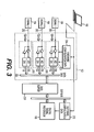
- Figure 3 is a block diagram illustrating the system of Figure 1 in more detail.
- Figure 1 is a representative block diagram illustrating a
system 100 incorporating areconfigurable interface 102. Thereconfigurable interface 102 links devices 104 (e.g., sensors, actuators, loads, etc.) to adigital signal processor 106, which in turn generates an output based on the device information and information in a configuration table 108. Generally, thereconfigurable interface 102 acts as a universal signal conditioner that digitizes outputs having different formats so that they can be processed in thesignal processor 106 without requiring hardware customization of thereconfigurable interface 102 or any other components. Thereconfigurable interface 102 can also convert digital signals into analog signals to be sent back to thedevices 104, if desired. In other words, data in the configuration table 108 configures thereconfigurable interface 102 to be compatible with thedevices 104 so that the device outputs can be converted into a usable format, regardless of the original format of the device output. - The
reconfigurable interface 102 therefore allows thedevices 104 to be changed, removed, and/or added without requiring any hardware reconfiguration to accommodate thenew device 104 configuration. Instead, the configuration table 108 can be modified via any known method (e.g., through auser interface 110 on a computer) to handle the device changes. Also, thereconfigurable interface 102 can be easily expanded and contracted to handle different numbers ofdevices 104 without requiring hardware modifications to thesystem 100. - The configuration table 108 itself include any data that may be used to convert inputs and outputs of the
devices 104 into usable form and to extract intelligence from thedevices 104. For example, the configuration table 108 may include, but is not limited to, pre-processing and post-processing instructions, individual device parameters and ranges, device voltages, filter types, parameters, sampling rates, etc. Inputs can be reconfigured for any sensor within operable limits, and outputs can be reconfigured for any load within operable limits. Moreover, pins on thedevices 104 can be configured as either inputs or outputs, depending on the overall configuration of thesystem 100. The information that could be included in the configuration table 108 is essentially limitless because converting the device outputs into the digital domain without losing any quality of information provides a great deal of flexibility as to how they can be processed and evaluated. For example, if a user wishes to apply a particular filter on a device output, the characteristics of the desired filter can simply be entered into the configuration table 108. This is much more flexible than building an actual customized filter in hardware. - The
reconfigurable interface 102 allows thesame signal processor 106 and general hardware configuration to be used inmultiple systems 100 havingdifferent devices 104. Moreover, eachdevice 104 no longer requires its own unique hardware channel to convert the information from thedevice 104 into digital form to be usable by thesignal processor 106. - As noted above,
different devices 104 may generate outputs having different formats. As is known in the art, input sensors for electrical systems fall in several different categories and output intelligence in different formats. For example, speed and pressure sensors may generate outputs in a frequency signal format, while a potentiometer may generate an output as a DC voltage. Other possible output formats for both sensors and loads include, but are not limited to, variable resistance, AC or DC voltage/current, discrete on/off signals, pulse width modulated signals, and amplitude modulated signals. Those of skill in the art will recognize that the specific format of the output generated by thedevices 104 is not critical to the scope of the invention. - Figure 2 illustrates the operation of the
reconfigurable interface 102 in greater detail. Thedevices 104 and thereconfigurable interface 102 act as ahardware side 140 of thesystem 100. Thereconfigurable interface 102 first receives outputs from thedevices 104 and converts the outputs into digital form immediately in an A/D converter 150, without extracting intelligence from the output. To do this, thereconfigurable interface 102 samples the outputs at a rate fast enough to interpolate the original waveform. The Nyquist Theory states that the sampling frequency needs to be at least twice the absolute maximum frequency that the output can reach to recover all pertinent signal information (i.e., peaks and troughs in the signal). Note that thereconfigurable interface 102 may also include a D/A converter 152 to convert digital signals into an analog format usable by a givendevice 104. The high speeds of currently available A/D converters (for collecting inputs form the devices 104), D/A converters (for controlling output signals) and processors (e.g., thesignal processor 106 and CPUs) allow sampling at rates that satisfy the Nyquist Theory. Thus, it is possible to convert the analog outputs from thedevices 104 into digital form without losing any of the information in the outputs if the outputs are sampled at a rate that is at least the Nyquist sampling rate. - Referring to Figures 2 and 3, each device has an associated reconfigurable input/output hardware channel, each channel having an associated
signal line 202 and aconverter 203 in thereconfigurable interface 102. Theconverter 203 may include the A/D converter 150 and/or the D/A converter 152. Each hardware channel is reconfigurable throughhardware configuration data 204 in the configuration table 108. Theuser interface 110 allows the data in the configuration table 108 to be easily changed so that thesystem 100 can accommodate changes in the number, location, type and output formats of thedevices 104 without requiring any reconfiguration in the hardware. - The
reconfigurable interface 102 then sends the sampled, digitized device output through adata bus 206 into adata buffer 208. Thedata buffer 208 and thesignal processor 106 serve as asoftware side 210 of thesystem 100. Thesignal processor 106 then extracts intelligence from the sampled device outputs based onsoftware configuration data 212 in the configuration table 108. The extracted intelligence may be sent to a target (not shown) for further action. Extracting intelligence from the device output on thesoftware side 210 rather than thehardware side 140 further eliminates the need for any hardware reconfiguration if thedevices 104 change because reconfiguration is conducted through software modifications (i.e., changing data in the configuration table 108) rather than hardware modifications. Because thesignal processor 106 is fast enough to support complex algorithms, it can conduct virtually any desired processing of the device outputs to obtain the needed intelligence from the devices and, if desired, provide thedevices 104 with information in their respective compatible signal formats as well. - As a result, the inventive reconfigurable interface allows the system to be reconfigured to accommodate a variety of sensors having different input/output formats without requiring any hardware modification. Also, the same reconfigurable interface can be used on multiple systems having differing numbers and types of devices without requiring any hardware reconfiguration in the system itself.
- It should be understood that various alternatives to the embodiments of the invention described herein may be employed in practicing the invention. It is intended that the following claims define the scope of the invention and that the method and apparatus within the scope of these claims and their equivalents be covered thereby.
Claims (16)
- A reconfigurable interface (102) for a system, comprising:at least one hardware channel, each hardware channel corresponding with at least one device (104) in the system and having a converter (150,152) and a signal line (202) for connecting the converter to said at least one device, wherein the converter (150,152) converts at least one of an input and an output of said at least one device (104); anda configuration table (108) containing data that configures said at least one hardware channel to be compatible with said at least one device (104).
- The reconfigurable interface of claim 1, wherein the converter comprises an analog-to-digital (A/D) converter (150) that converts an analog output from said at least one device (104) into a digital signal.
- The reconfigurable interface of claim 2, wherein the A/D converter (150) converts the analog output by sampling the analog output at a rate that is at least a Nyquist sampling rate.
- The reconfigurable interface of claim 1, wherein the converter comprises a digital-to-analog (D/A) converter (152) that converts a digital signal into an analog input to said at least one device (104).
- The reconfigurable interface of any preceding claim, wherein said at least one hardware channel comprises a plurality of hardware channels corresponding to a plurality of devices (104).
- The reconfigurable interface of claim 5, wherein said plurality of devices (104) generates outputs having at least two different formats.
- The reconfigurable interface of any preceding claim, further comprising a user interface (110) that communicates with the configuration table (108) to allow modification of the data in the configuration table (108).
- The reconfigurable interface of any preceding claim, wherein the configuration table (108) comprises hardware configuration data that configures said at least one hardware channel and software configuration data that configures a signal processor that processes (106) at least one of the input and the output of said at least one device (104).
- A system, comprising:a plurality of devices (104);a signal processor (106); anda reconfigurable interface (102) coupled between said plurality of devices (104) and the signal processor (106), the reconfigurable interface (102) havingat least one hardware channel, each hardware channel corresponding to one of said plurality of devices (104) and having a converter (150,152) and a signal line (202) connecting the converter (150,152) to the device (104), wherein the converter (150,152) converts at least one of an input and an output of the device (104), anda configuration table (108) containing data that configures said at least one hardware channel to be compatible with said at least one device (104); anda user interface (110) that communicates with the configuration table (108) to allow modification of the data in the configuration table.
- The system of claim 9, further comprising a data buffer (208) in communication with the signal processor (106) and the reconfigurable interface (102), wherein the data buffer (208) stores information from at least one of the reconfigurable interface (102) and the signal processor (106).
- The system of claim 9 or 10, wherein the converter comprises an analog-to-digital (A/D) converter (150) that converts an analog output from said at least one device (104) into a digital signal.
- The system of claim 11, wherein the A/D converter (150) converts the analog output by sampling the analog output at a rate that is at least a Nyquist sampling rate.
- The system of claim 9 or 10, wherein the converter comprises a digital-to-analog (D/A) converter (152) that converts a digital signal into an analog input to said at least one device (104).
- The system of any of claims 9 to 13, wherein said plurality of devices (104) generates outputs having at least two different formats.
- The system of any of claims 9 to 14, wherein the configuration table (108) comprises hardware configuration data that configures the plurality of hardware channels and software configuration data that configures the signal processor (106).
- The system of any of claims 9 to 15, wherein the signal processor (106) extracts intelligence from the output of the device (104) and outputs the intelligence to a target.
Applications Claiming Priority (1)
| Application Number | Priority Date | Filing Date | Title |
|---|---|---|---|
| US11/016,277 US20060136626A1 (en) | 2004-12-17 | 2004-12-17 | Reconfigurable input/output interface |
Publications (3)
| Publication Number | Publication Date |
|---|---|
| EP1672322A2 true EP1672322A2 (en) | 2006-06-21 |
| EP1672322A3 EP1672322A3 (en) | 2009-07-29 |
| EP1672322B1 EP1672322B1 (en) | 2013-01-23 |
Family
ID=36190422
Family Applications (1)
| Application Number | Title | Priority Date | Filing Date |
|---|---|---|---|
| EP05257598A Expired - Lifetime EP1672322B1 (en) | 2004-12-17 | 2005-12-12 | Reconfigurable input/output interface |
Country Status (3)
| Country | Link |
|---|---|
| US (1) | US20060136626A1 (en) |
| EP (1) | EP1672322B1 (en) |
| JP (1) | JP4860999B2 (en) |
Cited By (2)
| Publication number | Priority date | Publication date | Assignee | Title |
|---|---|---|---|---|
| CN102666207A (en) * | 2009-09-29 | 2012-09-12 | 沃尔沃技术公司 | Method and system for preparing sensor output data of a sensor assembly for further processing in at least one application and/or by at least one algorithm |
| US10106171B2 (en) | 2015-07-28 | 2018-10-23 | Crown Equipment Corporation | Vehicle control module with signal switchboard and output tables |
Families Citing this family (4)
| Publication number | Priority date | Publication date | Assignee | Title |
|---|---|---|---|---|
| DE102011106687A1 (en) * | 2011-07-06 | 2013-01-10 | Festo Ag & Co. Kg | Signal processing system and method for processing signals in a bus node |
| US20130262015A1 (en) * | 2012-03-29 | 2013-10-03 | Travis W. L. White | Annotating Measurement Results Data Capture Images with Instrumentation Configuration |
| US20130262016A1 (en) * | 2012-03-29 | 2013-10-03 | Travis W. L. White | Automatically Configuring a Measurement System Using Measurement Results Data Capture Images Annotated with Instrumentation Configuration |
| US10116288B2 (en) | 2017-02-07 | 2018-10-30 | Hamilton Sundstrand Corporation | Reduced overhead on digital signal processing for motor drive applications |
Family Cites Families (15)
| Publication number | Priority date | Publication date | Assignee | Title |
|---|---|---|---|---|
| US4750111A (en) * | 1984-08-22 | 1988-06-07 | Crosby Jr Edward D | Computer system for processing analog and digital data |
| DE69132037T2 (en) * | 1990-09-04 | 2000-11-16 | Motorola, Inc. | Analog-digital conversion system using conversion control words |
| US5168276A (en) * | 1990-09-04 | 1992-12-01 | Motorola, Inc. | Automatic A/D converter operation using a programmable control table |
| US5671355A (en) * | 1992-06-26 | 1997-09-23 | Predacomm, Inc. | Reconfigurable network interface apparatus and method |
| JPH0661698A (en) * | 1992-08-07 | 1994-03-04 | Matsushita Electric Ind Co Ltd | Electronic component mounting machine and computor system therefor |
| JPH06195280A (en) * | 1992-12-22 | 1994-07-15 | Oki Electric Ind Co Ltd | Parameter setting method for serial interface |
| US5628028A (en) * | 1995-03-02 | 1997-05-06 | Data Translation, Inc. | Reprogrammable PCMCIA card and method and apparatus employing same |
| JP2972601B2 (en) * | 1996-10-21 | 1999-11-08 | 日本電気テレコムシステム株式会社 | Wireless communication adapter device |
| US6115654A (en) * | 1997-12-23 | 2000-09-05 | Simmonds Precision Products, Inc. | Universal sensor interface system and method |
| US6362768B1 (en) * | 1999-08-09 | 2002-03-26 | Honeywell International Inc. | Architecture for an input and output device capable of handling various signal characteristics |
| SG118066A1 (en) * | 2000-08-25 | 2006-01-27 | Serial System Ltd | A reconfigurable communication interface and method therefor |
| US6417691B1 (en) * | 2000-08-29 | 2002-07-09 | Motorola, Inc. | Communication device with configurable module interface |
| TW502195B (en) * | 2001-05-11 | 2002-09-11 | Via Tech Inc | Computer system using interface circuit to increase pins of general-purpose input/output port |
| US6839790B2 (en) * | 2002-06-21 | 2005-01-04 | Smar Research Corporation | Plug and play reconfigurable USB interface for industrial fieldbus network access |
| JP2004086492A (en) * | 2002-08-26 | 2004-03-18 | Nec Access Technica Ltd | Assist system for setting connection of peripherals of mobile terminal with camera and its method |
-
2004
- 2004-12-17 US US11/016,277 patent/US20060136626A1/en not_active Abandoned
-
2005
- 2005-12-12 EP EP05257598A patent/EP1672322B1/en not_active Expired - Lifetime
- 2005-12-16 JP JP2005362634A patent/JP4860999B2/en not_active Expired - Fee Related
Non-Patent Citations (1)
| Title |
|---|
| None |
Cited By (4)
| Publication number | Priority date | Publication date | Assignee | Title |
|---|---|---|---|---|
| CN102666207A (en) * | 2009-09-29 | 2012-09-12 | 沃尔沃技术公司 | Method and system for preparing sensor output data of a sensor assembly for further processing in at least one application and/or by at least one algorithm |
| EP2483110A4 (en) * | 2009-09-29 | 2013-05-01 | Volvo Technology Corp | Method and system for preparing sensor output data of a sensor assembly for further processing in at least one application and/or by at least one algorithm |
| US10106171B2 (en) | 2015-07-28 | 2018-10-23 | Crown Equipment Corporation | Vehicle control module with signal switchboard and output tables |
| US10427692B2 (en) | 2015-07-28 | 2019-10-01 | Crown Equipment Corporation | Vehicle control module with signal switchboard and input tables |
Also Published As
| Publication number | Publication date |
|---|---|
| US20060136626A1 (en) | 2006-06-22 |
| JP2006172480A (en) | 2006-06-29 |
| JP4860999B2 (en) | 2012-01-25 |
| EP1672322A3 (en) | 2009-07-29 |
| EP1672322B1 (en) | 2013-01-23 |
Similar Documents
| Publication | Publication Date | Title |
|---|---|---|
| US7340541B2 (en) | Method of buffering bidirectional digital I/O lines | |
| EP1672322B1 (en) | Reconfigurable input/output interface | |
| HARRY LEVITT | Digital hearing aids: A tutorial review | |
| EP3226421A1 (en) | Sensor data processing for condition monitoring systems | |
| DE60001461T2 (en) | ARCHITECTURE FOR AN INPUT / OUTPUT DEVICE FOR TREATING DIFFERENT SIGNAL PROPERTIES | |
| EP3392767A1 (en) | A method for real time processing of fast analogue signals and a system for application thereof | |
| EP2182491B1 (en) | Method to efficiently synchronize multiple measurements across muliple sensor inputs | |
| US4742515A (en) | Data acquistion and control system | |
| WO2005067408A3 (en) | Device, unit and arrangement for one or several distributed systems | |
| Limchesing et al. | Application of EEG Device and BCI for the Brain-controlled Automated Wheelchair | |
| EP3839672B1 (en) | Distributed sensing processing systems | |
| US5034745A (en) | Data acquisition with vernier control | |
| CN219629645U (en) | Electroencephalogram signal acquisition system | |
| CN108287307A (en) | Data processing system for electromechanical testing | |
| US20100070550A1 (en) | Method and apparatus of a sensor amplifier configured for use in medical applications | |
| JP3513633B2 (en) | Method and apparatus for identifying unknown continuous-time system, and control system using the same | |
| CN112486065A (en) | Alternating current signal sampling method and device and handheld code scanning printer | |
| CN109571475B (en) | A force touch control system and robot | |
| JP2769272B2 (en) | Input processing card and output processing card | |
| WO2003105021A2 (en) | Signal processing system and method | |
| JPH06348744A (en) | Data processor | |
| KR20220087759A (en) | Message broker-based data processing and workflow execution system | |
| US6608576B1 (en) | Pulse code modulation encoder for data acquisition | |
| JPH10124443A (en) | Plant control system | |
| JPH07118629B2 (en) | Analog input device with variable filter time constant |
Legal Events
| Date | Code | Title | Description |
|---|---|---|---|
| PUAI | Public reference made under article 153(3) epc to a published international application that has entered the european phase |
Free format text: ORIGINAL CODE: 0009012 |
|
| AK | Designated contracting states |
Kind code of ref document: A2 Designated state(s): AT BE BG CH CY CZ DE DK EE ES FI FR GB GR HU IE IS IT LI LT LU LV MC NL PL PT RO SE SI SK TR |
|
| AX | Request for extension of the european patent |
Extension state: AL BA HR MK YU |
|
| PUAL | Search report despatched |
Free format text: ORIGINAL CODE: 0009013 |
|
| AK | Designated contracting states |
Kind code of ref document: A3 Designated state(s): AT BE BG CH CY CZ DE DK EE ES FI FR GB GR HU IE IS IT LI LT LU LV MC NL PL PT RO SE SI SK TR |
|
| AX | Request for extension of the european patent |
Extension state: AL BA HR MK YU |
|
| 17P | Request for examination filed |
Effective date: 20100127 |
|
| 17Q | First examination report despatched |
Effective date: 20100218 |
|
| AKX | Designation fees paid |
Designated state(s): DE FR GB |
|
| GRAP | Despatch of communication of intention to grant a patent |
Free format text: ORIGINAL CODE: EPIDOSNIGR1 |
|
| GRAS | Grant fee paid |
Free format text: ORIGINAL CODE: EPIDOSNIGR3 |
|
| GRAA | (expected) grant |
Free format text: ORIGINAL CODE: 0009210 |
|
| AK | Designated contracting states |
Kind code of ref document: B1 Designated state(s): DE FR GB |
|
| REG | Reference to a national code |
Ref country code: GB Ref legal event code: FG4D |
|
| REG | Reference to a national code |
Ref country code: DE Ref legal event code: R096 Ref document number: 602005037966 Country of ref document: DE Effective date: 20130321 |
|
| PLBE | No opposition filed within time limit |
Free format text: ORIGINAL CODE: 0009261 |
|
| STAA | Information on the status of an ep patent application or granted ep patent |
Free format text: STATUS: NO OPPOSITION FILED WITHIN TIME LIMIT |
|
| 26N | No opposition filed |
Effective date: 20131024 |
|
| PGFP | Annual fee paid to national office [announced via postgrant information from national office to epo] |
Ref country code: GB Payment date: 20131211 Year of fee payment: 9 |
|
| REG | Reference to a national code |
Ref country code: DE Ref legal event code: R097 Ref document number: 602005037966 Country of ref document: DE Effective date: 20131024 |
|
| REG | Reference to a national code |
Ref country code: DE Ref legal event code: R119 Ref document number: 602005037966 Country of ref document: DE |
|
| REG | Reference to a national code |
Ref country code: DE Ref legal event code: R119 Ref document number: 602005037966 Country of ref document: DE Effective date: 20140701 |
|
| REG | Reference to a national code |
Ref country code: FR Ref legal event code: ST Effective date: 20140829 |
|
| PG25 | Lapsed in a contracting state [announced via postgrant information from national office to epo] |
Ref country code: DE Free format text: LAPSE BECAUSE OF NON-PAYMENT OF DUE FEES Effective date: 20140701 |
|
| PG25 | Lapsed in a contracting state [announced via postgrant information from national office to epo] |
Ref country code: FR Free format text: LAPSE BECAUSE OF NON-PAYMENT OF DUE FEES Effective date: 20131231 |
|
| GBPC | Gb: european patent ceased through non-payment of renewal fee |
Effective date: 20141212 |
|
| PG25 | Lapsed in a contracting state [announced via postgrant information from national office to epo] |
Ref country code: GB Free format text: LAPSE BECAUSE OF NON-PAYMENT OF DUE FEES Effective date: 20141212 |