EP1670061A2 - Semiconductor substrate for solid-state image pickup device and producing method therefor - Google Patents
Semiconductor substrate for solid-state image pickup device and producing method therefor Download PDFInfo
- Publication number
- EP1670061A2 EP1670061A2 EP05026840A EP05026840A EP1670061A2 EP 1670061 A2 EP1670061 A2 EP 1670061A2 EP 05026840 A EP05026840 A EP 05026840A EP 05026840 A EP05026840 A EP 05026840A EP 1670061 A2 EP1670061 A2 EP 1670061A2
- Authority
- EP
- European Patent Office
- Prior art keywords
- semiconductor substrate
- forming
- pixel area
- range
- image pickup
- Prior art date
- Legal status (The legal status is an assumption and is not a legal conclusion. Google has not performed a legal analysis and makes no representation as to the accuracy of the status listed.)
- Withdrawn
Links
Images


Classifications
-
- H—ELECTRICITY
- H10—SEMICONDUCTOR DEVICES; ELECTRIC SOLID-STATE DEVICES NOT OTHERWISE PROVIDED FOR
- H10F—INORGANIC SEMICONDUCTOR DEVICES SENSITIVE TO INFRARED RADIATION, LIGHT, ELECTROMAGNETIC RADIATION OF SHORTER WAVELENGTH OR CORPUSCULAR RADIATION
- H10F39/00—Integrated devices, or assemblies of multiple devices, comprising at least one element covered by group H10F30/00, e.g. radiation detectors comprising photodiode arrays
- H10F39/10—Integrated devices
- H10F39/12—Image sensors
-
- H—ELECTRICITY
- H10—SEMICONDUCTOR DEVICES; ELECTRIC SOLID-STATE DEVICES NOT OTHERWISE PROVIDED FOR
- H10F—INORGANIC SEMICONDUCTOR DEVICES SENSITIVE TO INFRARED RADIATION, LIGHT, ELECTROMAGNETIC RADIATION OF SHORTER WAVELENGTH OR CORPUSCULAR RADIATION
- H10F39/00—Integrated devices, or assemblies of multiple devices, comprising at least one element covered by group H10F30/00, e.g. radiation detectors comprising photodiode arrays
- H10F39/011—Manufacture or treatment of image sensors covered by group H10F39/12
- H10F39/028—Manufacture or treatment of image sensors covered by group H10F39/12 performed after manufacture of the image sensors, e.g. annealing, gettering of impurities, short-circuit elimination or recrystallisation
-
- H—ELECTRICITY
- H10—SEMICONDUCTOR DEVICES; ELECTRIC SOLID-STATE DEVICES NOT OTHERWISE PROVIDED FOR
- H10F—INORGANIC SEMICONDUCTOR DEVICES SENSITIVE TO INFRARED RADIATION, LIGHT, ELECTROMAGNETIC RADIATION OF SHORTER WAVELENGTH OR CORPUSCULAR RADIATION
- H10F71/00—Manufacture or treatment of devices covered by this subclass
- H10F71/121—The active layers comprising only Group IV materials
- H10F71/1221—The active layers comprising only Group IV materials comprising polycrystalline silicon
-
- H—ELECTRICITY
- H10—SEMICONDUCTOR DEVICES; ELECTRIC SOLID-STATE DEVICES NOT OTHERWISE PROVIDED FOR
- H10F—INORGANIC SEMICONDUCTOR DEVICES SENSITIVE TO INFRARED RADIATION, LIGHT, ELECTROMAGNETIC RADIATION OF SHORTER WAVELENGTH OR CORPUSCULAR RADIATION
- H10F77/00—Constructional details of devices covered by this subclass
- H10F77/10—Semiconductor bodies
- H10F77/16—Material structures, e.g. crystalline structures, film structures or crystal plane orientations
- H10F77/162—Non-monocrystalline materials, e.g. semiconductor particles embedded in insulating materials
- H10F77/164—Polycrystalline semiconductors
- H10F77/1642—Polycrystalline semiconductors including only Group IV materials
-
- Y—GENERAL TAGGING OF NEW TECHNOLOGICAL DEVELOPMENTS; GENERAL TAGGING OF CROSS-SECTIONAL TECHNOLOGIES SPANNING OVER SEVERAL SECTIONS OF THE IPC; TECHNICAL SUBJECTS COVERED BY FORMER USPC CROSS-REFERENCE ART COLLECTIONS [XRACs] AND DIGESTS
- Y02—TECHNOLOGIES OR APPLICATIONS FOR MITIGATION OR ADAPTATION AGAINST CLIMATE CHANGE
- Y02P—CLIMATE CHANGE MITIGATION TECHNOLOGIES IN THE PRODUCTION OR PROCESSING OF GOODS
- Y02P70/00—Climate change mitigation technologies in the production process for final industrial or consumer products
- Y02P70/50—Manufacturing or production processes characterised by the final manufactured product
Definitions
- the present invention relates to a gettering substrate for reducing a pixel defect generated by a heavy metal impurity in a solid-state image pickup device such as a CMOS image pickup device, a semiconductor substrate for a solid-state image pickup device, and a producing method therefor.
- a solid-state image pickup device such as a CMOS image pickup device
- a semiconductor substrate for a solid-state image pickup device and a producing method therefor.
- a crystalline defect generated in a photoelectric converting device generates a weak current in a dark state, causing a white dot defect in the image pickup device.
- the IG method is described for example in Japanese Patent Application Laid-open No. H11-021200, and the PBS is described for example in Japanese Patent Application Laid-open No. H07-022429 (corresponding to USP No. 5,419,786).
- Japanese Patent Application Laid-open No. H08-045944 describes a temperature defining prior to a polysilicon film formation on the rear surface
- Japanese Patent Application Laid-open Nos. H08-104592 and H11-103042 describe that an impurity introduction leads to a dark current generation and a white dot defect in the semiconductor image pickup apparatus.
- the IG method and the PBS method are useful.
- Fig. 5 briefly shows an example.
- the PBS method is more effective than the IG method for a certain output, and the IG method is more effective for other output.
- a semiconductor substrate for forming a pixel area provided at a surface thereof with a plurality of pixels for photoelectric conversion including, on a rear surface of the pixel area-bearing surface, a polysilicon film of a thickness T within a range of 0.5 ⁇ T ⁇ 2.0 ⁇ m, and the semiconductor substrate having an oxygen concentration D within a range of 1.3E18 ⁇ D ⁇ 1.5E18 atom/cm 3 (old ASTM).
- the present invention also provides a semiconductor substrate for forming a pixel area provided at a surface thereof with a plurality of pixels for photoelectric conversion, the semiconductor substrate including, on a rear surface of the pixel area-bearing surface, a polysilicon film of a thickness T within a range of 0.5 ⁇ T ⁇ 2.0 ⁇ m, also including a non-defective area in a part of the semiconductor substrate, and having a bulk micro defect density of 1E5/cm 2 or higher in the semiconductor substrate.
- the present invention further provides a producing method for a semiconductor substrate for forming a pixel area provided at a surface thereof with a plurality of pixels for photoelectric conversion, the method including a step of forming a polysilicon film of a thickness T within a range of 0.5 ⁇ T ⁇ 2.0 ⁇ m on a rear surface of the pixel area-bearing surface, and a step of obtaining an oxygen concentration D within a range of 1.3E18 ⁇ D ⁇ 1.5E18 atom/cm 3 (old ASTM) by a thermal process in the semiconductor substrate, and further including a step of executing a thermal process for 1 hour or longer at a temperature H within a range of 450 ⁇ H ⁇ 750°C prior to a step of forming a wiring on the semiconductor substrate.
- the present invention further provides a producing method for a semiconductor substrate for forming a pixel portion provided at a surface thereof with a plurality of pixels for photoelectric conversion, the method including a step of forming a polysilicon film of a thickness T within a range of 0.5 ⁇ T ⁇ 2.0 ⁇ m on a rear surface of the pixel area-bearing surface, a step of forming a non-defective area in a part of the semiconductor substrate, and a step of realizing a bulk micro defect density of 1E5/cm 2 or higher in the semiconductor substrate, and further including a step of executing a thermal process for 1 hour or longer at a temperature H within a range of 450 ⁇ H ⁇ 750°C prior to a step of forming a wiring on the semiconductor substrate.
- the present inventors have noticed a relation between a type of heavy metal inducing a white dot defect in the solid-state image pickup device and an optimum gettering technology for reducing each heavy metal. More specifically, in a configuration having a PBS on a rear surface of the semiconductor substrate opposite to a surface thereof on which a light receiving portion is to be formed, at least either of an oxygen concentration and a BMD in the substrate is controlled in a range so as to reduce a white dot defect to a level substantially not causing a problem in the characteristics of the image pickup device.
- a concentration sufficient for a spontaneous BMD formation in the thermal process is defined as a lower limit, and a concentration for preventing remaining defects is defined as an upper limit.
- Such limit definitions allows the white dot defects to remain within a range not constituting a problem in the solid-state image pickup device.
- a lower limit is so selected as to advantageously capture heavy metals.
- a PBS formation on a semiconductor substrate developed by a CZ method involves a thermal process at 550-650°C, which tends to develop BMD.
- BMD remains on the substrate surface on which a device is to be formed, thereby resulting in drawbacks such as white dot defect.
- the present inventors having found to provide the substrate with a non-defective area (denuded zone) by an IG method prior to PBS formation, also to positively form BMD in the substrate and to thereafter form PBS.
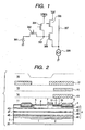
- Fig. 1 is an equivalent circuit diagram of a solid-state image pickup device of the present embodiment.
- CMOS image pickup device having an amplifying element in a light-receiving portion.
- a photodiode (PD) 301 there are provided a photodiode (PD) 301, a transfer MOS transistor 302 for transferring a signal charge generated in the PD, a floating diffusion area (FD) 303 for temporarily storing the transferred signal charge, a resetting MOS transistor 304 for resetting the FD 303, a selecting MOS transistor 305 for selecting an arbitrary row in an array, a source follower MOS transistor 306 for converting the signal charge of the FD 3 into a voltage and amplifying it, a signal readout line 307 for reading a pixel voltage signal commonly for a row, and a constant current source 308.
- PD photodiode
- FD floating diffusion area
- a resetting MOS transistor 304 for resetting the FD 303
- a selecting MOS transistor 305 for selecting an arbitrary row in an array
- a source follower MOS transistor 306 for converting the signal charge of the FD 3 into a voltage and amplifying
- the configuration of a pixel is not limited to the foregoing, and thereby may also be adopted a configuration in which the transfer MOS transistor is omitted, a configuration in which the selecting MOS transistor is omitted, or a configuration sharing a specified MOS transistor for a pixel.
- Fig. 2 is a cross-sectional view of a pixel portion of the present embodiment, illustrating a photodiode portion 1 and a transfer MOS transistor portion 2.
- n-type silicon substrate 3 There are shown an n-type silicon substrate 3, and a P-type well 4 formed by plural layers, having a 4-layered structure with layers 4A-4D in the present embodiment.
- N-type semiconductor layers 4E-4G are provided.
- a gate electrode 7 of the transfer MOS transistor an N-type charge accumulation area 8 of the photodiode, a surface P-type area (constituting a surface charge recombination area) for obtaining PD of an embedded structure, a field oxide film 5 for device isolation, and an N-type high concentration area 10 constituting the FD to which a charge is transferred from the N-type charge accumulation area 8.
- a silicon oxide film 11 for insulating the gate electrode and a first metal layer a contact plug 12, a first metal layer 13, an interlayer insulation film 14 for insulating the first metal layer and a second metal layer, a second metal layer 15, an interlayer insulation film 16 for insulating the second metal layer and a third metal layer, a third metal layer 17, and a passivation film 18.
- the passivation film 18 On the passivation film 18, there are formed a color filter layer and a microlens for sensitivity increase, which are not illustrated.
- the wiring layer has a three-layered structure, but the wiring layer of one- or two-layered structure, for securing the optical characteristics according the specification of the sensor, is not against the principle of the present invention.
- a reduction of the white dot defect in the semiconductor image pickup apparatus can be achieved by a metal gettering on a gettering site to induce a redistribution of a metal impurity in the direction of depth, thereby eliminating the metal from the N-type charge accumulation area 8 of the depleted PD.
- n-substrate (100) is prepared.
- a polysilicon 20 constituting PBS is formed on the rear surface of the substrate, and, as BMD is spontaneously formed by a thermal processing in the process, the oxygen concentration D in the substrate is made 1.3E18 atom/cm 3 (old ASTM) or higher, and is made 1.5E18 atom/cm 3 (old ASTM) or lower in order to prevent residual defects.
- a value of 1.4E18 atom/cm 3 (old ASTM) or higher allows to bring the BMD density to a more preferred range.
- Conditions of thermal processing may be so selected as to obtain an oxygen concentration as described above.
- the polysilicon 20 preferably has a film thickness T of 0.5 ⁇ m or more for obtaining a gettering effect, and 2.0 ⁇ m or less in consideration of productivity.
- the old ASTM means old standards of the American Society for Testing and Materials.
- a field oxide film 5 is formed on the silicon substrate 3 by an ordinary LOCOS method or a recessed LOCOS method.
- a plural-layered P-well is formed by executing ion plantations of four times in the present embodiment with a P-type impurity (such as boron) in succession from the deepest layer with a high energy ion implantation apparatus, and by not executing a high-temperature thermal process such as drive-in thereafter.
- a P-type impurity such as boron
- the thermal process executed thereafter is at about 950°C at maximum.
- an N-type charge accumulation area 8 of the photodiode, a P-surface layer 9 and an N-type high concentration layer 10 are formed by ion implantation.
- a PBS formation on a rear surface of the substrate opposite to the pixel area-bearing surface and a defining of the oxygen concentration in the substrate as in the present embodiment allow to reduce the white dot defects in comparison with a substrate not subjected to such gettering process.
- the present embodiment is different from the first embodiment in that, in order to further increase BMD by a thermal processing in the production process, a low-temperature thermal process at a temperature H within a range of 450 to 750°C for 1 hour or longer is added prior to a step of forming a wiring.
- the present embodiment is different from the first embodiment in that an IG process is applied to the PBS substrate thereby positively forming BMD in the substrate.
- the substrate producing process of the present embodiment will be explained with reference to Figs. 3A-3F.
- n-type (100) silicon substrate 501 obtained by a CZ (Czochralki) process is prepared (Fig. 3A).
- An oxygen concentration in the substrate is preferably 1.4E18 atom/cm 3 or higher in order to increase the BMD density.
- Such substrate 501 is subjected to a mirror polishing on the top surface or on the top and rear surfaces, and is then subjected to a high-temperature thermal process at 1100°C or higher to externally diffuse oxygen on the substrate surface, thereby forming a denuded zone (DZ) 502 constituting a defect-free area on the substrate surface on which a device is to be formed (Fig. 3B).
- DZ denuded zone
- a low-temperature thermal process is executed at about 550-650°C to form oxygen precipitation nuclei in the substrate, and a thermal process is executed at 900°C or higher to form BMD by such oxygen precipitation nuclei (Fig. 3C).
- an epitaxial layer may be or may not be formed, and there is not change in the gettering effect to be obtained.
- the substrate surfaces are oxidized by several tens of nanometers in an oxygen atmosphere (Fig. 3C), thereby forming silicon oxide films 504 on the top and rear surfaces.
- Such polysilicon layer is to constitute PBS, and preferably has a thickness of 0.5 ⁇ m or more in order to obtain a gettering effect and 2.0 ⁇ m or less in consideration of the productivity.
- the white dot defects can be further reduced by adding a low-temperature thermal process at 450-750°C for 1 hour or longer prior to the step of forming a wiring.
- Fig. 4 is a chart showing experimental results of the foregoing embodiments and comparative examples.
- DZ-IG indicates an example in which DZ alone is formed by the IG method
- PBS low oxygen concentration
- the first embodiment of the present invention has a PBS and specifies the oxygen concentration in the substrate (high oxygen concentration).
- the second embodiment utilizes a low-temperature process for example in a wiring step (PBS (high oxygen concentration & low-temperature process)).
- the third embodiment has a PBS and a DZ formed on the substrate top surface by IG method (PBS & DZ-IG), or further has a low-temperature thermal process (PBS & DZ-IG (low-temperature process)). These embodiments of the invention are capable of reducing the white dot defects.
- the case “PBS (high oxygen concentration)” showed defects reduced by about 10 % in comparison with the case “DZ-IG", and the case “PBS (high oxygen concentration & low-temperature process)” showed defects reduced by about 20 % in comparison with the case “DZ-IG”. Further, the case “PBS & DZ-IG” showed defects reduced by about 40 % in comparison with the case “DZ-IG”, and the case “PBS & DZ-IG (low-temperature process)” showed defects reduced by about 20 % in comparison with the case "DZ-IG".
- a semiconductor substrate for forming a pixel area provided surfacially with a plurality of pixels for photoelectric conversion including a polysilicon film of a thickness of 0.5-2.0, on a rear surface of the pixel area-bearing surface, and having an oxygen concentration of 1.3-1.5E+18 atom/cm 3 (old ASTM).
Landscapes
- Solid State Image Pick-Up Elements (AREA)
Abstract
Description
- The present invention relates to a gettering substrate for reducing a pixel defect generated by a heavy metal impurity in a solid-state image pickup device such as a CMOS image pickup device, a semiconductor substrate for a solid-state image pickup device, and a producing method therefor. Related Background Art
- It is already known that, in a semiconductor device manufacturing process, characteristics of the device are deteriorated when a crystalline defect, generated by a contamination by a heavy metal such as Fe, Ni, Cr etc. present in a semiconductor substrate, is formed on a surface of the semiconductor substrate on which a device is to be formed.
- In particular, in a CMS image pickup device, a crystalline defect generated in a photoelectric converting device generates a weak current in a dark state, causing a white dot defect in the image pickup device.
- For reducing such white dot defect, there has been employed an IG (intrinsic gettering) method or a PBS (polysilicon back seal) method.
- The IG method is described for example in Japanese Patent Application Laid-open No. H11-021200, and the PBS is described for example in Japanese Patent Application Laid-open No. H07-022429 (corresponding to USP No. 5,419,786).
- Also in order to avoid a drawback of excessive BMD (bulk micro defect) generation in the PBS method, Japanese Patent Application Laid-open No. H08-045944 describes a temperature defining prior to a polysilicon film formation on the rear surface, and Japanese Patent Application Laid-open Nos. H08-104592 and H11-103042 describe that an impurity introduction leads to a dark current generation and a white dot defect in the semiconductor image pickup apparatus.
- It is also known that an output of the white dot defect in the image pickup apparatus depends on a type of heavy metal constituting the cause thereof.
- For gettering of such various heavy metals, the IG method and the PBS method are useful.
- However, a single gettering technology is insufficient for achieving a gettering effect for plural heavy metals.
- This is because each heavy metal has a matching gettering technology. Fig. 5 briefly shows an example.
- It is shown that the PBS method is more effective than the IG method for a certain output, and the IG method is more effective for other output.
- Therefore, for reducing the number of white dot defects thereby improving the image obtained by the image pickup apparatus, there is desired a gettering technology effective for various heavy metals constituting the cause of such defects.
- The above-mentioned objective can be attained, according to the present invention, by a semiconductor substrate for forming a pixel area provided at a surface thereof with a plurality of pixels for photoelectric conversion, the semiconductor substrate including, on a rear surface of the pixel area-bearing surface, a polysilicon film of a thickness T within a range of 0.5 ≤ T ≤ 2.0 µm, and the semiconductor substrate having an oxygen concentration D within a range of 1.3E18 ≤ D ≤ 1.5E18 atom/cm3 (old ASTM).
- The present invention also provides a semiconductor substrate for forming a pixel area provided at a surface thereof with a plurality of pixels for photoelectric conversion, the semiconductor substrate including, on a rear surface of the pixel area-bearing surface, a polysilicon film of a thickness T within a range of 0.5 ≤ T ≤ 2.0 µm, also including a non-defective area in a part of the semiconductor substrate, and having a bulk micro defect density of 1E5/cm2 or higher in the semiconductor substrate.
- The present invention further provides a producing method for a semiconductor substrate for forming a pixel area provided at a surface thereof with a plurality of pixels for photoelectric conversion, the method including a step of forming a polysilicon film of a thickness T within a range of 0.5 ≤ T ≤ 2.0 µm on a rear surface of the pixel area-bearing surface, and a step of obtaining an oxygen concentration D within a range of 1.3E18 ≤ D ≤ 1.5E18 atom/cm3 (old ASTM) by a thermal process in the semiconductor substrate, and further including a step of executing a thermal process for 1 hour or longer at a temperature H within a range of 450 ≤ H ≤ 750°C prior to a step of forming a wiring on the semiconductor substrate.
- The present invention further provides a producing method for a semiconductor substrate for forming a pixel portion provided at a surface thereof with a plurality of pixels for photoelectric conversion, the method including a step of forming a polysilicon film of a thickness T within a range of 0.5 ≤ T ≤ 2.0 µm on a rear surface of the pixel area-bearing surface, a step of forming a non-defective area in a part of the semiconductor substrate, and a step of realizing a bulk micro defect density of 1E5/cm2 or higher in the semiconductor substrate, and further including a step of executing a thermal process for 1 hour or longer at a temperature H within a range of 450 ≤ H ≤ 750°C prior to a step of forming a wiring on the semiconductor substrate.
- Other features and advantages of the present invention will become apparent from the following description taken in conjunction with the accompanying drawings, in which like reference characters designate the same or similar parts throughout the figures thereof.
-
- Fig. 1 is an equivalent circuit diagram of a semiconductor image pickup apparatus in a first embodiment of the present invention;
- Fig. 2 is a cross sectional view of a pixel portion in the first embodiment of the present invention;
- Figs. 3A, 3B, 3C, 3D, 3E and 3F are cross sectional views showing a substrate preparation process in a third embodiment of the present invention;
- Fig. 4 is a chart showing experimental results on white dot defects in embodiments of the present invention and comparative examples; and
- Fig. 5 is a chart showing an effect of a gettering technology.
- The accompanying drawings, which are incorporated in and constitutes a part of the specification, illustrate embodiments of the invention and, together with the description, serve to explain the principles of the invention.
- The present inventors have noticed a relation between a type of heavy metal inducing a white dot defect in the solid-state image pickup device and an optimum gettering technology for reducing each heavy metal. More specifically, in a configuration having a PBS on a rear surface of the semiconductor substrate opposite to a surface thereof on which a light receiving portion is to be formed, at least either of an oxygen concentration and a BMD in the substrate is controlled in a range so as to reduce a white dot defect to a level substantially not causing a problem in the characteristics of the image pickup device.
- For the oxygen concentration in the semiconductor substrate with PBS, a concentration sufficient for a spontaneous BMD formation in the thermal process is defined as a lower limit, and a concentration for preventing remaining defects is defined as an upper limit.
- Such limit definitions allows the white dot defects to remain within a range not constituting a problem in the solid-state image pickup device.
- Also for the BMD density in the semiconductor substrate with PBS, a lower limit is so selected as to advantageously capture heavy metals.
- Preparation of a substrate equipped with such two gettering layers can be realized as follows.
- A PBS formation on a semiconductor substrate developed by a CZ method involves a thermal process at 550-650°C, which tends to develop BMD.
- Thus BMD remains on the substrate surface on which a device is to be formed, thereby resulting in drawbacks such as white dot defect.
- For avoiding such drawbacks, it is commonly executed to lower the oxygen concentration in the substrate, constituting the cause for BMD, or to apply an appropriate thermal process prior to the PBS formation thereby setting BMD in the substrate at 1E+5/cm2 or less even in a PBS substrate.
- In contrast, the present inventors having found to provide the substrate with a non-defective area (denuded zone) by an IG method prior to PBS formation, also to positively form BMD in the substrate and to thereafter form PBS.
- In this manner there can be realized preparation of a semiconductor substrate in which surface defects do not remain by the PBS and which effectively reduces the white dot damage in the image pickup device.
- Also it is furthermore effective, as described in the foregoing, to apply, to such substrate, a final low-temperature thermal processing at 450-750°C for 1 hour or longer prior to a step of forming a wiring.
- In the following, the present invention will be clarified further by embodiments thereof.
- Fig. 1 is an equivalent circuit diagram of a solid-state image pickup device of the present embodiment.
- The present embodiment will be explained by so-called CMOS image pickup device having an amplifying element in a light-receiving portion.
- There are provided a photodiode (PD) 301, a
transfer MOS transistor 302 for transferring a signal charge generated in the PD, a floating diffusion area (FD) 303 for temporarily storing the transferred signal charge, a resettingMOS transistor 304 for resetting theFD 303, a selectingMOS transistor 305 for selecting an arbitrary row in an array, a sourcefollower MOS transistor 306 for converting the signal charge of theFD 3 into a voltage and amplifying it, asignal readout line 307 for reading a pixel voltage signal commonly for a row, and a constantcurrent source 308. - However the configuration of a pixel is not limited to the foregoing, and thereby may also be adopted a configuration in which the transfer MOS transistor is omitted, a configuration in which the selecting MOS transistor is omitted, or a configuration sharing a specified MOS transistor for a pixel.
- Fig. 2 is a cross-sectional view of a pixel portion of the present embodiment, illustrating a
photodiode portion 1 and a transferMOS transistor portion 2. - There are shown an n-
type silicon substrate 3, and a P-type well 4 formed by plural layers, having a 4-layered structure withlayers 4A-4D in the present embodiment. - Between the
layers 4A-4D of the well, N-type semiconductor layers 4E-4G are provided. - There are also shown a
gate electrode 7 of the transfer MOS transistor, an N-typecharge accumulation area 8 of the photodiode, a surface P-type area (constituting a surface charge recombination area) for obtaining PD of an embedded structure, afield oxide film 5 for device isolation, and an N-typehigh concentration area 10 constituting the FD to which a charge is transferred from the N-typecharge accumulation area 8. - There are further shown a
silicon oxide film 11 for insulating the gate electrode and a first metal layer, acontact plug 12, afirst metal layer 13, aninterlayer insulation film 14 for insulating the first metal layer and a second metal layer, asecond metal layer 15, aninterlayer insulation film 16 for insulating the second metal layer and a third metal layer, athird metal layer 17, and apassivation film 18. - On the
passivation film 18, there are formed a color filter layer and a microlens for sensitivity increase, which are not illustrated. - In the present embodiment, the wiring layer has a three-layered structure, but the wiring layer of one- or two-layered structure, for securing the optical characteristics according the specification of the sensor, is not against the principle of the present invention.
- A reduction of the white dot defect in the semiconductor image pickup apparatus can be achieved by a metal gettering on a gettering site to induce a redistribution of a metal impurity in the direction of depth, thereby eliminating the metal from the N-type
charge accumulation area 8 of the depleted PD. - In the following, a producing process will be explained with reference to a cross-sectional view shown in Fig. 2.
- At first an n-substrate (100) is prepared.
- A
polysilicon 20 constituting PBS is formed on the rear surface of the substrate, and, as BMD is spontaneously formed by a thermal processing in the process, the oxygen concentration D in the substrate is made 1.3E18 atom/cm3 (old ASTM) or higher, and is made 1.5E18 atom/cm3 (old ASTM) or lower in order to prevent residual defects. - More preferably, a value of 1.4E18 atom/cm3 (old ASTM) or higher allows to bring the BMD density to a more preferred range.
- Conditions of thermal processing may be so selected as to obtain an oxygen concentration as described above.
- The
polysilicon 20 preferably has a film thickness T of 0.5 µm or more for obtaining a gettering effect, and 2.0 µm or less in consideration of productivity. - The old ASTM means old standards of the American Society for Testing and Materials.
- Then a
field oxide film 5 is formed on thesilicon substrate 3 by an ordinary LOCOS method or a recessed LOCOS method. - After a
channel stop layer 6 is formed under thefield oxide film 5, a plural-layered P-well is formed by executing ion plantations of four times in the present embodiment with a P-type impurity (such as boron) in succession from the deepest layer with a high energy ion implantation apparatus, and by not executing a high-temperature thermal process such as drive-in thereafter. - The thermal process executed thereafter is at about 950°C at maximum.
- Then, after formation of a
polysilicon electrode 7, an N-typecharge accumulation area 8 of the photodiode, a P-surface layer 9 and an N-typehigh concentration layer 10 are formed by ion implantation. - The producing process after a contact hole opening step is same as that in a prior CMOS area sensor and will not, therefore, be explained further.
- A PBS formation on a rear surface of the substrate opposite to the pixel area-bearing surface and a defining of the oxygen concentration in the substrate as in the present embodiment allow to reduce the white dot defects in comparison with a substrate not subjected to such gettering process.
- The present embodiment is different from the first embodiment in that, in order to further increase BMD by a thermal processing in the production process, a low-temperature thermal process at a temperature H within a range of 450 to 750°C for 1 hour or longer is added prior to a step of forming a wiring.
- Other conditions are same as in the first embodiment.
- The present embodiment is different from the first embodiment in that an IG process is applied to the PBS substrate thereby positively forming BMD in the substrate. The substrate producing process of the present embodiment will be explained with reference to Figs. 3A-3F.
- At first an n-type (100) silicon substrate 501 obtained by a CZ (Czochralki) process is prepared (Fig. 3A).
- An oxygen concentration in the substrate is preferably 1.4E18 atom/cm3 or higher in order to increase the BMD density.
- Such substrate 501 is subjected to a mirror polishing on the top surface or on the top and rear surfaces, and is then subjected to a high-temperature thermal process at 1100°C or higher to externally diffuse oxygen on the substrate surface, thereby forming a denuded zone (DZ) 502 constituting a defect-free area on the substrate surface on which a device is to be formed (Fig. 3B).
- Then a low-temperature thermal process is executed at about 550-650°C to form oxygen precipitation nuclei in the substrate, and a thermal process is executed at 900°C or higher to form BMD by such oxygen precipitation nuclei (Fig. 3C).
- Thereafter an epitaxial layer may be or may not be formed, and there is not change in the gettering effect to be obtained.
- Then the substrate surfaces are oxidized by several tens of nanometers in an oxygen atmosphere (Fig. 3C), thereby forming
silicon oxide films 504 on the top and rear surfaces. - Thereafter, the
silicon oxide film 504 on the rear surface is etched off (Fig. 3D), and a polysilicon layers 505 are formed (Fig. 3E). - Such polysilicon layer is to constitute PBS, and preferably has a thickness of 0.5 µm or more in order to obtain a gettering effect and 2.0 µm or less in consideration of the productivity.
- Then the
polysilicon layer 505 and thesilicon oxide film 504 on the top surface are etched off, thereby obtaining two gettering layers of IG and PBS (Fig. 3F). - The process conditions thereafter are same as in the first and second embodiments.
- As explained in the second embodiment, the white dot defects can be further reduced by adding a low-temperature thermal process at 450-750°C for 1 hour or longer prior to the step of forming a wiring.
- Fig. 4 is a chart showing experimental results of the foregoing embodiments and comparative examples.
- In Fig. 4, DZ-IG indicates an example in which DZ alone is formed by the IG method, and PBS (low oxygen concentration) indicates an example in which PBS is formed on the rear surface of the pixel area-bearing surface, but the oxygen concentration is lower than that specified in the first embodiment. These two constitute comparative examples.
- On the other hand, the first embodiment of the present invention has a PBS and specifies the oxygen concentration in the substrate (high oxygen concentration). The second embodiment utilizes a low-temperature process for example in a wiring step (PBS (high oxygen concentration & low-temperature process)). The third embodiment has a PBS and a DZ formed on the substrate top surface by IG method (PBS & DZ-IG), or further has a low-temperature thermal process (PBS & DZ-IG (low-temperature process)). These embodiments of the invention are capable of reducing the white dot defects.
- More specifically, the case "PBS (high oxygen concentration)" showed defects reduced by about 10 % in comparison with the case "DZ-IG", and the case "PBS (high oxygen concentration & low-temperature process)" showed defects reduced by about 20 % in comparison with the case "DZ-IG". Further, the case "PBS & DZ-IG" showed defects reduced by about 40 % in comparison with the case "DZ-IG", and the case "PBS & DZ-IG (low-temperature process)" showed defects reduced by about 20 % in comparison with the case "DZ-IG".
- A semiconductor substrate for forming a pixel area provided surfacially with a plurality of pixels for photoelectric conversion, the semiconductor substrate, including a polysilicon film of a thickness of 0.5-2.0, on a rear surface of the pixel area-bearing surface, and having an oxygen concentration of 1.3-1.5E+18 atom/cm3 (old ASTM).
Claims (6)
- A semiconductor substrate for forming a pixel area provided at a surface thereof with a plurality of pixels for photoelectric conversion, the semiconductor substrate comprising:a polysilicon film of a thickness T within a range of 0.5 ≤ T ≤ 2.0 µm, on a rear surface of the pixel area-bearing surface;wherein the semiconductor substrate has an oxygen concentration D within a range of 1.3E18 ≤ D ≤ 1.5E18 atom/cm3 (old ASTM).
- A semiconductor substrate for forming a pixel area provided at a surface thereof with a plurality of pixels for photoelectric conversion, the semiconductor substrate comprising:a polysilicon film of a thickness T within a range of 0.5 ≤ T ≤ 2.0 µm, on a rear surface of the pixel area-bearing surface: anda non-defective area formed in a part of the semiconductor substrate:wherein the semiconductor substrate has a bulk micro defect density of 1E5/cm2 or higher.
- A solid-state image pickup device comprising a semiconductor substrate according to claim 1.
- A semiconductor image pickup device comprising a semiconductor substrate according to claim 2.
- A producing method for a semiconductor substrate for forming a pixel area provided surfacially with a plurality of pixels for photoelectric conversion, the method comprising:a step of forming a polysilicon film of a thickness T within a range of 0.5 ≤ T ≤ 2.0 µm on a rear surface of the pixel area-bearing surface; anda step of obtaining an oxygen concentration D within a range of 1.3E18 ≤ D ≤ 1.5E18 atom/cm3 (old ASTM) by a thermal process in the semiconductor substrate; and further comprisinga step of executing a thermal process for 1 hour or longer at a temperature H within a range of 450 ≤ H ≤ 750°C prior to a step of forming a wiring on the semiconductor substrate.
- A producing method for a semiconductor substrate for forming a pixel area provided surfacially with a plurality of pixels for photoelectric conversion, the method comprising:a step of forming a polysilicon film of a thickness T within a range of 0.5 ≤ T ≤ 2.0 µm on a rear surface of the pixel area-bearing surface;a step of forming a non-defective area in a part of the semiconductor substrate; anda step of realizing a bulk micro defect density of 1E5/cm2 or higher in the semiconductor substrate by a thermal process;and further comprising;a step of executing a thermal process for 1 hour or longer at a temperature H within a range of 450 ≤ H ≤ 750°C prior to a step of forming a wiring on the semiconductor substrate.
Applications Claiming Priority (1)
| Application Number | Priority Date | Filing Date | Title |
|---|---|---|---|
| JP2004358343A JP4667030B2 (en) | 2004-12-10 | 2004-12-10 | Semiconductor substrate for solid-state imaging device and manufacturing method thereof |
Publications (2)
| Publication Number | Publication Date |
|---|---|
| EP1670061A2 true EP1670061A2 (en) | 2006-06-14 |
| EP1670061A3 EP1670061A3 (en) | 2011-05-04 |
Family
ID=35583558
Family Applications (1)
| Application Number | Title | Priority Date | Filing Date |
|---|---|---|---|
| EP05026840A Withdrawn EP1670061A3 (en) | 2004-12-10 | 2005-12-08 | Semiconductor substrate for solid-state image pickup device and producing method therefor |
Country Status (3)
| Country | Link |
|---|---|
| US (1) | US7387952B2 (en) |
| EP (1) | EP1670061A3 (en) |
| JP (1) | JP4667030B2 (en) |
Families Citing this family (3)
| Publication number | Priority date | Publication date | Assignee | Title |
|---|---|---|---|---|
| JP5825931B2 (en) * | 2011-08-25 | 2015-12-02 | グローバルウェーハズ・ジャパン株式会社 | Manufacturing method of solid-state imaging device |
| JP6861471B2 (en) * | 2015-06-12 | 2021-04-21 | キヤノン株式会社 | Imaging device and its manufacturing method and camera |
| JP6862129B2 (en) * | 2016-08-29 | 2021-04-21 | キヤノン株式会社 | Photoelectric converter and imaging system |
Family Cites Families (27)
| Publication number | Priority date | Publication date | Assignee | Title |
|---|---|---|---|---|
| JPS5680139A (en) * | 1979-12-05 | 1981-07-01 | Chiyou Lsi Gijutsu Kenkyu Kumiai | Manufacture of semiconductor device |
| US4608095A (en) * | 1983-02-14 | 1986-08-26 | Monsanto Company | Gettering |
| US4851358A (en) * | 1988-02-11 | 1989-07-25 | Dns Electronic Materials, Inc. | Semiconductor wafer fabrication with improved control of internal gettering sites using rapid thermal annealing |
| ATE155928T1 (en) | 1990-05-31 | 1997-08-15 | Canon Kk | METHOD FOR PRODUCING A SEMICONDUCTOR MEMORY ARRANGEMENT WITH A CAPACITOR |
| JPH0453140A (en) * | 1990-06-18 | 1992-02-20 | Fujitsu Ltd | Processing of silicon single crystalline wafer |
| JP3011982B2 (en) * | 1990-09-14 | 2000-02-21 | コマツ電子金属株式会社 | Method for manufacturing semiconductor device |
| JP2765635B2 (en) * | 1991-01-11 | 1998-06-18 | キヤノン株式会社 | Photoelectric conversion device |
| JPH04262537A (en) * | 1991-02-15 | 1992-09-17 | Canon Inc | Manufacturing method of photoelectric conversion device |
| JP2726583B2 (en) * | 1991-11-18 | 1998-03-11 | 三菱マテリアルシリコン株式会社 | Semiconductor substrate |
| US5534069A (en) * | 1992-07-23 | 1996-07-09 | Canon Kabushiki Kaisha | Method of treating active material |
| JP3232168B2 (en) * | 1993-07-02 | 2001-11-26 | 三菱電機株式会社 | Semiconductor substrate, method of manufacturing the same, and semiconductor device using the semiconductor substrate |
| JP3524141B2 (en) * | 1994-03-25 | 2004-05-10 | 株式会社東芝 | Semiconductor device and manufacturing method thereof |
| JPH0845944A (en) | 1994-07-29 | 1996-02-16 | Sumitomo Sitix Corp | Silicon wafer manufacturing method |
| JPH08104592A (en) | 1994-08-09 | 1996-04-23 | Sony Corp | Method for manufacturing semiconductor substrate for semiconductor device and semiconductor device |
| JP3171308B2 (en) * | 1995-06-28 | 2001-05-28 | 東芝セラミックス株式会社 | Silicon wafer and method for manufacturing the same |
| US6541454B1 (en) * | 1995-04-04 | 2003-04-01 | Yissum Research Development Company Of The Hebrew University Jerusalem | Phosphonates, biphosphonates and pharmaceutical compositions containing them |
| JPH10270455A (en) * | 1997-03-26 | 1998-10-09 | Toshiba Corp | Semiconductor substrate manufacturing method |
| JP3944958B2 (en) | 1997-07-02 | 2007-07-18 | 株式会社Sumco | Silicon epitaxial wafer and manufacturing method thereof |
| TW429478B (en) * | 1997-08-29 | 2001-04-11 | Toshiba Corp | Semiconductor device and method for manufacturing the same |
| JPH11103042A (en) | 1997-09-26 | 1999-04-13 | Sony Corp | Semiconductor substrate for solid-state imaging device and method of manufacturing solid-state imaging device |
| EP1087041B1 (en) * | 1999-03-16 | 2009-01-07 | Shin-Etsu Handotai Co., Ltd | Production method for silicon wafer and silicon wafer |
| JP2001237247A (en) * | 2000-02-25 | 2001-08-31 | Shin Etsu Handotai Co Ltd | Method of manufacturing epitaxial wafer, epitaxial wafer and cz silicon wafer for epitaxial growth |
| WO2001082382A1 (en) * | 2000-04-20 | 2001-11-01 | Digirad Corporation | Fabrication of low leakage-current backside illuminated photodiodes |
| US7081422B2 (en) * | 2000-12-13 | 2006-07-25 | Shin-Etsu Handotai Co., Ltd. | Manufacturing process for annealed wafer and annealed wafer |
| KR100423752B1 (en) * | 2001-11-12 | 2004-03-22 | 주식회사 실트론 | A Semiconductor Silicon Wafer and a Method for making thereof |
| JP4288406B2 (en) * | 2003-01-17 | 2009-07-01 | 株式会社ニコン | Method for manufacturing solid-state imaging device |
| JP4510414B2 (en) * | 2003-09-12 | 2010-07-21 | キヤノン株式会社 | Photoelectric conversion device |
-
2004
- 2004-12-10 JP JP2004358343A patent/JP4667030B2/en not_active Expired - Fee Related
-
2005
- 2005-12-02 US US11/291,955 patent/US7387952B2/en not_active Expired - Fee Related
- 2005-12-08 EP EP05026840A patent/EP1670061A3/en not_active Withdrawn
Also Published As
| Publication number | Publication date |
|---|---|
| US20060124929A1 (en) | 2006-06-15 |
| JP4667030B2 (en) | 2011-04-06 |
| US7387952B2 (en) | 2008-06-17 |
| EP1670061A3 (en) | 2011-05-04 |
| JP2006165462A (en) | 2006-06-22 |
Similar Documents
| Publication | Publication Date | Title |
|---|---|---|
| US7952096B2 (en) | CMOS image sensor with improved backside surface treatment | |
| US8741681B2 (en) | Solid-state image pickup device and method for producing the same | |
| US7843027B2 (en) | Solid-state imaging device, camera and method of producing the solid-state imaging device | |
| CN102362351B (en) | Back-illuminated cmos image sensors | |
| EP0503666B1 (en) | CCD solid state image sensing device | |
| US8614112B2 (en) | Method of damage-free impurity doping for CMOS image sensors | |
| US7994552B2 (en) | Photoelectric conversion device, method for manufacturing the same and image pickup system | |
| TW201027737A (en) | Technique for fabrication of backside illuminated image sensor | |
| CN104637966A (en) | Semiconductor device and method of manufacturing same | |
| US7589366B2 (en) | Solid-state imaging device and method for manufacturing the same | |
| US5288656A (en) | Method of manufacturing a CCD solid state image sensing device | |
| US7387952B2 (en) | Semiconductor substrate for solid-state image pickup device and producing method therefor | |
| CN100423278C (en) | CMOS image sensor and manufacturing method thereof | |
| JP2004047985A (en) | Solid-state imaging device | |
| US20060019423A1 (en) | Method for manufacturing solid-state image sensor | |
| JPH04171762A (en) | Solid-stage image sensing device and manufacture thereof | |
| JP2004079657A (en) | Method for manufacturing solid-state imaging device |
Legal Events
| Date | Code | Title | Description |
|---|---|---|---|
| PUAI | Public reference made under article 153(3) epc to a published international application that has entered the european phase |
Free format text: ORIGINAL CODE: 0009012 |
|
| AK | Designated contracting states |
Kind code of ref document: A2 Designated state(s): AT BE BG CH CY CZ DE DK EE ES FI FR GB GR HU IE IS IT LI LT LU LV MC NL PL PT RO SE SI SK TR |
|
| AX | Request for extension of the european patent |
Extension state: AL BA HR MK YU |
|
| PUAL | Search report despatched |
Free format text: ORIGINAL CODE: 0009013 |
|
| AK | Designated contracting states |
Kind code of ref document: A3 Designated state(s): AT BE BG CH CY CZ DE DK EE ES FI FR GB GR HU IE IS IT LI LT LU LV MC NL PL PT RO SE SI SK TR |
|
| AX | Request for extension of the european patent |
Extension state: AL BA HR MK YU |
|
| STAA | Information on the status of an ep patent application or granted ep patent |
Free format text: STATUS: THE APPLICATION HAS BEEN WITHDRAWN |
|
| 18W | Application withdrawn |
Effective date: 20110803 |