EP1670013A2 - Electrical switching apparatus including a housing and a trip circuit forming a composite structure - Google Patents
Electrical switching apparatus including a housing and a trip circuit forming a composite structure Download PDFInfo
- Publication number
- EP1670013A2 EP1670013A2 EP05026827A EP05026827A EP1670013A2 EP 1670013 A2 EP1670013 A2 EP 1670013A2 EP 05026827 A EP05026827 A EP 05026827A EP 05026827 A EP05026827 A EP 05026827A EP 1670013 A2 EP1670013 A2 EP 1670013A2
- Authority
- EP
- European Patent Office
- Prior art keywords
- printed circuit
- housing
- operating mechanism
- separable contacts
- circuit board
- Prior art date
- Legal status (The legal status is an assumption and is not a legal conclusion. Google has not performed a legal analysis and makes no representation as to the accuracy of the status listed.)
- Granted
Links
Images





Classifications
-
- H—ELECTRICITY
- H01—ELECTRIC ELEMENTS
- H01H—ELECTRIC SWITCHES; RELAYS; SELECTORS; EMERGENCY PROTECTIVE DEVICES
- H01H71/00—Details of the protective switches or relays covered by groups H01H73/00 - H01H83/00
- H01H71/10—Operating or release mechanisms
- H01H71/12—Automatic release mechanisms with or without manual release
- H01H71/123—Automatic release mechanisms with or without manual release using a solid-state trip unit
-
- H—ELECTRICITY
- H01—ELECTRIC ELEMENTS
- H01H—ELECTRIC SWITCHES; RELAYS; SELECTORS; EMERGENCY PROTECTIVE DEVICES
- H01H71/00—Details of the protective switches or relays covered by groups H01H73/00 - H01H83/00
- H01H71/02—Housings; Casings; Bases; Mountings
- H01H71/0264—Mountings or coverplates for complete assembled circuit breakers, e.g. snap mounting in panel
- H01H71/0271—Mounting several complete assembled circuit breakers together
- H01H2071/0278—Mounting several complete assembled circuit breakers together with at least one of juxtaposed casings dedicated to an auxiliary device, e.g. for undervoltage or shunt trip
-
- H—ELECTRICITY
- H01—ELECTRIC ELEMENTS
- H01H—ELECTRIC SWITCHES; RELAYS; SELECTORS; EMERGENCY PROTECTIVE DEVICES
- H01H71/00—Details of the protective switches or relays covered by groups H01H73/00 - H01H83/00
- H01H71/10—Operating or release mechanisms
- H01H71/12—Automatic release mechanisms with or without manual release
- H01H71/123—Automatic release mechanisms with or without manual release using a solid-state trip unit
- H01H2071/124—Automatic release mechanisms with or without manual release using a solid-state trip unit with a hybrid structure, the solid state trip device being combined with a thermal or a electromagnetic trip
-
- H—ELECTRICITY
- H01—ELECTRIC ELEMENTS
- H01H—ELECTRIC SWITCHES; RELAYS; SELECTORS; EMERGENCY PROTECTIVE DEVICES
- H01H83/00—Protective switches, e.g. circuit-breaking switches, or protective relays operated by abnormal electrical conditions otherwise than solely by excess current
- H01H83/20—Protective switches, e.g. circuit-breaking switches, or protective relays operated by abnormal electrical conditions otherwise than solely by excess current operated by excess current as well as by some other abnormal electrical condition
- H01H2083/201—Protective switches, e.g. circuit-breaking switches, or protective relays operated by abnormal electrical conditions otherwise than solely by excess current operated by excess current as well as by some other abnormal electrical condition the other abnormal electrical condition being an arc fault
-
- H—ELECTRICITY
- H01—ELECTRIC ELEMENTS
- H01H—ELECTRIC SWITCHES; RELAYS; SELECTORS; EMERGENCY PROTECTIVE DEVICES
- H01H71/00—Details of the protective switches or relays covered by groups H01H73/00 - H01H83/00
- H01H71/02—Housings; Casings; Bases; Mountings
- H01H71/0264—Mountings or coverplates for complete assembled circuit breakers, e.g. snap mounting in panel
- H01H71/0271—Mounting several complete assembled circuit breakers together
Definitions
- This invention relates to electrical switching apparatus and, more particularly, to circuit interrupters, such as, for example, aircraft or aerospace circuit breakers providing arc fault protection.
- Circuit breakers are used to protect electrical circuitry from damage due to an overcurrent condition, such as an overload condition or a relatively high level short circuit or fault condition.
- an overcurrent condition such as an overload condition or a relatively high level short circuit or fault condition.
- small circuit breakers commonly referred to as miniature circuit breakers, used for residential and light commercial applications, such protection is typically provided by a thermal-magnetic trip device.
- This trip device includes a bimetal, which heats and bends in response to a persistent overcurrent condition. The bimetal, in turn, unlatches a spring powered operating mechanism, which opens the separable contacts of the circuit breaker to interrupt current flow in the protected power system.
- subminiature circuit breakers have provided protection against persistent overcurrents implemented by a latch triggered by a bimetal responsive to I 2 R heating resulting from the overcurrent.
- I 2 R heating resulting from the overcurrent.
- a housing and a trip circuit cooperate to form a composite structure which comprises at least one printed circuit board and an over-molding material disposed thereon.
- the invention employs molded housing halves that electrically and thermally insulate arc fault detection (AFD) electronics from a current carrying operating mechanism.
- the AFD electronics are over-molded to the molded housing halves using an over-molding material, such as, for example, a thermally conductive epoxy coating. Over-molding the AFD electronics to the molded housing halves eliminates the additional space required to package such electronics while providing superior strength, dielectric isolation and thermal heat transfer surface area.
- an electrical switching apparatus comprises: a housing; separable contacts; an operating mechanism adapted to open and close the separable contacts; and a trip circuit cooperating with the operating mechanism to trip open the separable contacts, wherein the housing and the trip circuit cooperate to form a composite structure which comprises at least one printed circuit board and an over-molding material disposed thereon.
- the housing may include a first housing portion and a second housing portion cooperating with the first housing portion to house the separable contacts and the operating mechanism therein.
- a circuit breaker comprises: a housing; separable contacts; an operating mechanism adapted to open and close the separable contacts; and a trip circuit cooperating with the operating mechanism to trip open the separable contacts, wherein the housing and the trip circuit cooperate to form an external composite structure which comprises at least one printed circuit board and an over-molding material disposed thereon.
- the trip circuit may include the at least one printed circuit board.
- the first and second housing portions may form a first surface disposed toward the separable contacts and the operating mechanism and a second surface opposite from the first surface.
- the at least one printed circuit board may be coupled to the second surface.
- the housing may further include the over-molding material coupling the at least one printed circuit board to the second surface.
- the over-molding material may be a thermally conductive encapsulating material, such as thermally conductive epoxy coating.
- composite means a generally solid material which comprises two or more substances and/or structures (e.g., without limitation, one or more printed circuit boards; an over-molding material) having different physical characteristics and in which each of such substances and/or structures retains its identity while contributing desirable properties to the whole.
- substances and/or structures e.g., without limitation, one or more printed circuit boards; an over-molding material
- a circuit breaker 10 comprises an enclosure 12 having a pair of terminals 14 and 16 thereon which extend exteriorly of the enclosure 12 for electrical connection to an electrical source and load, respectively.
- a threaded, conductive ferrule 18 extends exteriorly of the enclosure 12 for the guidance of a manual operator 20 of a plunger assembly 21.
- the ferrule 18, in conjunction with a nut (not shown), provides a mounting and electrically conductive connection mechanism for the circuit breaker 10 on a panelboard (not shown).
- the manual operator 20 is provided with a trip indicator 22.
- the manual operator 20 and trip indicator 22 are capable of sliding axial movement with respect to the ferrule 18.
- the manual operator 20 is provided with a central portion 24 having a central slot 26 extending approximately half the length thereof.
- a clevis or thermal latch element 36 is provided with a latch surface 38 and a depending portion 40.
- the clevis 36 is pivotally supported by a pin 42 which is movable relative to the manual operator 20 in a slot (not shown).
- the end portions of the pin 42 are retained within grooves (not shown) in the central housing 12 which guide axial movement thereof.
- the mechanical latch elements 46 have camming apertures 51 (only one aperture 51 is shown) therein defining camming surfaces 52 (only one camming surface 52 is shown) which are disposed at an acute angle with respect to the axis of reciprocation of the manual operator 20 thereby to effect manual opening of the circuit breaker 10.
- Two lower camming surfaces 54 (only one camming surface 54 is shown) are disposed at substantially a right angle with respect to the axis of reciprocation of the manual operator 20 to provide positive locking of the circuit breaker 10.
- the central stem portion 24 carries a camming pin 56 which extends across the slot 26 therein and through the camming apertures 51 of the mechanical latch elements 46, in order to be in operative engagement therewith.
- a spring 62 is provided to resiliently bias the manual operator 20, clevis 36 and latch elements 46 upwardly with respect to the ferrule 18.
- a movable contact carrier or plunger 64 of a contact plunger assembly 65 has a central opening 66 therein for acceptance of the clevis 36.
- the contact carrier 64 carries a contact bridge 68 (shown in Figure 2) having a pair of movable contacts 70 (only one contact 70 is shown in Figure 2) positioned thereon.
- the movable contacts 70 are engageable with fixed contacts 72 ( Figure 2) to complete a circuit from terminal 14 to terminal 16 through a current responsive bimetal 84 of the circuit breaker 10, as will be described.
- a helical coil plunger return spring 74 abuts against a spring retainer portion 75 of the housing 12 at one end and the movable contact carrier 64 at its other end, in order to normally bias the contact carrier 64 upwardly relative to the housing 12.
- a clevis guide assembly (e.g., made of ceramic) 86 couples the overload slide 80 to and insulates it from the bimetal 84.
- the overload slide 80 is provided with a slot 88 which accepts and closely cooperates with the clevis 36 to effect pivoting thereof in response to lateral movement of the slide 80.
- the ambient temperature slide 82 underlies the overload slide 80 and is movable internally of the contact carrier 64 under the influence of an elongated ambient temperature compensating bimetal 90, which is part of an ambient compensator assembly 92 including an adjustable screw guide 93, a calibrate screw 94 and a compensator spring 95.
- the ambient temperature compensating bimetal 90 is interlocked to the ambient temperature slide 82, whereby lateral movement of such slide 82 is controlled, in part, by such bimetal 90.
- the ambient temperature slide 82 is provided with a slot 96, which, when the circuit breaker 10 is in the contacts closed position, as shown, accepts the hooked end 40 of the clevis 36. In the contacts closed position, the latch surface 38 of the clevis 36 engages the upper surface of the ambient temperature slide 82 adjacent the periphery of the slot 96 with a pressure determined by the upward resilient bias provided by spring 74.
- a miniature coil assembly 98 includes a coil 100 controlled by AFD PCB2 120 ( Figure 7) and a plunger 102.
- the plunger 102 is coupled to the ambient temperature slide 82, in order to effect an arc fault trip function therewith.
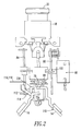
- Figure 2 shows the current path through the circuit breaker 10 of Figure 1.
- the current path is established by a contact assembly 110 including the line terminal 14 and a first fixed contact 72A, the first movable contact 70 to the contact bridge 68 to the second movable contact 70 (not shown), the second movable contact 70 to a second fixed contact 72B, the second fixed contact 72B to a first leg (not shown) of the bimetal 84 by a first flexible conductor 112, through the bimetal 84 to a second leg (not shown) thereof to a second flexible conductor 114, and to the load terminal 16.
- the internal mechanism including, for example, the operating mechanism 134
- the PCBs 120,122 are coupled to the respective case halves 132,130 by employing the screws 146,148 and the nuts 150,152 as shown in Figure 5.
- all electrical connections such as, for example, solder, pin and wire connections, are made prior to over-molding.
- a suitable gap filler (not shown) is employed to prevent the over-molding material from entering the internal operating mechanism 134.
- the assembled device is inserted into suitable mold tooling (not shown) using the screws 146,148 and rivet 154 for proper location and orientation.
- suitable over-molding material is injected into the mold tooling.
- the case halves 130,132 and PCBs 120,122 are inserted into a suitable mold tooling (not shown) as individual entities. Locating holes on the case halves 130,132 and PCBs 120,122 are employed for location within the mold tooling.
- over-molding material is injected into the mold tooling. Vacuum assist or pressurized injection methods may be employed. The over-molding material fills all open voids, thus, encapsulating the PCBs 120,122 and providing a method of joining and sealing the PCBs 120,122 to the respective case halves 132,130. This method also employs via/holes thru the PCBs 120,122 to assist in mechanical coupling.
- the internal operating mechanism 134 is built into the sub-assembly formed by the PCBs 120,122 and case halves 130,132. Then, all solder, pin and wire electrical connections are made. Finally, a secondary cover (not shown) is applied to protect the side opening ( Figure 13).
- Figure 6 shows the assembled circuit breaker 10 with the AFD electronics 120,122 ( Figure 5) being chemically and mechanically linked to the base structure of the respective housing halves 132,130, thereby providing an overall compact and robust electro/mechanical package.
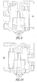
- Figures 7 and 8 show the two AFD printed circuit board assemblies 120 and 122, respectively, of Figure 4.
- the neutral (or, more accurately, the aircraft frame from the bezel 18 of Figure 1) is electrically connected by the two screws 146,148 ( Figure 3) to both of the PCBs 120,122 at pads E5,E6,E7,E8.
- the PCBs 120,122 derive power from voltage between the neutral or frame at pads E5,E6,E7,E8 ( Figures 7 and 8) and the local ground, which is the same potential as the load terminal 16 ( Figure 1).
- the composite structure formed by bonding the AFD printed circuit boards 120,122 (e.g., made of FR4; glass base epoxy binder) and the over-molding material 156 (e.g., made of thermally conductive epoxy coating; a suitable over-molding compound; a suitable potting material) provides improvements in thermal conductivity of the heat of the AFD electronics to the surrounding air through the thermally conductive epoxy coating.
- Over-molding the two AFD printed circuit boards 120,122 to the molded housing halves 130,132 also eliminates the additional space required to package the AFD electronics while providing superior strength, dielectric isolation and thermal heat transfer surface area.
- the housing halves 130,132 provide thermal isolation of the AFD electronics 120,122 from the internal operating mechanism 134 ( Figure 2), such as, for example, in particular, the bimetal 84 and the associated electrical power conductors.
- a suitable trip circuit may implement, for example, the AFD electronics 120,122 in a combination of one or more of analog, digital and/or processor-based circuits, and/or in combination with one or more printed circuit boards (PCBs).
- PCBs printed circuit boards
- an example operating mechanism 134 is disclosed, a wide range of suitable operating mechanisms for electrical switching apparatus may be employed.
Landscapes
- Breakers (AREA)
- Switch Cases, Indication, And Locking (AREA)
Abstract
Description
- This invention relates to electrical switching apparatus and, more particularly, to circuit interrupters, such as, for example, aircraft or aerospace circuit breakers providing arc fault protection.
- Circuit breakers are used to protect electrical circuitry from damage due to an overcurrent condition, such as an overload condition or a relatively high level short circuit or fault condition. In small circuit breakers, commonly referred to as miniature circuit breakers, used for residential and light commercial applications, such protection is typically provided by a thermal-magnetic trip device. This trip device includes a bimetal, which heats and bends in response to a persistent overcurrent condition. The bimetal, in turn, unlatches a spring powered operating mechanism, which opens the separable contacts of the circuit breaker to interrupt current flow in the protected power system.
- Subminiature circuit breakers are used, for example, in aircraft or aerospace electrical systems where they not only provide overcurrent protection but also serve as switches for turning equipment on and off. Such circuit breakers must be small to accommodate the high-density layout of circuit breaker panels, which make circuit breakers for numerous circuits accessible to a user. Aircraft electrical systems, for example, usually consist of hundreds of circuit breakers, each of which is used for a circuit protection function as well as a circuit disconnection function through a push-pull handle.
- Typically, subminiature circuit breakers have provided protection against persistent overcurrents implemented by a latch triggered by a bimetal responsive to I2R heating resulting from the overcurrent. There is a growing interest in providing additional protection, and most importantly arc fault protection.
- During sporadic arc fault conditions, the overload capability of the circuit breaker will not function since the root-mean-squared (RMS) value of the fault current is too small to actuate the automatic trip circuit. The addition of electronic arc fault sensing to a circuit breaker can add one of the elements required for sputtering arc fault protection ― ideally, the output of an electronic arc fault sensing circuit directly trips and, thus, opens the circuit breaker. See, for example, U.S. Patent Nos. 6,710,688; 6,542,056; 6,522,509; 6,522,228; 5,691,869; and 5,224,006.
- The inclusion of arc fault detection electronics into standard, industry sized circuit breakers requires a unique approach to miniaturizing the overall packaging without introducing a significant negative effect on overall device robustness and reliability.
- There is room for improvement in electrical switching apparatus and in housings and trip circuits therefor.
- These needs and others are met by the present invention, in which a housing and a trip circuit cooperate to form a composite structure which comprises at least one printed circuit board and an over-molding material disposed thereon.
- The invention employs molded housing halves that electrically and thermally insulate arc fault detection (AFD) electronics from a current carrying operating mechanism. The AFD electronics are over-molded to the molded housing halves using an over-molding material, such as, for example, a thermally conductive epoxy coating. Over-molding the AFD electronics to the molded housing halves eliminates the additional space required to package such electronics while providing superior strength, dielectric isolation and thermal heat transfer surface area.
- In accordance with one aspect of the invention, an electrical switching apparatus comprises: a housing; separable contacts; an operating mechanism adapted to open and close the separable contacts; and a trip circuit cooperating with the operating mechanism to trip open the separable contacts, wherein the housing and the trip circuit cooperate to form a composite structure which comprises at least one printed circuit board and an over-molding material disposed thereon.
- The housing may include a first housing portion and a second housing portion cooperating with the first housing portion to house the separable contacts and the operating mechanism therein.
- The trip circuit may include a first printed circuit board and a second printed circuit board. The first and second housing portions may form a first surface disposed toward the separable contacts and the operating mechanism, and a second surface and a third surface opposite from the first surface. The first printed circuit board may be coupled to the second surface and the second printed circuit board may be coupled to the third surface.
- The first and second housing portions may be adapted to electrically and thermally insulate the first and second printed circuit boards from the operating mechanism.
- The first and second housing portions may be made of liquid crystal polymer thermoplastic.
- The over-molding material may be a thermally conductive encapsulating material.
- As another aspect of the invention, a circuit breaker comprises: a housing; separable contacts; an operating mechanism adapted to open and close the separable contacts; and a trip circuit cooperating with the operating mechanism to trip open the separable contacts, wherein the housing and the trip circuit cooperate to form an external composite structure which comprises at least one printed circuit board and an over-molding material disposed thereon.
- The trip circuit may include a first printed circuit board and a second printed circuit board. The first and second printed circuit boards may be made of an FR4 electronics substrate having a thickness of about 0.018 inch (about 0.457 mm).
- The trip circuit may include the at least one printed circuit board. The first and second housing portions may form a first surface disposed toward the separable contacts and the operating mechanism and a second surface opposite from the first surface. The at least one printed circuit board may be coupled to the second surface.
- The housing may further include the over-molding material coupling the at least one printed circuit board to the second surface.
- The over-molding material may be a thermally conductive encapsulating material, such as thermally conductive epoxy coating.
- A full understanding of the invention can be gained from the following description of the preferred embodiments when read in conjunction with the accompanying drawings in which:
- Figure 1 is a cross-sectional view of the operating mechanism of a circuit breaker in accordance with the present invention.
- Figure 2 is a vertical elevation view of the opposite side of the operating mechanism of Figure 1.
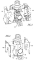
- Figure 3 is an exploded isometric view of a portion of the circuit breaker of Figure 1, which excludes the two arc fault detection (AFD) printed circuit boards of Figure 4.
- Figure 4 is an isometric view of the portion of the circuit breaker of Figure 3 including the operating mechanism housed within two housing halves and further including, in exploded isometric view, the two AFD printed circuit boards.
- Figure 5 is an isometric view of the circuit breaker portion of Figure 4 with the two AFD printed circuit boards in position prior to an over-molding operation which provides the outer base structure of Figure 6.
- Figure 6 is an isometric view of the circuit breaker of Figure 4 including the outer base structure, which is chemically and mechanically coupled to the two AFD printed circuit boards, by the over-molding operation.
- Figures 7 and 8 are plan views of the two AFD printed circuit boards of Figure 4.
- Figures 9 and 10 are top plan views of the two housing halves of Figure 3.
- Figures 11 and 12 are bottom plan views of the two housing halves of Figure 3.
- Figure 13 is a side vertical elevation view of the circuit breaker of Figure 1.
- As employed herein, the statement that two or more parts are "connected" or "coupled" together shall mean that the parts are joined together either directly or joined through one or more intermediate parts.
- As employed herein, the term "composite" means a generally solid material which comprises two or more substances and/or structures (e.g., without limitation, one or more printed circuit boards; an over-molding material) having different physical characteristics and in which each of such substances and/or structures retains its identity while contributing desirable properties to the whole.
- The present invention is described in association with an aircraft or aerospace arc fault circuit breaker, although the invention is applicable to a wide range of electrical switching apparatus, such as, for example, circuit interrupters adapted to detect a wide range of faults, such as, for example, arc faults or ground faults in power circuits.
- Referring to Figure 1, a
circuit breaker 10 comprises anenclosure 12 having a pair ofterminals enclosure 12 for electrical connection to an electrical source and load, respectively. A threaded,conductive ferrule 18 extends exteriorly of theenclosure 12 for the guidance of amanual operator 20 of aplunger assembly 21. Theferrule 18, in conjunction with a nut (not shown), provides a mounting and electrically conductive connection mechanism for thecircuit breaker 10 on a panelboard (not shown). - The
manual operator 20 is provided with atrip indicator 22. Themanual operator 20 andtrip indicator 22 are capable of sliding axial movement with respect to theferrule 18. Themanual operator 20 is provided with acentral portion 24 having acentral slot 26 extending approximately half the length thereof. - A clevis or
thermal latch element 36 is provided with alatch surface 38 and a dependingportion 40. Theclevis 36 is pivotally supported by apin 42 which is movable relative to themanual operator 20 in a slot (not shown). The end portions of thepin 42 are retained within grooves (not shown) in thecentral housing 12 which guide axial movement thereof. - The mechanical latch elements 46 (only one
latch element 46 is shown in Figure 1) are pivotally supported by thepin 42 and are accepted in theslot 26 in themanual operator 20. Thelatch elements 46 are provided with latching surfaces 48 (only onelatching surface 48 is shown in Figure 1) which are adapted to engage a cooperatinglatching surface 50 on theferrule 18. - The
mechanical latch elements 46 have camming apertures 51 (only oneaperture 51 is shown) therein defining camming surfaces 52 (only onecamming surface 52 is shown) which are disposed at an acute angle with respect to the axis of reciprocation of themanual operator 20 thereby to effect manual opening of thecircuit breaker 10. Two lower camming surfaces 54 (only onecamming surface 54 is shown) are disposed at substantially a right angle with respect to the axis of reciprocation of themanual operator 20 to provide positive locking of thecircuit breaker 10. Thecentral stem portion 24 carries acamming pin 56 which extends across theslot 26 therein and through thecamming apertures 51 of themechanical latch elements 46, in order to be in operative engagement therewith. - A
spring 62 is provided to resiliently bias themanual operator 20,clevis 36 and latchelements 46 upwardly with respect to theferrule 18. - A movable contact carrier or
plunger 64 of acontact plunger assembly 65 has acentral opening 66 therein for acceptance of theclevis 36. Thecontact carrier 64 carries a contact bridge 68 (shown in Figure 2) having a pair of movable contacts 70 (only onecontact 70 is shown in Figure 2) positioned thereon. Themovable contacts 70 are engageable with fixed contacts 72 (Figure 2) to complete a circuit from terminal 14 toterminal 16 through a currentresponsive bimetal 84 of thecircuit breaker 10, as will be described. A helical coilplunger return spring 74 abuts against aspring retainer portion 75 of thehousing 12 at one end and themovable contact carrier 64 at its other end, in order to normally bias thecontact carrier 64 upwardly relative to thehousing 12. - The
contact carrier 64 has a laterally extendingslot 78 therein for the acceptance of a thermal oroverload slide 80 and anambient temperature slide 82. Theoverload slide 80 is movable internally of thecontact carrier 64 under the influence of the elongated current responsive bimetal 84, which is retained within thehousing 12 by end supports 85 at each end thereof. - A clevis guide assembly (e.g., made of ceramic) 86 couples the
overload slide 80 to and insulates it from the bimetal 84. Theoverload slide 80 is provided with a slot 88 which accepts and closely cooperates with theclevis 36 to effect pivoting thereof in response to lateral movement of theslide 80. - The
ambient temperature slide 82 underlies theoverload slide 80 and is movable internally of thecontact carrier 64 under the influence of an elongated ambienttemperature compensating bimetal 90, which is part of anambient compensator assembly 92 including anadjustable screw guide 93, a calibratescrew 94 and acompensator spring 95. - The ambient
temperature compensating bimetal 90 is interlocked to theambient temperature slide 82, whereby lateral movement ofsuch slide 82 is controlled, in part, by such bimetal 90. Theambient temperature slide 82 is provided with aslot 96, which, when thecircuit breaker 10 is in the contacts closed position, as shown, accepts thehooked end 40 of theclevis 36. In the contacts closed position, thelatch surface 38 of theclevis 36 engages the upper surface of theambient temperature slide 82 adjacent the periphery of theslot 96 with a pressure determined by the upward resilient bias provided byspring 74. - A
miniature coil assembly 98 includes acoil 100 controlled by AFD PCB2 120 (Figure 7) and aplunger 102. Theplunger 102 is coupled to theambient temperature slide 82, in order to effect an arc fault trip function therewith. - Figure 2 shows the current path through the
circuit breaker 10 of Figure 1. When thecontacts 70,72 are closed, the current path is established by acontact assembly 110 including theline terminal 14 and a firstfixed contact 72A, the firstmovable contact 70 to thecontact bridge 68 to the second movable contact 70 (not shown), the secondmovable contact 70 to a secondfixed contact 72B, the secondfixed contact 72B to a first leg (not shown) of the bimetal 84 by a firstflexible conductor 112, through the bimetal 84 to a second leg (not shown) thereof to a secondflexible conductor 114, and to theload terminal 16. -
Additional conductors PCB2 120 across the bimetal 84, in order to sense current flowing to or from theload terminal 16. - Referring to Figure 3, the enclosure 12 (Figure 1) includes a
lower case half 130 and anupper case half 132. Theinternal operating mechanism 134 is electrically and thermally insulated from the AFD electronics 120,122 (Figure 4). The housing halves 130,132 are preferably made from liquid crystal polymer thermoplastic, which may be molded to provide relatively very thin walls (e.g., without limitation, less than about 0.010 in. (about 0.254 mm)) with an irregular wall thickness and a relatively complex geometry, thereby providing superior strength and temperature insulation characteristics. The housing halves 130,132 also electrically and thermally insulate the AFD electronics 120,122 from the current carryingoperating mechanism 134. - The electrical conductors, such as three pins or terminal couplers 136,138,140, and the two electrical conductors 116,118 (Figures 2 and 13), such as sensing wires, provide a trip signal, a local ground from the
load terminal 16, power (e.g. +5 VDC), a signal from the first bimetal leg towards theseparable contacts 70,72 and away from theload terminal 16, and the second bimetal leg providing the local ground. The three pins 136,138,140 include: (1) the trip signal from thePIC processor 158 onPCB1 122 to PCB2 120, (2) the load terminal 16 (the local ground) fromPCB2 120 toPCB1 122, and (3) +5 VDC fromPCB2 120 toPCB1 122. The electrical connections of the conductors 116,118 are made at feed through holes (not shown) of the respective PCBs 120,122 (Figures 7 and 8). - The
power coil 100 of theminiature coil assembly 98 is disposed through the housing halves 130,132, in order to provide improved heat transfer to the surrounding air. - Two screws 146,148 and two corresponding nuts 150,152 mechanically hold the housing halves 130,132 and the two AFD printed circuit boards 120,122 (Figure 4) and provide the neutral or frame reference thereto from the bezel 18 (Figure 1).
- Figure 4 shows the internal operating mechanism 134 (Figure 3) packaged within the housing halves 130,132, with the AFD electronics 120,122 being shown in an exploded isometric view. Preferably, the AFD printed circuit boards 120 (Figure 7) and 122 (Figure 8) are made of a relatively minimal FR4 electronics substrate (e.g., without limitation, about 0.018 in. (about 0.457 mm) thickness). In contrast, typical printed circuit board thicknesses are about 0.031 in. (about 0.787 mm) to about 0.062 in. (about 1.575 mm). The AFD printed circuit boards 120,122 are then positioned using locating screws 146,148 (Figure 3) prior to over-molding as is discussed, below, in connection with Figure 5. The over-molding of the AFD electronics 120,122 provides the structural and overall package integrity as may be employed, for example, for aerospace use. The housing halves 130,132 are further secured by a
semi-tubular rivet 154. - Figure 5 shows the AFD electronics 120,122 in position prior to the over-molding operation. For example, by employing a thermally conductive encapsulating material 156 (shown exploded for convenience of reference, but after being over-molded) for over-molding, this provides better heat transfer to the surrounding air, increased dielectric protection compared to free air, and superior mechanical integrity of the entire structure. The overall package is minimized using this approach compared to conventional AFCI circuit breakers. This method most importantly shields the AFD electronics 120,122 from common environmental failures, such as, for example, vibration, excessive temperature and dielectric breakdown.
- Examples 1 and 2, below, are examples of different over-molding processes suitable for use with the disclosed
circuit breaker 10. - First, the internal mechanism, including, for example, the
operating mechanism 134, is built into the case halves 130,132 as shown in Figure 3. Next, the PCBs 120,122 are coupled to the respective case halves 132,130 by employing the screws 146,148 and the nuts 150,152 as shown in Figure 5. Then, all electrical connections, such as, for example, solder, pin and wire connections, are made prior to over-molding. A suitable gap filler (not shown) is employed to prevent the over-molding material from entering theinternal operating mechanism 134. Next, the assembled device is inserted into suitable mold tooling (not shown) using the screws 146,148 and rivet 154 for proper location and orientation. Then, suitable over-molding material is injected into the mold tooling. For example, suitable vacuum assist or pressurized injection methods may be employed. The over-molding material fills all open voids, thus, encapsulating the PCBs 120,122, wire connections on the side of the device (Figure 13), and via/holes thru the PCBs 120,122, in order to assist in mechanically coupling to the respective case halves 132,130. Finally, thecircuit breaker 10 is removed from the mold tooling and is de-flashed as needed. - As an alternative to Example 1, the case halves 130,132 and PCBs 120,122 are inserted into a suitable mold tooling (not shown) as individual entities. Locating holes on the case halves 130,132 and PCBs 120,122 are employed for location within the mold tooling. Next, over-molding material is injected into the mold tooling. Vacuum assist or pressurized injection methods may be employed. The over-molding material fills all open voids, thus, encapsulating the PCBs 120,122 and providing a method of joining and sealing the PCBs 120,122 to the respective case halves 132,130. This method also employs via/holes thru the PCBs 120,122 to assist in mechanical coupling. Next, the
internal operating mechanism 134 is built into the sub-assembly formed by the PCBs 120,122 and case halves 130,132. Then, all solder, pin and wire electrical connections are made. Finally, a secondary cover (not shown) is applied to protect the side opening (Figure 13). - Figure 6 shows the assembled
circuit breaker 10 with the AFD electronics 120,122 (Figure 5) being chemically and mechanically linked to the base structure of the respective housing halves 132,130, thereby providing an overall compact and robust electro/mechanical package. - Figures 7 and 8 show the two AFD printed
circuit board assemblies bezel 18 of Figure 1) is electrically connected by the two screws 146,148 (Figure 3) to both of the PCBs 120,122 at pads E5,E6,E7,E8. The PCBs 120,122 derive power from voltage between the neutral or frame at pads E5,E6,E7,E8 (Figures 7 and 8) and the local ground, which is the same potential as the load terminal 16 (Figure 1). - The J100 area of
PCB1 122 with thePIC processor 158 is employed for programming. - Figures 9 and 11 show the
lower housing half 130, and Figures 10 and 12 show theupper housing half 132 of Figure 3. - As shown in Figure 13, the two housing halves 130,132 are both open on one end. For convenience of reference, the three terminal couplers 136,138,140 and the electrical conductors 116,118 are shown exposed, although those components are encapsulated by the
over-molding material 156. - The composite structure formed by bonding the AFD printed circuit boards 120,122 (e.g., made of FR4; glass base epoxy binder) and the over-molding material 156 (e.g., made of thermally conductive epoxy coating; a suitable over-molding compound; a suitable potting material) provides improvements in thermal conductivity of the heat of the AFD electronics to the surrounding air through the thermally conductive epoxy coating. Over-molding the two AFD printed circuit boards 120,122 to the molded housing halves 130,132 also eliminates the additional space required to package the AFD electronics while providing superior strength, dielectric isolation and thermal heat transfer surface area. Furthermore, the housing halves 130,132 provide thermal isolation of the AFD electronics 120,122 from the internal operating mechanism 134 (Figure 2), such as, for example, in particular, the bimetal 84 and the associated electrical power conductors.
- It will be appreciated that a suitable trip circuit may implement, for example, the AFD electronics 120,122 in a combination of one or more of analog, digital and/or processor-based circuits, and/or in combination with one or more printed circuit boards (PCBs). Although an
example operating mechanism 134 is disclosed, a wide range of suitable operating mechanisms for electrical switching apparatus may be employed. - While specific embodiments of the invention have been described in detail, it will be appreciated by those skilled in the art that various modifications and alternatives to those details could be developed in light of the overall teachings of the disclosure. Accordingly, the particular arrangements disclosed are meant to be illustrative only and not limiting as to the scope of the invention which is to be given the full breadth of the claims appended and any and all equivalents thereof.
-
- 10
- circuit breaker
- 12
- enclosure
- 14
- terminal
- 16
- terminal
- 18
- threaded, conductive ferrule
- 20
- manual operator
- 21
- plunger assembly
- 22
- trip indicator
- 24
- central portion
- 26
- central slot
- 36
- clevis or thermal latch element
- 38
- latch surface
- 40
- depending portion
- 42
- pin
- 46
- pair of mechanical latch elements
- 48
- latching surfaces
- 50
- cooperating latching surface
- 51
- camming apertures
- 52
- camming surfaces
- 54
- lower camming surfaces
- 56
- camming pin
- 62
- spring
- 64
- movable contact carrier or plunger
- 65
- contact plunger assembly
- 66
- central opening
- 68
- contact bridge
- 70
- pair of movable contacts
- 72
- fixed contacts (72A,72B)
- 74
- helical coil plunger return spring
- 75
- spring retainer portion
- 78
- laterally extending slot
- 80
- thermal or overload slide
- 82
- ambient temperature slide
- 84
- elongated current responsive bimetal
- 85
- end supports
- 86
- clevis guide assembly (e.g., made of ceramic)
- 88
- slot
- 90
- elongated ambient temperature compensating bimetal
- 92
- ambient compensator assembly
- 93
- adjustable screw guide
- 94
- calibrate screw
- 95
- compensator spring
- 96
- slot
- 98
- miniature coil assembly
- 100
- coil
- 102
- plunger
- 110
- line terminal and contact assembly
- 112
- first flexible conductor
- 114
- second flexible conductor
- 116
- electrical conductor
- 118
- electrical conductor
- 120
- AFD PCB2
- 122
- AFD PCB1
- 130
- lower case half
- 132
- upper case half
- 134
- internal operating mechanism
- 136
- pin or terminal coupler
- 138
- pin or terminal coupler
- 140
- pin or terminal coupler
- 146
- screw
- 148
- screw
- 150
- nut
- 152
- nut
- 154
- semi-tubular rivet
- 156
- thermally conductive encapsulating material
- 158
- PIC processor
Claims (20)
- An electrical switching apparatus (10) comprising:a housing (12);separable contacts (70,72);an operating mechanism (134) adapted to open and close said separable contacts; anda trip circuit (120,122) cooperating with said operating mechanism to trip open said separable contacts,wherein said housing and said trip circuit cooperate to form a composite structure (120,122,130,132,156) which comprises at least one printed circuit board (120,122) and an over-molding material (156) disposed thereon.
- The electrical switching apparatus (10) of Claim 1 wherein said housing comprises a first housing portion (130) and a second housing portion (132) cooperating with said first housing portion to house said separable contacts and said operating mechanism therein.
- The electrical switching apparatus (10) of Claim 2 wherein said trip circuit comprises a first printed circuit board (122) and a second printed circuit board (120); wherein said first and second housing portions form a first surface disposed toward said separable contacts and said operating mechanism, and a second surface and a third surface opposite from said first surface; and wherein said first printed circuit board is coupled to said second surface and said second printed circuit board is coupled to said third surface.
- The electrical switching apparatus (10) of Claim 3 wherein said first and second housing portions are adapted to electrically and thermally insulate said first and second printed circuit boards from said operating mechanism.
- The electrical switching apparatus (10) of Claim 2 wherein said first and second housing portions are made of liquid crystal polymer thermoplastic.
- The electrical switching apparatus (10) of Claim 1 wherein said over-molding material is a thermally conductive encapsulating material (156).
- A circuit breaker (10) comprising:a housing (12);separable contacts (70,72);an operating mechanism (134) adapted to open and close said separable contacts; anda trip circuit (120,122) cooperating with said operating mechanism to trip open said separable contacts,wherein said housing and said trip circuit cooperate to form an external composite structure (120,122,130,132,156) which comprises at least one printed circuit board (120,122) and an over-molding material (156) disposed thereon.
- The circuit breaker (10) of Claim 7 wherein said housing comprises a first housing portion (130) and a second housing portion (132) cooperating with said first housing portion to house said separable contacts and said operating mechanism therein.
- The circuit breaker (10) of Claim 8 wherein at least a portion of said first and second housing portions includes a structure disposed intermediate: (a) said separable contacts and said operating mechanism, and (b) said at least one printed circuit board.
- The circuit breaker (10) of Claim 8 wherein said trip circuit comprises a first printed circuit board (120) and a second printed circuit board (122); wherein said first and second housing portions form a first surface disposed toward said separable contacts and said operating mechanism, and a second surface and a third surface opposite from said first surface; and wherein said first printed circuit board is coupled to said second surface and said second printed circuit board is coupled to said third surface.
- The circuit breaker (10) of Claim 10 wherein said first and second printed circuit boards are made of an FR4 electronics substrate having a thickness of about 0.018 inch (about 0.457 mm).
- The circuit breaker (10) of Claim 10 wherein said housing further comprises two fasteners (146,148,150,152) coupling said first housing portion, said second housing portion and said first and second printed circuit boards.
- The circuit breaker (10) of Claim 10 wherein said operating mechanism comprises a plurality of electrical conductors (136,138,140) electrically connected between said first and second printed circuit boards.
- The circuit breaker (10) of Claim 8 wherein said trip circuit comprises said at least one printed circuit board (120,122); wherein said first and second housing portions form a first surface disposed toward said separable contacts and said operating mechanism and a second surface opposite from said first surface; and wherein said at least one printed circuit board is coupled to said second surface.
- The circuit breaker (10) of Claim 14 wherein said first and second housing portions are adapted to electrically and thermally insulate said first and second printed circuit boards from said operating mechanism.
- The circuit breaker (10) of Claim 15 wherein said first and second housing portions are made of liquid crystal polymer thermoplastic.
- The circuit breaker (10) of Claim 15 wherein said first and second housing portions include a structure disposed intermediate: (a) said separable contacts and said operating mechanism, and (b) each of said first and second printed circuit boards.
- The circuit breaker (10) of Claim 14 wherein said housing further comprises said over-molding material coupling said at least one printed circuit board to said second surface.
- The circuit breaker (10) of Claim 18 wherein said over-molding material is a thermally conductive encapsulating material (156).
- The circuit breaker (10) of Claim 19 wherein said thermally conductive encapsulating material is a thermally conductive epoxy coating (156).
Applications Claiming Priority (1)
| Application Number | Priority Date | Filing Date | Title |
|---|---|---|---|
| US11/008,463 US7170376B2 (en) | 2004-12-09 | 2004-12-09 | Electrical switching apparatus including a housing and a trip circuit forming a composite structure |
Publications (3)
| Publication Number | Publication Date |
|---|---|
| EP1670013A2 true EP1670013A2 (en) | 2006-06-14 |
| EP1670013A3 EP1670013A3 (en) | 2007-08-22 |
| EP1670013B1 EP1670013B1 (en) | 2009-09-23 |
Family
ID=35954892
Family Applications (1)
| Application Number | Title | Priority Date | Filing Date |
|---|---|---|---|
| EP05026827A Expired - Lifetime EP1670013B1 (en) | 2004-12-09 | 2005-12-08 | Electrical switching apparatus including a housing and a trip circuit forming a composite structure |
Country Status (3)
| Country | Link |
|---|---|
| US (1) | US7170376B2 (en) |
| EP (1) | EP1670013B1 (en) |
| DE (1) | DE602005016766D1 (en) |
Cited By (3)
| Publication number | Priority date | Publication date | Assignee | Title |
|---|---|---|---|---|
| WO2009153644A1 (en) * | 2008-06-16 | 2009-12-23 | Eaton Corporation | Method of electrically grounding an electrical switching apparatus and electrical switching apparatus including the same |
| WO2012080828A3 (en) * | 2010-12-17 | 2012-11-15 | Eaton Corporation | Electrical system, and circuit protection module and electrical switching apparatus therefor |
| CN103996575A (en) * | 2014-05-09 | 2014-08-20 | 安庆天瑞新材料科技股份有限公司 | Thermomagnetic breaker capable of current detection and communication |
Families Citing this family (16)
| Publication number | Priority date | Publication date | Assignee | Title |
|---|---|---|---|---|
| US7518475B2 (en) * | 2007-07-24 | 2009-04-14 | Eaton Corporation | Electrical switching apparatus, circuit interrupter and method of interrupting overcurrents of a power circuit |
| US7570146B2 (en) * | 2007-07-25 | 2009-08-04 | Eaton Corporation | Circuit breaker including ambient compensation bimetal holding and releasing arc fault indicator |
| US7576471B1 (en) * | 2007-09-28 | 2009-08-18 | Triquint Semiconductor, Inc. | SAW filter operable in a piston mode |
| US8971055B2 (en) * | 2008-12-16 | 2015-03-03 | Schneider Electric USA, Inc. | Residential circuit breaker with flexible printed circuit boards |
| US7994882B2 (en) * | 2009-04-18 | 2011-08-09 | General Electric Company | Space allocation within a circuit breaker |
| US8138864B2 (en) | 2009-06-01 | 2012-03-20 | Eaton Corporation | Circuit interrupter including a molded case made of liquid crystal polymer |
| US8514552B2 (en) | 2010-12-17 | 2013-08-20 | Eaton Corporation | Electrical system and matrix assembly therefor |
| CA2837110C (en) * | 2011-06-21 | 2018-11-20 | Eaton Corporation | Sealed plug-in circuit breaker assembly |
| US9270090B2 (en) * | 2011-06-27 | 2016-02-23 | Labinal, Llc | Grounded circuit breaker panel electrical module and method for grounding same |
| DE102013008128A1 (en) * | 2012-05-15 | 2013-11-21 | Marquardt Mechatronik Gmbh | Electric switch |
| EP3050068B1 (en) * | 2013-09-26 | 2023-06-21 | Labinal, LLC | Circuit breaker module with plug-in circuit breakers |
| EP3078051B1 (en) | 2013-12-03 | 2019-02-06 | Labinal, LLC | Electrical switching apparatus including a remotely controllable actuator structured to move a push/pull operating handle |
| KR101869724B1 (en) * | 2017-01-05 | 2018-06-21 | 엘에스산전 주식회사 | Magnetic trip device for circuit breaker |
| KR102299858B1 (en) * | 2017-03-15 | 2021-09-08 | 엘에스일렉트릭 (주) | Magnetic trip mechanism for circuit breaker |
| WO2018217883A2 (en) | 2017-05-23 | 2018-11-29 | Pass & Seymour, Inc. | Arc fault circuit interrupter |
| US10468219B2 (en) * | 2017-09-07 | 2019-11-05 | Carling Technologies, Inc. | Circuit interrupter with status indication |
Family Cites Families (22)
| Publication number | Priority date | Publication date | Assignee | Title |
|---|---|---|---|---|
| US4092623A (en) | 1976-07-21 | 1978-05-30 | Mechanical Products | Circuit breaker |
| US4110719A (en) | 1977-04-11 | 1978-08-29 | Mechanical Products | Three phase circuit breaker |
| US4415875A (en) | 1982-05-18 | 1983-11-15 | Mechanical Products, Inc. | Circuit breaker |
| US4568899A (en) * | 1984-03-27 | 1986-02-04 | Siemens Aktiengesellschaft | Ground fault accessory for a molded case circuit breaker |
| US4667263A (en) * | 1985-04-22 | 1987-05-19 | General Electric Company | Ground fault module for ground fault circuit breaker |
| US4652975A (en) * | 1986-04-28 | 1987-03-24 | General Electric Company | Mounting arrangement for circuit breaker current sensing transformers |
| US4725799A (en) * | 1986-09-30 | 1988-02-16 | Westinghouse Electric Corp. | Circuit breaker with remote control |
| JP2925402B2 (en) * | 1991-09-11 | 1999-07-28 | 三菱電機株式会社 | Circuit breaker having a housing formed by molding a high thermal conductivity, low shrinkage wet-type unsaturated polyester resin composition |
| US5224006A (en) | 1991-09-26 | 1993-06-29 | Westinghouse Electric Corp. | Electronic circuit breaker with protection against sputtering arc faults and ground faults |
| US5691869A (en) | 1995-06-06 | 1997-11-25 | Eaton Corporation | Low cost apparatus for detecting arcing faults and circuit breaker incorporating same |
| US6522509B1 (en) | 2000-07-21 | 2003-02-18 | Eaton Corporation | Arc fault detection in ac electric power systems |
| US6633222B2 (en) * | 2000-08-08 | 2003-10-14 | Furukawa Precision Engineering Co., Ltd. | Battery breaker |
| US6307749B1 (en) * | 2000-10-23 | 2001-10-23 | Delphi Technologies, Inc. | Overmolded electronic module with underfilled surface-mount components |
| US6710688B2 (en) | 2001-04-30 | 2004-03-23 | Eaton Corporation | Circuit breaker |
| US6522228B2 (en) * | 2001-04-30 | 2003-02-18 | Eaton Corporation | Circuit breaker including an arc fault trip actuator having an indicator latch and a trip latch |
| US6542056B2 (en) | 2001-04-30 | 2003-04-01 | Eaton Corporation | Circuit breaker having a movable and illuminable arc fault indicator |
| US6842325B2 (en) * | 2001-09-19 | 2005-01-11 | Square D Company | Flexible circuit adhered to metal frame of device |
| US6538862B1 (en) * | 2001-11-26 | 2003-03-25 | General Electric Company | Circuit breaker with a single test button mechanism |
| US6545574B1 (en) * | 2001-12-17 | 2003-04-08 | General Electric Company | Arc fault circuit breaker |
| US6700138B2 (en) * | 2002-02-25 | 2004-03-02 | Silicon Bandwidth, Inc. | Modular semiconductor die package and method of manufacturing thereof |
| ES2294279T3 (en) * | 2002-03-08 | 2008-04-01 | Kearney-National, Inc. | MOLDED RELAY OF SURFACE MOUNT AND THE MANUFACTURING METHOD OF THE SAME. |
| US7038337B2 (en) * | 2003-05-20 | 2006-05-02 | Siemens Vdo Automotive Corporation | EMI suppression in permanent magnet DC motors having PCB outside motor in connector and overmolded |
-
2004
- 2004-12-09 US US11/008,463 patent/US7170376B2/en not_active Expired - Lifetime
-
2005
- 2005-12-08 DE DE602005016766T patent/DE602005016766D1/en not_active Expired - Lifetime
- 2005-12-08 EP EP05026827A patent/EP1670013B1/en not_active Expired - Lifetime
Cited By (6)
| Publication number | Priority date | Publication date | Assignee | Title |
|---|---|---|---|---|
| WO2009153644A1 (en) * | 2008-06-16 | 2009-12-23 | Eaton Corporation | Method of electrically grounding an electrical switching apparatus and electrical switching apparatus including the same |
| WO2012080828A3 (en) * | 2010-12-17 | 2012-11-15 | Eaton Corporation | Electrical system, and circuit protection module and electrical switching apparatus therefor |
| US8445800B2 (en) | 2010-12-17 | 2013-05-21 | Eaton Corporation | Electrical system, and circuit protection module and electrical switching apparatus therefor |
| CN103262196A (en) * | 2010-12-17 | 2013-08-21 | 伊顿公司 | Electrical system and its circuit protection module and electrical switching device |
| CN103262196B (en) * | 2010-12-17 | 2015-11-25 | 雷比诺有限责任公司 | Electrical system and its circuit protection module and electrical switching device |
| CN103996575A (en) * | 2014-05-09 | 2014-08-20 | 安庆天瑞新材料科技股份有限公司 | Thermomagnetic breaker capable of current detection and communication |
Also Published As
| Publication number | Publication date |
|---|---|
| US7170376B2 (en) | 2007-01-30 |
| EP1670013B1 (en) | 2009-09-23 |
| EP1670013A3 (en) | 2007-08-22 |
| US20060125583A1 (en) | 2006-06-15 |
| DE602005016766D1 (en) | 2009-11-05 |
Similar Documents
| Publication | Publication Date | Title |
|---|---|---|
| EP1670013B1 (en) | Electrical switching apparatus including a housing and a trip circuit forming a composite structure | |
| EP3078090B1 (en) | Method and apparatus for sensing the status of a circuit interrupter | |
| EP0706712B1 (en) | Ground fault module conductors and base therefor | |
| CN101211728B (en) | Earth leakage circuit breaker | |
| US9362075B2 (en) | Cover assembly for circuit breaker, circuit breaker having the same, and method | |
| JPH02230629A (en) | Auxiliary switching element of circuit breaker | |
| US9852851B2 (en) | Molded case circuit breaker with current sensing unit | |
| US5252937A (en) | Molded case circuit breaker modular bell alarm unit | |
| EP2259282B1 (en) | Circuit interrupter including a molded case made of liquid crystal polymer | |
| CN100446149C (en) | Leakage circuit breakers | |
| CN101483121B (en) | Electronic trip device case for a circuit breaker, electronic trip device and assembly method thereof | |
| US7948724B2 (en) | Current transformer support bracket and circuit interrupter including the same | |
| KR100763648B1 (en) | Male / switchboard with overheat monitoring | |
| US9754753B2 (en) | Breaker secondary terminal block isolation chamber | |
| JP3318583B2 (en) | Earth leakage breaker | |
| JP4012098B2 (en) | Earth leakage breaker | |
| WO2007125410A2 (en) | Arc fault circuit interrupter with plug-on neutral contact clip spring | |
| US20090310324A1 (en) | Method of electrically grounding an electrical switching apparatus and electrical switching apparatus including the same | |
| US4415875A (en) | Circuit breaker | |
| JPH0785768A (en) | Earth leakage circuit breaker | |
| JPH06267395A (en) | Earth leakage breaker | |
| JP2000173438A (en) | Earth leakage breaker | |
| CN116913736A (en) | Status Indicating Device with Wide Operating Range for Low Current Applications |
Legal Events
| Date | Code | Title | Description |
|---|---|---|---|
| PUAI | Public reference made under article 153(3) epc to a published international application that has entered the european phase |
Free format text: ORIGINAL CODE: 0009012 |
|
| AK | Designated contracting states |
Kind code of ref document: A2 Designated state(s): AT BE BG CH CY CZ DE DK EE ES FI FR GB GR HU IE IS IT LI LT LU LV MC NL PL PT RO SE SI SK TR |
|
| AX | Request for extension of the european patent |
Extension state: AL BA HR MK YU |
|
| PUAL | Search report despatched |
Free format text: ORIGINAL CODE: 0009013 |
|
| AK | Designated contracting states |
Kind code of ref document: A3 Designated state(s): AT BE BG CH CY CZ DE DK EE ES FI FR GB GR HU IE IS IT LI LT LU LV MC NL PL PT RO SE SI SK TR |
|
| AX | Request for extension of the european patent |
Extension state: AL BA HR MK YU |
|
| AKX | Designation fees paid | ||
| 17P | Request for examination filed |
Effective date: 20071102 |
|
| RBV | Designated contracting states (corrected) |
Designated state(s): DE FR GB |
|
| GRAJ | Information related to disapproval of communication of intention to grant by the applicant or resumption of examination proceedings by the epo deleted |
Free format text: ORIGINAL CODE: EPIDOSDIGR1 |
|
| GRAP | Despatch of communication of intention to grant a patent |
Free format text: ORIGINAL CODE: EPIDOSNIGR1 |
|
| GRAS | Grant fee paid |
Free format text: ORIGINAL CODE: EPIDOSNIGR3 |
|
| GRAA | (expected) grant |
Free format text: ORIGINAL CODE: 0009210 |
|
| AK | Designated contracting states |
Kind code of ref document: B1 Designated state(s): DE FR GB |
|
| REG | Reference to a national code |
Ref country code: GB Ref legal event code: FG4D |
|
| REF | Corresponds to: |
Ref document number: 602005016766 Country of ref document: DE Date of ref document: 20091105 Kind code of ref document: P |
|
| PLBE | No opposition filed within time limit |
Free format text: ORIGINAL CODE: 0009261 |
|
| STAA | Information on the status of an ep patent application or granted ep patent |
Free format text: STATUS: NO OPPOSITION FILED WITHIN TIME LIMIT |
|
| 26N | No opposition filed |
Effective date: 20100624 |
|
| REG | Reference to a national code |
Ref country code: FR Ref legal event code: PLFP Year of fee payment: 11 |
|
| REG | Reference to a national code |
Ref country code: FR Ref legal event code: PLFP Year of fee payment: 12 |
|
| REG | Reference to a national code |
Ref country code: FR Ref legal event code: PLFP Year of fee payment: 13 |
|
| REG | Reference to a national code |
Ref country code: GB Ref legal event code: 732E Free format text: REGISTERED BETWEEN 20181115 AND 20181130 |
|
| REG | Reference to a national code |
Ref country code: DE Ref legal event code: R082 Ref document number: 602005016766 Country of ref document: DE Ref country code: DE Ref legal event code: R081 Ref document number: 602005016766 Country of ref document: DE Owner name: EATON INTELLIGENT POWER LIMITED, IE Free format text: FORMER OWNER: EATON CORP., CLEVELAND, OHIO, US |
|
| P01 | Opt-out of the competence of the unified patent court (upc) registered |
Effective date: 20230521 |
|
| PGFP | Annual fee paid to national office [announced via postgrant information from national office to epo] |
Ref country code: DE Payment date: 20241121 Year of fee payment: 20 |
|
| PGFP | Annual fee paid to national office [announced via postgrant information from national office to epo] |
Ref country code: GB Payment date: 20241122 Year of fee payment: 20 |
|
| PGFP | Annual fee paid to national office [announced via postgrant information from national office to epo] |
Ref country code: FR Payment date: 20241121 Year of fee payment: 20 |
|
| REG | Reference to a national code |
Ref country code: DE Ref legal event code: R071 Ref document number: 602005016766 Country of ref document: DE |
|
| REG | Reference to a national code |
Ref country code: GB Ref legal event code: PE20 Expiry date: 20251207 |