EP1667495A2 - Organic semiconductor device and method for manufacturing same - Google Patents
Organic semiconductor device and method for manufacturing same Download PDFInfo
- Publication number
- EP1667495A2 EP1667495A2 EP04772542A EP04772542A EP1667495A2 EP 1667495 A2 EP1667495 A2 EP 1667495A2 EP 04772542 A EP04772542 A EP 04772542A EP 04772542 A EP04772542 A EP 04772542A EP 1667495 A2 EP1667495 A2 EP 1667495A2
- Authority
- EP
- European Patent Office
- Prior art keywords
- organic semiconductor
- electrode
- injecting electrode
- semiconductor device
- electron injecting
- Prior art date
- Legal status (The legal status is an assumption and is not a legal conclusion. Google has not performed a legal analysis and makes no representation as to the accuracy of the status listed.)
- Withdrawn
Links
Images




Classifications
-
- H—ELECTRICITY
- H10—SEMICONDUCTOR DEVICES; ELECTRIC SOLID-STATE DEVICES NOT OTHERWISE PROVIDED FOR
- H10K—ORGANIC ELECTRIC SOLID-STATE DEVICES
- H10K10/00—Organic devices specially adapted for rectifying, amplifying, oscillating or switching; Organic capacitors or resistors having potential barriers
- H10K10/80—Constructional details
- H10K10/82—Electrodes
- H10K10/84—Ohmic electrodes, e.g. source or drain electrodes
-
- H—ELECTRICITY
- H10—SEMICONDUCTOR DEVICES; ELECTRIC SOLID-STATE DEVICES NOT OTHERWISE PROVIDED FOR
- H10K—ORGANIC ELECTRIC SOLID-STATE DEVICES
- H10K50/00—Organic light-emitting devices
- H10K50/10—OLEDs or polymer light-emitting diodes [PLED]
- H10K50/17—Carrier injection layers
- H10K50/171—Electron injection layers
-
- H—ELECTRICITY
- H10—SEMICONDUCTOR DEVICES; ELECTRIC SOLID-STATE DEVICES NOT OTHERWISE PROVIDED FOR
- H10K—ORGANIC ELECTRIC SOLID-STATE DEVICES
- H10K50/00—Organic light-emitting devices
- H10K50/80—Constructional details
- H10K50/805—Electrodes
- H10K50/82—Cathodes
-
- H—ELECTRICITY
- H10—SEMICONDUCTOR DEVICES; ELECTRIC SOLID-STATE DEVICES NOT OTHERWISE PROVIDED FOR
- H10K—ORGANIC ELECTRIC SOLID-STATE DEVICES
- H10K50/00—Organic light-emitting devices
- H10K50/80—Constructional details
- H10K50/805—Electrodes
- H10K50/82—Cathodes
- H10K50/822—Cathodes characterised by their shape
-
- H—ELECTRICITY
- H10—SEMICONDUCTOR DEVICES; ELECTRIC SOLID-STATE DEVICES NOT OTHERWISE PROVIDED FOR
- H10K—ORGANIC ELECTRIC SOLID-STATE DEVICES
- H10K59/00—Integrated devices, or assemblies of multiple devices, comprising at least one organic light-emitting element covered by group H10K50/00
- H10K59/80—Constructional details
- H10K59/805—Electrodes
- H10K59/8052—Cathodes
- H10K59/80521—Cathodes characterised by their shape
-
- H—ELECTRICITY
- H10—SEMICONDUCTOR DEVICES; ELECTRIC SOLID-STATE DEVICES NOT OTHERWISE PROVIDED FOR
- H10K—ORGANIC ELECTRIC SOLID-STATE DEVICES
- H10K71/00—Manufacture or treatment specially adapted for the organic devices covered by this subclass
- H10K71/60—Forming conductive regions or layers, e.g. electrodes
-
- H—ELECTRICITY
- H10—SEMICONDUCTOR DEVICES; ELECTRIC SOLID-STATE DEVICES NOT OTHERWISE PROVIDED FOR
- H10K—ORGANIC ELECTRIC SOLID-STATE DEVICES
- H10K77/00—Constructional details of devices covered by this subclass and not covered by groups H10K10/80, H10K30/80, H10K50/80 or H10K59/80
- H10K77/10—Substrates, e.g. flexible substrates
-
- H—ELECTRICITY
- H10—SEMICONDUCTOR DEVICES; ELECTRIC SOLID-STATE DEVICES NOT OTHERWISE PROVIDED FOR
- H10K—ORGANIC ELECTRIC SOLID-STATE DEVICES
- H10K85/00—Organic materials used in the body or electrodes of devices covered by this subclass
- H10K85/60—Organic compounds having low molecular weight
- H10K85/615—Polycyclic condensed aromatic hydrocarbons, e.g. anthracene
- H10K85/621—Aromatic anhydride or imide compounds, e.g. perylene tetra-carboxylic dianhydride or perylene tetracarboxylic di-imide
-
- Y—GENERAL TAGGING OF NEW TECHNOLOGICAL DEVELOPMENTS; GENERAL TAGGING OF CROSS-SECTIONAL TECHNOLOGIES SPANNING OVER SEVERAL SECTIONS OF THE IPC; TECHNICAL SUBJECTS COVERED BY FORMER USPC CROSS-REFERENCE ART COLLECTIONS [XRACs] AND DIGESTS
- Y02—TECHNOLOGIES OR APPLICATIONS FOR MITIGATION OR ADAPTATION AGAINST CLIMATE CHANGE
- Y02E—REDUCTION OF GREENHOUSE GAS [GHG] EMISSIONS, RELATED TO ENERGY GENERATION, TRANSMISSION OR DISTRIBUTION
- Y02E10/00—Energy generation through renewable energy sources
- Y02E10/50—Photovoltaic [PV] energy
- Y02E10/549—Organic PV cells
-
- Y—GENERAL TAGGING OF NEW TECHNOLOGICAL DEVELOPMENTS; GENERAL TAGGING OF CROSS-SECTIONAL TECHNOLOGIES SPANNING OVER SEVERAL SECTIONS OF THE IPC; TECHNICAL SUBJECTS COVERED BY FORMER USPC CROSS-REFERENCE ART COLLECTIONS [XRACs] AND DIGESTS
- Y02—TECHNOLOGIES OR APPLICATIONS FOR MITIGATION OR ADAPTATION AGAINST CLIMATE CHANGE
- Y02P—CLIMATE CHANGE MITIGATION TECHNOLOGIES IN THE PRODUCTION OR PROCESSING OF GOODS
- Y02P70/00—Climate change mitigation technologies in the production process for final industrial or consumer products
- Y02P70/50—Manufacturing or production processes characterised by the final manufactured product
-
- Y—GENERAL TAGGING OF NEW TECHNOLOGICAL DEVELOPMENTS; GENERAL TAGGING OF CROSS-SECTIONAL TECHNOLOGIES SPANNING OVER SEVERAL SECTIONS OF THE IPC; TECHNICAL SUBJECTS COVERED BY FORMER USPC CROSS-REFERENCE ART COLLECTIONS [XRACs] AND DIGESTS
- Y10—TECHNICAL SUBJECTS COVERED BY FORMER USPC
- Y10S—TECHNICAL SUBJECTS COVERED BY FORMER USPC CROSS-REFERENCE ART COLLECTIONS [XRACs] AND DIGESTS
- Y10S428/00—Stock material or miscellaneous articles
- Y10S428/917—Electroluminescent
Definitions
- the present invention relates to an organic semiconductor device of an arrangement wherein electrons are injected from an electron injecting electrode into organic semiconductor layers, and a method for manufacturing the organic semiconductor device.
- An organic electroluminescence element which is a typical example of an organic semiconductor device, is a light emitting element that makes use of a light emitting phenomenon that accompanies the recombination of electrons and holes in organic semiconductor layers.
- an organic electroluminescence element includes organic semiconductor light emitting layers, an electron injecting electrode that injects electrons into the organic semiconductor light emitting layers, and a hole injecting electrode that injects holes into the organic semiconductor light emitting layers (see Japanese Unexamined Patent Publication No. 5-315078 (1993)).
- the electron injecting electrode must be made from a material of high electron injection efficiency
- the hole injecting electrode must be made from a material of high hole injection efficiency, and a material of low work function is thus required for the electron injecting electrode.
- an Mg film is a likely candidate for the material of the electron injecting electrode, an Mg film oxidizes readily and is chemicallyunstable. Since anMg film does not have a sufficient adhesive force to a base film and either is impossible to form into a film or peels off readily even if formed into a film, it is low in reliability and not fit for practical use.
- MgAg alloys and MgIn alloys have thus been used as materials of the electron injecting electrode, with these materials, the electron injection efficiency is inadequate and separation of the electron injecting electrode occurs when continuous light emitting operation is performed over a long period of time (see Japanese Unexamined Patent Publication No. 5-315078).
- an MgAg alloy is inadequate in durability against lithography processes using such organic solvents as acetone and IPA (isopropyl alcohol) and is unsuited for preparing an electron injecting electrode with a microscopic structure such as a comb-like shape.
- Japanese Unexamined Patent Publication No. 5-315078 discloses the forming of an electron injecting electrode with a two-layer structure of an Mg layer and an Au layer on light emitting layers, a base layer to which the Mg layer can be adhered is limited, and such a structure cannot be realized depending on the type of the base layer.
- a base layer to which the Mg layer can be adhered is limited, and such a structure cannot be realized depending on the type of the base layer.
- the electron injecting electrode of the above arrangement cannot be employed in a case where an electron injecting electrode with a microscopic structure is to be prepared.
- An object of the present invention is to provide an organic semiconductor device, having an electron injecting electrode that is high in electron injection efficiency and is high in reliability, and a method for manufacturing such an organic semiconductor device.
- Another obj ect of the present invention is to provide an organic semiconductor device, having an electron injecting electrode that can be microfabricated by a lithography process, and a method for manufacturing such an organic semiconductor device.
- An organic semiconductor device comprises: an organic semiconductor layer; and an electron injecting electrode, formed of an MgAu alloy and injecting electrons into the above-mentioned organic semiconductor layer.
- Au gold
- Au is used widely as an electrode material of semiconductor devices, it has been considered to be inappropriate as a material of an electron injecting electrode of an organic semiconductor device due to its high work function. Also, there is a stereotype concept that Au generally does not form alloys, and there has thus not been an example of forming an electron injecting electrode from an Au alloy.
- an alloy of Au and Mg (magnesium) can be formed, and the MgAu alloy has been confirmed to be close in work function to the work function of Mg, be high in electron injection efficiency in comparison to MgAg alloys and other generally used electron injecting electrode materials, and exhibit good adhesion properties regardless of the type of a base layer. More specifically, good adhesion properties are exhibited even with respect to silicon oxide films and peeling does not occur even after the elapse of a long period of time.
- MgAu alloy has also been confirmed to exhibit a unique chemical stability, is far more chemically stable than MgAg alloys, and is also good in corrosion resistance against organic solvents.
- MgAu alloy withstands lithography processes using organic solvents such as acetone and IPA (isopropyl alcohol), it can be used to prepare a microscopic electrode structure, such as that of comb-teeth-like shape.
- An electron injecting electrode formed of MgAu alloy also exhibits adequate durability even with continuous driving.
- an organic semiconductor device having an electron injecting electrode that is high in electron injection efficiency and is high in reliability, can be realized, and an organic semiconductor device, having an electron injecting electrode that can be microprocessed by a lithography process, can be realized.
- MgAu alloy forming the above-mentioned electron injecting electrode preferably contains not more than 85 atom % of Au.
- the Au content of the MgAu alloy forming the electron injecting electrode is greater than 0 and not more than 85 atom %.
- Such an MgAu alloy exhibits a low work function close to the work function of Mg and exhibits chemically stable properties.
- the Au content of the MgAu alloy is preferably not less than 0.1 atom % and more preferably not less than 1 atom %.
- the chemical stability of the electron injecting electrode can thereby be improved and the sheet resistance of the electron injecting electrode can be reduced.
- the above-mentioned organic semiconductor device also includes a hole injecting electrode that injects holes into the organic semiconductor layer.
- the hole injecting electrode may be formed of MgAu alloy or may be formed of a material other than MgAu alloy.
- the electron injecting electrode and the hole injecting electrode respectively have comb-teeth-like portions kept apart from each other in a manner whereby the electrodes virtually fit to each other.
- the electrodes can be shaped to comb-teeth-like shapes.
- the electron injecting electrode and the hole injecting electrode have mutually-fitting comb-teeth-like portions that are kept apart by an interval (a microscopic interval)
- the total length of the portions of the electron injecting electrode and the hole injecting electrode that oppose each other can be made long.
- the recombination of holes and electrons can thus be made to occur effectively.
- Low-voltage drive is thereby enabled, and in the case where the organic semiconductor layer is an organic semiconductor light-emitting layer, a high light emitting efficiency can be realized.
- the comb-teeth portions with microscopic widths so that the light emission will be recognized visually as a surface emitting state, a practically surface emitting light source can be realized.
- the organic semiconductor device furthermore includes a gate electrode that opposes, via an insulating film, a region of the organic semiconductor layer between the electron injecting electrode and the hole injecting electrode.
- an FET (field effect transistor) type organic semiconductor device can be realized, and the recombination of electrons and holes in the organic semiconductor layer can be controlled by a control voltage provided to the gate electrode.
- on/off control of light emission can be performed by providing binary control voltages of a high level and a low level to the gate electrode, or gradation control of the light emission intensity can be performed by providing, to the gate electrode, a stepless control voltage that is controlled in a continuous manner or multiple value control voltages that are controlled in a stepwise manner.
- the electron injecting electrode and the hole injecting electrode are formed so as to contact the insulating film and be spaced apart at an interval in a direction parallel to the insulating film, and the organic semiconductor layer is formed on the insulating film in a region between the electron injecting electrode and the hole injecting electrode.
- MgAu alloy film can be formed regardless of a type of the base film and can be formed with a good adhesion property even on a silicon oxide film, which is a typical insulating film.
- the device is of a bottom contact type structure, wherein the electron injecting electrode and the hole injecting electrode are disposed on the insulating film and the organic semiconductor layer is disposed so as to cover these components, the device with high reliability can be realized.
- the organic semiconductor layer With the bottom contact structure, with which the organic semiconductor layer can be formed after forming the electron injecting electrode and the hole injecting electrode, the organic semiconductor layer will not be exposed to the organic solvents used in microprocessing the electron injecting electrode and the hole injecting electrode. The merit that the electron injecting electrode and the hole injecting electrode of microscopic structures can be formed without damaging the organic semiconductor layer is thus provided.
- the organic semiconductor device may take on a top contact structure, wherein the electron injecting electrode and the hole injecting electrode are formed on the organic semiconductor layer (for example, formed by lamination on an insulating film).
- the organic semiconductor layer for example, formed by lamination on an insulating film.
- Mg and Au are preferably vaporized using a boat of low radiant heat (a microscopic boat) to form a vapor deposited film of MgAu alloy on the surface of the organic semiconductor layer.
- the organic semiconductor layer may include an organic semiconductor light emitting layer that emits light by recombination of electrons injected by the electron injecting electrode and holes injected from the hole injecting electrode. With this arrangement, the recombination of holes and electrons in an organic semiconductor light emitting layer allows light to emit.
- the organic semiconductor device may furthermore include an electron takeout electrode for taking out electrons from the organic semiconductor layer.
- an electron takeout electrode for taking out electrons from the organic semiconductor layer.
- the electron injecting electrode and the electrode takeout electrode respectively have comb-teeth-like portions positioned apart from each other in a manner whereby the electrodes virtually fit mutually as if put inmutual contact.
- the electrodes can be shaped to comb-teeth-like shapes. Since by making the electron injecting electrode and the electron takeout electrode have mutually-fitting comb-teeth-like portions that are kept apart by an interval (a microscopic interval), the total length of the portions of the electron injecting electrode and the electron takeout electrode that oppose each other can be made long, electrons move efficiently inside the organic semiconductor light-emitting layer. A low voltage drive is thus enabled.
- the organic semiconductor device furthermore includes a gate electrode that opposes, via an insulating film, a region of the organic semiconductor layer between the electron injecting electrode and the electron takeout electrode.
- an FET (field effect transistor) type organic semiconductor device can be realized, and the movement of electrons in the organic semiconductor layer can be controlled by a control voltage provided to the gate electrode.
- the organic semiconductor device can thereby be made to perform on/off operations as a switching element or perform an amplifying operation.
- the electron injecting electrode and the electron takeout electrode are formed so as to contact the insulating film and be spaced apart at an interval in a direction parallel to the insulating film, and the organic semiconductor layer is formed on the insulating film in a region between the electron injecting electrode and the electron takeout electrode.
- An organic semiconductor device manufacturing method comprises the steps of: forming an electrode film, formed of MgAu alloy, on a substrate; forming electrodes by patterning the electrode film through a lithography process; and forming an organic semiconductor layer so as to cover the electrodes that are formed.
- the lithography process can be performed on the electrode film formed of MgAu alloy, electrodes (at least an electron injecting electrode, and preferably both an electron injecting electrode and a hole injecting electrode) of microscopic structures can be formed.
- electrodes at least an electron injecting electrode, and preferably both an electron injecting electrode and a hole injecting electrode
- the organic semiconductor layer will not be exposed to organic solvents used in the lithography process and the organic semiconductor layer can be made to possess predetermined characteristics.
- the electrodes are formed of MgAu alloy, the electrodes have good durability against the lithography process and do not become peeled from the substrate.
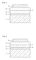
- FIG. 1 is a schematic sectional view for describing an arrangement of an organic semiconductor device according to a first embodiment of the present invention.
- This organic semiconductor device is a so-called organic electroluminescence element, and is arranged by forming a hole injecting electrode 2, formed of an ITO (a solid solution of indium oxide (In 2 O 3 ) and tin oxide (SnO 2 )) film, on a glass substrate 1; laminating a hole transport layer 3, formed of an ⁇ -NPD (Bis[N-(1-naphthyl)-N-phenyl]benzidine) layer, on a hole injecting electrode 2; laminating an electron transport layer 4, formed of an Alq3 (Tris-(8-hydroxyquinoline)aluminum) layer, on the hole transport layer 3; and laminating an electron injecting electrode 5, formed of an MgAu alloy film, on the electron transport layer 4.
- a hole injecting electrode 2 formed of an ITO (a solid solution of indium oxide (In 2 O 3
- the hole transport layer 3 and the electron transport layer 4 make up an organic semiconductor layer, and in the present embodiment, the electron transport layer 4, formed of the Alq3 layer, makes up an organic semiconductor light emitting layer.
- the hole injecting electrode 2 has a film thickness of 110nm
- hole transport layer 3 has a film thickness of 50nm
- electron transport layer 4 has a film thickness of 50nm
- electron injecting electrode 5 has a film thickness of 100nm.
- FIG. 2 is a schematic sectional view for describing an arrangement of an organic semiconductor device according to a modification of the arrangement shown in FIG. 1.
- respective components corresponding to components of FIG. 1 are provided with the same reference numerals as those of FIG. 1.
- a hole injection layer 8 formed of CuPc (copperphthalocyanine), is interposed between the hole injecting electrode 2 and the hole transport layer 3.
- the hole injection layer 8 is made 10nm in film thickness
- the hole transport layer 3 is made 40nm in film thickness
- the other respective layers are made to be the same in film thickness as in the arrangement of FIG. 1.
- FIG. 3 is a schematic view for describing a method for forming the electron injecting electrode 5.
- the glass substrate 1, on which the hole injecting electrode 2, the hole transport layer 3, and the electron transport layer 4 (and the hole injection layer 8 in the case of the arrangement of FIG. 2) have been formed, is held facing downward inside a vacuum chamber 10.
- These boats 11 and 12 are, for example, resistance heating types and enable control of the vaporization rate.
- Both those boats 11 and 12 are microscopic and are arranged so that effects on the organic semiconductor layers (hole transport layer 3 and electron transport layer 4, and furthermore hole injection layer 8 in the case of the arrangement of FIG.
- the substrate temperature is set, for example, to room temperature. It is considered that effects of oxygen, etc., can be better lessened to restrain degradation when the degree of vacuum inside vacuum chamber 10 increases, and in general, the degree of vacuum inside vacuum chamber 10 is preferably set to not more than 1 x 10 -3 Pa.
- electron injecting electrode 5, formed of the MgAu alloy film can be formed on the electron transport layer 4.
- the atomic ratio of MgAu alloy that makes up the electron injecting electrode 5 can be controlled.
- FIG. 4 (a) is a diagram of operation characteristics of the organic semiconductor device with the structure of FIG. 1 and shows relationships between the drive voltage applied across the hole injecting electrode 2 and the electron injecting electrode 5 and the results of measuring the current density at each drive voltage.
- a curve L1 shows the operation characteristics of the device with the structure of FIG. 1, and a curve L2 shows the operation characteristics for the case where MgAg alloy is used for the electron injecting electrode 5.
- a comparison of the curves L1 and L2 shows that by forming the electron injecting electrode from MgAu alloy, even at the same drive voltage the current density is made higher than in the case where the electron injecting electrode is formed of MgAg alloy. It can thus be understood that by forming the electron injecting electrode from MgAu alloy, the electron injection efficiency is improved and consequently, low voltage drive is realized.
- FIG. 4 (b) is a diagram showing the relationships of quantum efficiency (light emitting efficiency) with respect to the current density in the organic semiconductor device with the structure of FIG. 1.
- a curve L11 shows the results of measuring the quantum efficiency of the device of the structure of FIG. 1
- a curve L12 shows the results of measuring the quantum efficiency for the case where MgAg alloy is used for electron injecting electrode 5.
- a comparison of the curves L11 and L12 shows that the quantum efficiency is lower when the electron injecting electrode is formed of MgAu alloy than when MgAg alloy makes up the electron injecting alloy, this is presumed to be caused by a breakdown of balance between the hole injection efficiency and the electron injection efficiency due to the use of MgAu alloy of good electron injection efficiency.
- the diffusion of Au atoms into the organic semiconductor layer due to radiant heat from the Au vapor deposition source can be cited as another cause.
- FIG. 5 (a) is a diagram of operation characteristics of the organic semiconductor device with the structure of FIG. 2 and shows relationships between the drive voltage applied across the hole injecting electrode 2 and the electron injecting electrode 5 and the results of measuring the current density at each drive voltage.
- a curve L21 shows the operation characteristics of the device of the structure of FIG. 2, and a curve L22 shows the operation characteristics for the case where MgAg alloy is used for the electron injecting electrode 5.
- a comparison of the curves L21 and L22 shows that by forming the electron injecting electrode from MgAu alloy, the same operation characteristics as those in the case where the electron injecting electrode is formed of MgAg alloy can be realized.
- FIG. 5 (b) is a diagram showing the relationships of quantum efficiency (light emitting efficiency) with respect to the current density in the organic semiconductor device with the structure of FIG. 2.
- a curve L31 shows the results of measuring the quantum efficiency of the device of the structure of FIG. 2
- a curve L32 shows the results of measuring the quantum efficiency for the case where MgAg alloy is used for electron injecting electrode 5.
- a comparison of the curves L31 and L32 shows that the quantum efficiency is higher when the electron injecting electrode is formed of MgAu alloy than when MgAg alloy makes up the electron injecting alloy. This is presumed to be due to the harmonization of the efficiency of injection of electrons from the electron injecting electrode formed of MgAu alloy and the hole injection efficiency due to the introduction of the hole injection layer 8.
- FIGS. 4 (a) and 4 (b) and FIGS. 5 (a) and 5 (b) show that the arrangement of the organic semiconductor layer can be selected according to the desired device characteristics (low-voltage drive, high light emitting efficiency, etc.) and that the excellent characteristics of the organic semiconductor device, in which the electron injecting electrode is formed from MgAu alloy, can thereby be brought out.
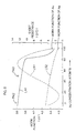
- FIG. 6 is a diagram of results of measuring relationships between Au atom content and work function and between Au atom content and sheet resistance of an MgAu alloy thin film with a thickness of 40nm.
- a curve L41 indicates measured values of the work function and a curve L51 indicates measured values of the sheet resistance.
- Points P42 and P43 indicate measured values of the work function of an MgAg alloy thin film, and a curve L52 indicates measured values of the sheet resistance of the MgAg alloy thin film.
- the curve L41 shows that when the Au atom content is not more than 85 atom %, the work function becomes 4.0eV or less and becomes closer in value to the work function of Mg alone than the work function of Au alone and thus good electron injection efficiency can be anticipated.
- the curve L51 shows that when the Au atom content is in the range of 5 to 25 atom %, the sheet resistance becomes substantially equal in value to that of Au alone and a low-resistance electrode film can be realized.
- FIG. 7 is a schematic sectional view for describing an arrangement of an organic semiconductor device according to a second embodiment of the present invention.
- This organic semiconductor device is an element having the basic structure of an FET (field effect transistor) (unipolar type organic semiconductor FET) and is arranged by forming a silicon oxide film 22 as an insulating film on a gate electrode 21 that is formed of an n + silicon substrate into which an impurity has been introduced at a high concentration, forming a source electrode 23 as an electron injecting electrode and a drain electrode 24 as an electron takeout electrode in a manner such that the electrodes are spaced apart by an interval on the silicon oxide film 22, and forming an organic semiconductor layer 25 so as to cover and be interposed between the source electrode 23 and the drain electrode 24.
- This structure is called a bottom contact structure since the source electrode 23 and the drain electrode 24 are positioned at the substrate (gate electrode 21) side with respect to the organic semiconductor layer 25.
- the source electrode 23 and the drain electrode 24 are both formed of an MgAu alloy thin film (with a film thickness, for example, of 40nm) and are formed along the surface of the silicon oxide film 22 (that is, along the gate electrode 21 as the substrate) so as to oppose each other while being separated by a microscopic interval (for example, of 25 ⁇ m).
- the organic semiconductor layer 25 is present in a region between the source electrode 23 and the drain electrode 24, and the gate electrode 21 opposes the organic semiconductor layer 25 of this region with the silicon oxide film 22 interposed in between.
- the organic semiconductor device can be made to operate as a switching element that performs an on/off operation. Also by applying, to the gate electrode 21, a control voltage that varies in a stepless manner or multiple value control voltages that vary in multiple steps of three steps or more, the current that flows between the source and drain can be varied in multiple steps and a current control operation (amplifying operation) can thereby be performed.
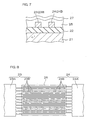
- the source electrode 23 and the drain electrode 24 respectively have main body portions 23A and 24A and a plurality (ten each in the example of FIG. 8) of comb-teeth portions 23B and 24B that protrude in parallel to each other from the main body portions 23A and 24B.
- the electrodes are positioned on the silicon oxide film 22 so that the comb-teeth portions 23B and 24B fit mutually with a microscopic interval in between. Since the each comb-teeth portion 23B of the source electrode 23 opposes the comb-teeth portion 24B of the drain electrode 24 at both of its sides, the total length of the portions of the source electrode 23 and the drain electrode 24 that practically oppose each other is made long.
- the respective efficiencies of the injection of electrons into the organic semiconductor layer 25 and the takeout of electrons from the organic semiconductor layer 25 are thereby made high and driving at a low voltage is enabled.
- FIGS. 9(a) to 9(f) are schematic sectional views showing, in the order of steps, a method for manufacturing the organic semiconductor device of FIG. 7.
- the silicon oxide film 22 is formed on the gate electrode 21 (silicon substrate) (FIG. 9 (a)) .
- a resist film 31 is then formed, for example, by spin coating, on the surface of the gate electrode 21 serving as the substrate on which the silicon oxide film 22 was formed (see FIG. 9(b)).
- a mask 40 having openings 40a at regions corresponding to the source electrode 23 and the drain electrode 24, is then positioned above the resist film 31 (see FIG. 9 (c)) .
- Ultraviolet rays (UV) are then irradiate via the mask 40 and the resist film 31 is thereby exposed.
- the resist film 31 is then developed by a developing solution.
- the exposed regions of the resist film 31 are modified and dissolve in the developing solution.
- the unexposed regions do not dissolve in the developing solution due to the properties being maintained.
- the exposed regions of the resist film 31 are thus dissolved and the openings 31a are formed (see FIG. 9(d)).
- Mg atoms and Au atoms are supplied to the resist film 31 and exposed portions of the silicon oxide film 22 in openings 31a, andMgAu alloy thin films 32 are thereby formed over the entire surface (see FIG. 9(e)).
- the MgAu alloy thin film 32 outside openings 31a is lifted off, and the MgAu alloy thin films 32 at portions corresponding to the openings 31a remain as the source electrode 23 and the drain electrode 24 on the silicon oxide film 22 (see FIG. 9 (f)).
- the organic semiconductor layer 25 so as to cover the entireties of the exposed surfaces of the source electrode 23, the drain electrode 24, and the silicon oxide film 22, the organic semiconductor device of the arrangement shown in FIG. 7 is obtained.
- the substrate is immersed in an acetone solution and subjected to ultrasonic vibration in the immersed state. Thereafter, the substrate is immersed in IPA and subjected to ultrasonic vibration, and then an IPA boiling process is performed.
- the MgAu alloy film does not undergo undesirable corrosion, and the source electrode 23 and the drain electrode 24 that are adhered well on the substrate (gate electrode 21) can be obtained.
- the present inventors observed the source electrode 23 and the drain electrode 24 adhered to the silicon oxide film 22 in a satisfactory pattern. A change of this state was not observed even when applying a treatment using the organic solvents (acetone and IPA) after a period of one week.
- FIG. 10 is a diagramof results of measuring operation characteristics (FET characteristics) of the organic semiconductor device of FIG. 7.
- results of the same measurements performed on an arrangement with the source electrode 23 and the drain electrode 24 being formed from the MgAg alloy thin films are indicated by an alternate long and two short dashes line.
- C 6 -PTC (see chemical formula [F1] below) was used as the organic semiconductor layer 25, and the measurements were made in vacuum (3.2 x 10 -1 Pa).
- FIG. 11 shows results of measuring the electron mobility in the organic semiconductor device of FIG. 7 and a variation of the electron mobility with respect to the Au atom concentration of the MgAu thin film that makes up the source electrode23andthedrainelectrode24.
- the film thickness of the MgAu thin film was 40nm and C 6 -PTC was used as the organic semiconductor layer 25.
- C 8 -PTC, C 12 -PTC, C 13 -PTC, Bu-PTC, F 7 Bu-PTC*, Ph-PTC, F 5 Ph-PTC*, PTCDI, TCNQ, C 60 fullerene, etc. may be used besides C 6 -PTC as the organic semiconductormaterial making up the organic semiconductor layer 25. All of these are organic semiconductor materials that exhibit characteristics as N-type semiconductors and can give rise to movement of electrons in their interiors.
- a third embodiment according to the present invention shall now be described with reference to FIGS. 7, 8, etc., with description being omitted for components that are the same as those of the above-described second embodiment.
- the drain electrode 24 functions as an electron takeout electrode
- the drain electrode 24 functions as a hole injecting electrode
- organic semiconductor material making up the organic semiconductor layer 25 ⁇ -NPD, Alq3, BSA-1m (9,10-Bis(3-cyanostilil)anthracene), MEHPPV (Poly[2-methoxy-5-(2-ethylhexyloxy)-1,4-phenyleneviny lene]), CN-PPP(Poly[2-(6-cynao-6-methylheptyloxy)-1,4-phenylene]), Bis(2-(2-hydroxyphenyl)-benz-1,3-thiazolato)zinc complex, Poly[(9,9-dihexylfluoren-2,7-diyl)-co-(anthracen-9,10-diyl) ] and other bipolar organic semiconductor materials can be used, and the organic semiconductor layer 25 can thus be made to function as an organic semiconductor light emitting layer.
- the organic semiconductor device can be controlled between a lit state and an unlit state.
- a control voltage that varies in a stepless manner or multiple value control voltages that vary in multiple steps of three steps or more the light emission intensity can be varied in a stepless or multiple step manner and a multiple gradation display can thus be performed.
- each of the comb-teeth portions 23B and 24B are formed to a microscopic width (for example, 50nm) and the gate electrode 21 opposes the entirety of a rectangular region 28 in which comb-teeth portions 23B and 24B overlap, this rectangular region 28 is visually recognized as a surface emitting light source during light emission.
- each comb-teeth portion 23B of the source electrode 23 opposes a comb-teeth portion 24B of the drain electrode 24 at both of its sides, the total length of the portions of the source electrode 23 and the drain electrode 24 that practically oppose each other is made long.
- the respective injection efficiencies of electrons and holes into the organic semiconductor layer 25 are thus made high and light emitting operation at a high efficiency is enabled.
- a method for manufacturing the device according to this embodiment is the same as that in the case of the second embodiment described above.
- a buffer layer for reducing an energy barrier may be interposed between the electron injecting electrode and the organic semiconductor layer or between the hole injecting electrode (or electron takeout electrode) and the organic semiconductor layer.
- a buffer layer formed of PEDOT poly(ethylenedioxy)thiophene
- the buffer layer formed of PEDOT acts to reduce the energy barrier between the light emitting layer formed of MEHPPV and the hole injecting electrode (or electron takeout electrode) formed, for example, of ITO, and to reduce the energy barrier between the light emitting layer formed of MEHPPV and the electron injecting electrode formed of MgAu alloy.
- the light emitted in the organic semiconductor layer 25 can be taken out upon being converted in wavelength at the wavelength conversion layer 27 and light of a desired color can thus be emitted.
- a gate electrode may be formed apart from the substrate. That is, a thin film gate electrode may be formed on a substrate of any of various types, such as a silicon substrate, a substrate having a silicon oxide layer formed on a silicon substrate, a silicon nitride substrate, a glass substrate, or a sapphire substrate. Such a gate electrode canbe formed fromapolysilicon film, nickel thin film, aluminum thin film, etc., that have been lowered in resistance by the addition of impurity at a high concentration.
- the gate electrode may be formed not on the substrate side but on the organic semiconductor layer as shown in FIG. 12.
- FIG. 12 portions corresponding to the respective portions shown in FIG. 7 are provided with the same reference numerals as those of FIG. 7.
- the insulating film interposed between the gate electrode and the organic semiconductor layer maybe formedof tantalumpentoxide, aluminum oxide, a polymer (such as novolac resin, polyimide, etc.).
Landscapes
- Physics & Mathematics (AREA)
- Optics & Photonics (AREA)
- Engineering & Computer Science (AREA)
- Spectroscopy & Molecular Physics (AREA)
- Chemical & Material Sciences (AREA)
- Materials Engineering (AREA)
- Manufacturing & Machinery (AREA)
- Electroluminescent Light Sources (AREA)
- Thin Film Transistor (AREA)
- Electrodes Of Semiconductors (AREA)
Abstract
Description
- The present invention relates to an organic semiconductor device of an arrangement wherein electrons are injected from an electron injecting electrode into organic semiconductor layers, and a method for manufacturing the organic semiconductor device.
- An organic electroluminescence element, which is a typical example of an organic semiconductor device, is a light emitting element that makes use of a light emitting phenomenon that accompanies the recombination of electrons and holes in organic semiconductor layers. Specifically, an organic electroluminescence element includes organic semiconductor light emitting layers, an electron injecting electrode that injects electrons into the organic semiconductor light emitting layers, and a hole injecting electrode that injects holes into the organic semiconductor light emitting layers (see Japanese Unexamined Patent Publication No. 5-315078 (1993)).
- To improve the light emitting efficiency, the electron injecting electrode must be made from a material of high electron injection efficiency, the hole injecting electrode must be made from a material of high hole injection efficiency, and a material of low work function is thus required for the electron injecting electrode.
- Though from the standpoint of the work function, an Mg film is a likely candidate for the material of the electron injecting electrode, an Mg film oxidizes readily and is chemicallyunstable. Since anMg film does not have a sufficient adhesive force to a base film and either is impossible to form into a film or peels off readily even if formed into a film, it is low in reliability and not fit for practical use.
- Though MgAg alloys and MgIn alloys have thus been used as materials of the electron injecting electrode, with these materials, the electron injection efficiency is inadequate and separation of the electron injecting electrode occurs when continuous light emitting operation is performed over a long period of time (see Japanese Unexamined Patent Publication No. 5-315078). Moreover, an MgAg alloy is inadequate in durability against lithography processes using such organic solvents as acetone and IPA (isopropyl alcohol) and is unsuited for preparing an electron injecting electrode with a microscopic structure such as a comb-like shape.
- Though Japanese Unexamined Patent Publication No. 5-315078 discloses the forming of an electron injecting electrode with a two-layer structure of an Mg layer and an Au layer on light emitting layers, a base layer to which the Mg layer can be adhered is limited, and such a structure cannot be realized depending on the type of the base layer. For example, when an electron injecting electrode is to be formed on a silicon oxide film, since an Mg layer will not adhere to the silicon oxide film, the above structure cannot be employed. Moreover, since the Mg layer is not durable against lithography processes using organic solvents, the electron injecting electrode of the above arrangement cannot be employed in a case where an electron injecting electrode with a microscopic structure is to be prepared.
- An object of the present invention is to provide an organic semiconductor device, having an electron injecting electrode that is high in electron injection efficiency and is high in reliability, and a method for manufacturing such an organic semiconductor device.
- Another obj ect of the present invention is to provide an organic semiconductor device, having an electron injecting electrode that can be microfabricated by a lithography process, and a method for manufacturing such an organic semiconductor device.
- An organic semiconductor device according to the present invention comprises: an organic semiconductor layer; and an electron injecting electrode, formed of an MgAu alloy and injecting electrons into the above-mentioned organic semiconductor layer.
- Though Au (gold) is used widely as an electrode material of semiconductor devices, it has been considered to be inappropriate as a material of an electron injecting electrode of an organic semiconductor device due to its high work function. Also, there is a stereotype concept that Au generally does not form alloys, and there has thus not been an example of forming an electron injecting electrode from an Au alloy.
- According to research by the present inventors, an alloy of Au and Mg (magnesium) can be formed, and the MgAu alloy has been confirmed to be close in work function to the work function of Mg, be high in electron injection efficiency in comparison to MgAg alloys and other generally used electron injecting electrode materials, and exhibit good adhesion properties regardless of the type of a base layer. More specifically, good adhesion properties are exhibited even with respect to silicon oxide films and peeling does not occur even after the elapse of a long period of time.
- MgAu alloy has also been confirmed to exhibit a unique chemical stability, is far more chemically stable than MgAg alloys, and is also good in corrosion resistance against organic solvents. For example, since MgAu alloy withstands lithography processes using organic solvents such as acetone and IPA (isopropyl alcohol), it can be used to prepare a microscopic electrode structure, such as that of comb-teeth-like shape. An electron injecting electrode formed of MgAu alloy also exhibits adequate durability even with continuous driving.
- Thus by the present invention, an organic semiconductor device, having an electron injecting electrode that is high in electron injection efficiency and is high in reliability, can be realized, and an organic semiconductor device, having an electron injecting electrode that can be microprocessed by a lithography process, can be realized.
- MgAu alloy forming the above-mentioned electron injecting electrode preferably contains not more than 85 atom % of Au.
- That is, preferably the Au content of the MgAu alloy forming the electron injecting electrode is greater than 0 and not more than 85 atom %. Such an MgAu alloy exhibits a low work function close to the work function of Mg and exhibits chemically stable properties.
- The Au content of the MgAu alloy is preferably not less than 0.1 atom % and more preferably not less than 1 atom %. The chemical stability of the electron injecting electrode can thereby be improved and the sheet resistance of the electron injecting electrode can be reduced.
- Preferably, the above-mentioned organic semiconductor device also includes a hole injecting electrode that injects holes into the organic semiconductor layer. The hole injecting electrode may be formed of MgAu alloy or may be formed of a material other than MgAu alloy.
- Preferably, the electron injecting electrode and the hole injecting electrode respectively have comb-teeth-like portions kept apart from each other in a manner whereby the electrodes virtually fit to each other.
- As mentioned above, since microprocessing by a lithography process can be performed on MgAu alloy, the electrodes can be shaped to comb-teeth-like shapes. By making the electron injecting electrode and the hole injecting electrode have mutually-fitting comb-teeth-like portions that are kept apart by an interval (a microscopic interval), the total length of the portions of the electron injecting electrode and the hole injecting electrode that oppose each other can be made long. The recombination of holes and electrons can thus be made to occur effectively. Low-voltage drive is thereby enabled, and in the case where the organic semiconductor layer is an organic semiconductor light-emitting layer, a high light emitting efficiency can be realized. By forming the comb-teeth portions with microscopic widths so that the light emission will be recognized visually as a surface emitting state, a practically surface emitting light source can be realized.
- Preferably, the organic semiconductor device furthermore includes a gate electrode that opposes, via an insulating film, a region of the organic semiconductor layer between the electron injecting electrode and the hole injecting electrode.
- With this arrangement, an FET (field effect transistor) type organic semiconductor device can be realized, and the recombination of electrons and holes in the organic semiconductor layer can be controlled by a control voltage provided to the gate electrode. Thus when the organic semiconductor layer is made from an organic semiconductor light emitting layer, on/off control of light emission can be performed by providing binary control voltages of a high level and a low level to the gate electrode, or gradation control of the light emission intensity can be performed by providing, to the gate electrode, a stepless control voltage that is controlled in a continuous manner or multiple value control voltages that are controlled in a stepwise manner.
- Preferably, the electron injecting electrode and the hole injecting electrode are formed so as to contact the insulating film and be spaced apart at an interval in a direction parallel to the insulating film, and the organic semiconductor layer is formed on the insulating film in a region between the electron injecting electrode and the hole injecting electrode.
- With this arrangement, since the electron injecting electrode and the hole injecting electrode are formed on the insulating film, microprocessing of the electron injecting electrode and the hole injecting electrode by a lithography process can be performed prior to forming the organic semiconductor layer. As mentioned above, MgAu alloy film can be formed regardless of a type of the base film and can be formed with a good adhesion property even on a silicon oxide film, which is a typical insulating film. Thus even if the device is of a bottom contact type structure, wherein the electron injecting electrode and the hole injecting electrode are disposed on the insulating film and the organic semiconductor layer is disposed so as to cover these components, the device with high reliability can be realized.
- Moreover, with the bottom contact structure, with which the organic semiconductor layer can be formed after forming the electron injecting electrode and the hole injecting electrode, the organic semiconductor layer will not be exposed to the organic solvents used in microprocessing the electron injecting electrode and the hole injecting electrode. The merit that the electron injecting electrode and the hole injecting electrode of microscopic structures can be formed without damaging the organic semiconductor layer is thus provided.
- Needless to say, the organic semiconductor device according to the present invention may take on a top contact structure, wherein the electron injecting electrode and the hole injecting electrode are formed on the organic semiconductor layer (for example, formed by lamination on an insulating film). However in this case, it is preferable not to apply a lithography process for patterning the electron injecting electrode and the hole injecting electrode but to apply a process of forming electrodes of desiredpatterns on the organic semiconductor layer by selective vapor deposition of the materials of the electron injecting electrode and the hole injecting electrode onto the organic semiconductor layer via a predetermined mask.
- Also, to minimize thermal effects on the organic semiconductor layer, Mg and Au are preferably vaporized using a boat of low radiant heat (a microscopic boat) to form a vapor deposited film of MgAu alloy on the surface of the organic semiconductor layer.
- The organic semiconductor layer may include an organic semiconductor light emitting layer that emits light by recombination of electrons injected by the electron injecting electrode and holes injected from the hole injecting electrode. With this arrangement, the recombination of holes and electrons in an organic semiconductor light emitting layer allows light to emit.
- The organic semiconductor device may furthermore include an electron takeout electrode for taking out electrons from the organic semiconductor layer. By this arrangement, a semiconductor device of a form, wherein electrons move from the electron injecting electrode to the electron takeout electrode through the organic semiconductor layer, can be realized.
- Preferably, the electron injecting electrode and the electrode takeout electrode respectively have comb-teeth-like portions positioned apart from each other in a manner whereby the electrodes virtually fit mutually as if put inmutual contact.
- As mentioned above, since microprocessing by a lithography process can be performed on MgAu alloy, the electrodes can be shaped to comb-teeth-like shapes. Since by making the electron injecting electrode and the electron takeout electrode have mutually-fitting comb-teeth-like portions that are kept apart by an interval (a microscopic interval), the total length of the portions of the electron injecting electrode and the electron takeout electrode that oppose each other can be made long, electrons move efficiently inside the organic semiconductor light-emitting layer. A low voltage drive is thus enabled.
- Preferably, the organic semiconductor device furthermore includes a gate electrode that opposes, via an insulating film, a region of the organic semiconductor layer between the electron injecting electrode and the electron takeout electrode.
- With this arrangement, an FET (field effect transistor) type organic semiconductor device can be realized, and the movement of electrons in the organic semiconductor layer can be controlled by a control voltage provided to the gate electrode. The organic semiconductor device can thereby be made to perform on/off operations as a switching element or perform an amplifying operation.
- Preferably, the electron injecting electrode and the electron takeout electrode are formed so as to contact the insulating film and be spaced apart at an interval in a direction parallel to the insulating film, and the organic semiconductor layer is formed on the insulating film in a region between the electron injecting electrode and the electron takeout electrode.
- With this arrangement, since the electron injecting electrode and the electron takeout electrode are formed on the insulating film, microprocessing of the electron injecting electrode and the electron takeout electrode by a lithography process can be performed prior to forming the organic semiconductor layer.
- An organic semiconductor device manufacturing method according to the present invention comprises the steps of: forming an electrode film, formed of MgAu alloy, on a substrate; forming electrodes by patterning the electrode film through a lithography process; and forming an organic semiconductor layer so as to cover the electrodes that are formed.
- By the present invention, since the lithography process can be performed on the electrode film formed of MgAu alloy, electrodes (at least an electron injecting electrode, and preferably both an electron injecting electrode and a hole injecting electrode) of microscopic structures can be formed. By thereafter forming the organic semiconductor layer, the organic semiconductor layer will not be exposed to organic solvents used in the lithography process and the organic semiconductor layer can be made to possess predetermined characteristics.
- Moreover, since the electrodes are formed of MgAu alloy, the electrodes have good durability against the lithography process and do not become peeled from the substrate.
- The above and other objects, characteristics, and advantages of the present invention will be made clear by the following description of the embodiments made in reference to the attached drawings.
-
- FIG. 1 is a schematic sectional view for describing an arrangement of an organic semiconductor device according to a first embodiment of the present invention.
- FIG. 2 is a schematic sectional view for describing an arrangement of an organic semiconductor device according to a modification of the arrangement shown in FIG. 1.
- FIG. 3 is a schematic view for describing a method for forming an electron injecting electrode.
- FIGS. 4(a) and 4(b) are diagrams of characteristics of the organic semiconductor device with the structure of FIG. 1.
- FIGS. 5(a) and 5(b) are diagrams of operation characteristics of the organic semiconductor device with the structure of FIG. 2.
- FIG. 6 is a diagram of results of measuring relationships between Au atom content and work function and between Au atom content and sheet resistance with respect to an MgAu alloy thin film.
- FIG. 7 is a schematic sectional view for describing an arrangement of an organic semiconductor device according to a second embodiment and a third embodiment of the present invention.
- FIG. 8 is a plan view of shapes of a source electrode and drain electrode.
- FIGS. 9(a) to 9(f) are schematic sectional views showing, in the order of steps, a method for manufacturing the organic semiconductor device of FIG. 7.
- FIG. 10 is a diagram of results of measuring operation characteristics (FET characteristics) of the organic semiconductor device of FIG. 7.
- FIG. 11 is a diagram of results of measuring the electron mobility in the organic semiconductor device of FIG. 7.
- FIG. 12 is a schematic sectional view of another configuration of a gate electrode.
- FIG. 1 is a schematic sectional view for describing an arrangement of an organic semiconductor device according to a first embodiment of the present invention. This organic semiconductor device is a so-called organic electroluminescence element, and is arranged by forming a
hole injecting electrode 2, formed of an ITO (a solid solution of indium oxide (In2O3) and tin oxide (SnO2)) film, on aglass substrate 1; laminating ahole transport layer 3, formed of an α-NPD (Bis[N-(1-naphthyl)-N-phenyl]benzidine) layer, on ahole injecting electrode 2; laminating anelectron transport layer 4, formed of an Alq3 (Tris-(8-hydroxyquinoline)aluminum) layer, on thehole transport layer 3; and laminating anelectron injecting electrode 5, formed of an MgAu alloy film, on theelectron transport layer 4. - The
hole transport layer 3 and theelectron transport layer 4 make up an organic semiconductor layer, and in the present embodiment, theelectron transport layer 4, formed of the Alq3 layer, makes up an organic semiconductor light emitting layer. For example, thehole injecting electrode 2 has a film thickness of 110nm,hole transport layer 3 has a film thickness of 50nm,electron transport layer 4 has a film thickness of 50nm, andelectron injecting electrode 5 has a film thickness of 100nm. - When a predetermined drive voltage, with which the
hole injecting electrode 2 side is positive, is applied across thehole injecting electrode 2 and theelectron injecting electrode 5, holes are injected into thehole transport layer 3 from thehole injecting electrode 2 and electrons are injected into theelectron transport layer 4 from theelectron injecting electrode 5. These holes and electrons are transported to the interface betweenhole transport layer 3 andelectron transport layer 4 and recombine and emit light in alight emitting region 7 inside theelectron transport layer 4 near the interface. - FIG. 2 is a schematic sectional view for describing an arrangement of an organic semiconductor device according to a modification of the arrangement shown in FIG. 1. In FIG. 2, respective components corresponding to components of FIG. 1 are provided with the same reference numerals as those of FIG. 1.
- With the arrangement of FIG. 2, a
hole injection layer 8, formed of CuPc (copperphthalocyanine), is interposed between thehole injecting electrode 2 and thehole transport layer 3. By the function of thehole injection layer 8, the injection efficiency of holes is increased and the light emitting efficiency is improved. For example, thehole injection layer 8 is made 10nm in film thickness, thehole transport layer 3 is made 40nm in film thickness, and the other respective layers are made to be the same in film thickness as in the arrangement of FIG. 1. - FIG. 3 is a schematic view for describing a method for forming the
electron injecting electrode 5. Theglass substrate 1, on which thehole injecting electrode 2, thehole transport layer 3, and the electron transport layer 4 (and thehole injection layer 8 in the case of the arrangement of FIG. 2) have been formed, is held facing downward inside avacuum chamber 10. Inside thevacuum chamber 10 are positioned a boat (crucible) 11 for vaporizing Mg and aboat 12 for vaporizing Au. Theseboats boats hole transport layer 3 andelectron transport layer 4, and furthermore holeinjection layer 8 in the case of the arrangement of FIG. 8) due to radiant heat from the boats are minimized. The substrate temperature is set, for example, to room temperature. It is considered that effects of oxygen, etc., can be better lessened to restrain degradation when the degree of vacuum insidevacuum chamber 10 increases, and in general, the degree of vacuum insidevacuum chamber 10 is preferably set to not more than 1 x 10⁻³Pa. - With such an arrangement, by vaporizing Mg and Au from the
boats electron transport layer 4 on theglass substrate 1,electron injecting electrode 5, formed of the MgAu alloy film, can be formed on theelectron transport layer 4. By positioning amask 13, having an opening with dimensions and a shape corresponding to theelectron injecting electrode 5, near thesubstrate 1 and at the side of theboats electron injecting electrode 5 of the desire shape can be formed on theelectron transport layer 4. Also by adjusting the rates of vaporization from theboats electron injecting electrode 5 can be controlled. - FIG. 4 (a) is a diagram of operation characteristics of the organic semiconductor device with the structure of FIG. 1 and shows relationships between the drive voltage applied across the
hole injecting electrode 2 and theelectron injecting electrode 5 and the results of measuring the current density at each drive voltage. A curve L1 shows the operation characteristics of the device with the structure of FIG. 1, and a curve L2 shows the operation characteristics for the case where MgAg alloy is used for theelectron injecting electrode 5. - A comparison of the curves L1 and L2 shows that by forming the electron injecting electrode from MgAu alloy, even at the same drive voltage the current density is made higher than in the case where the electron injecting electrode is formed of MgAg alloy. It can thus be understood that by forming the electron injecting electrode from MgAu alloy, the electron injection efficiency is improved and consequently, low voltage drive is realized.
- FIG. 4 (b) is a diagram showing the relationships of quantum efficiency (light emitting efficiency) with respect to the current density in the organic semiconductor device with the structure of FIG. 1. A curve L11 shows the results of measuring the quantum efficiency of the device of the structure of FIG. 1, and a curve L12 shows the results of measuring the quantum efficiency for the case where MgAg alloy is used for
electron injecting electrode 5. Though a comparison of the curves L11 and L12 shows that the quantum efficiency is lower when the electron injecting electrode is formed of MgAu alloy than when MgAg alloy makes up the electron injecting alloy, this is presumed to be caused by a breakdown of balance between the hole injection efficiency and the electron injection efficiency due to the use of MgAu alloy of good electron injection efficiency. The diffusion of Au atoms into the organic semiconductor layer due to radiant heat from the Au vapor deposition source can be cited as another cause. - FIG. 5 (a) is a diagram of operation characteristics of the organic semiconductor device with the structure of FIG. 2 and shows relationships between the drive voltage applied across the
hole injecting electrode 2 and theelectron injecting electrode 5 and the results of measuring the current density at each drive voltage. A curve L21 shows the operation characteristics of the device of the structure of FIG. 2, and a curve L22 shows the operation characteristics for the case where MgAg alloy is used for theelectron injecting electrode 5. - A comparison of the curves L21 and L22 shows that by forming the electron injecting electrode from MgAu alloy, the same operation characteristics as those in the case where the electron injecting electrode is formed of MgAg alloy can be realized.
- FIG. 5 (b) is a diagram showing the relationships of quantum efficiency (light emitting efficiency) with respect to the current density in the organic semiconductor device with the structure of FIG. 2. A curve L31 shows the results of measuring the quantum efficiency of the device of the structure of FIG. 2, and a curve L32 shows the results of measuring the quantum efficiency for the case where MgAg alloy is used for
electron injecting electrode 5. A comparison of the curves L31 and L32 shows that the quantum efficiency is higher when the electron injecting electrode is formed of MgAu alloy than when MgAg alloy makes up the electron injecting alloy. This is presumed to be due to the harmonization of the efficiency of injection of electrons from the electron injecting electrode formed of MgAu alloy and the hole injection efficiency due to the introduction of thehole injection layer 8. - The comparisons of FIGS. 4 (a) and 4 (b) and FIGS. 5 (a) and 5 (b) show that the arrangement of the organic semiconductor layer can be selected according to the desired device characteristics (low-voltage drive, high light emitting efficiency, etc.) and that the excellent characteristics of the organic semiconductor device, in which the electron injecting electrode is formed from MgAu alloy, can thereby be brought out.
- FIG. 6 is a diagram of results of measuring relationships between Au atom content and work function and between Au atom content and sheet resistance of an MgAu alloy thin film with a thickness of 40nm. A curve L41 indicates measured values of the work function and a curve L51 indicates measured values of the sheet resistance. Points P42 and P43 indicate measured values of the work function of an MgAg alloy thin film, and a curve L52 indicates measured values of the sheet resistance of the MgAg alloy thin film.
- The curve L41 shows that when the Au atom content is not more than 85 atom %, the work function becomes 4.0eV or less and becomes closer in value to the work function of Mg alone than the work function of Au alone and thus good electron injection efficiency can be anticipated. The curve L51 shows that when the Au atom content is in the range of 5 to 25 atom %, the sheet resistance becomes substantially equal in value to that of Au alone and a low-resistance electrode film can be realized.
- FIG. 7 is a schematic sectional view for describing an arrangement of an organic semiconductor device according to a second embodiment of the present invention. This organic semiconductor device is an element having the basic structure of an FET (field effect transistor) (unipolar type organic semiconductor FET) and is arranged by forming a
silicon oxide film 22 as an insulating film on agate electrode 21 that is formed of an n+ silicon substrate into which an impurity has been introduced at a high concentration, forming asource electrode 23 as an electron injecting electrode and adrain electrode 24 as an electron takeout electrode in a manner such that the electrodes are spaced apart by an interval on thesilicon oxide film 22, and forming anorganic semiconductor layer 25 so as to cover and be interposed between thesource electrode 23 and thedrain electrode 24. This structure is called a bottom contact structure since thesource electrode 23 and thedrain electrode 24 are positioned at the substrate (gate electrode 21) side with respect to theorganic semiconductor layer 25. - The
source electrode 23 and thedrain electrode 24 are both formed of an MgAu alloy thin film (with a film thickness, for example, of 40nm) and are formed along the surface of the silicon oxide film 22 (that is, along thegate electrode 21 as the substrate) so as to oppose each other while being separated by a microscopic interval (for example, of 25µm). Theorganic semiconductor layer 25 is present in a region between thesource electrode 23 and thedrain electrode 24, and thegate electrode 21 opposes theorganic semiconductor layer 25 of this region with thesilicon oxide film 22 interposed in between. - With this arrangement, when a voltage, with which the
drain electrode 24 side is positive, is applied across thesource electrode 23 and thedrain electrode 24, electrons are injected from thesource electrode 23 into theorganic semiconductor layer 25 and the electrons inside theorganic semiconductor layer 25 are taken out from thedrain electrode 24. The amount of the electrons that flow across thesource electrode 23 and thedrain electrode 24 through theorganic semiconductor layer 25 in this process depends on the voltage applied to thegate electrode 21. By applying a voltage that varies in a stepwise or continuous manner to thegate electrode 21, the state of conduction (on/off or current amount) between the source and drain can be controlled. - More specifically, by applying, to the
gate electrode 21, binary control voltages of an off voltage, set so that a channel that realizes conduction between the source and the drain is not formed inside theorganic semiconductor layer 25, and an on voltage, set so that the channel is formed inside theorganic semiconductor layer 25, the organic semiconductor device can be made to operate as a switching element that performs an on/off operation. Also by applying, to thegate electrode 21, a control voltage that varies in a stepless manner or multiple value control voltages that vary in multiple steps of three steps or more, the current that flows between the source and drain can be varied in multiple steps and a current control operation (amplifying operation) can thereby be performed. - As shown in the plan view of FIG. 8, the
source electrode 23 and thedrain electrode 24 respectively havemain body portions teeth portions main body portions silicon oxide film 22 so that the comb-teeth portions teeth portion 23B of thesource electrode 23 opposes the comb-teeth portion 24B of thedrain electrode 24 at both of its sides, the total length of the portions of thesource electrode 23 and thedrain electrode 24 that practically oppose each other is made long. The respective efficiencies of the injection of electrons into theorganic semiconductor layer 25 and the takeout of electrons from theorganic semiconductor layer 25 are thereby made high and driving at a low voltage is enabled. - FIGS. 9(a) to 9(f) are schematic sectional views showing, in the order of steps, a method for manufacturing the organic semiconductor device of FIG. 7. First, the
silicon oxide film 22 is formed on the gate electrode 21 (silicon substrate) (FIG. 9 (a)) . A resistfilm 31 is then formed, for example, by spin coating, on the surface of thegate electrode 21 serving as the substrate on which thesilicon oxide film 22 was formed (see FIG. 9(b)). - A
mask 40, havingopenings 40a at regions corresponding to thesource electrode 23 and thedrain electrode 24, is then positioned above the resist film 31 (see FIG. 9 (c)) . Ultraviolet rays (UV) are then irradiate via themask 40 and the resistfilm 31 is thereby exposed. - The resist
film 31 is then developed by a developing solution. The exposed regions of the resistfilm 31 are modified and dissolve in the developing solution. On the other hand, the unexposed regions do not dissolve in the developing solution due to the properties being maintained. The exposed regions of the resistfilm 31 are thus dissolved and theopenings 31a are formed (see FIG. 9(d)). - Next, by vapor deposition using the device of the arrangement shown in FIG. 3, Mg atoms and Au atoms are supplied to the resist
film 31 and exposed portions of thesilicon oxide film 22 inopenings 31a, andMgAu alloythin films 32 are thereby formed over the entire surface (see FIG. 9(e)). - By thereafter removing the resist
film 31, the MgAu alloythin film 32 outsideopenings 31a is lifted off, and the MgAu alloythin films 32 at portions corresponding to theopenings 31a remain as thesource electrode 23 and thedrain electrode 24 on the silicon oxide film 22 (see FIG. 9 (f)). Thereafter, by forming theorganic semiconductor layer 25 so as to cover the entireties of the exposed surfaces of thesource electrode 23, thedrain electrode 24, and thesilicon oxide film 22, the organic semiconductor device of the arrangement shown in FIG. 7 is obtained. - In the lift-off step following a process performed using the Microposit Remover 1165, made by , for example, Shipley Co., the substrate is immersed in an acetone solution and subjected to ultrasonic vibration in the immersed state. Thereafter, the substrate is immersed in IPA and subjected to ultrasonic vibration, and then an IPA boiling process is performed.
- Even in such a lift-off processusing organic solvents, the MgAu alloy film does not undergo undesirable corrosion, and the
source electrode 23 and thedrain electrode 24 that are adhered well on the substrate (gate electrode 21) can be obtained. - When forming the
source electrode 23 and thedrain electrode 24 of an MgAu alloy thin film with an atom ratio of 1 : 1 on thesilicon oxide film 22 and observing with an electron microscope, the present inventors observed thesource electrode 23 and thedrain electrode 24 adhered to thesilicon oxide film 22 in a satisfactory pattern. A change of this state was not observed even when applying a treatment using the organic solvents (acetone and IPA) after a period of one week. - FIG. 10 is a diagramof results of measuring operation characteristics (FET characteristics) of the organic semiconductor device of FIG. 7. The variation of a drain current with respect to a voltage (drain voltage) across the
source electrode 23 and thedrain electrode 24, made from the MgAu alloy thin films (with an Mg to Au atom ratio of 1:1 and film thickness of 40nm), is shown in FIG. 10, and the respective measurement results when the gate voltage Vg was set to 0V, 20V, 40V, 60V, 80V and 100V are indicated by solid lines. As a comparative example, results of the same measurements performed on an arrangement with thesource electrode 23 and thedrain electrode 24 being formed from the MgAg alloy thin films are indicated by an alternate long and two short dashes line. C6-PTC (see chemical formula [F1] below) was used as theorganic semiconductor layer 25, and the measurements were made in vacuum (3.2 x 10⁻¹Pa). - When MgAg alloy is used, the characteristics become poor due to the effects of oxidation at the interface and it can be said that this is apparent in FIG. 10.

- FIG. 11 shows results of measuring the electron mobility in the organic semiconductor device of FIG. 7 and a variation of the electron mobility with respect to the Au atom concentration of the MgAu thin film that makes up the source electrode23andthedrainelectrode24. Here, the film thickness of the MgAu thin film was 40nm and C6-PTC was used as the
organic semiconductor layer 25. - From FIG. 11, it can be understood that as long as Au atoms are contained even if slightly, good electron mobility can be secured.
- C8-PTC, C12-PTC, C13-PTC, Bu-PTC, F7Bu-PTC*, Ph-PTC, F5Ph-PTC*, PTCDI, TCNQ, C60 fullerene, etc., may be used besides C6-PTC as the organic semiconductormaterial making up the
organic semiconductor layer 25. All of these are organic semiconductor materials that exhibit characteristics as N-type semiconductors and can give rise to movement of electrons in their interiors. - A third embodiment according to the present invention shall now be described with reference to FIGS. 7, 8, etc., with description being omitted for components that are the same as those of the above-described second embodiment.
- Though with the above-described second embodiment, movement of electrons is made to occur inside the
organic semiconductor layer 25, with the present embodiment, electrons are injected into theorganic semiconductor layer 25 from thesource electrode 23 formed of MgAu alloy, and holes are injected into theorganic semiconductor layer 25 from thedrain electrode 24 likewise formed of MgAu alloy. A bipolar type organic semiconductor FET is thus arranged, and an organic electroluminescence element, with which light emission due to the recombination of holes and electrons can be made occur inside theorganic semiconductor 25, is arranged. - That is, whereas with the above-described second embodiment, the
drain electrode 24 functions as an electron takeout electrode, in the present embodiment, thedrain electrode 24 functions as a hole injecting electrode. - As the organic semiconductor material making up the
organic semiconductor layer 25, α-NPD, Alq3, BSA-1m (9,10-Bis(3-cyanostilil)anthracene), MEHPPV (Poly[2-methoxy-5-(2-ethylhexyloxy)-1,4-phenyleneviny lene]), CN-PPP(Poly[2-(6-cynao-6-methylheptyloxy)-1,4-phenylene]), Bis(2-(2-hydroxyphenyl)-benz-1,3-thiazolato)zinc complex, Poly[(9,9-dihexylfluoren-2,7-diyl)-co-(anthracen-9,10-diyl) ] and other bipolar organic semiconductor materials can be used, and theorganic semiconductor layer 25 can thus be made to function as an organic semiconductor light emitting layer. - With this arrangement, when a voltage, with which the
drain electrode 24 side becomes positive, is applied across thesource electrode 23 and thedrain electrode 24, electrons are injected into theorganic semiconductor layer 25 from thesource electrode 23 and holes are injected into theorganic semiconductor layer 25 from thedrain electrode 24. The amount of electrons and holes injected into theorganic semiconductor layer 25 depends on the voltage applied to thegate electrode 21. Thus by applying a voltage that varies in a stepwise or continuous manner to thegate electrode 21, the recombination of electrons and holes in the organic semiconductor layer can be controlled and consequently, the light emission state can be controlled. - More specifically, by providing, to the
gate electrode 21, binary control voltages of an off voltage, set so that the recombination of electrons and holes does not occur inside theorganic semiconductor layer 25, and an on voltage, set so that the recombination of electrons and holes occurs inside theorganic semiconductor layer 25, the organic semiconductor device can be controlled between a lit state and an unlit state. By applying, to thegate electrode 21, a control voltage that varies in a stepless manner or multiple value control voltages that vary in multiple steps of three steps or more, the light emission intensity can be varied in a stepless or multiple step manner and a multiple gradation display can thus be performed. - Since each of the comb-
teeth portions gate electrode 21 opposes the entirety of arectangular region 28 in which comb-teeth portions rectangular region 28 is visually recognized as a surface emitting light source during light emission. - Since each comb-
teeth portion 23B of thesource electrode 23 opposes a comb-teeth portion 24B of thedrain electrode 24 at both of its sides, the total length of the portions of thesource electrode 23 and thedrain electrode 24 that practically oppose each other is made long. The respective injection efficiencies of electrons and holes into theorganic semiconductor layer 25 are thus made high and light emitting operation at a high efficiency is enabled. - A method for manufacturing the device according to this embodiment is the same as that in the case of the second embodiment described above.
- Though three embodiments according to the present invention have been described, the present invention can be put into practice in yet other modes. For example, a buffer layer for reducing an energy barrier may be interposed between the electron injecting electrode and the organic semiconductor layer or between the hole injecting electrode (or electron takeout electrode) and the organic semiconductor layer. For example, when MEHPPV is used as the organic semiconductor layer, a buffer layer formed of PEDOT (poly(ethylenedioxy)thiophene) may be provided. The buffer layer formed of PEDOT acts to reduce the energy barrier between the light emitting layer formed of MEHPPV and the hole injecting electrode (or electron takeout electrode) formed, for example, of ITO, and to reduce the energy barrier between the light emitting layer formed of MEHPPV and the electron injecting electrode formed of MgAu alloy.
- With the above-described third embodiment, by laminating a
wavelength conversion layer 27 on theorganic semiconductor layer 25 as shown in FIG. 7, the light emitted in theorganic semiconductor layer 25 can be taken out upon being converted in wavelength at thewavelength conversion layer 27 and light of a desired color can thus be emitted. - Also, though with the embodiment shown in FIG. 7, the silicon substrate itself makes up the
gate electrode 21, a gate electrode may be formed apart from the substrate. That is, a thin film gate electrode may be formed on a substrate of any of various types, such as a silicon substrate, a substrate having a silicon oxide layer formed on a silicon substrate, a silicon nitride substrate, a glass substrate, or a sapphire substrate. Such a gate electrode canbe formed fromapolysilicon film, nickel thin film, aluminum thin film, etc., that have been lowered in resistance by the addition of impurity at a high concentration. - Furthermore, the gate electrode may be formed not on the substrate side but on the organic semiconductor layer as shown in FIG. 12. In FIG. 12, portions corresponding to the respective portions shown in FIG. 7 are provided with the same reference numerals as those of FIG. 7.
- Besides silicon oxide, the insulating film interposed between the gate electrode and the organic semiconductor layermaybe formedof tantalumpentoxide, aluminum oxide, a polymer (such as novolac resin, polyimide, etc.).
- Though embodiments according to the present invention have been described in detail above, these are merely specific examples used to clarify the technical details of the present invention. The present invention should thus not be interpreted as being restricted to these specific examples and the spirit and the scope of the present invention are restricted only by the appended claims.
- The present Application corresponds to Japanese Patent Application No. 2003-307219 submitted to the Japan Patent Office on August 29, 2003, the entire disclosure of which is incorporated herein by reference.
Claims (12)
- An organic semiconductor device, comprising:an organic semiconductor layer; andan electron injecting electrode, formed of an MgAu alloy, for injecting electrons into the organic semiconductor layer.
- The organic semiconductor device according to Claim 1, wherein
the MgAu alloy forming the electron injecting electrode contains not more than 85 atom % of Au. - The organic semiconductor device according to Claim 1 or 2, further comprising a hole injecting electrode that injects holes into the organic semiconductor layer.
- The organic semiconductor device according to Claim 3, wherein the electron injecting electrode and the hole injecting electrode respectively have comb-teeth-like shapes positioned apart from each other in a manner where the electrodes fit to each other.
- The organic semiconductor device according to Claim 3 or 4, further comprising a gate electrode that opposes, via an insulating film, a region of the organic semiconductor layer between the electron injecting electrode and the hole injecting electrode.
- The organic semiconductor device according to Claim 5, wherein the electron injecting electrode and the hole injecting electrode are formed so as to contact the insulating film and be spaced apart in a direction parallel to the insulating film, and
the organic semiconductor layer is formed on the insulating film in a region between the electron injecting electrode and the hole injecting electrode. - The organic semiconductor device according to any one of Claims 3 to 6, wherein the organic semiconductor layer includes an organic semiconductor light emitting layer that emits light by recombination of electrons injected from the electron injecting electrode and holes injected from the hole injecting electrode.
- The organic semiconductor device according to Claim 1 or 2, further comprising an electron takeout electrode for taking out electrons from the organic semiconductor layer.
- The organic semiconductor device according to Claim 8, wherein the electron injecting electrode and the electrode takeout electrode have comb-teeth-like portions positioned apart from each other in a manner where the electrodes fit to each other.
- The organic semiconductor device according to Claim 8 or 9, further comprising a gate electrode that opposes, via an insulating film, a region of the organic semiconductor layer between the electron injecting electrode and the electron takeout electrode.
- The organic semiconductor device according to Claim 10, wherein the electron injecting electrode and the electron takeout electrode are formed so as to contact the insulating film and be spaced apart in a direction parallel to the insulating film, and
the organic semiconductor layer is formed on the insulating film in a region between the electron injecting electrode and the electron takeout electrode. - An organic semiconductor device manufacturing method, comprising the steps of:forming an electrode film, formed of MgAu alloy, on a substrate;forming electrodes by patterning the electrode film through a lithography process; andforming an organic semiconductor layer so as to cover the formed electrodes.
Applications Claiming Priority (2)
| Application Number | Priority Date | Filing Date | Title |
|---|---|---|---|
| JP2003307219A JP4355796B2 (en) | 2003-08-29 | 2003-08-29 | Organic semiconductor device and manufacturing method thereof |
| PCT/JP2004/012586 WO2005022589A2 (en) | 2003-08-29 | 2004-08-25 | Organic semiconductor device and method for manufacturing same |
Publications (2)
| Publication Number | Publication Date |
|---|---|
| EP1667495A2 true EP1667495A2 (en) | 2006-06-07 |
| EP1667495A4 EP1667495A4 (en) | 2009-08-19 |
Family
ID=34269430
Family Applications (1)
| Application Number | Title | Priority Date | Filing Date |
|---|---|---|---|
| EP04772542A Withdrawn EP1667495A4 (en) | 2003-08-29 | 2004-08-25 | ORGANIC SEMICONDUCTOR DEVICE AND METHOD FOR PRODUCING THE SAME |
Country Status (7)
| Country | Link |
|---|---|
| US (1) | US7598668B2 (en) |
| EP (1) | EP1667495A4 (en) |
| JP (1) | JP4355796B2 (en) |
| KR (1) | KR20070034447A (en) |
| CN (1) | CN1846462A (en) |
| TW (1) | TWI362120B (en) |
| WO (1) | WO2005022589A2 (en) |
Families Citing this family (9)
| Publication number | Priority date | Publication date | Assignee | Title |
|---|---|---|---|---|
| US7973320B2 (en) * | 2004-08-30 | 2011-07-05 | Kyoto University | Organic semiconductor light-emitting device and display using same |
| JP2006319102A (en) * | 2005-05-12 | 2006-11-24 | Ricoh Co Ltd | Light emitting element |
| JP2009512131A (en) * | 2005-10-07 | 2009-03-19 | コーニンクレッカ フィリップス エレクトロニクス エヌ ヴィ | Voltage operating layer circuit |
| DE102007012644A1 (en) * | 2007-03-16 | 2008-09-18 | Bayer Healthcare Ag | Stabilization of vitamin B12 |
| US7783145B2 (en) * | 2007-10-15 | 2010-08-24 | Hewlett-Packard Development Company, L.P. | Electrode having nanofilaments |
| JP5501604B2 (en) * | 2008-12-04 | 2014-05-28 | シャープ株式会社 | Organic thin film transistor |
| WO2012090771A1 (en) | 2010-12-27 | 2012-07-05 | シャープ株式会社 | Method for forming vapor deposition film, and method for producing display device |
| JP5384751B2 (en) * | 2010-12-27 | 2014-01-08 | シャープ株式会社 | Deposition film forming method and display device manufacturing method |
| CN111524915B (en) * | 2020-04-28 | 2022-07-12 | 深圳市华星光电半导体显示技术有限公司 | Thin film transistor device and manufacturing method thereof |
Family Cites Families (18)
| Publication number | Priority date | Publication date | Assignee | Title |
|---|---|---|---|---|
| US4885211A (en) * | 1987-02-11 | 1989-12-05 | Eastman Kodak Company | Electroluminescent device with improved cathode |
| JPH05315078A (en) | 1992-05-13 | 1993-11-26 | Fuji Electric Co Ltd | Organic thin film luminescent element |
| KR0170466B1 (en) * | 1994-09-19 | 1999-01-15 | 사또 후미오 | Glass composites and precursors thereof, nitrogen-containing composites, and optical devices |
| JPH10125469A (en) * | 1996-10-24 | 1998-05-15 | Tdk Corp | Organic EL device |
| JPH11251059A (en) * | 1998-02-27 | 1999-09-17 | Sanyo Electric Co Ltd | Color display |
| US6520819B1 (en) * | 1999-06-16 | 2003-02-18 | Nec Corporation | Organic EL panel and method for manufacturing the same |
| TW525305B (en) * | 2000-02-22 | 2003-03-21 | Semiconductor Energy Lab | Self-light-emitting device and method of manufacturing the same |
| US7019457B2 (en) * | 2000-08-03 | 2006-03-28 | Semiconductor Energy Laboratory Co., Ltd. | Light emitting device having both electrodes formed on the insulating layer |
| JP2002117985A (en) | 2000-08-03 | 2002-04-19 | Semiconductor Energy Lab Co Ltd | Light emitting device |
| JP2002215065A (en) * | 2000-11-02 | 2002-07-31 | Seiko Epson Corp | Organic electroluminescence device, method of manufacturing the same, and electronic equipment |
| JP2002322173A (en) | 2001-04-27 | 2002-11-08 | Nippon Hoso Kyokai <Nhk> | Organic compounds, semiconductor devices, organic EL elements, and display devices |
| US7026643B2 (en) * | 2001-05-04 | 2006-04-11 | International Business Machines Corporation | Organic n-channel semiconductor device of N,N' 3,4,9,10 perylene tetracarboxylic diimide |
| US6734636B2 (en) | 2001-06-22 | 2004-05-11 | International Business Machines Corporation | OLED current drive pixel circuit |
| JP2003167222A (en) * | 2001-11-30 | 2003-06-13 | Konica Corp | Display element |
| JP4423444B2 (en) * | 2003-04-08 | 2010-03-03 | スタンレー電気株式会社 | Light-emitting organic TFT device |
| US7973320B2 (en) * | 2004-08-30 | 2011-07-05 | Kyoto University | Organic semiconductor light-emitting device and display using same |
| JP2006176491A (en) * | 2004-11-25 | 2006-07-06 | Kyoto Univ | Pyrene-based compound and light-emitting transistor device using the same |
| JP2006176494A (en) * | 2004-11-25 | 2006-07-06 | Kyoto Univ | PYRENE COMPOUND AND LIGHT EMITTING TRANSISTOR DEVICE AND ELECTROLUMINESCENT DEVICE USING THE SAME |
-
2003
- 2003-08-29 JP JP2003307219A patent/JP4355796B2/en not_active Expired - Fee Related
-
2004
- 2004-08-25 CN CNA2004800249108A patent/CN1846462A/en active Pending
- 2004-08-25 KR KR1020067004037A patent/KR20070034447A/en not_active Withdrawn
- 2004-08-25 WO PCT/JP2004/012586 patent/WO2005022589A2/en not_active Ceased
- 2004-08-25 EP EP04772542A patent/EP1667495A4/en not_active Withdrawn
- 2004-08-25 US US10/569,807 patent/US7598668B2/en not_active Expired - Lifetime
- 2004-08-27 TW TW093125755A patent/TWI362120B/en not_active IP Right Cessation
Also Published As
| Publication number | Publication date |
|---|---|
| US7598668B2 (en) | 2009-10-06 |
| CN1846462A (en) | 2006-10-11 |
| JP2005078915A (en) | 2005-03-24 |
| WO2005022589A3 (en) | 2005-04-21 |
| KR20070034447A (en) | 2007-03-28 |
| WO2005022589A2 (en) | 2005-03-10 |
| JP4355796B2 (en) | 2009-11-04 |
| US20070024179A1 (en) | 2007-02-01 |
| EP1667495A4 (en) | 2009-08-19 |
| TW200511617A (en) | 2005-03-16 |
| TWI362120B (en) | 2012-04-11 |
Similar Documents
| Publication | Publication Date | Title |
|---|---|---|
| JP4234952B2 (en) | Vertical organic transistor | |
| US7994579B2 (en) | Thin film field-effect transistor and display using the same | |
| US7420204B2 (en) | Organic transistor | |
| KR101497744B1 (en) | Nanotube enabled, gate-voltage controlled light emitting diodes | |
| CN1333440C (en) | Electrodes and their forming methods, thin film transistors, electronic circuits and display device therewith | |
| TWI362229B (en) | Organic light-emitting transistor and display device | |
| TWI339450B (en) | Display device and method of manufacturing the same | |
| US20110186830A1 (en) | Method of Making Organic Thin Film Transistors Using a Laser Induced Thermal Transfer Printing Process | |
| EP0864182A1 (en) | Organic/inorganic alloys used to improve organic electroluminescent devices | |
| JP4246949B2 (en) | Organic thin film light emitting transistor | |
| US8269211B2 (en) | Organic electronic device with an organic semiconductor layer | |
| US20060228543A1 (en) | Metal/fullerene anode structure and application of same | |
| US7598668B2 (en) | Organic semiconductor device and method for manufacturing same | |
| US7405120B2 (en) | Method of forming a gate insulator and thin film transistor incorporating the same | |
| EP1609195B9 (en) | Organic electroluminescence devices | |
| JP4498961B2 (en) | Organic field effect transistor and flat panel display device having the same | |
| KR20000006418A (en) | Method of manufacturing organic electroluminescence display element | |
| WO2006098420A1 (en) | Light-emitting device and display | |
| KR20060116534A (en) | Thin film transistor, method for manufacturing same, and flat panel display device having same | |
| GB2448175A (en) | Organic semiconductor devices with oxidized electrodes | |
| WO2001001452A2 (en) | Organic light emitters with improved carrier injection | |
| KR100871556B1 (en) | Direct Shared Electrode Organic Light Emitting Transistor and its manufacturing method | |
| KR100869647B1 (en) | Double sided gate organic light emitting transistor and its manufacturing method | |
| Wei et al. | Integrating organic light-emitting diode and field-effect-transistor in a single | |
| KR20040107127A (en) | Organic Electroluminescence device and Fabrication method of the same |
Legal Events
| Date | Code | Title | Description |
|---|---|---|---|
| PUAI | Public reference made under article 153(3) epc to a published international application that has entered the european phase |
Free format text: ORIGINAL CODE: 0009012 |
|
| 17P | Request for examination filed |
Effective date: 20060307 |
|
| AK | Designated contracting states |
Kind code of ref document: A2 Designated state(s): DE GB |
|
| RAP1 | Party data changed (applicant data changed or rights of an application transferred) |
Owner name: MITSUBISHI CHEMICAL CORPORATION Owner name: PIONEER CORPORATION Owner name: KYOTO UNIVERSITY |
|
| DAX | Request for extension of the european patent (deleted) | ||
| RBV | Designated contracting states (corrected) |
Designated state(s): DE GB |
|
| RAP1 | Party data changed (applicant data changed or rights of an application transferred) |
Owner name: PIONEER CORPORATION Owner name: MITSUBISHI CHEMICAL CORPORATION |
|
| A4 | Supplementary search report drawn up and despatched |
Effective date: 20090722 |
|
| STAA | Information on the status of an ep patent application or granted ep patent |
Free format text: STATUS: THE APPLICATION HAS BEEN WITHDRAWN |
|
| 18W | Application withdrawn |
Effective date: 20090820 |