EP1667233A2 - Image sensor and pixel having a polysilicon layer over the photodiode - Google Patents
Image sensor and pixel having a polysilicon layer over the photodiode Download PDFInfo
- Publication number
- EP1667233A2 EP1667233A2 EP05257097A EP05257097A EP1667233A2 EP 1667233 A2 EP1667233 A2 EP 1667233A2 EP 05257097 A EP05257097 A EP 05257097A EP 05257097 A EP05257097 A EP 05257097A EP 1667233 A2 EP1667233 A2 EP 1667233A2
- Authority
- EP
- European Patent Office
- Prior art keywords
- pixel
- polysilicon layer
- photodiode
- node
- forming
- Prior art date
- Legal status (The legal status is an assumption and is not a legal conclusion. Google has not performed a legal analysis and makes no representation as to the accuracy of the status listed.)
- Withdrawn
Links
- 229910021420 polycrystalline silicon Inorganic materials 0.000 title claims abstract description 71
- 229920005591 polysilicon Polymers 0.000 title claims abstract description 71
- 239000000758 substrate Substances 0.000 claims abstract description 17
- 239000004065 semiconductor Substances 0.000 claims abstract description 7
- 238000000034 method Methods 0.000 claims description 22
- 230000003321 amplification Effects 0.000 claims description 13
- 238000003199 nucleic acid amplification method Methods 0.000 claims description 13
- 239000002019 doping agent Substances 0.000 claims description 9
- ZOXJGFHDIHLPTG-UHFFFAOYSA-N Boron Chemical compound [B] ZOXJGFHDIHLPTG-UHFFFAOYSA-N 0.000 claims description 7
- 229910052796 boron Inorganic materials 0.000 claims description 7
- 238000009792 diffusion process Methods 0.000 claims description 3
- 229910052738 indium Inorganic materials 0.000 claims description 3
- APFVFJFRJDLVQX-UHFFFAOYSA-N indium atom Chemical compound [In] APFVFJFRJDLVQX-UHFFFAOYSA-N 0.000 claims description 3
- 238000002513 implantation Methods 0.000 claims 4
- 239000012212 insulator Substances 0.000 description 13
- 239000007943 implant Substances 0.000 description 7
- 125000006850 spacer group Chemical group 0.000 description 7
- 239000006117 anti-reflective coating Substances 0.000 description 6
- 238000000151 deposition Methods 0.000 description 4
- 230000008021 deposition Effects 0.000 description 4
- 230000010354 integration Effects 0.000 description 4
- 229920002120 photoresistant polymer Polymers 0.000 description 4
- 238000010586 diagram Methods 0.000 description 3
- 238000005530 etching Methods 0.000 description 3
- 238000004519 manufacturing process Methods 0.000 description 3
- XUIMIQQOPSSXEZ-UHFFFAOYSA-N Silicon Chemical compound [Si] XUIMIQQOPSSXEZ-UHFFFAOYSA-N 0.000 description 2
- 230000015572 biosynthetic process Effects 0.000 description 2
- 230000002596 correlated effect Effects 0.000 description 2
- 239000000463 material Substances 0.000 description 2
- 229910052710 silicon Inorganic materials 0.000 description 2
- 239000010703 silicon Substances 0.000 description 2
- 238000009825 accumulation Methods 0.000 description 1
- 230000005540 biological transmission Effects 0.000 description 1
- 230000001413 cellular effect Effects 0.000 description 1
- 238000005229 chemical vapour deposition Methods 0.000 description 1
- 239000011248 coating agent Substances 0.000 description 1
- 238000000576 coating method Methods 0.000 description 1
- 230000007423 decrease Effects 0.000 description 1
- 230000007547 defect Effects 0.000 description 1
- 238000005516 engineering process Methods 0.000 description 1
- 238000002955 isolation Methods 0.000 description 1
- 230000000873 masking effect Effects 0.000 description 1
- 238000012986 modification Methods 0.000 description 1
- 230000004048 modification Effects 0.000 description 1
- 238000000059 patterning Methods 0.000 description 1
- 238000000623 plasma-assisted chemical vapour deposition Methods 0.000 description 1
- 238000005070 sampling Methods 0.000 description 1
- 230000035945 sensitivity Effects 0.000 description 1
Images




Classifications
-
- H—ELECTRICITY
- H10—SEMICONDUCTOR DEVICES; ELECTRIC SOLID-STATE DEVICES NOT OTHERWISE PROVIDED FOR
- H10F—INORGANIC SEMICONDUCTOR DEVICES SENSITIVE TO INFRARED RADIATION, LIGHT, ELECTROMAGNETIC RADIATION OF SHORTER WAVELENGTH OR CORPUSCULAR RADIATION
- H10F39/00—Integrated devices, or assemblies of multiple devices, comprising at least one element covered by group H10F30/00, e.g. radiation detectors comprising photodiode arrays
- H10F39/80—Constructional details of image sensors
- H10F39/805—Coatings
-
- H—ELECTRICITY
- H10—SEMICONDUCTOR DEVICES; ELECTRIC SOLID-STATE DEVICES NOT OTHERWISE PROVIDED FOR
- H10F—INORGANIC SEMICONDUCTOR DEVICES SENSITIVE TO INFRARED RADIATION, LIGHT, ELECTROMAGNETIC RADIATION OF SHORTER WAVELENGTH OR CORPUSCULAR RADIATION
- H10F39/00—Integrated devices, or assemblies of multiple devices, comprising at least one element covered by group H10F30/00, e.g. radiation detectors comprising photodiode arrays
- H10F39/011—Manufacture or treatment of image sensors covered by group H10F39/12
- H10F39/014—Manufacture or treatment of image sensors covered by group H10F39/12 of CMOS image sensors
-
- H—ELECTRICITY
- H10—SEMICONDUCTOR DEVICES; ELECTRIC SOLID-STATE DEVICES NOT OTHERWISE PROVIDED FOR
- H10F—INORGANIC SEMICONDUCTOR DEVICES SENSITIVE TO INFRARED RADIATION, LIGHT, ELECTROMAGNETIC RADIATION OF SHORTER WAVELENGTH OR CORPUSCULAR RADIATION
- H10F39/00—Integrated devices, or assemblies of multiple devices, comprising at least one element covered by group H10F30/00, e.g. radiation detectors comprising photodiode arrays
- H10F39/80—Constructional details of image sensors
- H10F39/803—Pixels having integrated switching, control, storage or amplification elements
Definitions
- the present invention relates to image sensors, and more particularly, to an image sensor that uses pixels having a polysilicon layer atop of the photodiode.
- Image sensors have become ubiquitous. They are widely used in digital still cameras, cellular phones, security cameras, medical, automobile, and other applications.
- the technology used to manufacture image sensors, and in particular CMOS image sensors, has continued to advance at great pace. For example, the demands of higher resolution and lower power consumption have encouraged the further miniaturization and integration of the image sensor.
- the pixel typically has a light-sensing element, such as a photodiode, which receives incident light and produces a signal in relation to the amount of incident light. Because of the small size of the light-sensing element, it is important that as much incident light is captured by the light-sensing element.
- a light-sensing element such as a photodiode
- One major source of incident light loss occurs as a result of reflection at the photodiode (the silicon surface) to oxide (SiO 2 ) interface. At this interface, a substantial amount of light is reflected with the consequential reduction in photodiode responsivity and quantum efficiency.
- One prior art structure of a photodiode that has enhanced well capacity comprises a shallow N - region in a P-type region or substrate.
- a P + pinning layer is then formed over the shallow N - region by implanting a p-type dopant (such as boron) into the shallow N - region.
- a p-type dopant such as boron
- the P + implant it is advantageous for the P + implant to be very shallow. Having a shallow P + surface implant enables the N - region to also be shallow. This in turn increases the capacitance of the photodiode for improved sensitivity and full well capacity and improves image lag by providing a N-implant that links up with the transfer gate in four-transistor (4T) pixel architectures.
- the present invention provides a pixel according to Claim 1.
- Other aspects will be apparent from the attached claims.
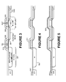
- Figures 3-7 are cross sectional views illustrating the process of manufacturing a pixel with a P + doped polysilicon pinning layer in accordance with the present invention.
- Figures 8-11 are cross sectional views illustrating an alternative process for manufacturing a pixel with a P + doped polysilicon pinning layer.
- Figure 1 shows a combination cross-sectional and schematic view of an active pixel that uses four transistors. This is known in the art as a 4T active pixel.
- a light-sensing element in this embodiment a photodiode 101, outputs a signal that is used to modulate an amplification transistor 103.
- the amplification transistor 103 is also referred to as a source follower transistor. While the light-sensing element can be one of a variety of devices, including without limitation, photogates, photodiodes, pinned photodiodes, partially pinned photodiodes, etc., in the present invention, the light-sensing element is a photodiode (whether of the pinned or partially pinned variety).
- a transfer transistor 105 is used to transfer the signal output by the photodiode 101 to a floating node 107, which is connected to the gate of the amplification transistor 103. The transfer transistor 105 is controlled by a transfer gate.
- a characteristic feature of a 4T active pixel is the presence of a transfer gate to enable true correlated double sampling (CDS). It is possible to eliminate the row select (RS) transistor in the 4T pixel to form a "4T active pixel" with just three transistors by additionally gating the supply voltage to the reset transistors. It is to be understood that this invention applies to all CMOS imagers whether they be formed with 3, 4, 5, 6, 7, or more transistors. This invention also applies to CCD image sensors.
- the photodiode 101 In operation, during an integration period (also referred to as an exposure or accumulation period), the photodiode 101 generates charge that is held in the N-type layer. After the integration period, the transfer transistor 105 is turned on to transfer the charge held in the N-type layer of the photodiode 101 to the floating node 107. After the signal has been transferred to the floating node 107, the transfer transistor 105 is turned off again for the start of a subsequent integration period.
- the signal on the floating node 107 is then used to modulate the amplification transistor 103.
- an address transistor 109 is used as a means to address the pixel and to selectively read out the signal onto a column bit line 111.
- a reset transistor 113 resets the floating node 107 to a reference voltage.
- the reference voltage is V dd . Note that while the description herein discusses the present invention in the context of a 4T pixel, the present invention may be used with a 3T, 5T, 6T, 7T or other pixel designs. In fact, the use of the present invention may be applied to any light sensing element or with either CMOS or CCD image sensors.
- Figure 1A shows a three transistor (3T) pixel design.
- the transfer transistor is omitted and the output node of the photodiode is directly connected to the amplification transistor 103.
- the reset transistor 113 is adjacent the photodiode 101 and can selectively reset the output of the photodiode to the reference voltage V dd .
- incident light 115 is incident onto the photodiode 101. However, some portion of the incident light 115 is reflected as reflected light 117. This reflected light 117 is "wasted", i.e. not sensed by the photodiode 101.
- the present invention reduces the reflection from the surface of the photodiode 101 by adding a rough polysilicon layer.
- the rough polysilicon layer may be doped with a p-type dopant.
- Such a P + doped rough polysilicon layer serves at least two purposes: (1) reduces wasted incident light and (2) acts as a P + pinning layer. Note that while the description herein shows the application of the present invention with respect to CMOS pixels, the present invention can be equally applied to CCD pixels.
- the P + doped polysilicon layer is placed close to the silicon surface and over the photodiode 101.
- the P + doped polysilicon layer can reduce reflection at the substrate/oxide boundary not only for a particular wavelength, but over a wide range of wavelengths.
- the present invention has advantages over the use of an anti-reflection coating (ARC).
- Figure 2 shows a typical 4T pixel that uses an ARC over the photodiode region.
- the ARC has a thickness that is closely correlated to a particular wavelength that is to be affected.
- the ARC and structure shown in Figure 2 are not optimized over a wide range of incident wavelengths.
- a portion of a 4T pixel is shown with a photodiode 301 formed in a p-type substrate or region.
- the pixel is bordered by a field oxide, in this example, a shallow trench isolation (STI).
- the photodiode 301 shown in Figures 3-7 is a pinned photodiode.
- the P + doped rough polysilicon layer (described below) also serves as the pinning layer.
- the transfer transistor 303 that has its transfer gate controlled by a signal TG.
- a reset transistor 305 is formed adjacent to the transfer transistor 303. The gate of the reset transistor is controlled by the signal RST.
- an insulator layer 311 is deposited.
- the insulator layer 311 is typically an oxide layer that can be formed by deposition, such as by a chemical vapor deposition or a plasma-enhanced chemical vapor deposition process. Further, the insulator layer 311 may be the same oxide layer used to form the sidewall spacers (described further below) or the oxide layer used to a resist protect oxide (RPO) used as part of a salicide process. Thus, while the insulator layer 311 may be co-functional with other oxide or dielectric layers, a dedicated insulator layer 311 is shown in Figure 3 to more clearly illustrate the present invention.
- the insulator layer 311 acts as a mask for the later formation of the P + doped polysilicon layer.
- the insulator layer 311 is patterned and masked to expose the surface of the photodiode 301. This can be done using conventional masking and etching processes.
- a polysilicon layer 501 is deposited.
- the polysilicon layer 501 in this embodiment is doped with a p-type dopant, such as boron, indium, or boron diflouride (BF 2 ).
- the doping may be done insitu with the deposition of the polysilicon layer 501, or alternatively, may be done after deposition of the polysilicon layer 501 with an ion implant process. Still alternatively, the doping may be done using a thermal diffusion process.
- the polysilicon layer 501 is a rugged polysilicon (such as that described in U.S. Patent No. 5,869,399) or a hemispherical grain (HSG) polysilicon. This provides a "rough" surface that will tend to cause less overall reflection of incident light.
- the polysilicon layer 501 need not be doped with a p-type dopant. This will result in an unpinned photodiode.
- the polysilicon layer 501 may not be doped. Instead, a separate P + pinning layer may be formed in the semiconductor substrate (such as shown in Figure 1).
- the polysilicon layer 501 can serve one of at least two purposes, and perhaps both.
- the polysilicon layer 501 may be an undoped rugged or HSG polysilicon layer, in which case it serves to minimize reflection.
- the polysilicon layer may be a p-type doped smooth polysilicon layer, in which case it serves as a P + pinning layer that allows a shallow N - region for the photodiode.
- the polysilicon layer 501 may be a P + doped rugged or HSG polysilicon layer, in which case reflections are minimized and it acts as a P + pinning layer.
- the polysilicon layer 501 is then patterned and etched so that the polysilicon layer 501 is only primarily over the photodiode 301. Note that the polysilicon layer 501 has a substantial roughness due to the use of HSG or rugged polysilicon.
- the roughness provides increased internal reflection from one grain to another grain that increases the probability of transmission to the photodiode 301.
- the roughness of the polysilicon grains can be controlled primarily through the deposition temperature.
- a second insulator layer 701 is deposited over the pixel structure to planarize and protect the underlying structure.
- FIG. 8-11 A second method of forming the structure of the present invention is shown in Figures 8-11. Specifically, as seen in Figure 8, first a spacer insulator layer 801 is deposited over the pixel structure. Then, a photoresist layer 803 having an opening 805 over the photodiode 301 is deposited.
- the spacer insulator layer 801 over the photodiode 301 is removed using the photoresist layer 803 as a mask. After the etching of the spacer insulator layer 801, the photoresist layer 803 is removed.
- a polysilicon layer 1001 is deposited over the pixel.
- the polysilicon layer 1001 is then patterned and etched to remove those portions of the polysilicon layer 1001 not over the photodiode area.
- the underlying spacer insulator layer 801 not protected by the photoresist is also etched back to form sidewall spacers.
- Figure 11 also includes a formation of a planarizing insulator layer 1101 over the pixel.
- the pixel may use p-channel transistors and the photodiode may be formed from a shallow P - region formed in an n-type substrate (or N-well).
- the pinning layer may then be formed from an N + doped polysilicon (rugged or hemispherical or smooth) layer.
- the methods and teachings of the present invention may be applied to devices of reverse polarity from that described above and shown in the drawings.
- the term rugged polysilicon is meant to encompass any type of polysilicon that has a substantially rough surface.
Landscapes
- Solid State Image Pick-Up Elements (AREA)
- Light Receiving Elements (AREA)
Abstract
Description
- The present invention relates to image sensors, and more particularly, to an image sensor that uses pixels having a polysilicon layer atop of the photodiode.
- Image sensors have become ubiquitous. They are widely used in digital still cameras, cellular phones, security cameras, medical, automobile, and other applications. The technology used to manufacture image sensors, and in particular CMOS image sensors, has continued to advance at great pace. For example, the demands of higher resolution and lower power consumption have encouraged the further miniaturization and integration of the image sensor.
- As the pixels become smaller, the surface area that can receive incident light is also reduced. The pixel typically has a light-sensing element, such as a photodiode, which receives incident light and produces a signal in relation to the amount of incident light. Because of the small size of the light-sensing element, it is important that as much incident light is captured by the light-sensing element. One major source of incident light loss occurs as a result of reflection at the photodiode (the silicon surface) to oxide (SiO2) interface. At this interface, a substantial amount of light is reflected with the consequential reduction in photodiode responsivity and quantum efficiency.
- Further, as the pixel area (and thus the photodiode area) decreases, the well capacity of the photodiode also becomes smaller. One prior art structure of a photodiode that has enhanced well capacity comprises a shallow N- region in a P-type region or substrate. A P+ pinning layer is then formed over the shallow N- region by implanting a p-type dopant (such as boron) into the shallow N- region. This structure is known as a pinned photodiode and has relatively high well capacity, but sometimes at the expense of "dark current" performance and excess "hot pixel" defects.
- In general, it is advantageous for the P+ implant to be very shallow. Having a shallow P+ surface implant enables the N- region to also be shallow. This in turn increases the capacitance of the photodiode for improved sensitivity and full well capacity and improves image lag by providing a N-implant that links up with the transfer gate in four-transistor (4T) pixel architectures.
- In a first aspect, the present invention provides a pixel according to Claim 1. Other aspects will be apparent from the attached claims.
-
- Figure 1 is a combination cross-sectional and schematic diagram of a prior art four transistor (4T) pixel which shows in detail a photodiode formed in a substrate.
- Figure 1A is a combination cross-sectional and schematic diagram of a prior art three transistor (3T) pixel which shows in detail a photodiode formed in a substrate.
- Figure 2 is a cross-sectional diagram of a 4T pixel having an anti-reflective coating (ARC).
- Figures 3-7 are cross sectional views illustrating the process of manufacturing a pixel with a P+ doped polysilicon pinning layer in accordance with the present invention.
- Figures 8-11 are cross sectional views illustrating an alternative process for manufacturing a pixel with a P+ doped polysilicon pinning layer.
- In the following description, numerous specific details are provided in order to give a thorough understanding of embodiments of the invention. One skilled in the relevant art will recognize, however, that the invention may be practiced without one or more of the specific details, or with other methods, components, materials, etc. In other instances, well known structures, materials, or operations are not shown or described in order to avoid obscuring aspects of the invention.
- Referenced throughout the specification to "one embodiment" or "an embodiment" means that a particular feature, structure, or characteristic described in connection with the embodiment and included in at least one embodiment of the present invention. Thus, the appearances of the phrase "in one embodiment" or "in an embodiment" in various places throughout the specification are not necessarily all referring to the same embodiment. Furthermore, the particular features, structures, or characteristics may be combined in any suitable manner in one or more embodiments.
- Figure 1 shows a combination cross-sectional and schematic view of an active pixel that uses four transistors. This is known in the art as a 4T active pixel. A light-sensing element, in this embodiment a
photodiode 101, outputs a signal that is used to modulate anamplification transistor 103. Theamplification transistor 103 is also referred to as a source follower transistor. While the light-sensing element can be one of a variety of devices, including without limitation, photogates, photodiodes, pinned photodiodes, partially pinned photodiodes, etc., in the present invention, the light-sensing element is a photodiode (whether of the pinned or partially pinned variety). Atransfer transistor 105 is used to transfer the signal output by thephotodiode 101 to afloating node 107, which is connected to the gate of theamplification transistor 103. Thetransfer transistor 105 is controlled by a transfer gate. - A characteristic feature of a 4T active pixel is the presence of a transfer gate to enable true correlated double sampling (CDS). It is possible to eliminate the row select (RS) transistor in the 4T pixel to form a "4T active pixel" with just three transistors by additionally gating the supply voltage to the reset transistors. It is to be understood that this invention applies to all CMOS imagers whether they be formed with 3, 4, 5, 6, 7, or more transistors. This invention also applies to CCD image sensors.
- In operation, during an integration period (also referred to as an exposure or accumulation period), the
photodiode 101 generates charge that is held in the N-type layer. After the integration period, thetransfer transistor 105 is turned on to transfer the charge held in the N-type layer of thephotodiode 101 to thefloating node 107. After the signal has been transferred to thefloating node 107, thetransfer transistor 105 is turned off again for the start of a subsequent integration period. - The signal on the
floating node 107 is then used to modulate theamplification transistor 103. Finally, anaddress transistor 109 is used as a means to address the pixel and to selectively read out the signal onto acolumn bit line 111. After readout through thecolumn bit line 111, areset transistor 113 resets thefloating node 107 to a reference voltage. In one embodiment, the reference voltage is Vdd. Note that while the description herein discusses the present invention in the context of a 4T pixel, the present invention may be used with a 3T, 5T, 6T, 7T or other pixel designs. In fact, the use of the present invention may be applied to any light sensing element or with either CMOS or CCD image sensors. - Figure 1A shows a three transistor (3T) pixel design. In this design, the transfer transistor is omitted and the output node of the photodiode is directly connected to the
amplification transistor 103. Further, thereset transistor 113 is adjacent thephotodiode 101 and can selectively reset the output of the photodiode to the reference voltage Vdd. - As can be seen in Figures 1 and 1A,
incident light 115 is incident onto thephotodiode 101. However, some portion of theincident light 115 is reflected as reflectedlight 117. Thisreflected light 117 is "wasted", i.e. not sensed by thephotodiode 101. - The present invention reduces the reflection from the surface of the
photodiode 101 by adding a rough polysilicon layer. In one embodiment, the rough polysilicon layer may be doped with a p-type dopant. Such a P+ doped rough polysilicon layer serves at least two purposes: (1) reduces wasted incident light and (2) acts as a P+ pinning layer. Note that while the description herein shows the application of the present invention with respect to CMOS pixels, the present invention can be equally applied to CCD pixels. - In one embodiment, the P+ doped polysilicon layer is placed close to the silicon surface and over the
photodiode 101. Note importantly, that the P+ doped polysilicon layer can reduce reflection at the substrate/oxide boundary not only for a particular wavelength, but over a wide range of wavelengths. Thus, the present invention has advantages over the use of an anti-reflection coating (ARC). Specifically, Figure 2 shows a typical 4T pixel that uses an ARC over the photodiode region. The ARC has a thickness that is closely correlated to a particular wavelength that is to be affected. Thus, the ARC and structure shown in Figure 2 are not optimized over a wide range of incident wavelengths. - As seen in Figure 3, a portion of a 4T pixel is shown with a
photodiode 301 formed in a p-type substrate or region. The pixel is bordered by a field oxide, in this example, a shallow trench isolation (STI). Further, thephotodiode 301 shown in Figures 3-7 is a pinned photodiode. However, it can be appreciated that the present invention can be applied to any type of light-sensing element. In the example of Figures 3-7 showing a pinned photodiode, the P+ doped rough polysilicon layer (described below) also serves as the pinning layer. Also shown in Figure 3 is thetransfer transistor 303 that has its transfer gate controlled by a signal TG. Moreover, areset transistor 305 is formed adjacent to thetransfer transistor 303. The gate of the reset transistor is controlled by the signal RST. - Still referring to Figure 3, various conventional steps are performed to form lightly doped
drain regions 307 adjacent thetransfer gate 303 and resetgate 305. Further,sidewall spacers 309 are formed on the sidewalls of the transfer and reset gates. Finally, and N+ regions are formed adjacent the transfer and reset gates to serve as the floating node and the connection to Vdd. These structures, and the steps used to form them, are conventional in the prior art, but are briefly described herein for completeness. Still, there may be additional steps, such as enhancement implants, P-well implants, and lightly doped drain (LDD) implants that are well known in the art that have been omitted to avoid obscuring the present invention. - Next, in accordance with one method of the present invention, an
insulator layer 311 is deposited. Theinsulator layer 311 is typically an oxide layer that can be formed by deposition, such as by a chemical vapor deposition or a plasma-enhanced chemical vapor deposition process. Further, theinsulator layer 311 may be the same oxide layer used to form the sidewall spacers (described further below) or the oxide layer used to a resist protect oxide (RPO) used as part of a salicide process. Thus, while theinsulator layer 311 may be co-functional with other oxide or dielectric layers, adedicated insulator layer 311 is shown in Figure 3 to more clearly illustrate the present invention. - One purpose of the
insulator layer 311 is to act as a mask for the later formation of the P+ doped polysilicon layer. Thus, as seen in Figure 4, theinsulator layer 311 is patterned and masked to expose the surface of thephotodiode 301. This can be done using conventional masking and etching processes. Further, next turning to Figure 4, apolysilicon layer 501 is deposited. Thepolysilicon layer 501 in this embodiment is doped with a p-type dopant, such as boron, indium, or boron diflouride (BF2). The doping may be done insitu with the deposition of thepolysilicon layer 501, or alternatively, may be done after deposition of thepolysilicon layer 501 with an ion implant process. Still alternatively, the doping may be done using a thermal diffusion process. In one embodiment, thepolysilicon layer 501 is a rugged polysilicon (such as that described in U.S. Patent No. 5,869,399) or a hemispherical grain (HSG) polysilicon. This provides a "rough" surface that will tend to cause less overall reflection of incident light. - It should be noted that the
polysilicon layer 501 need not be doped with a p-type dopant. This will result in an unpinned photodiode. Alternatively, thepolysilicon layer 501 may not be doped. Instead, a separate P+ pinning layer may be formed in the semiconductor substrate (such as shown in Figure 1). In short, thepolysilicon layer 501 can serve one of at least two purposes, and perhaps both. Thepolysilicon layer 501 may be an undoped rugged or HSG polysilicon layer, in which case it serves to minimize reflection. The polysilicon layer may be a p-type doped smooth polysilicon layer, in which case it serves as a P+ pinning layer that allows a shallow N- region for the photodiode. Finally, as shown in the Figures, thepolysilicon layer 501 may be a P+ doped rugged or HSG polysilicon layer, in which case reflections are minimized and it acts as a P+ pinning layer. - As seen in Figure 6, the
polysilicon layer 501 is then patterned and etched so that thepolysilicon layer 501 is only primarily over thephotodiode 301. Note that thepolysilicon layer 501 has a substantial roughness due to the use of HSG or rugged polysilicon. - As seen in Figure 7, the roughness provides increased internal reflection from one grain to another grain that increases the probability of transmission to the
photodiode 301. The roughness of the polysilicon grains can be controlled primarily through the deposition temperature. Finally, as further seen in Figure 7, asecond insulator layer 701 is deposited over the pixel structure to planarize and protect the underlying structure. - A second method of forming the structure of the present invention is shown in Figures 8-11. Specifically, as seen in Figure 8, first a
spacer insulator layer 801 is deposited over the pixel structure. Then, aphotoresist layer 803 having anopening 805 over thephotodiode 301 is deposited. - Then, at Figure 9, the
spacer insulator layer 801 over thephotodiode 301 is removed using thephotoresist layer 803 as a mask. After the etching of thespacer insulator layer 801, thephotoresist layer 803 is removed. - Next, as seen in Figure 10, a
polysilicon layer 1001 is deposited over the pixel. Thepolysilicon layer 1001 is then patterned and etched to remove those portions of thepolysilicon layer 1001 not over the photodiode area. During this patterning and etching of thepolysilicon layer 1001, the underlyingspacer insulator layer 801 not protected by the photoresist is also etched back to form sidewall spacers. The result is shown in Figure 11, which also includes a formation of aplanarizing insulator layer 1101 over the pixel. - From the foregoing, it will be appreciated that specific embodiments of the invention have been described herein for purposes of illustration, but that various modifications may be made without deviating from the spirit and scope of the invention.
- For example, it may be possible to use the concepts of the present invention with NPN pinned photodiodes, where the dopant types are switched from that shown in the Figures. Specifically, the pixel may use p-channel transistors and the photodiode may be formed from a shallow P- region formed in an n-type substrate (or N-well). The pinning layer may then be formed from an N+ doped polysilicon (rugged or hemispherical or smooth) layer. Thus, the methods and teachings of the present invention may be applied to devices of reverse polarity from that described above and shown in the drawings. Further, the term rugged polysilicon is meant to encompass any type of polysilicon that has a substantially rough surface.
- Accordingly, the invention is not limited except as by the appended claims.
Claims (43)
- A pixel comprising:a light sensitive element formed in a semiconductor substrate; anda p-type doped polysilicon layer formed atop said light sensing element.
- The pixel of Claim 1 further including:a transfer transistor formed between said light sensitive element and a floating node and selectively operative to transfer a signal from said light sensing element to said floating node; andan amplification transistor controlled by said floating node.
- The pixel of Claim 1 further including:a reset transistor formed between said light sensitive element and a node and selectively operative to reset said node to a reference voltage; andan amplification transistor controlled by said node.
- The pixel of Claim 1 wherein said light sensing element is a photodiode.
- The pixel of Claim 1 wherein said polysilicon layer is a rugged polysilicon layer.
- The pixel of Claim 1 wherein said polysilicon layer is a hemispherical grain polysilicon layer.
- The pixel of Claim 1 incorporated into a CMOS image sensor.
- The pixel of Claim 1 incorporated into a CCD image sensor.
- The pixel of Claim 1 wherein said pixel is a part of a 3T, 4T, 5T, 6T, or 7T architecture.
- The pixel of Claim 1 wherein said p-type doped polysilicon layer is doped by implantation.
- The pixel of Claim 10 wherein said implantation uses boron, indium, or boron diflouride.
- The pixel of Claim 1 wherein said p-type doped polysilicon is doped using a thermal diffusion process.
- A pixel comprising:a light sensitive element formed in a semiconductor substrate; anda rugged or hemispherical grain polysilicon layer formed atop said light sensing element.
- The pixel of Claim 13 further including:a transfer transistor formed between said light sensitive element and a floating node and selectively operative to transfer a signal from said light sensing element to said floating node; andan amplification transistor controlled by said floating node.
- The pixel of Claim 13 further including:a reset transistor formed between said light sensitive element and a node and selectively operative to reset said node to a reference voltage; andan amplification transistor controlled by said node.
- The pixel of Claim 13 wherein said light sensing element is a photodiode.
- The pixel of Claim 13 incorporated into a CMOS image sensor.
- The pixel of Claim 13 incorporated into a CCD image sensor.
- The pixel of Claim 13 wherein said pixel is a part of a 3T, 4T, 5T, 6T, or 7T architecture.
- A pixel comprising:a light sensitive element formed in a semiconductor substrate; anda p-type doped rugged or hemispherical grain polysilicon layer formed atop said light sensing element.
- The pixel of Claim 20 further including:a transfer transistor formed between said light sensitive element and a floating node and selectively operative to transfer a signal from said light sensing element to said floating node; andan amplification transistor controlled by said floating node.
- The pixel of Claim 20 further including:a reset transistor formed between said light sensitive element and a node and selectively operative to reset said node to a reference voltage; andan amplification transistor controlled by said node.
- The pixel of Claim 20 wherein said light sensing element is a photodiode.
- The pixel of Claim 20 incorporated into a CMOS image sensor.
- The pixel of Claim 20 incorporated into a CCD image sensor.
- The pixel of Claim 20 wherein said pixel is a part of a 3T, 4T, 5T, 6T, or 7T architecture.
- The pixel of Claim 20 wherein said p-type doped polysilicon layer is doped by implantation.
- The pixel of Claim 27 wherein said implantation uses boron, indium, or boron diflouride.
- The pixel of Claim 20 wherein said p-type doped polysilicon is doped using a thermal diffusion process.
- A method of forming a photodiode comprising in a p-type substrate comprising:forming a N- region in said p-type substrate; andforming a polysilicon layer over said N- region.
- The method of Claim 30 wherein said polysilicon layer is rugged polysilicon or hemispherical grain polysilicon.
- The method of Claim 30 further including:forming a transfer transistor formed between said photodiode and a floating node and selectively operative to transfer a signal from said photodiode to said floating node; andforming an amplification transistor controlled by said floating node.
- The method of Claim 30 further including:forming a reset transistor between said photodiode and a node and selectively operative to reset said node to a reference voltage; andforming an amplification transistor controlled by said node.
- The method of Claim 30 further wherein during the process of forming said polysilicon layer, a p-type dopant is used to insitu dope said polysilicon layer.
- The method of Claim 30 further including the step of doping said polysilicon layer with a p-type dopant.
- A method of forming a photodiode comprising in an n-type substrate comprising:forming a P- region in said n-type substrate; andforming a polysilicon layer over said P- region.
- The method of Claim 36 wherein said polysilicon layer is rugged polysilicon or hemispherical grain polysilicon.
- The method of Claim 36 further wherein during the process of forming said polysilicon layer, a n-type dopant is used to insitu dope said polysilicon layer.
- The method of Claim 36 further including the step of doping said polysilicon layer with a n-type dopant.
- A pixel comprising:a photodiode formed in a semiconductor substrate; andan n-type doped polysilicon layer formed atop said light sensing element.
- The pixel of Claim 40 wherein said polysilicon layer is a rugged polysilicon layer.
- A pixel comprising:a light sensitive element formed in a semiconductor substrate; andan n-type doped rugged or hemispherical grain polysilicon layer formed atop said light sensing element.
- The pixel of Claim 42 wherein said n-type doped rugged or hemispherical grain polysilicon layer is N+ doped.
Applications Claiming Priority (1)
| Application Number | Priority Date | Filing Date | Title |
|---|---|---|---|
| US11/003,298 US20060118781A1 (en) | 2004-12-03 | 2004-12-03 | Image sensor and pixel having a polysilicon layer over the photodiode |
Publications (2)
| Publication Number | Publication Date |
|---|---|
| EP1667233A2 true EP1667233A2 (en) | 2006-06-07 |
| EP1667233A3 EP1667233A3 (en) | 2009-11-18 |
Family
ID=35911176
Family Applications (1)
| Application Number | Title | Priority Date | Filing Date |
|---|---|---|---|
| EP05257097A Withdrawn EP1667233A3 (en) | 2004-12-03 | 2005-11-17 | Image sensor and pixel having a polysilicon layer over the photodiode |
Country Status (4)
| Country | Link |
|---|---|
| US (1) | US20060118781A1 (en) |
| EP (1) | EP1667233A3 (en) |
| CN (1) | CN1819277A (en) |
| TW (1) | TWI295503B (en) |
Cited By (1)
| Publication number | Priority date | Publication date | Assignee | Title |
|---|---|---|---|---|
| WO2007078719A1 (en) * | 2005-12-15 | 2007-07-12 | Micron Technology, Inc. | Light sensor having undulating features for cmos imager |
Families Citing this family (24)
| Publication number | Priority date | Publication date | Assignee | Title |
|---|---|---|---|---|
| US7442629B2 (en) | 2004-09-24 | 2008-10-28 | President & Fellows Of Harvard College | Femtosecond laser-induced formation of submicrometer spikes on a semiconductor substrate |
| US7057256B2 (en) | 2001-05-25 | 2006-06-06 | President & Fellows Of Harvard College | Silicon-based visible and near-infrared optoelectric devices |
| US7924332B2 (en) * | 2007-05-25 | 2011-04-12 | The Trustees Of The University Of Pennsylvania | Current/voltage mode image sensor with switchless active pixels |
| US8212327B2 (en) * | 2008-03-06 | 2012-07-03 | Sionyx, Inc. | High fill-factor laser-treated semiconductor device on bulk material with single side contact scheme |
| US20090302409A1 (en) * | 2008-06-04 | 2009-12-10 | Omnivision Technologies, Inc. | Image sensor with multiple thickness anti-relfective coating layers |
| US8679959B2 (en) * | 2008-09-03 | 2014-03-25 | Sionyx, Inc. | High sensitivity photodetectors, imaging arrays, and high efficiency photovoltaic devices produced using ion implantation and femtosecond laser irradiation |
| TWI382554B (en) * | 2008-10-30 | 2013-01-11 | Au Optronics Corp | Light sensing element and manufacturing method thereof |
| US8207051B2 (en) | 2009-04-28 | 2012-06-26 | Sionyx, Inc. | Semiconductor surface modification |
| JP5961332B2 (en) * | 2009-09-17 | 2016-08-02 | サイオニクス、エルエルシー | Photosensitive imaging device and related method |
| US9673243B2 (en) | 2009-09-17 | 2017-06-06 | Sionyx, Llc | Photosensitive imaging devices and associated methods |
| US9911781B2 (en) | 2009-09-17 | 2018-03-06 | Sionyx, Llc | Photosensitive imaging devices and associated methods |
| US8692198B2 (en) | 2010-04-21 | 2014-04-08 | Sionyx, Inc. | Photosensitive imaging devices and associated methods |
| WO2011160130A2 (en) | 2010-06-18 | 2011-12-22 | Sionyx, Inc | High speed photosensitive devices and associated methods |
| CN105679862A (en) | 2010-12-21 | 2016-06-15 | 西奥尼克斯公司 | Semiconductor devices having reduced substrate damage and associated methods |
| US8861909B2 (en) | 2011-02-17 | 2014-10-14 | Cornell University | Polysilicon photodetector, methods and applications |
| KR101833269B1 (en) | 2011-03-10 | 2018-02-28 | 사이오닉스, 엘엘씨 | Three dimensional sensors, systems, and associated methods |
| US9496308B2 (en) | 2011-06-09 | 2016-11-15 | Sionyx, Llc | Process module for increasing the response of backside illuminated photosensitive imagers and associated methods |
| US20130016203A1 (en) | 2011-07-13 | 2013-01-17 | Saylor Stephen D | Biometric imaging devices and associated methods |
| US8865507B2 (en) | 2011-09-16 | 2014-10-21 | Sionyx, Inc. | Integrated visible and infrared imager devices and associated methods |
| US9064764B2 (en) | 2012-03-22 | 2015-06-23 | Sionyx, Inc. | Pixel isolation elements, devices, and associated methods |
| JP6466346B2 (en) | 2013-02-15 | 2019-02-06 | サイオニクス、エルエルシー | High dynamic range CMOS image sensor with anti-blooming characteristics and associated method |
| WO2014151093A1 (en) | 2013-03-15 | 2014-09-25 | Sionyx, Inc. | Three dimensional imaging utilizing stacked imager devices and associated methods |
| WO2014209421A1 (en) | 2013-06-29 | 2014-12-31 | Sionyx, Inc. | Shallow trench textured regions and associated methods |
| CN108346674B (en) * | 2018-01-30 | 2019-01-18 | 武汉新芯集成电路制造有限公司 | Preparation method, silicon wafer and the imaging sensor of semiconductor wafers |
Citations (1)
| Publication number | Priority date | Publication date | Assignee | Title |
|---|---|---|---|---|
| US5869399A (en) | 1997-08-07 | 1999-02-09 | Mosel Vitelic Inc. | Method for increasing utilizable surface of rugged polysilicon layer in semiconductor device |
Family Cites Families (11)
| Publication number | Priority date | Publication date | Assignee | Title |
|---|---|---|---|---|
| JP3006539B2 (en) * | 1997-05-12 | 2000-02-07 | 日本電気株式会社 | Method for manufacturing semiconductor device |
| US6232626B1 (en) * | 1999-02-01 | 2001-05-15 | Micron Technology, Inc. | Trench photosensor for a CMOS imager |
| US6376868B1 (en) * | 1999-06-15 | 2002-04-23 | Micron Technology, Inc. | Multi-layered gate for a CMOS imager |
| US6310366B1 (en) * | 1999-06-16 | 2001-10-30 | Micron Technology, Inc. | Retrograde well structure for a CMOS imager |
| US6291289B2 (en) * | 1999-06-25 | 2001-09-18 | Micron Technology, Inc. | Method of forming DRAM trench capacitor with metal layer over hemispherical grain polysilicon |
| JP3782297B2 (en) * | 2000-03-28 | 2006-06-07 | 株式会社東芝 | Solid-state imaging device and manufacturing method thereof |
| US6504196B1 (en) * | 2001-08-30 | 2003-01-07 | Micron Technology, Inc. | CMOS imager and method of formation |
| KR20030057677A (en) * | 2001-12-29 | 2003-07-07 | 주식회사 하이닉스반도체 | Image sensor with improved charge capacity and fabricating method of the same |
| KR100462164B1 (en) * | 2002-01-11 | 2004-12-17 | 매그나칩 반도체 유한회사 | Cmos image sensor with enhanced fill factor |
| US6723613B2 (en) * | 2002-07-02 | 2004-04-20 | Semiconductor Manufacturing International (Shanghai) Corporation | Method of forming an isolated-grain rugged polysilicon surface via a temperature ramping step |
| US6847051B2 (en) * | 2003-05-23 | 2005-01-25 | Micron Technology, Inc. | Elevated photodiode in an image sensor |
-
2004
- 2004-12-03 US US11/003,298 patent/US20060118781A1/en not_active Abandoned
-
2005
- 2005-11-02 TW TW094138470A patent/TWI295503B/en not_active IP Right Cessation
- 2005-11-17 EP EP05257097A patent/EP1667233A3/en not_active Withdrawn
- 2005-12-01 CN CN200510126605.6A patent/CN1819277A/en active Pending
Patent Citations (1)
| Publication number | Priority date | Publication date | Assignee | Title |
|---|---|---|---|---|
| US5869399A (en) | 1997-08-07 | 1999-02-09 | Mosel Vitelic Inc. | Method for increasing utilizable surface of rugged polysilicon layer in semiconductor device |
Cited By (2)
| Publication number | Priority date | Publication date | Assignee | Title |
|---|---|---|---|---|
| WO2007078719A1 (en) * | 2005-12-15 | 2007-07-12 | Micron Technology, Inc. | Light sensor having undulating features for cmos imager |
| US7456452B2 (en) | 2005-12-15 | 2008-11-25 | Micron Technology, Inc. | Light sensor having undulating features for CMOS imager |
Also Published As
| Publication number | Publication date |
|---|---|
| US20060118781A1 (en) | 2006-06-08 |
| TWI295503B (en) | 2008-04-01 |
| TW200620645A (en) | 2006-06-16 |
| CN1819277A (en) | 2006-08-16 |
| EP1667233A3 (en) | 2009-11-18 |
Similar Documents
| Publication | Publication Date | Title |
|---|---|---|
| US20060118781A1 (en) | Image sensor and pixel having a polysilicon layer over the photodiode | |
| US6974715B2 (en) | Method for manufacturing CMOS image sensor using spacer etching barrier film | |
| EP1655780B1 (en) | Image sensor and pixel having an anti-reflective coating over the photodiode | |
| US7217967B2 (en) | CMOS image sensor and method for manufacturing the same | |
| US12289924B2 (en) | Transistors having increased effective channel width | |
| US7524695B2 (en) | Image sensor and pixel having an optimized floating diffusion | |
| KR100794873B1 (en) | Custom Gate Work Functions for Image Sensors | |
| US7888215B2 (en) | CMOS image sensor with high full-well-capacity | |
| KR20080057356A (en) | Imaging with Gate-Controlled Charge Storage | |
| US20030062561A1 (en) | Alternate method for photodiode formation in CMOS image sensors | |
| CN113451341A (en) | Transistor with increased effective channel width | |
| US20080042176A1 (en) | Method for making image sensor with reduced etching damage | |
| US8129765B2 (en) | CMOS image sensor with photo-detector protecting layers | |
| EP1681721B1 (en) | Image sensor pixel having a lateral doping profile formed with indium doping | |
| US20060284223A1 (en) | CMOS image sensor and manufacturing method thereof | |
| US20080157256A1 (en) | Cmos image sensor and method of manufacturing thereof | |
| US7534643B2 (en) | CMOS image sensor and method for fabricating the same | |
| KR102935218B1 (en) | Image sensor | |
| US7459332B2 (en) | CMOS image sensor and method for manufacturing the same | |
| KR20070034292A (en) | CMOS image sensor and its manufacturing method |
Legal Events
| Date | Code | Title | Description |
|---|---|---|---|
| PUAI | Public reference made under article 153(3) epc to a published international application that has entered the european phase |
Free format text: ORIGINAL CODE: 0009012 |
|
| 17P | Request for examination filed |
Effective date: 20051206 |
|
| AK | Designated contracting states |
Kind code of ref document: A2 Designated state(s): AT BE BG CH CY CZ DE DK EE ES FI FR GB GR HU IE IS IT LI LT LU LV MC NL PL PT RO SE SI SK TR |
|
| AX | Request for extension of the european patent |
Extension state: AL BA HR MK YU |
|
| PUAL | Search report despatched |
Free format text: ORIGINAL CODE: 0009013 |
|
| AK | Designated contracting states |
Kind code of ref document: A3 Designated state(s): AT BE BG CH CY CZ DE DK EE ES FI FR GB GR HU IE IS IT LI LT LU LV MC NL PL PT RO SE SI SK TR |
|
| AX | Request for extension of the european patent |
Extension state: AL BA HR MK YU |
|
| AKX | Designation fees paid |
Designated state(s): AT BE BG CH CY CZ DE DK EE ES FI FR GB GR HU IE IS IT LI LT LU LV MC NL PL PT RO SE SI SK TR |
|
| STAA | Information on the status of an ep patent application or granted ep patent |
Free format text: STATUS: THE APPLICATION IS DEEMED TO BE WITHDRAWN |
|
| 18D | Application deemed to be withdrawn |
Effective date: 20100519 |