EP1666645A1 - Silicon carbide product, method for producing same, and method for cleaning silicon carbide product - Google Patents
Silicon carbide product, method for producing same, and method for cleaning silicon carbide product Download PDFInfo
- Publication number
- EP1666645A1 EP1666645A1 EP04747456A EP04747456A EP1666645A1 EP 1666645 A1 EP1666645 A1 EP 1666645A1 EP 04747456 A EP04747456 A EP 04747456A EP 04747456 A EP04747456 A EP 04747456A EP 1666645 A1 EP1666645 A1 EP 1666645A1
- Authority
- EP
- European Patent Office
- Prior art keywords
- silicon carbide
- cleaning
- acid
- carbide product
- semiconductor device
- Prior art date
- Legal status (The legal status is an assumption and is not a legal conclusion. Google has not performed a legal analysis and makes no representation as to the accuracy of the status listed.)
- Granted
Links
Images





Classifications
-
- C—CHEMISTRY; METALLURGY
- C30—CRYSTAL GROWTH
- C30B—SINGLE-CRYSTAL GROWTH; UNIDIRECTIONAL SOLIDIFICATION OF EUTECTIC MATERIAL OR UNIDIRECTIONAL DEMIXING OF EUTECTOID MATERIAL; REFINING BY ZONE-MELTING OF MATERIAL; PRODUCTION OF A HOMOGENEOUS POLYCRYSTALLINE MATERIAL WITH DEFINED STRUCTURE; SINGLE CRYSTALS OR HOMOGENEOUS POLYCRYSTALLINE MATERIAL WITH DEFINED STRUCTURE; AFTER-TREATMENT OF SINGLE CRYSTALS OR A HOMOGENEOUS POLYCRYSTALLINE MATERIAL WITH DEFINED STRUCTURE; APPARATUS THEREFOR
- C30B29/00—Single crystals or homogeneous polycrystalline material with defined structure characterised by the material or by their shape
- C30B29/10—Inorganic compounds or compositions
- C30B29/36—Carbides
-
- H—ELECTRICITY
- H10—SEMICONDUCTOR DEVICES; ELECTRIC SOLID-STATE DEVICES NOT OTHERWISE PROVIDED FOR
- H10P—GENERIC PROCESSES OR APPARATUS FOR THE MANUFACTURE OR TREATMENT OF DEVICES COVERED BY CLASS H10
- H10P14/00—Formation of materials, e.g. in the shape of layers or pillars
- H10P14/20—Formation of materials, e.g. in the shape of layers or pillars of semiconductor materials
- H10P14/29—Formation of materials, e.g. in the shape of layers or pillars of semiconductor materials characterised by the substrates
- H10P14/2901—Materials
- H10P14/2902—Materials being Group IVA materials
- H10P14/2904—Silicon carbide
-
- H—ELECTRICITY
- H10—SEMICONDUCTOR DEVICES; ELECTRIC SOLID-STATE DEVICES NOT OTHERWISE PROVIDED FOR
- H10D—INORGANIC ELECTRIC SEMICONDUCTOR DEVICES
- H10D62/00—Semiconductor bodies, or regions thereof, of devices having potential barriers
- H10D62/80—Semiconductor bodies, or regions thereof, of devices having potential barriers characterised by the materials
- H10D62/83—Semiconductor bodies, or regions thereof, of devices having potential barriers characterised by the materials being Group IV materials, e.g. B-doped Si or undoped Ge
- H10D62/832—Semiconductor bodies, or regions thereof, of devices having potential barriers characterised by the materials being Group IV materials, e.g. B-doped Si or undoped Ge being Group IV materials comprising two or more elements, e.g. SiGe
- H10D62/8325—Silicon carbide
-
- H—ELECTRICITY
- H10—SEMICONDUCTOR DEVICES; ELECTRIC SOLID-STATE DEVICES NOT OTHERWISE PROVIDED FOR
- H10P—GENERIC PROCESSES OR APPARATUS FOR THE MANUFACTURE OR TREATMENT OF DEVICES COVERED BY CLASS H10
- H10P14/00—Formation of materials, e.g. in the shape of layers or pillars
- H10P14/60—Formation of materials, e.g. in the shape of layers or pillars of insulating materials
- H10P14/69—Inorganic materials
- H10P14/6903—Inorganic materials containing silicon
- H10P14/6905—Inorganic materials containing silicon being a silicon carbide or silicon carbonitride and not containing oxygen, e.g. SiC or SiC:H
-
- H—ELECTRICITY
- H10—SEMICONDUCTOR DEVICES; ELECTRIC SOLID-STATE DEVICES NOT OTHERWISE PROVIDED FOR
- H10P—GENERIC PROCESSES OR APPARATUS FOR THE MANUFACTURE OR TREATMENT OF DEVICES COVERED BY CLASS H10
- H10P70/00—Cleaning of wafers, substrates or parts of devices
- H10P70/10—Cleaning before device manufacture, i.e. Begin-Of-Line process
- H10P70/15—Cleaning before device manufacture, i.e. Begin-Of-Line process by wet cleaning only
-
- Y—GENERAL TAGGING OF NEW TECHNOLOGICAL DEVELOPMENTS; GENERAL TAGGING OF CROSS-SECTIONAL TECHNOLOGIES SPANNING OVER SEVERAL SECTIONS OF THE IPC; TECHNICAL SUBJECTS COVERED BY FORMER USPC CROSS-REFERENCE ART COLLECTIONS [XRACs] AND DIGESTS
- Y10—TECHNICAL SUBJECTS COVERED BY FORMER USPC
- Y10T—TECHNICAL SUBJECTS COVERED BY FORMER US CLASSIFICATION
- Y10T428/00—Stock material or miscellaneous articles
- Y10T428/31—Surface property or characteristic of web, sheet or block
Definitions
- This invention relates to a silicon carbide product and, in particular, relates to silicon carbide for use in a semiconductor device or a structure, such as a member for manufacturing a semiconductor device and a method of manufacturing such silicon carbide.
- silicon carbide has excellent heat resistance and thus is used as a member for manufacturing a semiconductor device, such as a furnace core tube, a liner tube, a carrying tray, or a wafer boat. Further, it is known that silicon carbide forms a semiconductor device itself by the use of its semiconductor-like properties.
- JP-A Japanese Unexamined Patent Application Publication
- reference document 1 Japanese Unexamined Patent Application Publication
- JP-A Japanese Unexamined Patent Application Publication
- H11-8216 proposes that a member for manufacturing a semiconductor device is made of silicon carbide be subjected to a heat treatment in a high temperature oxygen atmosphere to thereby form a silicon oxide film at the surface thereof and then the silicon oxide film at the surface is dissolved and removed by hydrofluoric acid. Further, reference documents 1 and 2 respectively disclose that silicon carbide is cleaned with dilute hydrofluoric acid (HF 7%) and that cleaning with dilute HF (HF 5%) is carried out after oxidizing the surface.
- HF 7% dilute hydrofluoric acid
- HF 5% cleaning with dilute HF
- JP-A Japanese Unexamined Patent Application Publication
- reference document 3 discloses a method of forming a field-effect transistor.
- the electron mobility can be improved by forming a gate insulating film of a field-effect transistor on a silicon carbide region and then applying a heat treatment at a temperature in the range of 900 to 1000°C in an atmosphere containing water for a predetermined time.
- reference document 3 also describes carrying out cleaning with dilute HF before the growth of the gate oxide film or the like, or carrying out RCA cleaning that combines NH 4 OH+H 2 O 2 and HCl+H 2 O 2 .
- reference documents 1 to 3 only disclose cleaning the silicon carbide and discuss nothing about the surface condition of the silicon carbide after the cleaning. In other words, these reference documents 1 to 3 disclose nothing about the kind of impurities remaining on the surface of the silicon carbide after the cleaning according to the normal technique and the impurity concentration thereof. Further, although reduction in contamination and defect is essential for forming a semiconductor element by the use of silicon carbide, reference documents 1 to 3 suggest nothing about an optimal value of contamination amount etc. on silicon carbide or a contamination amount adjusting method and, therefore, under the circumstances, it is difficult to realize the theoretical properties of silicon carbide.
- a silicon carbide product which has a surface with a metal impurity concentration of 1 ⁇ 10 11 (atoms/cm 2 ) or less.
- a method of cleaning a silicon carbide product which includes the step of immersing silicon carbide in an acid to reduce surface metal impurities to 1 ⁇ 10 11 (atoms/cm 2 ) or less.
- a method of manufacturing silicon carbide product which includes the step of comprising a process of cleaning silicon carbide with an acid to reduce surface metal impurities to 1 ⁇ 10 11 (atoms/cm 2 ) or less.
- a silicon carbide or silicon semiconductor device such as a field-effect transistor or the like is adversely affected by the impurity concentration on the surface of silicon carbide and therefore cannot achieve the theoretical properties.
- this invention provides an impurity concentration on the surface of silicon carbide that can eliminate the adverse influence and a cleaning method that can realize such an impurity concentration.
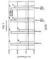
- Fig. 1 there are shown impurity (Fe) concentrations before and after cleaning in the case where silicon carbide is cleaned according to conventional cleaning methods.
- the axis of ordinates is given graduations of 1.E+00; 1.E+01; 1.E+02; and 1.E+03 in terms of ( ⁇ 10 10 atoms/cm 2 ) and these graduations respectively show concentrations of 1; 1 ⁇ 10 1 ; 1 ⁇ 10 2 ; and 1 ⁇ 10 3 with respect to ( ⁇ 10 10 atoms/cm 2 ).
- dilute HF (0.5%) cleaning or RCA cleaning that combines NH 4 OH+H 2 O 2 and HCl+H 2 O 2 is carried out before the growth of the gate oxide film, but the impurity concentration cannot be reduced to the foregoing 1 ⁇ 0 11 (atoms/cm 2 ) or less even by the RCA cleaning.
- This invention makes it clear that surface metal impurities including iron can be removed to 1x10 11 (atoms/cm 2 ) or less by cleaning silicon carbide by the use of hydrofluoric acid or hydrochloric acid having a predetermined or more concentration or by the use of a liquid containing sulfuric acid and a hydrogen peroxide solution.
- Table 2 below shows cleaning solutions and the iron removal ratios when silicon carbide (SiC) is cleaned with the respective cleaning solutions, along with the cleaning conditions.
- the iron removal ratio is calculated in terms of 100 - (after-cleaning impurities (atoms/cm 2 ) / before-cleaning impurities (atoms/cm 2 )) ⁇ 100.
- SPM cleaning solution
- HPF hydrogen peroxide solution
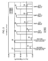
- Fig. 2 shows the Fe removal effects of the respective cleaning solutions on the surface of the silicon carbide corresponding to Table 2.
- Fe on the surface of the silicon carbide can be reduced to 1 ⁇ 10 11 (atoms/cm 2 ) or less by the cleaning using each of the foregoing cleaning solutions.
- the aqueous solution containing sulfuric acid (97%) and hydrogen peroxide (30%), among the foregoing cleaning solutions, is particularly excellent in Fe removal effect.
- Table 3 show the results of an experiment by the use of a metal impurity segregation evaluation apparatus.
- measurement is made of impurity distributions after putting a solution containing Fe, Ni, and Cu on a curved silicon carbide (SiC) wafer and segregating them, and impurity distributions after cleaning the impurity-segregated wafer by the cleaning method according to this invention.
- the cleaning is carried out using an aqueous solution (SPM) with a pH of 4 or less containing sulfuric acid (97%) and a hydrogen peroxide solution (30%) and the Fe, Ni, and Cu removal effects on the surface of silicon carbide after the cleaning are shown in association with distances from the center of the curved wafer.
- SPM aqueous solution
- Table 6 shows changes in the number of atoms of the respective components before and after the cleaning at the center of the surface of the silicon carbide. As clear from these tables, it is understood that Fe, Ni, and Cu remain only by 0.3, 0.2, and 0.16 (atoms/cm 2 ), respectively, on the surface of the silicon carbide cleaned by the SPM even at the curve center where the segregation reaches the largest amounts.
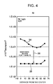
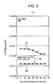
- Figs. 3, 4, and 5 respectively correspond to Tables 3, 4, and 5 and show the concentrations (atoms/cm 2 ) of Fe, Ni, and Cu on the surface of the silicon carbide.
- Figs. 3 to 5 show the Fe, Ni, and Cu removal effects after the cleaning with the aqueous solution (SPM) containing sulfuric acid (97%) and the hydrogen peroxide solution (30%), wherein the axis of abscissas represents distance from the center of the silicon carbide.
- SPM aqueous solution
- HPM hydrogen peroxide solution
- Fig. 6 there are shown changes of the impurities Fe, Ni, and Cu at the center of the surface of the silicon carbide when the silicon carbide is cleaned by the use of the aqueous solution containing sulfuric acid (97%) and the hydrogen peroxide solution (30%). It is understood that Fe, Ni, and Cu, which were each 1 ⁇ 10 12 (atoms/cm 2 ) or more before the cleaning as indicated by reference numeral 21, each have reached 1 ⁇ 10 11 (atoms/cm 2 ) or less after the cleaning as indicated by reference numeral 22.
- a method according to the first example of this invention is applicable to the manufacture of a field-effect transistor (hereinafter abbreviated as MOSFET) having a gate, a source, and a drain.
- MOSFET field-effect transistor
- SiC silicon carbide
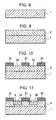
- Fig. 7 is a flowchart of fabricating a MOSFET using a silicon carbide substrate and Fig. 8 to Fig. 14 are sectional views showing, in sequence, the fabrication processes of the MOSFET using the silicon carbide substrate.
- a p-type 4H-SiC (0001) substrate 1 was prepared as silicon carbide and cleaning according to this invention was carried out before growing a p-type epitaxial layer on the surface of the silicon carbide substrate 1 (Fig. 7, step SA1).
- the cleaning method was such that sulfuric acid (97%) and a hydrogen peroxide solution (30%) were mixed in a volume ratio of 4:1 and the silicon carbide substrate 1 was immersed in this chemical solution for 10 minutes. After the immersion, the silicon carbide substrate 1 was rinsed with pure water for 10 minutes and dried with nitrogen blow.
- a p-type epitaxial layer 2 was grown after the cleaning (Fig. 7, step SA2).
- the silicon carbide substrate 1 having the p-type epitaxial layer 2 was immersed for 10 minutes in a chemical solution in the form of an aqueous solution obtained by mixing sulfuric acid (97%) and a hydrogen peroxide solution (30%) in a volume ratio of 4:1 (Fig. 7, step SA3). Subsequently, after the immersion, the substrate 1 with the epitaxial layer 2 was rinsed with pure water for 10 minutes and dried with nitrogen blow.
- source and drain regions were opened in a resist 3c by the photolithography process, thereby forming a source region opening portion 3a and a drain region opening portion 3b (Fig. 7, step SA4). Note that the resist 3c was actually continuous in a region other than the opening portions 3a and 3b.
- a gate region was opened in the oxide films 5a and 5b by a photolithography process, thereby forming a gate region opening portion 5c (Fig. 7, step SA6).
- the oxide films 5a and 5b were continuously formed at a portion other than the gate region opening portion 5c.
- the foregoing cleaning according to this invention was carried out before deposition of a gate oxide film.
- the cleaning method was the same as that described before, i.e. the substrate shown in Fig. 12 was immersed for 10 minutes in a cleaning solution obtained by mixing sulfuric acid (97%) and a hydrogen peroxide solution (30%) in a volume ratio of 4:1 (Fig. 7, step SA7). After the immersion, the substrate was rinsed with pure water for 10 minutes and dried with nitrogen blow.
- a gate oxide film 6 was formed by thermal oxidation (Fig. 7, step SA8).
- step SA9 After the formation of the gate oxide film 6, as shown in Fig. 14, electrodes 7a, 7b, and 7c were formed, thereby fabricating a MOSFET (step SA9).
- the oxide films 5a and 5b were continuously formed at a portion other than the electrodes 7a, 7b, and 7c, i.e. at a portion other than the opening portions 5c, 5d, and 5e.
- an electrode material usable in the MOSFET it may be any of a metal film of Al, Mo, or the like, a silicide film of W-Si 2 , Mo-Si 2 , Ti-Si 2 , or the like, and an n- or p-type silicon gate electrode.
- Hydrofluoric acid (45% or more) or HCl (35% or more) may be used as a cleaning solution instead of the liquid containing sulfuric acid and the hydrogen peroxide solution.
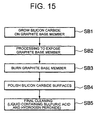
- Fig. 15 is a flowchart of fabricating silicon carbide dummy wafers and Fig. 16 to Fig. 19 are diagrams showing the fabrication processes of the silicon carbide dummy wafers in sequence.
- a disk-shaped graphite base member 11 was first prepared and, then, as shown in Fig. 17, a silicon carbide 12 was grown by a CVD method so as to cover all surfaces of the graphite base member 11 (Fig. 15, step SB1).
- the processing was performed to remove side portions of the silicon carbide 12 so that the graphite base member 11 was exposed (Fig. 15, step SB2).
- the graphite base member 11 having the silicon carbides 12a and 12a formed on its both surfaces was burned in an oxygen atmosphere, thereby separating the silicon carbide wafers (Fig. 15, step SB3).
- the surfaces of the remaining silicon carbide wafers 12a and 12b were polished (step SB4).
- the silicon carbide wafers were immersed for 10 minutes in a chemical solution (cleaning solution) according to this invention obtained by mixing sulfuric acid (97%) and a hydrogen peroxide solution (30%) in a volume ratio of 4:1 (Fig. 15, step SB5).
- cleaning solution obtained by mixing sulfuric acid (97%) and a hydrogen peroxide solution (30%) in a volume ratio of 4:1.
- the wafers were rinsed with pure water for 10 minutes and dried with nitrogen blow, thereby fabricating the polycrystal silicon carbide wafers.
- silicon carbide having high cleanliness can be obtained and, as a result, it becomes possible to obtain a semiconductor device with no need to consider degradation of the properties etc. due to impurities.
- this invention when applied to a semiconductor manufacturing member or the like, is advantageous in that it is also possible to prevent an adverse influence to a processing object caused by scattering of impurities, and so on.
- the cleaning method according to this invention is applied to the manufacture of the semiconductor device.
- this invention is by no means limited thereto and is also applicable to semiconductor manufacturing members such as a diffusion furnace, and other structures. Further, this invention is also applicable to a surface treatment of a member formed with a silicon carbide thin film, and so on.
Landscapes
- Chemical & Material Sciences (AREA)
- Inorganic Chemistry (AREA)
- Engineering & Computer Science (AREA)
- Crystallography & Structural Chemistry (AREA)
- Materials Engineering (AREA)
- Metallurgy (AREA)
- Organic Chemistry (AREA)
- Cleaning Or Drying Semiconductors (AREA)
- Crystals, And After-Treatments Of Crystals (AREA)
- Insulated Gate Type Field-Effect Transistor (AREA)
Abstract
Description
- This invention relates to a silicon carbide product and, in particular, relates to silicon carbide for use in a semiconductor device or a structure, such as a member for manufacturing a semiconductor device and a method of manufacturing such silicon carbide.
- Generally, silicon carbide has excellent heat resistance and thus is used as a member for manufacturing a semiconductor device, such as a furnace core tube, a liner tube, a carrying tray, or a wafer boat. Further, it is known that silicon carbide forms a semiconductor device itself by the use of its semiconductor-like properties.
- When silicon carbide is used as a member for manufacturing semiconductor device, it is necessary to prevent contamination of a semiconductor wafer or the like processed by such a member. Therefore, the silicon carbide forming the semiconductor device manufacturing member is periodically cleaned with hydrofluoric acid, pure water, or the like. In order to stably carry out such periodic cleaning in a short time, Japanese Unexamined Patent Application Publication (JP-A) No. H06-128036 (hereinafter referred to as reference document 1) proposes that the surface roughness, Rmax, of a silicon carbide member for manufacturing a semiconductor device be set to 3.2S or less. On the other hand, Japanese Unexamined Patent Application Publication (JP-A) No. H11-8216 (hereinafter referred to as reference document 2) proposes that a member for manufacturing a semiconductor device is made of silicon carbide be subjected to a heat treatment in a high temperature oxygen atmosphere to thereby form a silicon oxide film at the surface thereof and then the silicon oxide film at the surface is dissolved and removed by hydrofluoric acid. Further,
reference documents HF 5%) is carried out after oxidizing the surface. - Further, as a method of forming a semiconductor device by the use of silicon carbide, Japanese Unexamined Patent Application Publication (JP-A) No. 2003-86792 (hereinafter referred to as reference document 3) discloses a method of forming a field-effect transistor. Specifically, reference document 3 points out that the electron mobility can be improved by forming a gate insulating film of a field-effect transistor on a silicon carbide region and then applying a heat treatment at a temperature in the range of 900 to 1000°C in an atmosphere containing water for a predetermined time. Further, reference document 3 also describes carrying out cleaning with dilute HF before the growth of the gate oxide film or the like, or carrying out RCA cleaning that combines NH4OH+H2O2 and HCl+H2O2.
- However,
reference documents 1 to 3 only disclose cleaning the silicon carbide and discuss nothing about the surface condition of the silicon carbide after the cleaning. In other words, thesereference documents 1 to 3 disclose nothing about the kind of impurities remaining on the surface of the silicon carbide after the cleaning according to the normal technique and the impurity concentration thereof. Further, although reduction in contamination and defect is essential for forming a semiconductor element by the use of silicon carbide,reference documents 1 to 3 suggest nothing about an optimal value of contamination amount etc. on silicon carbide or a contamination amount adjusting method and, therefore, under the circumstances, it is difficult to realize the theoretical properties of silicon carbide. - Therefore, it is an object of this invention to provide silicon carbide suitable for a semiconductor device or a member for manufacturing the semiconductor device.
- It is another object of this invention to provide a cleaning method for obtaining the foregoing silicon carbide.
- It is still another object of this invention to provide a product using silicon carbide with a low impurity concentration.
- According to one aspect of this invention, there is provided a silicon carbide product which has a surface with a metal impurity concentration of 1×10¹¹ (atoms/cm2) or less.
- Further, according to another aspect of this invention, there is provided obtained a method of cleaning a silicon carbide product which includes the step of immersing silicon carbide in an acid to reduce surface metal impurities to 1×10¹¹ (atoms/cm2) or less.
- Further, according to still another aspect of this invention, there is provided a method of manufacturing silicon carbide product which includes the step of comprising a process of cleaning silicon carbide with an acid to reduce surface metal impurities to 1×10¹¹ (atoms/cm2) or less.
-
- Fig. 1 is a diagram showing evaluation results of cleaning according to conventional silicon carbide cleaning methods;
- Fig. 2 is a diagram showing Fe removal effects on the surface of silicon carbide according to cleaning methods of this invention;
- Fig. 3 is a diagram showing an Fe removal effect on silicon carbide by the use of an aqueous solution (SPM) containing sulfuric acid (97%) and hydrogen peroxide (30%) which is used in this invention;
- Fig. 4 is a diagram showing an Ni removal effect on the silicon carbide by the use of the aqueous solution (SPM) used in Fig. 3;
- Fig. 5 is a diagram showing a Cu removal effect on the silicon carbide by the use of the aqueous solution (SPM) used in Figs. 3 and 4;
- Fig. 6 is a diagram for explaining the effect of this invention when the silicon carbide is cleaned by the use of the aqueous solution (SPM) containing sulfuric acid (97%) and hydrogen peroxide (30%);
- Fig. 7 is a flowchart showing the case where this invention is applied to the fabrication of a MOSFET having a silicon carbide substrate;
- Fig. 8 is a sectional view showing a process of fabricating the MOSFET according to the flowchart of Fig. 7;
- Fig. 9 is a sectional view showing a process performed subsequently to the process shown in Fig. 8;
- Fig. 10 is a sectional view showing a process performed after the process shown in Fig. 9;
- Fig. 11 is a sectional view for explaining a process performed next to the process shown in Fig. 10;
- Fig. 12 is a sectional view for explaining a process performed after the process shown in Fig. 11;
- Fig. 13 is a sectional view showing a post-process of Fig. 12;
- Fig. 14 is a sectional view showing a process performed after the process shown in Fig. 13;
- Fig. 15 is a flowchart for explaining the case where a silicon carbide dummy wafer is fabricated by the use of this invention;
- Fig. 16 is a diagram showing a process of fabricating the silicon carbide dummy wafer according to the flowchart shown in Fig. 15;
- Fig. 17 is a diagram for explaining a process performed after the process shown in Fig. 16;
- Fig. 18 is a diagram showing a process performed subsequently to the process shown in Fig. 17; and
- Fig. 19 is a diagram showing a final process of the silicon carbide dummy wafer fabrication processes.
- At first, the circumstances of this invention will be described.
- According to knowledge of the present inventors, it often occurs that the theoretical properties of silicon carbide are not obtained in a semiconductor device using the silicon carbide and that the theoretical properties are not obtained also in a semiconductor device of silicon or the like manufactured by using a semiconductor device manufacturing silicon carbide member, and it has been found that such variation in properties is caused by the metal impurity concentration on the surface of the silicon carbide.
- Particularly, a silicon carbide or silicon semiconductor device such as a field-effect transistor or the like is adversely affected by the impurity concentration on the surface of silicon carbide and therefore cannot achieve the theoretical properties.
- Based on such knowledge, this invention provides an impurity concentration on the surface of silicon carbide that can eliminate the adverse influence and a cleaning method that can realize such an impurity concentration.
- Specifically, according to experiments by the present inventors, it has been found that mainly iron (Fe) and an iron alloy remain as impurities on the surface of silicon carbide even if cleaned and that when the concentration of those impurities is 1×10¹¹ (atoms/cm2) or less, there is obtained a suitable semiconductor device having the properties quite close to the theoretical value.
- Referring here to Fig. 1, there are shown impurity (Fe) concentrations before and after cleaning in the case where silicon carbide is cleaned according to conventional cleaning methods. Herein, the axis of ordinates is given graduations of 1.E+00; 1.E+01; 1.E+02; and 1.E+03 in terms of (×1010 atoms/cm2) and these graduations respectively show concentrations of 1; 1×101; 1×10²; and 1×10³ with respect to (×1010 atoms/cm2). On the other hand, on the axis of abscissas, two cleaning results using HCl+H2O2 according to the conventional cleaning method and two
cleaning results 26 using hydrofluoric acid (0.5%) according to the conventional cleaning method are shown along withimpurity concentrations 25 before the cleaning. Table 1 below shows the removal ratios of iron along with the contents of cleaning when such cleaning is carried out on silicon carbide (SiC). As shown in Table 1 below and Fig. 1, it is understood that the concentrations of the metal impurities (iron or iron compound) according to the conventional cleaning methods are far larger than 1×10¹¹ (atoms/cm2) found in this invention.Table 1 Iron Removal Ratios on SiC for Respective Chemical Solutions Before Clean- After Cleaning Removal Ratio (%) 100-After Cleaning/ Before Cleaning ×100 Cleaning Solution Cleaning Contents ×1010 atmos/cm2 609 52 91 HCl+H2O2 HPM (HCI: H2O2 : H2O=1:1:6 92°C)for 10 minutes → Rinse for 10 minutes 641 65 90 HCl + H2O2 HPM (HCl:H2O2: H2O=1:1:6 92°C)for 10 minutes → Rinse for 10 minutes 661 230 65 Hydrofluoric Acid (0.5%) Hydrofluoric Acid (0.5%) for 10 minutes → Rinse for 10 minutes 581 218 62 Hydrofluoric Acid (0.5%) Hydrofluoric Acid (0.5%) for 10 minutes → Rinse for 10 minutes - Further, when manufacturing a semiconductor device having a gate oxide film, dilute HF (0.5%) cleaning or RCA cleaning that combines NH4OH+H2O2 and HCl+H2O2 is carried out before the growth of the gate oxide film, but the impurity concentration cannot be reduced to the foregoing 1×011 (atoms/cm2) or less even by the RCA cleaning.
- This invention makes it clear that surface metal impurities including iron can be removed to 1x10¹¹ (atoms/cm2) or less by cleaning silicon carbide by the use of hydrofluoric acid or hydrochloric acid having a predetermined or more concentration or by the use of a liquid containing sulfuric acid and a hydrogen peroxide solution.
- Hereinbelow, an embodiment of this invention will be described with reference to the drawings.
- Table 2 below shows cleaning solutions and the iron removal ratios when silicon carbide (SiC) is cleaned with the respective cleaning solutions, along with the cleaning conditions. As shown in Table 2, the iron removal ratio is calculated in terms of 100 - (after-cleaning impurities (atoms/cm2) / before-cleaning impurities (atoms/cm2)) × 100. As clear from Table 2, when silicon carbide is cleaned for 10 minutes with the cleaning solution (SPM) containing sulfuric acid (97%) and a hydrogen peroxide solution (37%) and then rinsed for 10 minutes, the iron removal ratio is about 100%, while, it is 98 to 99% with the cleaning solution of hydrofluoric acid (50%) and it is 98% with the cleaning solution of hydrochloric acid (36%).
- Fig. 2 shows the Fe removal effects of the respective cleaning solutions on the surface of the silicon carbide corresponding to Table 2. As shown in Fig. 2, it is understood that Fe on the surface of the silicon carbide can be reduced to 1×10¹¹ (atoms/cm2) or less by the cleaning using each of the foregoing cleaning solutions. As shown in Fig. 2 and Table 2, the aqueous solution containing sulfuric acid (97%) and hydrogen peroxide (30%), among the foregoing cleaning solutions, is particularly excellent in Fe removal effect.
Table 2 Iron Removal Ratios on SiC for Respective Chemical Solutions Before Cleaning After Cleaning Removal Ratio (%) 100 - After Cleaning/ Before Cleaning × 100 Cleaning Solution Cleaning Contents ×1010 atmos/cm2 1023 2 100 Sulfuric Acid + Hydrogen Peroxide Solution SPM for 10 minutes → Rinse for 10 minutes 952 2 100 Sulfuric Acid + Hydrogen Peroxide Solution SPM for 10 minutes→Rinse for 10 minutes 430 4 99 Hydrofluoric Acid (50%) Hydrofluoric Acid (50%) for 10 minutes→Rinse for 10 minutes 419 7 98 Hydrofluoric Acid (50%) Hydrofluoric Acid (50%) for 10 minutes → Rinse for 10 minutes 484 8 98 Hydrochloric Acid (36%) Hydrochloric Acid (36%) for 10 minutes → Rinse for 10 minutes 484 8 98 Hydrochloric Acid (36%) Hydrochloric Acid (36%) for 10 minutes → Rinse for 10 minutes - Table 3, Table 4, and Table 5 show the results of an experiment by the use of a metal impurity segregation evaluation apparatus. Herein, measurement is made of impurity distributions after putting a solution containing Fe, Ni, and Cu on a curved silicon carbide (SiC) wafer and segregating them, and impurity distributions after cleaning the impurity-segregated wafer by the cleaning method according to this invention. In this example, the cleaning is carried out using an aqueous solution (SPM) with a pH of 4 or less containing sulfuric acid (97%) and a hydrogen peroxide solution (30%) and the Fe, Ni, and Cu removal effects on the surface of silicon carbide after the cleaning are shown in association with distances from the center of the curved wafer. Further, Table 6 shows changes in the number of atoms of the respective components before and after the cleaning at the center of the surface of the silicon carbide. As clear from these tables, it is understood that Fe, Ni, and Cu remain only by 0.3, 0.2, and 0.16 (atoms/cm2), respectively, on the surface of the silicon carbide cleaned by the SPM even at the curve center where the segregation reaches the largest amounts.
Table 3 Distance After Segregation After SPM -10 - - 0 29.21 0.3 10 1.02 0.3 20 0.90 0.3 30 0.47 0.3 40 0.30 0.3 50 0.30 0.3 60 0.30 0.3 70 - - Table 4 Distance After Segregation After SPM -10 - - 0 58.20 0.2 10 39.13 0.2 20 17.46 0.2 30 10.34 0.2 40 8.44 0.2 50 9.96 0.2 60 20.78 0.38 70 - - Table 5 Distance After Segregation After SPM -10 - - 0 5.16 0.16 10 4.72 0.16 20 4.67 0.16 30 3.66 0.16 40 2.35 0.16 50 1.55 0.16 60 1.51 0.16 70 - - Table 6 Before Cleaning After Cleaning Fe 29.21 0.3 Ni 58.20 0.2 Cu 5.16 0.16 - Further, Figs. 3, 4, and 5 respectively correspond to Tables 3, 4, and 5 and show the concentrations (atoms/cm2) of Fe, Ni, and Cu on the surface of the silicon carbide. Figs. 3 to 5 show the Fe, Ni, and Cu removal effects after the cleaning with the aqueous solution (SPM) containing sulfuric acid (97%) and the hydrogen peroxide solution (30%), wherein the axis of abscissas represents distance from the center of the silicon carbide.
- As shown in Figs. 3 to 5, in the case of the silicon carbide immersed in the foregoing SPM for one minute after the segregation, as compared with
curved lines curved lines - Referring now to Fig. 6, there are shown changes of the impurities Fe, Ni, and Cu at the center of the surface of the silicon carbide when the silicon carbide is cleaned by the use of the aqueous solution containing sulfuric acid (97%) and the hydrogen peroxide solution (30%). It is understood that Fe, Ni, and Cu, which were each 1×10¹² (atoms/cm2) or more before the cleaning as indicated by
reference numeral 21, each have reached 1×10¹¹ (atoms/cm2) or less after the cleaning as indicated byreference numeral 22. - Now, description will be made about examples where the foregoing cleaning method is applied to the semiconductor device manufacture.
- At first, a method according to the first example of this invention is applicable to the manufacture of a field-effect transistor (hereinafter abbreviated as MOSFET) having a gate, a source, and a drain. In this case, a single-crystal silicon carbide (SiC) wafer is prepared and this SiC wafer requires high cleanliness like Si.
- Fig. 7 is a flowchart of fabricating a MOSFET using a silicon carbide substrate and Fig. 8 to Fig. 14 are sectional views showing, in sequence, the fabrication processes of the MOSFET using the silicon carbide substrate.
- Referring first to Figs. 7 and 8, a p-type 4H-SiC (0001)
substrate 1 was prepared as silicon carbide and cleaning according to this invention was carried out before growing a p-type epitaxial layer on the surface of the silicon carbide substrate 1 (Fig. 7, step SA1). In this case, the cleaning method was such that sulfuric acid (97%) and a hydrogen peroxide solution (30%) were mixed in a volume ratio of 4:1 and thesilicon carbide substrate 1 was immersed in this chemical solution for 10 minutes. After the immersion, thesilicon carbide substrate 1 was rinsed with pure water for 10 minutes and dried with nitrogen blow. - As shown in Fig. 9, a p-
type epitaxial layer 2 was grown after the cleaning (Fig. 7, step SA2). - After the growth of the epitaxial layer and before carrying out a photolithography process, the
silicon carbide substrate 1 having the p-type epitaxial layer 2 was immersed for 10 minutes in a chemical solution in the form of an aqueous solution obtained by mixing sulfuric acid (97%) and a hydrogen peroxide solution (30%) in a volume ratio of 4:1 (Fig. 7, step SA3). Subsequently, after the immersion, thesubstrate 1 with theepitaxial layer 2 was rinsed with pure water for 10 minutes and dried with nitrogen blow. - After the cleaning, as shown in Fig. 10, source and drain regions were opened in a resist 3c by the photolithography process, thereby forming a source
region opening portion 3a and a drainregion opening portion 3b (Fig. 7, step SA4). Note that the resist 3c was actually continuous in a region other than the openingportions - Subsequently, as shown in Fig. 11, nitrogen was ion-implanted into the source and drain
region opening portions drain regions - Then, after deposition of an
oxide film 5 as an interlayer insulation film, as shown in Fig. 12, a gate region was opened in theoxide films region opening portion 5c (Fig. 7, step SA6). Theoxide films region opening portion 5c. - After the formation of the gate
region opening portion 5c in Fig. 12, the foregoing cleaning according to this invention was carried out before deposition of a gate oxide film. The cleaning method was the same as that described before, i.e. the substrate shown in Fig. 12 was immersed for 10 minutes in a cleaning solution obtained by mixing sulfuric acid (97%) and a hydrogen peroxide solution (30%) in a volume ratio of 4:1 (Fig. 7, step SA7). After the immersion, the substrate was rinsed with pure water for 10 minutes and dried with nitrogen blow. - After the cleaning, as shown in Fig. 13, a
gate oxide film 6 was formed by thermal oxidation (Fig. 7, step SA8). - After the formation of the
gate oxide film 6, as shown in Fig. 14,electrodes 7a, 7b, and 7c were formed, thereby fabricating a MOSFET (step SA9). Herein, theoxide films electrodes 7a, 7b, and 7c, i.e. at a portion other than the openingportions - As an electrode material usable in the MOSFET, it may be any of a metal film of Al, Mo, or the like, a silicide film of W-Si2, Mo-Si2, Ti-Si2, or the like, and an n- or p-type silicon gate electrode. Hydrofluoric acid (45% or more) or HCl (35% or more) may be used as a cleaning solution instead of the liquid containing sulfuric acid and the hydrogen peroxide solution.
- As the second example of this invention, there is shown the case where this invention is applied to the fabrication of a polycrystal silicon carbide wafer. Such a polycrystal silicon carbide wafer is mainly used as a dummy in the semiconductor device manufacturing process using a Si wafer and high cleanliness is also required for such a silicon carbide wafer used in the Si process.
- Fig. 15 is a flowchart of fabricating silicon carbide dummy wafers and Fig. 16 to Fig. 19 are diagrams showing the fabrication processes of the silicon carbide dummy wafers in sequence.
- As shown in Figs. 15 and 16, a disk-shaped
graphite base member 11 was first prepared and, then, as shown in Fig. 17, asilicon carbide 12 was grown by a CVD method so as to cover all surfaces of the graphite base member 11 (Fig. 15, step SB1). - Further, as shown in Fig. 18, the processing was performed to remove side portions of the
silicon carbide 12 so that thegraphite base member 11 was exposed (Fig. 15, step SB2). - Thereafter, the
graphite base member 11 having thesilicon carbides - As shown in Fig. 19, the surfaces of the remaining
silicon carbide wafers - Also in this example, the same results were obtained even by using hydrofluoric acid (45% or more) or HCl (35% or more) instead of the liquid containing sulfuric acid and the hydrogen peroxide solution.
- According to this invention, silicon carbide having high cleanliness can be obtained and, as a result, it becomes possible to obtain a semiconductor device with no need to consider degradation of the properties etc. due to impurities. Further, this invention, when applied to a semiconductor manufacturing member or the like, is advantageous in that it is also possible to prevent an adverse influence to a processing object caused by scattering of impurities, and so on.
- In the foregoing examples, the description has been made about the case where the cleaning method according to this invention is applied to the manufacture of the semiconductor device. However, this invention is by no means limited thereto and is also applicable to semiconductor manufacturing members such as a diffusion furnace, and other structures. Further, this invention is also applicable to a surface treatment of a member formed with a silicon carbide thin film, and so on.
Claims (14)
- A silicon carbide product having a surface with a concentration of metal impurities equal to or less than 1×10¹¹ (atoms/cm2).
- The silicon carbide product according to claim 1, wherein said metal impurities are at least one of iron or an iron compound, Ni, and Cu.
- The silicon carbide product according to claim 1 or 2, whereincharacterized in that said product is at least one of a semiconductor device, a semiconductor device manufacturing member, and a structure.
- A silicon carbide product cleaning method comprising the step of immersing silicon carbide in an acid to reduce surface metal impurities to 1×10¹¹ (atoms/cm2) or less.
- A method of manufacturing a silicon carbide product comprising the step of cleaning silicon carbide with an acid to reduce surface metal impurities to 1×10¹¹ (atoms/cm2) or less.
- The method according to claim 5, wherein said acid is hydrofluoric acid or hydrochloric acid.
- The method according to claim 6, wherein said hydrofluoric acid has a concentration exceeding 45%.
- The method according to claim 7, wherein said hydrofluoric acid has a concentration of about 50%.
- The method according to claim 6, wherein said hydrochloric acid has a concentration of 35% or more.
- The method according to claim 8, wherein said hydrochloric acid has a concentration of about 36%.
- The method according to claim 5, wherein said acid is a liquid containing sulfuric acid and a hydrogen peroxide solution.
- The method according to claim 11, wherein said liquid containing said sulfuric acid and said hydrogen peroxide solution has a pH of 4 or less.
- The method according to claim 12, wherein said sulfuric acid and said hydrogen peroxide solution respectively have concentrations of about 97% and about 30% and are mixed in a volume ratio of about 4:1.
- A silicon carbide product manufactured by the method according to claim 5, said silicon carbide product being a semiconductor device, a semiconductor device manufacturing member, or a structure.
Applications Claiming Priority (2)
| Application Number | Priority Date | Filing Date | Title |
|---|---|---|---|
| JP2003281801A JP2005047753A (en) | 2003-07-29 | 2003-07-29 | Silicon carbide product, method for manufacturing the same, and method for cleaning silicon carbide product |
| PCT/JP2004/009990 WO2005010244A1 (en) | 2003-07-29 | 2004-07-07 | Silicon carbide product, method for producing same, and method for cleaning silicon carbide product |
Publications (3)
| Publication Number | Publication Date |
|---|---|
| EP1666645A1 true EP1666645A1 (en) | 2006-06-07 |
| EP1666645A4 EP1666645A4 (en) | 2009-01-07 |
| EP1666645B1 EP1666645B1 (en) | 2019-06-19 |
Family
ID=34100966
Family Applications (1)
| Application Number | Title | Priority Date | Filing Date |
|---|---|---|---|
| EP04747456.4A Expired - Lifetime EP1666645B1 (en) | 2003-07-29 | 2004-07-07 | Method for producing and cleaning a silicon carbide product |
Country Status (7)
| Country | Link |
|---|---|
| US (1) | US20060234058A1 (en) |
| EP (1) | EP1666645B1 (en) |
| JP (1) | JP2005047753A (en) |
| KR (1) | KR101110984B1 (en) |
| CN (1) | CN1829830B (en) |
| RU (1) | RU2006106225A (en) |
| WO (1) | WO2005010244A1 (en) |
Families Citing this family (19)
| Publication number | Priority date | Publication date | Assignee | Title |
|---|---|---|---|---|
| US7888685B2 (en) * | 2004-07-27 | 2011-02-15 | Memc Electronic Materials, Inc. | High purity silicon carbide structures |
| JP5117740B2 (en) * | 2007-03-01 | 2013-01-16 | ルネサスエレクトロニクス株式会社 | Manufacturing method of semiconductor device |
| JP5260127B2 (en) * | 2008-04-18 | 2013-08-14 | 国立大学法人東北大学 | Method for producing silicon carbide |
| JP5659152B2 (en) | 2009-04-30 | 2015-01-28 | ライオン株式会社 | Semiconductor substrate cleaning method and acidic solution |
| JP5540937B2 (en) * | 2009-07-03 | 2014-07-02 | 信越化学工業株式会社 | Silicone rubber composition for high heat conductive heat fixing roll or high heat conductive heat fixing belt, fixing roll and fixing belt |
| JP2012004270A (en) * | 2010-06-16 | 2012-01-05 | Sumitomo Electric Ind Ltd | Method of cleaning silicon carbide semiconductor, silicon carbide semiconductor, and silicon carbide semiconductor device |
| CN102543671B (en) * | 2010-12-08 | 2015-02-11 | 中国科学院微电子研究所 | Manufacturing method of semiconductor wafer |
| JP5803934B2 (en) | 2011-07-20 | 2015-11-04 | 住友電気工業株式会社 | Silicon carbide substrate, semiconductor device and manufacturing method thereof |
| CN102432011A (en) * | 2011-10-08 | 2012-05-02 | 江苏佳宇资源利用股份有限公司 | Method for synchronously removing iron and silicon impurities in silicon carbide micro powder |
| JP5803786B2 (en) * | 2012-04-02 | 2015-11-04 | 住友電気工業株式会社 | Silicon carbide substrate, semiconductor device and manufacturing method thereof |
| JP6028754B2 (en) | 2014-03-11 | 2016-11-16 | トヨタ自動車株式会社 | Method for manufacturing SiC single crystal substrate |
| KR101726804B1 (en) * | 2015-12-17 | 2017-04-13 | 주식회사 싸이노스 | CLEANING METHOD OF SiC MATERIAL USED IN MANUFACTURING PROCESS OF SEMICONDUCTOR |
| JP6269709B2 (en) * | 2016-03-28 | 2018-01-31 | 株式会社Sumco | Cleanliness evaluation method, cleaning condition determination method, and silicon wafer manufacturing method |
| JP6128262B2 (en) * | 2016-05-20 | 2017-05-17 | 住友電気工業株式会社 | Silicon carbide substrate, semiconductor device and manufacturing method thereof |
| WO2018180013A1 (en) * | 2017-03-28 | 2018-10-04 | 三菱電機株式会社 | Silicon carbide substrate, method for producing silicon carbide substrate, and method for producing silicon carbide semiconductor device |
| JP6868601B2 (en) * | 2018-11-01 | 2021-05-12 | 株式会社フェローテックマテリアルテクノロジーズ | Tubular body containing SiC fiber and its manufacturing method |
| WO2020235205A1 (en) * | 2019-05-17 | 2020-11-26 | 住友電気工業株式会社 | Silicon carbide substrate |
| CN112830786A (en) * | 2019-11-22 | 2021-05-25 | 中国电子科技集团公司第四十八研究所 | A kind of preparation method of silicon carbide thin-walled structural member |
| CN112521154A (en) * | 2020-12-22 | 2021-03-19 | 中国科学院上海硅酸盐研究所 | SiC ceramic device with high-purity working surface and preparation method and application thereof |
Family Cites Families (13)
| Publication number | Priority date | Publication date | Assignee | Title |
|---|---|---|---|---|
| US5443649A (en) * | 1994-11-22 | 1995-08-22 | Sibley; Thomas | Silicon carbide carrier for wafer processing in vertical furnaces |
| JP3198899B2 (en) * | 1995-11-30 | 2001-08-13 | アルプス電気株式会社 | Wet treatment method |
| US6273950B1 (en) * | 1996-04-18 | 2001-08-14 | Matsushita Electric Industrial Co., Ltd. | SiC device and method for manufacturing the same |
| US5770324A (en) * | 1997-03-03 | 1998-06-23 | Saint-Gobain Industrial Ceramics, Inc. | Method of using a hot pressed silicon carbide dummy wafer |
| US6348157B1 (en) * | 1997-06-13 | 2002-02-19 | Tadahiro Ohmi | Cleaning method |
| JPH118216A (en) * | 1997-06-16 | 1999-01-12 | Toshiba Ceramics Co Ltd | Method of cleaning semiconductor manufacturing member |
| JP4043003B2 (en) * | 1998-02-09 | 2008-02-06 | 東海カーボン株式会社 | SiC molded body and manufacturing method thereof |
| JP2884085B1 (en) * | 1998-04-13 | 1999-04-19 | 日本ピラー工業株式会社 | Single crystal SiC and method for producing the same |
| US6419757B2 (en) * | 1998-12-08 | 2002-07-16 | Bridgestone, Corporation | Method for cleaning sintered silicon carbide in wet condition |
| JP2003086792A (en) * | 2001-09-10 | 2003-03-20 | National Institute Of Advanced Industrial & Technology | Manufacturing method of semiconductor device |
| JP3667273B2 (en) * | 2001-11-02 | 2005-07-06 | Necエレクトロニクス株式会社 | Cleaning method and cleaning liquid |
| US6905974B2 (en) * | 2002-08-08 | 2005-06-14 | Micron Technology, Inc. | Methods using a peroxide-generating compound to remove group VIII metal-containing residue |
| US7037816B2 (en) * | 2004-01-23 | 2006-05-02 | Taiwan Semiconductor Manufacturing Company, Ltd. | System and method for integration of HfO2 and RTCVD poly-silicon |
-
2003
- 2003-07-29 JP JP2003281801A patent/JP2005047753A/en active Pending
-
2004
- 2004-07-07 KR KR1020067001913A patent/KR101110984B1/en not_active Expired - Fee Related
- 2004-07-07 WO PCT/JP2004/009990 patent/WO2005010244A1/en not_active Ceased
- 2004-07-07 RU RU2006106225/15A patent/RU2006106225A/en not_active Application Discontinuation
- 2004-07-07 US US10/566,099 patent/US20060234058A1/en not_active Abandoned
- 2004-07-07 CN CN2004800218523A patent/CN1829830B/en not_active Expired - Lifetime
- 2004-07-07 EP EP04747456.4A patent/EP1666645B1/en not_active Expired - Lifetime
Also Published As
| Publication number | Publication date |
|---|---|
| CN1829830A (en) | 2006-09-06 |
| RU2006106225A (en) | 2006-08-27 |
| JP2005047753A (en) | 2005-02-24 |
| KR20070012771A (en) | 2007-01-29 |
| US20060234058A1 (en) | 2006-10-19 |
| KR101110984B1 (en) | 2012-02-17 |
| CN1829830B (en) | 2010-04-28 |
| EP1666645B1 (en) | 2019-06-19 |
| EP1666645A4 (en) | 2009-01-07 |
| WO2005010244A1 (en) | 2005-02-03 |
Similar Documents
| Publication | Publication Date | Title |
|---|---|---|
| EP1666645B1 (en) | Method for producing and cleaning a silicon carbide product | |
| US6764963B2 (en) | Manufacturing method of semiconductor devices | |
| KR100382023B1 (en) | Semiconductor device and method of manufacturing the same | |
| US7709403B2 (en) | Silicon carbide-oxide layered structure, production method thereof, and semiconductor device | |
| US7411274B2 (en) | Silicon semiconductor substrate and its manufacturing method | |
| US20050245034A1 (en) | Semiconductor device and its manufacturing method | |
| US6888204B1 (en) | Semiconductor devices, and methods for same | |
| JP2009194216A (en) | Manufacturing method of semiconductor device | |
| JP5033168B2 (en) | Silicon carbide product, method for manufacturing the same, and method for cleaning silicon carbide product | |
| KR20130083821A (en) | Silicon carbide semiconductor device manufacturing method | |
| TW201738936A (en) | Semiconductor device manufacturing method | |
| JP2007053227A (en) | Semiconductor device and manufacturing method thereof | |
| US7198997B2 (en) | Method for producing semiconductor substrate, method for producing field effect transistor, semiconductor substrate, and field effect transistor | |
| JP7224325B2 (en) | Semiconductor substrate manufacturing method and semiconductor substrate | |
| EP2533270A1 (en) | Silicon wafer and semiconductor device | |
| JP2004179612A (en) | Method for manufacturing semiconductor device | |
| JP2005079134A (en) | Semiconductor substrate and manufacturing method thereof | |
| EP2835820A1 (en) | Atomic-order flat surface treatment method of silicon wafer, and heat treatment device | |
| Vincent et al. | Biaxial and uniaxial compressive stress implemented in Ge (Sn) pMOSFET channels by advanced reduced pressure chemical vapor deposition developments | |
| US20250323039A1 (en) | Method of forming a sic/gate dielectric interface layer in a semiconductor device | |
| JP6199354B2 (en) | Manufacturing method of semiconductor device | |
| US7691725B2 (en) | Method for manufacturing semiconductor device | |
| CN115064432A (en) | Method for manufacturing semiconductor device and semiconductor device | |
| JP2008159868A (en) | Method for manufacturing simox substrate | |
| WO2006137146A1 (en) | Field effect transistor and fabrication method thereof |
Legal Events
| Date | Code | Title | Description |
|---|---|---|---|
| PUAI | Public reference made under article 153(3) epc to a published international application that has entered the european phase |
Free format text: ORIGINAL CODE: 0009012 |
|
| 17P | Request for examination filed |
Effective date: 20060223 |
|
| AK | Designated contracting states |
Kind code of ref document: A1 Designated state(s): DE FI FR SE |
|
| DAX | Request for extension of the european patent (deleted) | ||
| RBV | Designated contracting states (corrected) |
Designated state(s): DE FI FR SE |
|
| A4 | Supplementary search report drawn up and despatched |
Effective date: 20081204 |
|
| 17Q | First examination report despatched |
Effective date: 20090525 |
|
| STAA | Information on the status of an ep patent application or granted ep patent |
Free format text: STATUS: EXAMINATION IS IN PROGRESS |
|
| GRAP | Despatch of communication of intention to grant a patent |
Free format text: ORIGINAL CODE: EPIDOSNIGR1 |
|
| STAA | Information on the status of an ep patent application or granted ep patent |
Free format text: STATUS: GRANT OF PATENT IS INTENDED |
|
| RIC1 | Information provided on ipc code assigned before grant |
Ipc: H01L 29/16 20060101ALI20190117BHEP Ipc: H01L 21/336 20060101ALI20190117BHEP Ipc: H01L 21/02 20060101ALI20190117BHEP Ipc: H01L 21/314 20060101ALI20190117BHEP Ipc: H01L 29/78 20060101ALI20190117BHEP Ipc: H01L 21/304 20060101ALI20190117BHEP Ipc: C30B 29/36 20060101AFI20190117BHEP |
|
| RAP1 | Party data changed (applicant data changed or rights of an application transferred) |
Owner name: MITSUI ENGINEERING & SHIPBUILDING CO., LTD. Owner name: OHMI, TADAHIRO Owner name: ADMAP, INC. |
|
| INTG | Intention to grant announced |
Effective date: 20190205 |
|
| GRAS | Grant fee paid |
Free format text: ORIGINAL CODE: EPIDOSNIGR3 |
|
| GRAA | (expected) grant |
Free format text: ORIGINAL CODE: 0009210 |
|
| STAA | Information on the status of an ep patent application or granted ep patent |
Free format text: STATUS: THE PATENT HAS BEEN GRANTED |
|
| AK | Designated contracting states |
Kind code of ref document: B1 Designated state(s): DE FI FR SE |
|
| REG | Reference to a national code |
Ref country code: DE Ref legal event code: R096 Ref document number: 602004054063 Country of ref document: DE |
|
| REG | Reference to a national code |
Ref country code: SE Ref legal event code: TRGR |
|
| REG | Reference to a national code |
Ref country code: DE Ref legal event code: R097 Ref document number: 602004054063 Country of ref document: DE |
|
| PLBE | No opposition filed within time limit |
Free format text: ORIGINAL CODE: 0009261 |
|
| STAA | Information on the status of an ep patent application or granted ep patent |
Free format text: STATUS: NO OPPOSITION FILED WITHIN TIME LIMIT |
|
| 26N | No opposition filed |
Effective date: 20200603 |
|
| PGFP | Annual fee paid to national office [announced via postgrant information from national office to epo] |
Ref country code: FR Payment date: 20230620 Year of fee payment: 20 |
|
| PGFP | Annual fee paid to national office [announced via postgrant information from national office to epo] |
Ref country code: SE Payment date: 20230613 Year of fee payment: 20 |
|
| PGFP | Annual fee paid to national office [announced via postgrant information from national office to epo] |
Ref country code: FI Payment date: 20230712 Year of fee payment: 20 |
|
| PGFP | Annual fee paid to national office [announced via postgrant information from national office to epo] |
Ref country code: DE Payment date: 20230531 Year of fee payment: 20 |
|
| REG | Reference to a national code |
Ref country code: SE Ref legal event code: EUG |