EP1665282B1 - Erase inhibit in non-volatile memories - Google Patents
Erase inhibit in non-volatile memories Download PDFInfo
- Publication number
- EP1665282B1 EP1665282B1 EP04788913A EP04788913A EP1665282B1 EP 1665282 B1 EP1665282 B1 EP 1665282B1 EP 04788913 A EP04788913 A EP 04788913A EP 04788913 A EP04788913 A EP 04788913A EP 1665282 B1 EP1665282 B1 EP 1665282B1
- Authority
- EP
- European Patent Office
- Prior art keywords
- erase
- voltage
- storage elements
- well structure
- memory
- Prior art date
- Legal status (The legal status is an assumption and is not a legal conclusion. Google has not performed a legal analysis and makes no representation as to the accuracy of the status listed.)
- Active
Links
Images


Classifications
-
- G—PHYSICS
- G11—INFORMATION STORAGE
- G11C—STATIC STORES
- G11C16/00—Erasable programmable read-only memories
- G11C16/02—Erasable programmable read-only memories electrically programmable
- G11C16/06—Auxiliary circuits, e.g. for writing into memory
- G11C16/34—Determination of programming status, e.g. threshold voltage, overprogramming or underprogramming, retention
- G11C16/3418—Disturbance prevention or evaluation; Refreshing of disturbed memory data
- G11C16/3427—Circuits or methods to prevent or reduce disturbance of the state of a memory cell when neighbouring cells are read or written
-
- G—PHYSICS
- G11—INFORMATION STORAGE
- G11C—STATIC STORES
- G11C16/00—Erasable programmable read-only memories
- G11C16/02—Erasable programmable read-only memories electrically programmable
- G11C16/06—Auxiliary circuits, e.g. for writing into memory
- G11C16/10—Programming or data input circuits
- G11C16/14—Circuits for erasing electrically, e.g. erase voltage switching circuits
- G11C16/16—Circuits for erasing electrically, e.g. erase voltage switching circuits for erasing blocks, e.g. arrays, words, groups
-
- G—PHYSICS
- G11—INFORMATION STORAGE
- G11C—STATIC STORES
- G11C16/00—Erasable programmable read-only memories
- G11C16/02—Erasable programmable read-only memories electrically programmable
- G11C16/04—Erasable programmable read-only memories electrically programmable using variable threshold transistors, e.g. FAMOS
- G11C16/0483—Erasable programmable read-only memories electrically programmable using variable threshold transistors, e.g. FAMOS comprising cells having several storage transistors connected in series
-
- G—PHYSICS
- G11—INFORMATION STORAGE
- G11C—STATIC STORES
- G11C16/00—Erasable programmable read-only memories
- G11C16/02—Erasable programmable read-only memories electrically programmable
- G11C16/06—Auxiliary circuits, e.g. for writing into memory
- G11C16/34—Determination of programming status, e.g. threshold voltage, overprogramming or underprogramming, retention
- G11C16/3418—Disturbance prevention or evaluation; Refreshing of disturbed memory data
Definitions
- This invention relates generally to a non-volatile memory and its operation, and, more specifically, to techniques for insuring controlled erase conditions.
- a NOR array of one design has its memory cells connected between adjacent bit (column) lines and control gates connected to word (row) lines.
- the individual cells contain either one floating gate transistor, with or without a select transistor formed in series with it, or two floating gate transistors separated by a single select transistor. Examples of such arrays and their use in storage systems are given in the following U.S. patents of SanDisk Corporation: Patent Nos.
- a NAND array of one design has a number of memory cells, such as 8, 16 or even 32, connected in series string between a bit line and a reference potential through select transistors at either end. Word lines are connected with control gates of cells in different series strings. Relevant examples of such arrays and their operation are given in U.S. patent number 6,522,580 . Other examples are given in U.S. patent applications entitled “Highly Compact Non-Volatile Memory and Method Thereof", by Raul-Adrian Cernea, and “Non-Volatile Memory and Method with Reduced Source Line Bias Errors", by Raul-Adrian Cernea and Yan Li, both filed September 24, 2002, and in U.S. patents number 5,546,341 , 5,473,563 and 6,373,746 .
- each floating gate it is still most common in current commercial products for each floating gate to store a single bit of data by operating in a binary mode, where only two ranges of threshold levels of the floating gate transistors are defined as storage levels.
- the threshold levels of a floating gate transistor correspond to ranges of charge levels stored on their floating gates.
- the trend is to further increase the density of data storage of such memory arrays by storing more than one bit of data in each floating gate transistor. This is accomplished by defining more than two threshold levels as storage states for each floating gate transistor, four such states (2 bits of data per floating gate) now being included in commercial products. More storage states, such as 16 states per storage element, are contemplated.
- Each floating gate transistor has a certain total range (window) of threshold voltages in which it may practically be operated, and that range is divided into the number of states defined for it plus margins between the states to allow them to be clearly differentiated from one another.
- the threshold voltage ranges are often increased in comparison with single-bit memories in order to accommodate the all of the multi-states and their margins.
- the voltages applied to the control gates during read and programming are correspondingly increased, resulting in more erase, program, and read disturbs.
- the available window in which to fit these multi-states is also shrinking further aggravating the problems.
- a common operation of these types of non-volatile memories is to erase blocks of memory cells prior to reprogramming them.
- the cells within the block are then individually programmed out of erase into states represented by the incoming data being stored.
- Programming typically includes alternate application to a large number of memory cells in parallel of programming voltage pulses and a reading of their individual states to determine whether the individual cells have reached their intended levels. Programming is stopped for any cell that is verified to have reached its intended threshold level while programming of the other cells being programmed in parallel continues until all of those cells are programmed.
- the time to perform the programming will usually be increased since the smaller voltage ranges for the individual states requires a greater precision of programming. This can have a significant adverse impact on the performance of the memory systems.
- the narrower ranges of the defined floating gate storage levels that result from multi-state operation increases the level of sensitivity of a first group of storage elements to operations performed on a second group of adjacent storage elements.
- the storage elements are typically subjected to a large voltage differential in order to remove charge from the floating gate.
- non-selected storage elements are often also subjected to high voltage values, through shared word lines, bit lines, well structures, capacitive couplings, or other mechanisms, this can lead to disturbs on the non-selected storage elements.
- a high voltage differential is created across selected storage elements by placing their erase gates at ground and raising the well structure of the array to a high erase voltage.
- Non-selected storage elements may also be upon this well structure. Although it is common in the prior art to allow unselected erase gates to be charged by capacitive couplings from the well (as is described, for example, in U.S. patent number 5,546,341 ), there will still be a potential placed across the storage element that can lead to disturbs. If the number of erroneous bits is maintained within the capability of an error correction code (ECC), the errors are corrected but if the number of errors is typically larger than that, some other structural and/or operating technique(s) needs to be employed. It is desired to provide techniques to reduce erase disturbs in non-volatile memories to further increase their performance.
- ECC error correction code
- US 2002/167844 discloses a memory in which a positive erase voltage is applied to a well structure while a negative voltage is applied to the control gates of the memory cells to be erased.
- the control gate of the memory cells that are not to be erased are biased to a smaller positive voltage or remain unbiased.
- a method of erasing a selected one of a plurality of storage elements formed upon a well structure in a non-volatile memory comprises selecting one or more but less than all of said storage elements for erase, holding the well structure at an erase voltage, concurrently with holding the well structure at the erase voltage raising the voltage level on a control gate of the non-selected storage elements above that which results from the capacitive coupling to the well structure and concurrently with holding the well structure at the erase voltage, lowering the voltage level on a control gate of the selected storage elements to below the erase voltage.
- a non-volatile memory comprising a plurality of storage units formed upon a substrate, a well structure in the substrate upon which the storage units are formed and means for maintaining, during an erase process of selected storage elements, the well structure and non-selected ones of the storage elements at an erase voltage while allowing the control gates of the selected storage elements to discharge.
- the selected word-lines are discharged to ground while the non-selected word-lines and the well are maintained at the high voltage.
- the inhibited storage elements may be periodically refreshed to the well potential (high voltage) and/or the selected word-lines can be floated and/or periodically refreshed to ground.
- a flash memory with a NAND architecture is used.
- a large number of blocks, the unit of erase, are formed upon a single well structure.
- Each block contains a number of words lines to which the control gates of the memory units are connected.
- the control gates of the memory units over the well are charged to the erase voltage at the same time as the well itself.
- the charge is then trapped on the word lines of the non-selected blocks during the erase process, thereby setting the same voltage level on both the control gates and the well so that no potential is placed across the charge storing element.
- the word lines are discharged, setting up a voltage difference across the floating gate and leading to its erase.
- the structure within the array portion of the memory device can be maintained while allowing the non-selected word lines to be held at a voltage above that which would be obtained through capacitative coupling to the substrate alone.
- Advantages include less potential erase disturb in the non-selected storage elements and a tighter erase distribution for the selected elements.
- Figure 1 is a block diagram of a non-volatile memory system in which the various aspects of the present invention are described to be implemented;
- Figure 2 illustrates an existing circuit and organization of the memory array of Figure 1 when a NAND type
- Figure 3 shows a cross-sectional view, along a column, of a NAND type of memory array formed on a semiconductor substrate
- Figure 4 is a cross-sectional view of the memory array of Figure 3 , taken at section 4-4 thereof;
- Figure 5 is a cross-sectional view of the memory array of Figure 3 , taken at section 5-5 thereof;
- Figure 6 schematically illustrates a prior art erase arrangement
- Figures 7a and 7b show aspects of an exemplary embodiment of the present invention.
- the present invention maintains the control gates of non-selected storage elements at the same voltage level as their underlying well structure.
- the storage elements are formed over a well structure.
- both the selected and non-selected storage elements over the well are raised to an erase voltage concurrently with establishing this voltage level in the well.
- This voltage is then held on the well and the non-selected storage elements, thereby reducing the chance of any erase related disturbs, while the selected storage elements are allowed to discharge, producing the needed erase conditions. Further, this can be accomplished without increasing any pitch area of circuit or adding new wires in the memory array, resulting in minimal additional peripheral area being added to the circuit.
- the present invention is described for an EEPROM flash memory of the NAND type, although generalizations will be discussed further below.
- the present exposition will use the sort of system described in U.S. patent number 6,522,580 and the other applications related to NAND systems that are referred to above.
- the erase voltage V erase is taken to be in the 15-20 volt range
- the low logic level is taken as ground
- the high logic level V dd taken in the 1.5-3 volt range, although other values can be used, depending on design.
- Figure 1 is a block diagram of a flash memory system.
- Memory cell array 1 including a plurality of storage units M arranged in a matrix is controlled by a column control circuit 2, a row control circuit 3, a c-source control circuit 4 and a c-p-well control circuit 5.
- the column control circuit 2 is connected to bit lines (BL) of the memory cell array 1 for reading data stored in the memory cells (M), for determining a state of the memory cells (M) during a program operation, and for controlling potential levels of the bit lines (BL) to promote the programming or to inhibit the programming.
- BL bit lines
- the row control circuit 3 is connected to word lines (WL) to select one of the word lines (WL), to apply read voltages, to apply a program voltages combined with the bit line potential levels controlled by the column control circuit 2, and to apply an erase voltage coupled with a voltage of p-type regions (labeled as "c-p-well” 11 in Figure 3 ) on which the memory cells (M) are formed.
- the c-source control circuit 4 controls the common source lines (labeled as "c-source” in Figure 2 ) connected to the memory cells (M).
- the c-p-well control circuit 5 controls the voltage of the c-p-well.
- the data stored in the memory cells (M) are read out by the column control circuit 2 and are output to external I/O lines via an I/O line and a data input/output buffer 6.
- Program data to be stored in the memory cells are input to the data input/output buffer 6 via the external I/O lines, and transferred to the column control circuit 2.
- the external I/O lines are connected to a controller 20.
- Command data for controlling the flash memory device are input to a command interface connected to external control lines, which are connected with the controller 20.
- the command data informs the flash memory of what operation is requested.
- the input command is transferred to a state machine 8 that controls the column control circuit 2, the row control circuit 3, the c-source control circuit 4, the c-p-well control circuit 5 and the data input/output buffer 6.
- the state machine 8 can output a status data of the flash memory such as READY/BUSY or PASS/FAIL.
- the controller 20 is connected or connectable with a host system such as a personal computer, a digital camera, or a personal digital assistant.
- the host initiates commands, such as to store or read data to or from the memory array 1, and provides or receives such data, respectively.
- the controller converts such commands into command signals that can be interpreted and executed by the command circuits 7.
- the controller also typically contains buffer memory for the user data being written to or read from the memory array.
- a typical memory system includes one integrated circuit chip 21 that includes the controller 20, and one or more integrated circuit chips 22 that each contain a memory array and associated control, input/output and state machine circuits. The trend, of course, is to integrate the memory array and controller circuits of a system together on one or more integrated circuit chips.
- the memory system may be embedded as part of the host system, or may be included in a memory card that is removably insertable into a mating socket of host systems.
- a memory card may include the entire memory system, or the controller and memory array, with associated peripheral circuits, may be provided in separate cards.
- a flash EEPROM of a NAND type is described as an example.
- the memory cells (M) are partitioned into a number of blocks, 1,024 in a specific example.
- the data stored in each block are simultaneously erased.
- the block is thus the minimum unit of a number of cells that are simultaneously erasable.
- the bit lines are also divided into left bit lines (BLL) and right bit lines (BLR).
- BLL left bit lines
- BLR right bit lines
- One terminal of the NAND cell unit is connected to corresponding bit line (BL) via a first select transistor (S) which gate electrode is coupled to a first (Drain) select gate line (SGD), and another terminal is connected to the c-source via a second (Source) select transistor (S) which gate electrode is coupled to a second select gate line (SGS).
- S select transistor
- SGS select gate line
- Figure 2 also includes a connection, C-p-well, for supplying the well voltage.
- each block in this example, 8,512 columns are divided into even columns and odd columns.
- the bit lines are also divided into even bit lines (BLe) and odd bit lines (BLo).
- Four memory cells connected to the word lines (WL0 to WL3) at each gate electrode are connected in series to form a NAND cell unit.
- One terminal of the NAND cell unit is connected to corresponding bit line (BL) via a first select transistor (S) which gate electrode is coupled to a first select gate line (SGD), and another terminal is connected to the c-source via a second select transistor (S) which gate electrode is coupled to a second select gate line (SGS).
- SGS select gate line
- the array can be divided into left and right portions instead of the odd-even arrangement.
- the left and right sides may additionally have independent well structures with the right and left sides of the array each formed over such separate well structures, allowing the voltage levels to be set independently by the c-p-well control circuit 5 of Figure 1 .
- this could also allow erasure of a sub-block of less than all of the partitions of a block. Further variations that are compatible with the present invention are also described in application number 10/086495.
- the page size is 512 bytes, which is smaller than the cell numbers on the same word line. This page size is based on user preference and convention. Allowing the word line size to correspond to more than one page's worth of cells saves the X-decoder (row control circuit 3) space since different pages worth of data can share the decoders.
- the cells (M) selected have the same word line (WL), for example WL2, and the same kind of bit line (BL). Therefore, 532 bytes of data can be read or programmed simultaneously. This 532B data simultaneously read or programmed forms a "page" logically. Therefore, one block can store at least eight pages.
- each memory cell (M) stores two bits of data, namely a multi-level cell
- one block stores 16 pages in the case of two bit per cell storage.
- the storage element of each of the memory cells in this case the floating gate of each of the memory cells, stores two bits of user data.
- Figure 3 shows a cross sectional view of a NAND cell unit of the type shown schematically in Figure 2 , in the direction of the bit line (BL).
- a p-type region c-p-well 11 is formed, each of the left and right c-p-wells being enclosed by an n-type region 10 to electrically isolate the c-p-wells from the p-type substrate.
- the n-type region 10 is connected to a c-p-well line made of a first metal M0 via a first contact hole (CB) and an n-type diffusion layer 12.
- the p-type region c-p-well 11 is also connected to the c-p-well line via the first contact hole (CB) and a p-type diffusion layer 13.
- the c-p-well line is connected to the c-p-well control circuit 5 ( Figure 1 ).
- the exemplary embodiment uses Flash EEPROM storage units, where each memory cell has a floating gate (FG) that stores an amount of electric charge corresponding to the data being stored in the cell, the word line (WL) forming the gate electrode, and drain and source electrodes made of the p-type diffusion layer 12.
- the floating gate (FG) is formed on the surface of the c-p-well via a tunnel oxide film (14).
- the word line (WL) is stacked on the floating gate (FG) via an insulator film (15).
- the source electrode is connected to the common source line (c-source) made of the first metal (M0) via the second select transistor (S) and the first contact hole (CB).
- the common source line is connected to the c-source control circuit (4).
- the drain electrode is connected to the bit line (BL) made of a second metal (M1) via the first select transistor (S), the first contact hole (CB), an intermediate wiring of the first metal (M0) and a second contact hole (V1).
- the bit line is connected to the column control circuit (2).
- Figures 4 and 5 show cross sectional views of a memory cell (section 4-4 of Figure 3 ) and a select transistor (section 5-5 of Figure 3 ), respectively, in the direction of the word line (WL2).
- Each column is isolated from the neighbor columns by a trench formed in the substrate and filled with isolation material, known as a shallow trench isolation (STI).
- the floating gates (FG) are isolated from each other by the STI and insulator film 15 and word line (WL). Since the gate electrode (SG) of the select transistor (S) is formed in the same formation process steps as the floating gate (FG) and word line (WL), it shows a stacked gate structure. These two select gate lines (SG) are shunted at the end of lines.
- the high voltage values used in the erase and programming values can be generated from the lower supply values using a charge pump (not shown in Figure 1 ). These higher voltage values can either be produced on the memory chip 22 itself, or supplied form another chip in the memory system. The use and location of the high voltage source is discussed more fully in U.S. patent number 6,282,130 and additional references cited therein.
- Figure 6 schematically illustrates such a prior art arrangement.
- Three representative word lines, WL A , WL B , and WL C are connected to a line 107 that supplies the various voltage levels through transistors 101, 103, and 105, respectively.
- the transistors 101, 103, and 105 together with line 107 would be part of the row control circuit 3 of Figure 1 .
- the c-p-well control circuit 5 of Figure 1 provides the voltage for the well structure c-p-well 11.
- the word lines then continue on over the well structure 11 to any of the various word lines of the different blocks of memory 1 shown in Figure 2 .
- U.S. patent application number 09/956,201 filed September 17, 2001 and granted as US 6,741,502 .
- U.S. patent application number 09/956,201 describes a process where the non-selected word-lines can be floated, a process which can also be incorporated into alternate embodiments of the various aspects of the present invention.
- the selected word line WL2 is connected to a program pulse Vpgm and the selected bit lines BLe are grounded.
- the corresponding bit lines BLe are connected to V dd of a power supply, for example 3V, as well as the unselected bit lines BLo.
- the unselected word lines WL0, WL1 and WL3 are connected to 10V, the first select gate (SGD) is connected to V dd , and the second select gate (SGS) is grounded.
- a channel potential of the memory cell (M) that is being programmed is set at 0V.
- the channel potential in the program inhibition is raised to around 6V as a result of the channel potential being pulled up by the capacitive coupling with the word lines (WL).
- a strong electric field is applied to only the tunnel oxide films 14 of the memory cells (M) during programming, and the tunnel current flows across the tunnel oxide film 14 in the reverse direction compared to the erase, and then the logical state is changed from "11" to one of the other states “10", "01", or "00".
- the selected word line WL2 is connected to a program pulse Vpgm and the selected bit lines BLe are grounded.
- the corresponding bit lines BLe are connected to V dd of a power supply, for example 3V, as well as the unselected bit lines BLo.
- the unselected word lines WL0, WL1 and WL3 are connected to 10V, the first select gate (SGD) is connected to Vdd, and the second select gate (SGS) is grounded.
- a channel potential of the memory cell (M) that is being programmed is set at 0V.
- the channel potential in the program inhibition is raised to around 6V because of the channel potential being pulled up by the capacitive coupling with the word lines (WL).
- a strong electric field is applied to only the tunnel oxide films 14 of the memory cells (M) during programming, and the tunnel current flows across the tunnel oxide film 14 in the reverse direction compared to the erase, and then the logical state is changed from "11" to one of the other states “10", "01", or "00".
- the select gates (SGD and SGS) and the unselected word lines (WL0, WL1 and WL3) are raised to a read pass voltage of 4.5V to make these as pass gates.
- the selected word line (WL2) is connected to a voltage level specified for each read and verify operation in order to determine whether a threshold voltage of the concerned memory cell has reached such level. For example, in a READ 10 operation, the selected word line WL2 is grounded, so that it is detected whether the threshold voltage is higher than 0V. In this read case, it can be said that a read level is 0V. In a VERIFY 01 operation, the selected word line WL2 is connected to 2.4V, so that it is verified that whether the threshold voltage has reached 2.4V. In this verify case, it can be said that a verify level is 2.4V. Again, for all of the described processes, the recited voltage levels are only exemplary values.
- the selected bit lines (BLe) are pre-charged to a high level, for example 0.7V. If the threshold voltage is higher than the read or verify level, the potential level of the concerned bit line (BLe) maintains the high level, because of the non-conductive memory cell (M). On the other hand, If the threshold voltage is lower than the read or verify level, the potential level of the concerned bit line (BLe) decreases to a low level, for example less than 0.5V, because of the conductive memory cell (M). Further details of the read and verify operations are explained below.
- the selected word lines are held at ground to provide the desired potential difference between the cells control gate and the erase voltage in the well structure.
- the non-selected cells depend upon capacitive coupling between their control gates and the well to raise the control gates to a high enough value so that these cells are not erased.
- the capacitive coupling will raise the non-selected word lines, such as WL A and WL B in Figure 6 , to near well level, it will not be raised to the full value, causing a potential difference to be set up across the connected cells. This can result in some of the stored charge being lost from the floating gates and eventually resulting in a possible disturb, particularly in low voltage, multi-state devices.
- the present invention raises the voltage level on the non-selected word lines above what would result from the capacitive coupling alone, thereby reducing or eliminating the potential difference between non-selected control gate
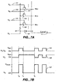
- Figure 7a is similar to Figure 6 and shows most of the same elements.
- the various word line voltages V E are supplied along line 107. This is received by representative word lines WL A , WL B , and WL C respectively through transistors 101, 103, and 105, which are in turn controlled by respective voltages V A , V B , and V C along lines 111, 113, and 115.
- the word lines in Figures 6 and 7a have been labeled WL A , WL B , and WL C .
- word lines can correspond to the word lines of the same block in Figure 2 , such as WL0_i, WL1_i and WL2_i, where only WL2_i has been selected for erase, or may be from different blocks where the block containing WL C has been selected for erase, both those containing WL A and WL B have not.
- Figure 7a also shows the well structure 11 connected to line 107 through diode 121 to receive the voltage V E from line 107. This particular arrangement is somewhat specific to a particular embodiment of the present invention where the level V E corresponds to a voltage that is supplied concurrently to both the well and some of the word lines.
- Figure 7a schematically represents some of the elements from row control circuits 3 ( Figure 1 ) and the c-p-well control 5 that can supply the voltages represented in Figure 7b to the appropriate elements.
- Figure 7b is a set of waveforms for the various voltages applied to Figure 7a in an exemplary embodiment of the preset invention.
- word line WL C corresponds to a selected word line and word lines WL A and WL B correspond to non-selected word lines.
- Waveform 131 is the voltage level controlling the connection of the non-selected word lines to line 107
- waveform 135 is the voltage level controlling the connection of any selected word lines
- 137 is the level on line 107 itself.
- a first phase from t 0 to t 1 in Figure 7b , transistors 101, 103, and 105 are all turned on by supplying Vpp to lines 111, 113, and 115, and the erase voltage V erase is concurrently supplied at V E .
- the result of this erase initialization phase is to set the well and the word lines running across it, both selected and non-selected, to V erase .
- the duration of this phase, (t 1 - t 0 ) can either be hardwired into the system or, preferably, adjustable, either at test time or dynamically in response to operating conditions or device characteristics. For example, a parameter based implementation could be used with the parameter set when the device is subjected to its initial tests.
- the erase phase (or initial erase phase) takes place between times t 1 and t 2 , where the duration here can be determined similarly to that for the initialization phase. Additionally, the corresponding parameter can be dynamically altered based on failure of erase verify or other erase related errors.
- V A and V B are taken low, shutting off transistors 101 and 103 and trapping the erase voltage on non-selected word lines WL A and WL B .
- the erase voltage is also held on the well, in this exemplary embodiment by the diode 121 and more generally by the c-p-well control circuit 5.
- bit lines (BL), select lines (SG) and c-source can be put in a floating state, where they are raised to almost V erase due to a capacitive coupling with the c-p-well and the non-selected word lines.
- bit lines (BL), select lines (SG) and c-source can be put in a floating state, where they are raised to almost V erase due to a capacitive coupling with the c-p-well and the non-selected word lines.
- any of these could also be supplied directly with V erase in a manner similar to that described for the non-selected word lines.
- the erase voltage on the well, the non-selected word lines, or both can be refreshed.
- Figure 7b shows this as occurring after time t 2 .
- the voltage V E is again taken to V erase and, to prevent selected word lines from charging back up, V C is set low to turn off transistor 105.
- V A and V B are taken high, allowing V erase back onto WL A and WL B through respective transistors 101 and 103.
- the c-p-well 11 is also concurrently recharged through diode 121.
- V A , V B , and V E are all taken low and V C is taken high and the erasing of the selected storage elements continues. This refreshing process can be repeated one or more times as needed.
- Figure 7b shows the well 11 and non-selected word lines WL A and WL B both being included in the refresh process, it may not be necessary to do both in some devices.
- V A and V B could be kept low and only the well would be refreshed or, alternatively, the non-selected word lines could be refreshed, but not the well.
- This last variation would require replacing the diode 121 with a transistor or other switch in c-p-well control 5.
- the waveforms 131, 135, and 137 show the duration of the refresh intervals (when 137 is high after t 2 ) to be roughly the same the duration as the subsequent erase intervals (when 137 is low after t 2 ) and the initialization phase (t 1 - t 0 ).
- the refresh intervals will be shorter than the initialization phase, since the voltage level is just being "topped off", and shorter than the subsequently erase phases, which may be closer to the initial erase phase (t 2 -t 1 ) in duration.
- the magnitude of these various durations can be set in hardware, software, or firmware and preferable use a parameter based implementation that can be set at test time or varied dynamically in response to operation conditions or device characteristics. Additionally, the corresponding parameters can be dynamically altered based on failure of erase verify or other erase related errors.
- representative word lines WL A , WL B , and WL C can correspond to the word lines of the same block in Figure 2 or may be from different blocks.
- the use of the techniques described with respect to Figures 7a and 7b can be advantageously used for individual word lines within a single block, such as WL0_i, WL1_i and WL2_i in Figure 2 , where only WL2_i has been selected for erase Figure 2 , it will more commonly be used where WL A , WL B , and WL C correspond to word lines from different blocks.
- a block corresponds to the memories unit of erase.
- many (up to several hundred) blocks may be formed upon a single well and each block will have a number of word lines.
- the unit of erase, or block will differ from the units of writing, or page, and reading, with a block typically including a number of pages (which may, in turn, include one or more sectors, the traditional unit of data transfer).
- the erase process will typically not consist of the erase of a single pages, but of all of the pages within a (physical) block.
- each of the word lines WL A , WL B , and WL C would represent the collective set of word lines in a particular block.
- the input lines for the control gates can be applied to all blocks in the memory, with a block select signal determining which word lines in which blocks actually receive the signals.
- the row control circuits 3 decodes the input lines on the memory device 22 and applies these to all of the blocks of memory array 1. For example, in a read process, only one of these input lines is held at the read voltage, will the non-selected ones are turned fully on; similarly, when programming, only one of the input lines is held at the program voltage, with the rest at a pass voltage. To the restrict the read or write operation to a particular block, only that one block of the, here, 1024 blocks is selected, thereby allowing the input voltages to actually pass to the word lines.
- a main aspect of the present invention is to find an alternative to floating the word lines of all blocks not selected for erase, with the resulting residual potential left across the memory unit, without increasing the size of the memory device, or die, itself.
- the present invention allows the prior art memory structure, as described in the references mentioned to be largely maintained without requiring completely new circuits in the "pitch" portions of the word line layout, by just change their control signals which are generated at one place on the memory device.
- this can be implemented by first raising CG1-CG16 all to Vpp, VRDEC to Vpp, pump Transfer G1 above Vpp at the same time as the p-well of the memory array is taken to Vpp.
- the present invention has a number of advantages over the prior, some of which have already been discussed above. These include less potential erase-induced disturb in non-selected storage elements and a tighter erase distribution in the selected elements. These features are increasingly important as the scale of multi-state non-volatile memory devices continues to decrease, since this scaling typically results in products in which erase inhibit voltage depends strongly on close tracking of coupling ratios. Another aspect of the present invention is that this can be accomplished without increasing the pitch area of the circuit or adding new wires in the memory array. As described above, the various aspects of the present invention can be implemented by introducing minimal additional peripheral area.
- the present invention is applicable not just to the NAND type of flash memory of the exemplary embodiment, but other cases where the storage elements are formed upon a well structure and a process requires a high potential difference to be placed across selected elements.
- other EEPROM or charge storing cells could benefit, e.g. a NOR type flash memory with well erase.
- the storage element is not a floating gate transistor, for example the dielectric storage element of the kind described in the U.S. patent application entitled "Multi-State Non-Volatile Integrated Circuit Memory Systems That Employ Dielectric Storage Elements", by Eliyahou Harari, George Samachisa, Jack H. Yuan, and Daniel C. Guterman, filed October 25, 2002.
Abstract
Description
- This invention relates generally to a non-volatile memory and its operation, and, more specifically, to techniques for insuring controlled erase conditions.
- The principles of the present invention have application to various types of non-volatile memories, those currently existing and those contemplated to use new technology being developed. Implementations of the present invention, however, are described with respect to a flash electrically-erasable and programmable read-only memory (EEPROM), wherein the storage elements are floating gates.
- During the operation of a non-volatile memory, the reading, writing, and erase of data in one storage unit will often disturb the data stored in other storage units of the memory. One source of these disturbs is the field effect coupling between adjacent floating gates as described in
U.S. patent no. 5,867,429 of Jian Chen and Yupin Fong . Additional techniques for reducing such disturbs are described inU.S. patent number 6,522,580 . - This effect and other sources of read and write disturbs are present in various types of flash EEPROM cell arrays. A NOR array of one design has its memory cells connected between adjacent bit (column) lines and control gates connected to word (row) lines. The individual cells contain either one floating gate transistor, with or without a select transistor formed in series with it, or two floating gate transistors separated by a single select transistor. Examples of such arrays and their use in storage systems are given in the following U.S. patents of SanDisk Corporation: Patent Nos.
5,095,344 ,5,172,338 ,5,602,987 ,5,663,901 ,5,430,859 ,5,657,332 ,5,712,180 ,5,890,192 ,6,151,248 ,6,426,893 , and6,512,263 . - A NAND array of one design has a number of memory cells, such as 8, 16 or even 32, connected in series string between a bit line and a reference potential through select transistors at either end. Word lines are connected with control gates of cells in different series strings. Relevant examples of such arrays and their operation are given in
U.S. patent number 6,522,580 . Other examples are given in U.S. patent applications entitled "Highly Compact Non-Volatile Memory and Method Thereof", by Raul-Adrian Cernea, and "Non-Volatile Memory and Method with Reduced Source Line Bias Errors", by Raul-Adrian Cernea and Yan Li, both filed September 24, 2002, and inU.S. patents number 5,546,341 ,5,473,563 and6,373,746 . - It is still most common in current commercial products for each floating gate to store a single bit of data by operating in a binary mode, where only two ranges of threshold levels of the floating gate transistors are defined as storage levels. The threshold levels of a floating gate transistor correspond to ranges of charge levels stored on their floating gates. In addition to shrinking the size of the memory arrays, the trend is to further increase the density of data storage of such memory arrays by storing more than one bit of data in each floating gate transistor. This is accomplished by defining more than two threshold levels as storage states for each floating gate transistor, four such states (2 bits of data per floating gate) now being included in commercial products. More storage states, such as 16 states per storage element, are contemplated. Each floating gate transistor has a certain total range (window) of threshold voltages in which it may practically be operated, and that range is divided into the number of states defined for it plus margins between the states to allow them to be clearly differentiated from one another. In a multi-state nonvolatile memory, the threshold voltage ranges are often increased in comparison with single-bit memories in order to accommodate the all of the multi-states and their margins. Correspondingly, the voltages applied to the control gates during read and programming are correspondingly increased, resulting in more erase, program, and read disturbs. Additionally, as devices move to lower power designs, the available window in which to fit these multi-states is also shrinking further aggravating the problems.
- A common operation of these types of non-volatile memories is to erase blocks of memory cells prior to reprogramming them. The cells within the block are then individually programmed out of erase into states represented by the incoming data being stored. Programming typically includes alternate application to a large number of memory cells in parallel of programming voltage pulses and a reading of their individual states to determine whether the individual cells have reached their intended levels. Programming is stopped for any cell that is verified to have reached its intended threshold level while programming of the other cells being programmed in parallel continues until all of those cells are programmed. When the number of storage states per storage element is increased, the time to perform the programming will usually be increased since the smaller voltage ranges for the individual states requires a greater precision of programming. This can have a significant adverse impact on the performance of the memory systems.
- The narrower ranges of the defined floating gate storage levels that result from multi-state operation increases the level of sensitivity of a first group of storage elements to operations performed on a second group of adjacent storage elements. In an erase operation, the storage elements are typically subjected to a large voltage differential in order to remove charge from the floating gate. As non-selected storage elements are often also subjected to high voltage values, through shared word lines, bit lines, well structures, capacitive couplings, or other mechanisms, this can lead to disturbs on the non-selected storage elements. For example, in a NAND structure such as that described in
U.S. patent number 6,522,580 a high voltage differential is created across selected storage elements by placing their erase gates at ground and raising the well structure of the array to a high erase voltage. Non-selected storage elements may also be upon this well structure. Although it is common in the prior art to allow unselected erase gates to be charged by capacitive couplings from the well (as is described, for example, inU.S. patent number 5,546,341 ), there will still be a potential placed across the storage element that can lead to disturbs. If the number of erroneous bits is maintained within the capability of an error correction code (ECC), the errors are corrected but if the number of errors is typically larger than that, some other structural and/or operating technique(s) needs to be employed. It is desired to provide techniques to reduce erase disturbs in non-volatile memories to further increase their performance. - [0008A]
US 2002/167844 discloses a memory in which a positive erase voltage is applied to a well structure while a negative voltage is applied to the control gates of the memory cells to be erased. The control gate of the memory cells that are not to be erased are biased to a smaller positive voltage or remain unbiased. The independent claims are characterised over this document. - [0009A] According to an aspect of the present invention there is provided a method of erasing a selected one of a plurality of storage elements formed upon a well structure in a non-volatile memory. The method comprises selecting one or more but less than all of said storage elements for erase, holding the well structure at an erase voltage, concurrently with holding the well structure at the erase voltage raising the voltage level on a control gate of the non-selected storage elements above that which results from the capacitive coupling to the well structure and concurrently with holding the well structure at the erase voltage, lowering the voltage level on a control gate of the selected storage elements to below the erase voltage.
- [0009B] According to another aspect of the present invention there is provided a non-volatile memory comprising a plurality of storage units formed upon a substrate, a well structure in the substrate upon which the storage units are formed and means for maintaining, during an erase process of selected storage elements, the well structure and non-selected ones of the storage elements at an erase voltage while allowing the control gates of the selected storage elements to discharge.
- [0009C] In a preferred embodiment the selected word-lines are discharged to ground while the non-selected word-lines and the well are maintained at the high voltage. As an option, during the erase cycle the inhibited storage elements may be periodically refreshed to the well potential (high voltage) and/or the selected word-lines can be floated and/or periodically refreshed to ground.
- In an exemplary embodiment, a flash memory with a NAND architecture is used. A large number of blocks, the unit of erase, are formed upon a single well structure. Each block contains a number of words lines to which the control gates of the memory units are connected. The control gates of the memory units over the well are charged to the erase voltage at the same time as the well itself. The charge is then trapped on the word lines of the non-selected blocks during the erase process, thereby setting the same voltage level on both the control gates and the well so that no potential is placed across the charge storing element. In a selected block, the word lines are discharged, setting up a voltage difference across the floating gate and leading to its erase.
- This can be accomplished without increasing any pitch area circuit or adding new wires in the memory array, and at minimal additional peripheral area. By appropriate changes to the decoding on the memory device, the structure within the array portion of the memory device can be maintained while allowing the non-selected word lines to be held at a voltage above that which would be obtained through capacitative coupling to the substrate alone. Advantages include less potential erase disturb in the non-selected storage elements and a tighter erase distribution for the selected elements.
- Additional aspects, features and advantages of the present invention are included in the following description of exemplary embodiments, which description should be taken in conjunction with the accompanying drawings.
-
Figure 1 is a block diagram of a non-volatile memory system in which the various aspects of the present invention are described to be implemented; -
Figure 2 illustrates an existing circuit and organization of the memory array ofFigure 1 when a NAND type; -
Figure 3 shows a cross-sectional view, along a column, of a NAND type of memory array formed on a semiconductor substrate; -
Figure 4 is a cross-sectional view of the memory array ofFigure 3 , taken at section 4-4 thereof; -
Figure 5 is a cross-sectional view of the memory array ofFigure 3 , taken at section 5-5 thereof; -
Figure 6 schematically illustrates a prior art erase arrangement; and -
Figures 7a and 7b show aspects of an exemplary embodiment of the present invention. - With reference to
Figures 1-7 , a specific non-volatile memory system is described in which the various aspects of the present invention are implemented, in order to provide specific examples. To reduce the amount of disturb in erase processes, the present invention maintains the control gates of non-selected storage elements at the same voltage level as their underlying well structure. In a exemplary embodiment, the storage elements are formed over a well structure. During an erase process, both the selected and non-selected storage elements over the well are raised to an erase voltage concurrently with establishing this voltage level in the well. This voltage is then held on the well and the non-selected storage elements, thereby reducing the chance of any erase related disturbs, while the selected storage elements are allowed to discharge, producing the needed erase conditions. Further, this can be accomplished without increasing any pitch area of circuit or adding new wires in the memory array, resulting in minimal additional peripheral area being added to the circuit. - For specificity, the present invention is described for an EEPROM flash memory of the NAND type, although generalizations will be discussed further below. In particular, the present exposition will use the sort of system described in
U.S. patent number 6,522,580 and the other applications related to NAND systems that are referred to above. When specific voltages are needed in the following, the erase voltage Verase is taken to be in the 15-20 volt range, the low logic level is taken as ground, and the high logic level Vdd taken in the 1.5-3 volt range, although other values can be used, depending on design. -
Figure 1 is a block diagram of a flash memory system.Memory cell array 1 including a plurality of storage units M arranged in a matrix is controlled by acolumn control circuit 2, arow control circuit 3, a c-source control circuit 4 and a c-p-well control circuit 5. Thecolumn control circuit 2 is connected to bit lines (BL) of thememory cell array 1 for reading data stored in the memory cells (M), for determining a state of the memory cells (M) during a program operation, and for controlling potential levels of the bit lines (BL) to promote the programming or to inhibit the programming. Therow control circuit 3 is connected to word lines (WL) to select one of the word lines (WL), to apply read voltages, to apply a program voltages combined with the bit line potential levels controlled by thecolumn control circuit 2, and to apply an erase voltage coupled with a voltage of p-type regions (labeled as "c-p-well" 11 inFigure 3 ) on which the memory cells (M) are formed. The c-source control circuit 4 controls the common source lines (labeled as "c-source" inFigure 2 ) connected to the memory cells (M). The c-p-well control circuit 5 controls the voltage of the c-p-well. - The data stored in the memory cells (M) are read out by the
column control circuit 2 and are output to external I/O lines via an I/O line and a data input/output buffer 6. Program data to be stored in the memory cells are input to the data input/output buffer 6 via the external I/O lines, and transferred to thecolumn control circuit 2. The external I/O lines are connected to a controller 20. Command data for controlling the flash memory device are input to a command interface connected to external control lines, which are connected with the controller 20. The command data informs the flash memory of what operation is requested. The input command is transferred to astate machine 8 that controls thecolumn control circuit 2, therow control circuit 3, the c-source control circuit 4, the c-p-well control circuit 5 and the data input/output buffer 6. Thestate machine 8 can output a status data of the flash memory such as READY/BUSY or PASS/FAIL. - The controller 20 is connected or connectable with a host system such as a personal computer, a digital camera, or a personal digital assistant. The host initiates commands, such as to store or read data to or from the
memory array 1, and provides or receives such data, respectively. The controller converts such commands into command signals that can be interpreted and executed by the command circuits 7. The controller also typically contains buffer memory for the user data being written to or read from the memory array. A typical memory system includes one integratedcircuit chip 21 that includes the controller 20, and one or moreintegrated circuit chips 22 that each contain a memory array and associated control, input/output and state machine circuits. The trend, of course, is to integrate the memory array and controller circuits of a system together on one or more integrated circuit chips. The memory system may be embedded as part of the host system, or may be included in a memory card that is removably insertable into a mating socket of host systems. Such a card may include the entire memory system, or the controller and memory array, with associated peripheral circuits, may be provided in separate cards. - With reference to
Figure 2 , an example structure of thememory cell array 1 is described. A flash EEPROM of a NAND type is described as an example. The memory cells (M) are partitioned into a number of blocks, 1,024 in a specific example. The data stored in each block are simultaneously erased. The block is thus the minimum unit of a number of cells that are simultaneously erasable. In each block, there are N columns, N=8,512 in this example, that are divided into left columns and right columns, as described in furtherU.S. patent number 6,522,580 . The bit lines are also divided into left bit lines (BLL) and right bit lines (BLR). Four memory cells connected to the word lines (WL0 to WL3) at each gate electrode are connected in series to form a NAND cell unit. One terminal of the NAND cell unit is connected to corresponding bit line (BL) via a first select transistor (S) which gate electrode is coupled to a first (Drain) select gate line (SGD), and another terminal is connected to the c-source via a second (Source) select transistor (S) which gate electrode is coupled to a second select gate line (SGS). Although four floating gate transistors are shown to be included in each cell unit, for simplicity, other numbers of transistors, such as 8, 16, or even 32, are used.Figure 2 also includes a connection, C-p-well, for supplying the well voltage. - In each block, in this example, 8,512 columns are divided into even columns and odd columns. The bit lines are also divided into even bit lines (BLe) and odd bit lines (BLo). Four memory cells connected to the word lines (WL0 to WL3) at each gate electrode are connected in series to form a NAND cell unit. One terminal of the NAND cell unit is connected to corresponding bit line (BL) via a first select transistor (S) which gate electrode is coupled to a first select gate line (SGD), and another terminal is connected to the c-source via a second select transistor (S) which gate electrode is coupled to a second select gate line (SGS). Although, for simplicity, four floating gate transistors are shown to be included in each cell unit, a higher number of transistors, such as 8, 16 or even 32, are used.
- In an alternate set of embodiments, as described in
U.S. patent application andserial number 10/086495, filed February 27, 2002granted as US 6,771,536 the array can be divided into left and right portions instead of the odd-even arrangement. The left and right sides may additionally have independent well structures with the right and left sides of the array each formed over such separate well structures, allowing the voltage levels to be set independently by the c-p-well control circuit 5 ofFigure 1 . In a further variation, this could also allow erasure of a sub-block of less than all of the partitions of a block. Further variations that are compatible with the present invention are also described inapplication number 10/086495. - In the exemplary embodiments, the page size is 512 bytes, which is smaller than the cell numbers on the same word line. This page size is based on user preference and convention. Allowing the word line size to correspond to more than one page's worth of cells saves the X-decoder (row control circuit 3) space since different pages worth of data can share the decoders. During a user data read and programming operation, N=4,256 cells (M) are simultaneously selected in this example. The cells (M) selected have the same word line (WL), for example WL2, and the same kind of bit line (BL). Therefore, 532 bytes of data can be read or programmed simultaneously. This 532B data simultaneously read or programmed forms a "page" logically. Therefore, one block can store at least eight pages. When each memory cell (M) stores two bits of data, namely a multi-level cell, one block stores 16 pages in the case of two bit per cell storage. In this embodiment, the storage element of each of the memory cells, in this case the floating gate of each of the memory cells, stores two bits of user data.
-
Figure 3 shows a cross sectional view of a NAND cell unit of the type shown schematically inFigure 2 , in the direction of the bit line (BL). At a surface of a p-type semiconductor substrate 9, a p-type region c-p-well 11 is formed, each of the left and right c-p-wells being enclosed by an n-type region 10 to electrically isolate the c-p-wells from the p-type substrate. The n-type region 10 is connected to a c-p-well line made of a first metal M0 via a first contact hole (CB) and an n-type diffusion layer 12. The p-type region c-p-well 11 is also connected to the c-p-well line via the first contact hole (CB) and a p-type diffusion layer 13. The c-p-well line is connected to the c-p-well control circuit 5 (Figure 1 ). - The exemplary embodiment uses Flash EEPROM storage units, where each memory cell has a floating gate (FG) that stores an amount of electric charge corresponding to the data being stored in the cell, the word line (WL) forming the gate electrode, and drain and source electrodes made of the p-
type diffusion layer 12. The floating gate (FG) is formed on the surface of the c-p-well via a tunnel oxide film (14). The word line (WL) is stacked on the floating gate (FG) via an insulator film (15). The source electrode is connected to the common source line (c-source) made of the first metal (M0) via the second select transistor (S) and the first contact hole (CB). The common source line is connected to the c-source control circuit (4). The drain electrode is connected to the bit line (BL) made of a second metal (M1) via the first select transistor (S), the first contact hole (CB), an intermediate wiring of the first metal (M0) and a second contact hole (V1). The bit line is connected to the column control circuit (2). -
Figures 4 and 5 show cross sectional views of a memory cell (section 4-4 ofFigure 3 ) and a select transistor (section 5-5 ofFigure 3 ), respectively, in the direction of the word line (WL2). Each column is isolated from the neighbor columns by a trench formed in the substrate and filled with isolation material, known as a shallow trench isolation (STI). The floating gates (FG) are isolated from each other by the STI andinsulator film 15 and word line (WL). Since the gate electrode (SG) of the select transistor (S) is formed in the same formation process steps as the floating gate (FG) and word line (WL), it shows a stacked gate structure. These two select gate lines (SG) are shunted at the end of lines. -
U.S. patent number 6,522,580 referred to above describes the varoius voltages applied to operate thememory cell array 1, in a specific example, each memory cell's floating gate storing two bits, having one of the states "11", "10", "01", "00". This is reviewed briefly here for the case where the word line "WL2" and the bit lines of "BLe" are selected for erase, reading or programming. By raising the c-p-well to an erase voltage of Verase=15-20V and grounding the word lines (WL) of a selected block, the data of the selected block is erased. Since all of the word lines (WL) of the unselected blocks, bit lines (BL), select lines (SG) and c-source are put in a floating state, these are also raised to almost Verase due to a capacitive coupling with the c-p-well. Therefore, a strong electric field is applied to only the tunnel oxide films 14 (Figures 4 and 5 ) of the selected memory cells (M), and the data of the selected memory cells are erased as a tunnel current flows across thetunnel oxide film 14. The erased cell is, in this example, one of the four possible programmed states, namely "11". - The high voltage values used in the erase and programming values can be generated from the lower supply values using a charge pump (not shown in
Figure 1 ). These higher voltage values can either be produced on thememory chip 22 itself, or supplied form another chip in the memory system. The use and location of the high voltage source is discussed more fully inU.S. patent number 6,282,130 and additional references cited therein. -
Figure 6 schematically illustrates such a prior art arrangement. Three representative word lines, WLA, WLB, and WLC are connected to aline 107 that supplies the various voltage levels throughtransistors transistors line 107 would be part of therow control circuit 3 ofFigure 1 . The c-p-well control circuit 5 ofFigure 1 provides the voltage for the well structure c-p-well 11. The word lines then continue on over thewell structure 11 to any of the various word lines of the different blocks ofmemory 1 shown inFigure 2 . In a erase process, with word line WLC corresponding to a selected word line and WLA and VLB both non-selected, the voltage in the c-p-well is raised to the erase voltage of, say, 17 volts andline 107 is set to ground. The gate oftransistor 105 is set to the high level of Vdd, taking word line WLC to ground, while both oftransistors U.S. patent number 5,546,341 referred to above) and the selected erase gates are forced to ground. Other aspects of the erase process are described inU.S. patent application number 09/956,201, filed September 17, 2001 US 6,741,502 . In particular,U.S. patent application number 09/956,201 describes a process where the non-selected word-lines can be floated, a process which can also be incorporated into alternate embodiments of the various aspects of the present invention. - In order to store electrons in the floating gate (FG) during a programming operation, the selected word line WL2 is connected to a program pulse Vpgm and the selected bit lines BLe are grounded. On the other hand, in order to inhibit the program on the memory cells (M) in which programming is not to take place, the corresponding bit lines BLe are connected to Vdd of a power supply, for example 3V, as well as the unselected bit lines BLo. The unselected word lines WL0, WL1 and WL3 are connected to 10V, the first select gate (SGD) is connected to Vdd, and the second select gate (SGS) is grounded. As a result, a channel potential of the memory cell (M) that is being programmed is set at 0V. The channel potential in the program inhibition is raised to around 6V as a result of the channel potential being pulled up by the capacitive coupling with the word lines (WL). As explained above, a strong electric field is applied to only the
tunnel oxide films 14 of the memory cells (M) during programming, and the tunnel current flows across thetunnel oxide film 14 in the reverse direction compared to the erase, and then the logical state is changed from "11" to one of the other states "10", "01", or "00". - In order to store electrons in the floating gate (FG) during a programming operation, the selected word line WL2 is connected to a program pulse Vpgm and the selected bit lines BLe are grounded. On the other hand, in order to inhibit the program on the memory cells (M) in which programming is not to take place, the corresponding bit lines BLe are connected to Vdd of a power supply, for example 3V, as well as the unselected bit lines BLo. The unselected word lines WL0, WL1 and WL3 are connected to 10V, the first select gate (SGD) is connected to Vdd, and the second select gate (SGS) is grounded. As a result, a channel potential of the memory cell (M) that is being programmed is set at 0V. The channel potential in the program inhibition is raised to around 6V because of the channel potential being pulled up by the capacitive coupling with the word lines (WL). As explained above, a strong electric field is applied to only the
tunnel oxide films 14 of the memory cells (M) during programming, and the tunnel current flows across thetunnel oxide film 14 in the reverse direction compared to the erase, and then the logical state is changed from "11" to one of the other states "10", "01", or "00". - In the read and verify operations, the select gates (SGD and SGS) and the unselected word lines (WL0, WL1 and WL3) are raised to a read pass voltage of 4.5V to make these as pass gates. The selected word line (WL2) is connected to a voltage level specified for each read and verify operation in order to determine whether a threshold voltage of the concerned memory cell has reached such level. For example, in a
READ 10 operation, the selected word line WL2 is grounded, so that it is detected whether the threshold voltage is higher than 0V. In this read case, it can be said that a read level is 0V. In a VERIFY 01 operation, the selected word line WL2 is connected to 2.4V, so that it is verified that whether the threshold voltage has reached 2.4V. In this verify case, it can be said that a verify level is 2.4V. Again, for all of the described processes, the recited voltage levels are only exemplary values. - The selected bit lines (BLe) are pre-charged to a high level, for example 0.7V. If the threshold voltage is higher than the read or verify level, the potential level of the concerned bit line (BLe) maintains the high level, because of the non-conductive memory cell (M). On the other hand, If the threshold voltage is lower than the read or verify level, the potential level of the concerned bit line (BLe) decreases to a low level, for example less than 0.5V, because of the conductive memory cell (M). Further details of the read and verify operations are explained below.
- In the erase operation described above, the selected word lines are held at ground to provide the desired potential difference between the cells control gate and the erase voltage in the well structure. The non-selected cells depend upon capacitive coupling between their control gates and the well to raise the control gates to a high enough value so that these cells are not erased. Although the capacitive coupling will raise the non-selected word lines, such as WLA and WLB in
Figure 6 , to near well level, it will not be raised to the full value, causing a potential difference to be set up across the connected cells. This can result in some of the stored charge being lost from the floating gates and eventually resulting in a possible disturb, particularly in low voltage, multi-state devices. In a principle aspect, the present invention raises the voltage level on the non-selected word lines above what would result from the capacitive coupling alone, thereby reducing or eliminating the potential difference between non-selected control gate -
Figure 7a is similar toFigure 6 and shows most of the same elements. The various word line voltages VE are supplied alongline 107. This is received by representative word lines WLA, WLB, and WLC respectively throughtransistors lines Figures 6 and7a have been labeled WLA, WLB, and WLC. These word lines can correspond to the word lines of the same block inFigure 2 , such as WL0_i, WL1_i and WL2_i, where only WL2_i has been selected for erase, or may be from different blocks where the block containing WLC has been selected for erase, both those containing WLA and WLB have not.Figure 7a also shows thewell structure 11 connected toline 107 throughdiode 121 to receive the voltage VE fromline 107. This particular arrangement is somewhat specific to a particular embodiment of the present invention where the level VE corresponds to a voltage that is supplied concurrently to both the well and some of the word lines. More generally, this particular connection is used only when this condition is met and, even in those circumstance, the well voltage can be supplied by the c-p-well control 5 (Figure 1 ) as described in the various incorporated references. In any case, for the exemplary embodiment of the present invention,Figure 7a schematically represents some of the elements from row control circuits 3 (Figure 1 ) and the c-p-well control 5 that can supply the voltages represented inFigure 7b to the appropriate elements. -
Figure 7b is a set of waveforms for the various voltages applied toFigure 7a in an exemplary embodiment of the preset invention. In this example, word line WLC corresponds to a selected word line and word lines WLA and WLB correspond to non-selected word lines.Waveform 131 is the voltage level controlling the connection of the non-selected word lines toline 107,waveform 135 is the voltage level controlling the connection of any selected word lines, and 137 is the level online 107 itself. - In a first phase, from t0 to t1 in
Figure 7b ,transistors lines - The erase phase (or initial erase phase) takes place between times t1 and t2, where the duration here can be determined similarly to that for the initialization phase. Additionally, the corresponding parameter can be dynamically altered based on failure of erase verify or other erase related errors. In this phase, VA and VB are taken low, shutting off
transistors diode 121 and more generally by the c-p-well control circuit 5. During the erase process, the other terminals of the memory can be treated as discussed above with respect toFigure 6 ; namely, the bit lines (BL), select lines (SG) and c-source can be put in a floating state, where they are raised to almost Verase due to a capacitive coupling with the c-p-well and the non-selected word lines. In a various of the present invention, any of these could also be supplied directly with Verase in a manner similar to that described for the non-selected word lines. - In another aspect of the present invention, the erase voltage on the well, the non-selected word lines, or both can be refreshed.
Figure 7b shows this as occurring after time t2. The voltage VE is again taken to Verase and, to prevent selected word lines from charging back up, VC is set low to turn offtransistor 105. To recharge the non-selected word lines, VA and VB are taken high, allowing Verase back onto WLA and WLB throughrespective transistors diode 121. Subsequently, VA, VB, and VE are all taken low and VC is taken high and the erasing of the selected storage elements continues. This refreshing process can be repeated one or more times as needed. - Although
Figure 7b shows the well 11 and non-selected word lines WLA and WLB both being included in the refresh process, it may not be necessary to do both in some devices. For example, VA and VB could be kept low and only the well would be refreshed or, alternatively, the non-selected word lines could be refreshed, but not the well. (This last variation would require replacing thediode 121 with a transistor or other switch in c-p-well control 5.) Also, for exemplary purposes, thewaveforms - As noted above, representative word lines WLA, WLB, and WLC can correspond to the word lines of the same block in
Figure 2 or may be from different blocks. Although the use of the techniques described with respect toFigures 7a and 7b can be advantageously used for individual word lines within a single block, such as WL0_i, WL1_i and WL2_i inFigure 2 , where only WL2_i has been selected for eraseFigure 2 , it will more commonly be used where WLA, WLB, and WLC correspond to word lines from different blocks. - Returning to the exemplary embodiment described above with respect to
Figures 1-5 and developed further inU.S. patent numbers 6,522,580 and6,373,746 , a block corresponds to the memories unit of erase. Typically, many (up to several hundred) blocks may be formed upon a single well and each block will have a number of word lines. Generally, the unit of erase, or block, will differ from the units of writing, or page, and reading, with a block typically including a number of pages (which may, in turn, include one or more sectors, the traditional unit of data transfer). Thus, the erase process will typically not consist of the erase of a single pages, but of all of the pages within a (physical) block. Within this structure, each of the word lines WLA, WLB, and WLC would represent the collective set of word lines in a particular block. As described in the cited references, for a exemplary embodiment the input lines for the control gates can be applied to all blocks in the memory, with a block select signal determining which word lines in which blocks actually receive the signals. - For example, with reference to
Figures 1-3 , the row control circuits 3 (along withstate machine 8 and command circuits 7) decodes the input lines on thememory device 22 and applies these to all of the blocks ofmemory array 1. For example, in a read process, only one of these input lines is held at the read voltage, will the non-selected ones are turned fully on; similarly, when programming, only one of the input lines is held at the program voltage, with the rest at a pass voltage. To the restrict the read or write operation to a particular block, only that one block of the, here, 1024 blocks is selected, thereby allowing the input voltages to actually pass to the word lines. - More detail on suitable circuitry which can be adapted to the present invention is given in
U.S. patent number 6,373,746 referred to above for the case of 16 word lines per block and where the signals CG1-CG16 are the input voltages. Figure 17 of patent number 6,373,746 describes a block decoding circuit in which, for a given block, the signal Transfer G1 corresponds to VA, VB, VC ofFigure 7 here. In the prior, as shown here inFigure 6 , when a particular block i is selected for erase, this signal is high for the selected block and low for the non-selected blocks. The word lines WL1_i - WL16_i are all grounded and the memory devices in that block are erased. As the other blocks are left floating and, due to the capacitive coupling, are raised towards the substrate voltage, relatively little voltage difference is placed across the non-selected memory cells. (The passing or not passing of CG1-CG16 to the word lines occurs via the polarity of RDECAD as derived from Figure 16 of patent number 6,373,746. For the selected block this signal is high; for all the unselected blocks this signal is low. Then VRDEC is put to VPP and Transfer G1 is pumped higher than VPP (either on the memory device itself or imported from another device) and these values are applied as shown here inFigure 6 , for the prior art, and inFigures 7a and 7b for the present invention.) - As described above, a main aspect of the present invention is to find an alternative to floating the word lines of all blocks not selected for erase, with the resulting residual potential left across the memory unit, without increasing the size of the memory device, or die, itself. The present invention allows the prior art memory structure, as described in the references mentioned to be largely maintained without requiring completely new circuits in the "pitch" portions of the word line layout, by just change their control signals which are generated at one place on the memory device. Again referring to Figures 16 and 17 of
U.S. patent number 6,373,746 , this can be implemented by first raising CG1-CG16 all to Vpp, VRDEC to Vpp, pump Transfer G1 above Vpp at the same time as the p-well of the memory array is taken to Vpp. The decoding (inputs to Figure 16) then needs to be altered (with respect to patent 6,373,746) to de-select any blocks, which has the effect of putting Vpp on all word lines. Transfer G1 is deselected so that all word lines are floating (but pre-charged to Vpp), then the proper decoding signals are applied while moving CG1-CG16 all to ground. This has the effect of placing ground on all 16 word lines of the selected block only, and causes that block to be erased. As shown here inFigure 7b , this cycle can be repeated multiple times if it is desired to refresh the floating word lines held at Vpp. - The present invention has a number of advantages over the prior, some of which have already been discussed above. These include less potential erase-induced disturb in non-selected storage elements and a tighter erase distribution in the selected elements. These features are increasingly important as the scale of multi-state non-volatile memory devices continues to decrease, since this scaling typically results in products in which erase inhibit voltage depends strongly on close tracking of coupling ratios. Another aspect of the present invention is that this can be accomplished without increasing the pitch area of the circuit or adding new wires in the memory array. As described above, the various aspects of the present invention can be implemented by introducing minimal additional peripheral area.
- As noted above, the present invention is applicable not just to the NAND type of flash memory of the exemplary embodiment, but other cases where the storage elements are formed upon a well structure and a process requires a high potential difference to be placed across selected elements. In particular, other EEPROM or charge storing cells could benefit, e.g. a NOR type flash memory with well erase. It can similarly be extended to where the storage element is not a floating gate transistor, for example the dielectric storage element of the kind described in the U.S. patent application entitled "Multi-State Non-Volatile Integrated Circuit Memory Systems That Employ Dielectric Storage Elements", by Eliyahou Harari, George Samachisa, Jack H. Yuan, and Daniel C. Guterman, filed October 25, 2002.
- Although the various aspects of the present invention have been described with respect to specific embodiments, it will be understood that the invention is protected within the full scope of the appended claims.
Claims (25)
- A method of erasing a selected one of a plurality of storage elements formed upon a well structure (11) in a non-volatile memory comprising:selecting one or more but less than all of said storage elements for erase; holding the well structure (11) at an erase voltage;CHARACTERISED BY:concurrently with holding the well structure (11) at the erase voltage, raising the voltage level on a control gate of the non-selected storage elements above that which results from the capacitive coupling to the well structure; andconcurrently with holding the well structure (11) at the erase voltage, lowering the voltage level on a control gate of the selected storage elements to below the erase voltage.
- The method of claim 1, wherein said raising the voltage level on a control gate of the non-selected storage elements above that which results from the capacitive coupling to the well structure (11) comprises:charging the control gate of each of the non-selected storage elements to the erase voltage concurrently with charging the well structure (11) and subsequently maintaining the erase voltage on the non-selected control gates.
- The method of claim 1 or 2, wherein said lowering the voltage level on the control gate of the selected storage elements comprises:allowing the control gate of the selected storage elements to discharge.
- The method of Claim 3 as dependent on Claim 2, wherein said maintaining comprises trapping charge on the well structure (11) and the non-selected control gates while allowing the control gate of the selected storage element to discharge.
- The method of Claim 4, wherein said holding further comprises refreshing the charge level trapped on the well structure (11).
- The method of Claim 5, wherein said maintaining further comprises refreshing the charge level trapped on the non-selected control gates concurrently with refreshing the charge level trapped on the well structure (11).
- The method of Claim 4, wherein said maintaining further comprises refreshing the charge level trapped on the non-selected control gates.
- The method of any preceding claim, wherein said plurality of storage elements are included in an array (1) of such storage elements and wherein the control gates of the array's storage element are connected to word-lines whereby the voltage level of the control gates is set.
- The method of Claim 2, wherein the array is part of a first chip (22), further comprising:generating the said erase voltage on a second chip; andtransferring the erase voltage to the first chip (22) for use in said concurrently charging the well structure (11) and a control gate of each of said storage elements.
- A non-volatile memory comprising:a plurality of storage units formed upon a substrate; anda well structure (11) in the substrate upon which the storage units are formed;CHARACTERISED BY:means for maintaining during an erase process of selected storage elements, the well structure (11) at an erase voltage and raising the voltage level on a control gate of non-selected ones of the storage elements above an erase voltage which results from the capacitive coupling to the well structure while allowing the control gates of the selected storage elements to discharge.
- The non-volatile memory of Claim 10, wherein the means for maintaining comprises control circuitry (3,5) connectable to the substrate (11) and a control gate of each of the plurality storage units and arranged to concurrently set the voltage level of the well structure (11) and said control gates to an erase voltage, and further to allow the control gate of selected ones of the storage elements to discharge the erase voltage while maintaining the erase voltage on the well structure (11) and non-selected ones of the storage elements.
- The non-volatile memory of Claim 11, wherein the storage units are arranged into a plurality of rows, further comprising:a plurality of word lines each connecting the storage elements of a respective row whereby said control circuitry is connectable to the control gate of each of the plurality storage units.
- The non-volatile memory of Claim 12, wherein the storage units form part of an array having a NAND architecture.
- The non-volatile memory of Claim 12 or Claim 13, wherein the control circuit (3) allows the selected control gates to discharge by connecting the respective word line to ground.
- The non-volatile memory of Claim 14, wherein the control circuit (3) maintains the erase voltage on the non-selected storage elements by trapping charge on the respective word lines.
- The non-volatile memory of Claim 14, wherein the control circuit maintains the erase voltage on the well structure (11) by refreshing the charge level trapped on the well structure (11).
- The non-volatile memory of the Claim 16, wherein the control circuit maintains the erase voltage on the non-selected control gates by refreshing the charge level trapped on corresponding word lines concurrently with refreshing the charge level trapped on the well structure (11).
- The non-volatile memory of Claim 14, wherein the control circuit (3) maintains the erase voltage on the non-selected control gates by refreshing the charge level trapped on corresponding word lines.
- The non-volatile memory of Claim 12, wherein the non-volatile memory is physically organised into a plurality of erase units each consisting of a plurality of said word lines, and wherein said control circuitry (3) selects the word lines of a given unit of erase for erase as a group.
- The non-volatile memory of any of Claims 11 to 19, wherein the storage units are multi-state storage units.
- The non-volatile memory of Claim 20, wherein the memory is a flash memory.
- The non-volatile memory of any of Claims 11 to 21, wherein the erase voltage is supplied to the control circuit from external to the memory.
- A system comprising the memory of Claim 12, wherein:the control circuitry is connectable to the word lines;the system further comprising a voltage source connectable to the memory wherein the erase voltage is generated; anda controller connected to the memory for selecting memory cells for erase.
- The system of Claim 23, wherein the voltage source is on the same chip (22) as the memory.
- The system of Claim 23, wherein the voltage source is on a different chip than the memory.
Applications Claiming Priority (2)
| Application Number | Priority Date | Filing Date | Title |
|---|---|---|---|
| US10/671,847 US6958936B2 (en) | 2003-09-25 | 2003-09-25 | Erase inhibit in non-volatile memories |
| PCT/US2004/031082 WO2005031753A1 (en) | 2003-09-25 | 2004-09-21 | Erase inhibit in non-volatile memories |
Publications (2)
| Publication Number | Publication Date |
|---|---|
| EP1665282A1 EP1665282A1 (en) | 2006-06-07 |
| EP1665282B1 true EP1665282B1 (en) | 2008-12-24 |
Family
ID=34376203
Family Applications (1)
| Application Number | Title | Priority Date | Filing Date |
|---|---|---|---|
| EP04788913A Active EP1665282B1 (en) | 2003-09-25 | 2004-09-21 | Erase inhibit in non-volatile memories |
Country Status (9)
| Country | Link |
|---|---|
| US (2) | US6958936B2 (en) |
| EP (1) | EP1665282B1 (en) |
| JP (1) | JP2007507055A (en) |
| KR (1) | KR101062152B1 (en) |
| CN (1) | CN1856840B (en) |
| AT (1) | ATE418785T1 (en) |
| DE (1) | DE602004018663D1 (en) |
| TW (1) | TWI248618B (en) |
| WO (1) | WO2005031753A1 (en) |
Families Citing this family (34)
| Publication number | Priority date | Publication date | Assignee | Title |
|---|---|---|---|---|
| AU2002310388A1 (en) * | 2001-06-06 | 2002-12-16 | Telephonics Corporation | Improved method, system and apparatus for opening doors |
| US6958936B2 (en) * | 2003-09-25 | 2005-10-25 | Sandisk Corporation | Erase inhibit in non-volatile memories |
| KR100528482B1 (en) * | 2003-12-31 | 2005-11-15 | 삼성전자주식회사 | Flash memory system capable of inputting/outputting sector dara at random |
| KR100582422B1 (en) * | 2004-05-15 | 2006-05-22 | 에스티마이크로일렉트로닉스 엔.브이. | Nand flash memory device |
| JP4709523B2 (en) * | 2004-10-14 | 2011-06-22 | 株式会社東芝 | Nonvolatile semiconductor memory device |
| KR100749736B1 (en) * | 2005-06-13 | 2007-08-16 | 삼성전자주식회사 | Flash memory device and erase method thereof |
| US7495954B2 (en) | 2006-10-13 | 2009-02-24 | Sandisk Corporation | Method for partitioned erase and erase verification to compensate for capacitive coupling effects in non-volatile memory |
| KR101062032B1 (en) * | 2006-10-13 | 2011-09-05 | 샌디스크 코포레이션 | Partitioned erase and erase verification in nonvolatile memory |
| US7499317B2 (en) * | 2006-10-13 | 2009-03-03 | Sandisk Corporation | System for partitioned erase and erase verification in a non-volatile memory to compensate for capacitive coupling |
| US7535766B2 (en) * | 2006-10-13 | 2009-05-19 | Sandisk Corporation | Systems for partitioned soft programming in non-volatile memory |
| US7499338B2 (en) * | 2006-10-13 | 2009-03-03 | Sandisk Corporation | Partitioned soft programming in non-volatile memory |
| JP2008117471A (en) * | 2006-11-02 | 2008-05-22 | Toshiba Corp | Nonvolatile semiconductor storage device and nonvolatile memory system |
| US7495958B2 (en) * | 2006-11-06 | 2009-02-24 | Taiwan Semiconductor Manufacturing Company, Ltd. | Program and erase methods and structures for byte-alterable flash memory |
| KR100889780B1 (en) * | 2007-04-24 | 2009-03-20 | 삼성전자주식회사 | Flash memory device capable of improving pass voltage window and program method thereof |
| US7969783B2 (en) | 2007-06-15 | 2011-06-28 | Micron Technology, Inc. | Memory with correlated resistance |
| KR101489885B1 (en) * | 2007-11-21 | 2015-02-06 | 삼성전자주식회사 | Charge Trap Nonvolatile Memory Device With Enhanced Reliability And Method Of Operating The Same |
| KR20090061344A (en) * | 2007-12-11 | 2009-06-16 | 삼성전자주식회사 | Semiconductor memory device having mat structure |
| KR100938094B1 (en) * | 2008-03-14 | 2010-01-21 | 주식회사 하이닉스반도체 | Semiconductor memory device ans method for erase of the same |
| KR101503875B1 (en) | 2008-03-17 | 2015-03-25 | 삼성전자주식회사 | Semiconductor Device Capable Of Suppressing Short Channel Effect And Method Of Fabricating The Same |
| KR101407361B1 (en) * | 2008-04-14 | 2014-06-13 | 삼성전자주식회사 | Non-volatile memory device and program method thereof |
| US7851846B2 (en) * | 2008-12-03 | 2010-12-14 | Silicon Storage Technology, Inc. | Non-volatile memory cell with buried select gate, and method of making same |
| JP2011138579A (en) * | 2009-12-28 | 2011-07-14 | Toshiba Corp | Non-volatile semiconductor memory device |
| US8416624B2 (en) | 2010-05-21 | 2013-04-09 | SanDisk Technologies, Inc. | Erase and programming techniques to reduce the widening of state distributions in non-volatile memories |
| TWI462106B (en) * | 2012-05-07 | 2014-11-21 | Macronix Int Co Ltd | Method and apparatus for reducing erase disturb of memory circuit by using recovery bias |
| US9389999B2 (en) * | 2012-08-17 | 2016-07-12 | Infineon Technologies Ag | System and method for emulating an EEPROM in a non-volatile memory device |
| KR102157863B1 (en) | 2014-09-01 | 2020-09-22 | 삼성전자주식회사 | Nonvolatile memory device |
| CN105575430B (en) * | 2014-10-11 | 2020-02-07 | 北京兆易创新科技股份有限公司 | Erasing method of nonvolatile memory |
| US9361990B1 (en) * | 2014-12-18 | 2016-06-07 | SanDisk Technologies, Inc. | Time domain ramp rate control for erase inhibit in flash memory |
| US9318209B1 (en) | 2015-03-24 | 2016-04-19 | Sandisk Technologies Inc. | Digitally controlled source side select gate offset in 3D NAND memory erase |
| CN105551524B (en) * | 2015-12-15 | 2019-10-18 | 北京兆易创新科技股份有限公司 | A kind of method for deleting of storage unit |
| US10482968B1 (en) * | 2018-11-22 | 2019-11-19 | Wuhan Xinxin Semiconductor Manufacturing Co., Ltd. | Local x-decoder and related memory system |
| US10748618B2 (en) * | 2018-11-26 | 2020-08-18 | Wuhan Xinxin Semiconductor Manufacturing Co., Ltd. | Local X-decoder and related memory system with a voltage clamping transistor |
| US11288007B2 (en) * | 2019-05-16 | 2022-03-29 | Western Digital Technologies, Inc. | Virtual physical erase of a memory of a data storage device |
| CN110364211B (en) * | 2019-06-18 | 2021-03-02 | 珠海博雅科技有限公司 | Method, device and equipment for reducing erasing interference time of nonvolatile memory |
Family Cites Families (7)
| Publication number | Priority date | Publication date | Assignee | Title |
|---|---|---|---|---|
| JPH11177071A (en) * | 1997-12-11 | 1999-07-02 | Toshiba Corp | Nonvolatile semiconductor storage device |
| TW439293B (en) * | 1999-03-18 | 2001-06-07 | Toshiba Corp | Nonvolatile semiconductor memory |
| JP3863330B2 (en) * | 1999-09-28 | 2006-12-27 | 株式会社東芝 | Nonvolatile semiconductor memory |
| JP3730508B2 (en) * | 2000-11-13 | 2006-01-05 | 株式会社東芝 | Semiconductor memory device and operation method thereof |
| US6731544B2 (en) | 2001-05-14 | 2004-05-04 | Nexflash Technologies, Inc. | Method and apparatus for multiple byte or page mode programming of a flash memory array |
| US6522580B2 (en) | 2001-06-27 | 2003-02-18 | Sandisk Corporation | Operating techniques for reducing effects of coupling between storage elements of a non-volatile memory operated in multiple data states |
| US6958936B2 (en) * | 2003-09-25 | 2005-10-25 | Sandisk Corporation | Erase inhibit in non-volatile memories |
-
2003
- 2003-09-25 US US10/671,847 patent/US6958936B2/en not_active Expired - Lifetime
-
2004
- 2004-09-21 CN CN2004800276800A patent/CN1856840B/en active Active
- 2004-09-21 WO PCT/US2004/031082 patent/WO2005031753A1/en active Application Filing
- 2004-09-21 AT AT04788913T patent/ATE418785T1/en not_active IP Right Cessation
- 2004-09-21 KR KR1020067005908A patent/KR101062152B1/en active IP Right Grant
- 2004-09-21 JP JP2006528138A patent/JP2007507055A/en active Pending
- 2004-09-21 DE DE602004018663T patent/DE602004018663D1/en active Active
- 2004-09-21 EP EP04788913A patent/EP1665282B1/en active Active
- 2004-09-24 TW TW093129054A patent/TWI248618B/en not_active IP Right Cessation
-
2005
- 2005-09-08 US US11/223,055 patent/US7379346B2/en not_active Expired - Lifetime
Also Published As
| Publication number | Publication date |
|---|---|
| TW200532698A (en) | 2005-10-01 |
| TWI248618B (en) | 2006-02-01 |
| US6958936B2 (en) | 2005-10-25 |
| JP2007507055A (en) | 2007-03-22 |
| CN1856840A (en) | 2006-11-01 |
| US20060028876A1 (en) | 2006-02-09 |
| US7379346B2 (en) | 2008-05-27 |
| WO2005031753A1 (en) | 2005-04-07 |
| ATE418785T1 (en) | 2009-01-15 |
| CN1856840B (en) | 2010-09-15 |
| US20050068808A1 (en) | 2005-03-31 |
| KR101062152B1 (en) | 2011-09-05 |
| KR20060119988A (en) | 2006-11-24 |
| DE602004018663D1 (en) | 2009-02-05 |
| EP1665282A1 (en) | 2006-06-07 |
Similar Documents
| Publication | Publication Date | Title |
|---|---|---|
| EP1665282B1 (en) | Erase inhibit in non-volatile memories | |
| US6771536B2 (en) | Operating techniques for reducing program and read disturbs of a non-volatile memory | |
| US7372730B2 (en) | Method of reading NAND memory to compensate for coupling between storage elements | |
| US6975537B2 (en) | Source side self boosting technique for non-volatile memory | |
| EP1880391B1 (en) | Selective application of program inhibit schemes in non-volatile memory | |
| US7259987B2 (en) | Systems for variable programming of non-volatile memory | |
| US7440326B2 (en) | Programming non-volatile memory with improved boosting | |
| US7369437B2 (en) | System for reading non-volatile storage with efficient setup | |
| JP2007507055A5 (en) | ||
| US20110058424A1 (en) | Data line management in a memory device | |
| US7733701B2 (en) | Reading non-volatile storage with efficient setup |
Legal Events
| Date | Code | Title | Description |
|---|---|---|---|
| PUAI | Public reference made under article 153(3) epc to a published international application that has entered the european phase |
Free format text: ORIGINAL CODE: 0009012 |
|
| 17P | Request for examination filed |
Effective date: 20060327 |
|
| AK | Designated contracting states |
Kind code of ref document: A1 Designated state(s): AT BE BG CH CY CZ DE DK EE ES FI FR GB GR HU IE IT LI LU MC NL PL PT RO SE SI SK TR |
|
| 17Q | First examination report despatched |
Effective date: 20060810 |
|
| DAX | Request for extension of the european patent (deleted) | ||
| GRAP | Despatch of communication of intention to grant a patent |
Free format text: ORIGINAL CODE: EPIDOSNIGR1 |
|
| RAP1 | Party data changed (applicant data changed or rights of an application transferred) |
Owner name: SANDISK CORPORATION |
|
| GRAC | Information related to communication of intention to grant a patent modified |
Free format text: ORIGINAL CODE: EPIDOSCIGR1 |
|
| GRAS | Grant fee paid |
Free format text: ORIGINAL CODE: EPIDOSNIGR3 |
|
| GRAA | (expected) grant |
Free format text: ORIGINAL CODE: 0009210 |
|
| AK | Designated contracting states |
Kind code of ref document: B1 Designated state(s): AT BE BG CH CY CZ DE DK EE ES FI FR GB GR HU IE IT LI LU MC NL PL PT RO SE SI SK TR |
|
| REG | Reference to a national code |
Ref country code: GB Ref legal event code: FG4D |
|
| REG | Reference to a national code |
Ref country code: CH Ref legal event code: EP |
|
| REG | Reference to a national code |
Ref country code: IE Ref legal event code: FG4D |
|
| REF | Corresponds to: |
Ref document number: 602004018663 Country of ref document: DE Date of ref document: 20090205 Kind code of ref document: P |
|
| PG25 | Lapsed in a contracting state [announced via postgrant information from national office to epo] |
Ref country code: SI Free format text: LAPSE BECAUSE OF FAILURE TO SUBMIT A TRANSLATION OF THE DESCRIPTION OR TO PAY THE FEE WITHIN THE PRESCRIBED TIME-LIMIT Effective date: 20081224 Ref country code: PL Free format text: LAPSE BECAUSE OF FAILURE TO SUBMIT A TRANSLATION OF THE DESCRIPTION OR TO PAY THE FEE WITHIN THE PRESCRIBED TIME-LIMIT Effective date: 20081224 Ref country code: FI Free format text: LAPSE BECAUSE OF FAILURE TO SUBMIT A TRANSLATION OF THE DESCRIPTION OR TO PAY THE FEE WITHIN THE PRESCRIBED TIME-LIMIT Effective date: 20081224 |
|
| PG25 | Lapsed in a contracting state [announced via postgrant information from national office to epo] |
Ref country code: BG Free format text: LAPSE BECAUSE OF FAILURE TO SUBMIT A TRANSLATION OF THE DESCRIPTION OR TO PAY THE FEE WITHIN THE PRESCRIBED TIME-LIMIT Effective date: 20090324 Ref country code: RO Free format text: LAPSE BECAUSE OF FAILURE TO SUBMIT A TRANSLATION OF THE DESCRIPTION OR TO PAY THE FEE WITHIN THE PRESCRIBED TIME-LIMIT Effective date: 20081224 Ref country code: EE Free format text: LAPSE BECAUSE OF FAILURE TO SUBMIT A TRANSLATION OF THE DESCRIPTION OR TO PAY THE FEE WITHIN THE PRESCRIBED TIME-LIMIT Effective date: 20081224 Ref country code: BE Free format text: LAPSE BECAUSE OF FAILURE TO SUBMIT A TRANSLATION OF THE DESCRIPTION OR TO PAY THE FEE WITHIN THE PRESCRIBED TIME-LIMIT Effective date: 20081224 Ref country code: ES Free format text: LAPSE BECAUSE OF FAILURE TO SUBMIT A TRANSLATION OF THE DESCRIPTION OR TO PAY THE FEE WITHIN THE PRESCRIBED TIME-LIMIT Effective date: 20090404 |
|
| PG25 | Lapsed in a contracting state [announced via postgrant information from national office to epo] |
Ref country code: CZ Free format text: LAPSE BECAUSE OF FAILURE TO SUBMIT A TRANSLATION OF THE DESCRIPTION OR TO PAY THE FEE WITHIN THE PRESCRIBED TIME-LIMIT Effective date: 20081224 Ref country code: SE Free format text: LAPSE BECAUSE OF FAILURE TO SUBMIT A TRANSLATION OF THE DESCRIPTION OR TO PAY THE FEE WITHIN THE PRESCRIBED TIME-LIMIT Effective date: 20090324 Ref country code: PT Free format text: LAPSE BECAUSE OF FAILURE TO SUBMIT A TRANSLATION OF THE DESCRIPTION OR TO PAY THE FEE WITHIN THE PRESCRIBED TIME-LIMIT Effective date: 20090525 Ref country code: AT Free format text: LAPSE BECAUSE OF FAILURE TO SUBMIT A TRANSLATION OF THE DESCRIPTION OR TO PAY THE FEE WITHIN THE PRESCRIBED TIME-LIMIT Effective date: 20081224 |
|
| PG25 | Lapsed in a contracting state [announced via postgrant information from national office to epo] |
Ref country code: SK Free format text: LAPSE BECAUSE OF FAILURE TO SUBMIT A TRANSLATION OF THE DESCRIPTION OR TO PAY THE FEE WITHIN THE PRESCRIBED TIME-LIMIT Effective date: 20081224 |
|
| PG25 | Lapsed in a contracting state [announced via postgrant information from national office to epo] |
Ref country code: DK Free format text: LAPSE BECAUSE OF FAILURE TO SUBMIT A TRANSLATION OF THE DESCRIPTION OR TO PAY THE FEE WITHIN THE PRESCRIBED TIME-LIMIT Effective date: 20081224 |
|
| PLBE | No opposition filed within time limit |
Free format text: ORIGINAL CODE: 0009261 |
|
| STAA | Information on the status of an ep patent application or granted ep patent |
Free format text: STATUS: NO OPPOSITION FILED WITHIN TIME LIMIT |
|
| 26N | No opposition filed |
Effective date: 20090925 |
|
| PG25 | Lapsed in a contracting state [announced via postgrant information from national office to epo] |
Ref country code: MC Free format text: LAPSE BECAUSE OF NON-PAYMENT OF DUE FEES Effective date: 20090930 |
|
| REG | Reference to a national code |
Ref country code: CH Ref legal event code: PL |
|
| GBPC | Gb: european patent ceased through non-payment of renewal fee |
Effective date: 20090921 |
|
| REG | Reference to a national code |
Ref country code: IE Ref legal event code: MM4A |
|
| PG25 | Lapsed in a contracting state [announced via postgrant information from national office to epo] |
Ref country code: IE Free format text: LAPSE BECAUSE OF NON-PAYMENT OF DUE FEES Effective date: 20090921 |
|
| PG25 | Lapsed in a contracting state [announced via postgrant information from national office to epo] |
Ref country code: GR Free format text: LAPSE BECAUSE OF FAILURE TO SUBMIT A TRANSLATION OF THE DESCRIPTION OR TO PAY THE FEE WITHIN THE PRESCRIBED TIME-LIMIT Effective date: 20090325 Ref country code: CH Free format text: LAPSE BECAUSE OF NON-PAYMENT OF DUE FEES Effective date: 20090930 Ref country code: LI Free format text: LAPSE BECAUSE OF NON-PAYMENT OF DUE FEES Effective date: 20090930 |
|
| PG25 | Lapsed in a contracting state [announced via postgrant information from national office to epo] |
Ref country code: GB Free format text: LAPSE BECAUSE OF NON-PAYMENT OF DUE FEES Effective date: 20090921 |
|
| PG25 | Lapsed in a contracting state [announced via postgrant information from national office to epo] |
Ref country code: IT Free format text: LAPSE BECAUSE OF FAILURE TO SUBMIT A TRANSLATION OF THE DESCRIPTION OR TO PAY THE FEE WITHIN THE PRESCRIBED TIME-LIMIT Effective date: 20081224 |
|
| PG25 | Lapsed in a contracting state [announced via postgrant information from national office to epo] |
Ref country code: LU Free format text: LAPSE BECAUSE OF NON-PAYMENT OF DUE FEES Effective date: 20090921 |
|
| PG25 | Lapsed in a contracting state [announced via postgrant information from national office to epo] |
Ref country code: HU Free format text: LAPSE BECAUSE OF FAILURE TO SUBMIT A TRANSLATION OF THE DESCRIPTION OR TO PAY THE FEE WITHIN THE PRESCRIBED TIME-LIMIT Effective date: 20090625 |
|
| PG25 | Lapsed in a contracting state [announced via postgrant information from national office to epo] |
Ref country code: TR Free format text: LAPSE BECAUSE OF FAILURE TO SUBMIT A TRANSLATION OF THE DESCRIPTION OR TO PAY THE FEE WITHIN THE PRESCRIBED TIME-LIMIT Effective date: 20081224 |
|
| PG25 | Lapsed in a contracting state [announced via postgrant information from national office to epo] |
Ref country code: CY Free format text: LAPSE BECAUSE OF FAILURE TO SUBMIT A TRANSLATION OF THE DESCRIPTION OR TO PAY THE FEE WITHIN THE PRESCRIBED TIME-LIMIT Effective date: 20081224 |
|
| REG | Reference to a national code |
Ref country code: NL Ref legal event code: SD Effective date: 20111229 |
|
| REG | Reference to a national code |
Ref country code: FR Ref legal event code: TP Owner name: SANDISK TECHNOLOGIES INC., US Effective date: 20120229 |
|
| REG | Reference to a national code |
Ref country code: DE Ref legal event code: R082 Ref document number: 602004018663 Country of ref document: DE Representative=s name: PATENTANWAELTE MAXTON LANGMAACK & PARTNER, DE |
|
| REG | Reference to a national code |
Ref country code: DE Ref legal event code: R081 Ref document number: 602004018663 Country of ref document: DE Owner name: SANDISK TECHNOLOGIES INC., PLANO, US Free format text: FORMER OWNER: SANDISK CORP., MILPITAS, CALIF., US Effective date: 20120713 Ref country code: DE Ref legal event code: R082 Ref document number: 602004018663 Country of ref document: DE Representative=s name: PATENTANWAELTE MAXTON LANGMAACK & PARTNER, DE Effective date: 20120713 Ref country code: DE Ref legal event code: R082 Ref document number: 602004018663 Country of ref document: DE Representative=s name: PATENTANWAELTE LIPPERT, STACHOW & PARTNER, DE Effective date: 20120713 Ref country code: DE Ref legal event code: R081 Ref document number: 602004018663 Country of ref document: DE Owner name: SANDISK TECHNOLOGIES LLC, PLANO, US Free format text: FORMER OWNER: SANDISK CORP., MILPITAS, CALIF., US Effective date: 20120713 Ref country code: DE Ref legal event code: R082 Ref document number: 602004018663 Country of ref document: DE Representative=s name: LIPPERT STACHOW PATENTANWAELTE RECHTSANWAELTE , DE Effective date: 20120713 |
|
| PGFP | Annual fee paid to national office [announced via postgrant information from national office to epo] |
Ref country code: NL Payment date: 20130910 Year of fee payment: 10 |
|
| PGFP | Annual fee paid to national office [announced via postgrant information from national office to epo] |
Ref country code: FR Payment date: 20130910 Year of fee payment: 10 |
|
| REG | Reference to a national code |
Ref country code: DE Ref legal event code: R082 Ref document number: 602004018663 Country of ref document: DE Representative=s name: PATENTANWAELTE LIPPERT, STACHOW & PARTNER, DE Ref country code: DE Ref legal event code: R082 Ref document number: 602004018663 Country of ref document: DE Representative=s name: LIPPERT STACHOW PATENTANWAELTE RECHTSANWAELTE , DE |
|
| REG | Reference to a national code |
Ref country code: FR Ref legal event code: ST Effective date: 20150529 |
|
| PG25 | Lapsed in a contracting state [announced via postgrant information from national office to epo] |
Ref country code: NL Free format text: LAPSE BECAUSE OF NON-PAYMENT OF DUE FEES Effective date: 20150401 |
|
| PG25 | Lapsed in a contracting state [announced via postgrant information from national office to epo] |
Ref country code: FR Free format text: LAPSE BECAUSE OF NON-PAYMENT OF DUE FEES Effective date: 20140930 |
|
| REG | Reference to a national code |
Ref country code: DE Ref legal event code: R082 Ref document number: 602004018663 Country of ref document: DE Representative=s name: PATENTANWAELTE LIPPERT, STACHOW & PARTNER, DE Ref country code: DE Ref legal event code: R081 Ref document number: 602004018663 Country of ref document: DE Owner name: SANDISK TECHNOLOGIES LLC, PLANO, US Free format text: FORMER OWNER: SANDISK TECHNOLOGIES INC., PLANO, TEX., US Ref country code: DE Ref legal event code: R082 Ref document number: 602004018663 Country of ref document: DE Representative=s name: LIPPERT STACHOW PATENTANWAELTE RECHTSANWAELTE , DE |
|
| PGFP | Annual fee paid to national office [announced via postgrant information from national office to epo] |
Ref country code: DE Payment date: 20220609 Year of fee payment: 19 |
|
| P01 | Opt-out of the competence of the unified patent court (upc) registered |
Effective date: 20230606 |