EP1662645A2 - Low voltage logic operation using higher voltage supply levels - Google Patents
Low voltage logic operation using higher voltage supply levels Download PDFInfo
- Publication number
- EP1662645A2 EP1662645A2 EP05025065A EP05025065A EP1662645A2 EP 1662645 A2 EP1662645 A2 EP 1662645A2 EP 05025065 A EP05025065 A EP 05025065A EP 05025065 A EP05025065 A EP 05025065A EP 1662645 A2 EP1662645 A2 EP 1662645A2
- Authority
- EP
- European Patent Office
- Prior art keywords
- modules
- module
- current
- communicates
- node
- Prior art date
- Legal status (The legal status is an assumption and is not a legal conclusion. Google has not performed a legal analysis and makes no representation as to the accuracy of the status listed.)
- Granted
Links
- 238000012545 processing Methods 0.000 description 64
- 238000000034 method Methods 0.000 description 27
- 238000004891 communication Methods 0.000 description 20
- 238000010586 diagram Methods 0.000 description 19
- 230000001105 regulatory effect Effects 0.000 description 11
- 239000004065 semiconductor Substances 0.000 description 10
- 239000003990 capacitor Substances 0.000 description 8
- 230000006870 function Effects 0.000 description 8
- 230000003071 parasitic effect Effects 0.000 description 8
- 238000004806 packaging method and process Methods 0.000 description 6
- 230000008569 process Effects 0.000 description 6
- 238000013459 approach Methods 0.000 description 5
- 230000004888 barrier function Effects 0.000 description 3
- 230000008878 coupling Effects 0.000 description 3
- 238000010168 coupling process Methods 0.000 description 3
- 238000005859 coupling reaction Methods 0.000 description 3
- 239000002184 metal Substances 0.000 description 3
- 229910052751 metal Inorganic materials 0.000 description 3
- 230000009471 action Effects 0.000 description 2
- 238000013461 design Methods 0.000 description 2
- 239000000463 material Substances 0.000 description 2
- 230000001052 transient effect Effects 0.000 description 2
- ZEMPKEQAKRGZGQ-AAKVHIHISA-N 2,3-bis[[(z)-12-hydroxyoctadec-9-enoyl]oxy]propyl (z)-12-hydroxyoctadec-9-enoate Chemical compound CCCCCCC(O)C\C=C/CCCCCCCC(=O)OCC(OC(=O)CCCCCCC\C=C/CC(O)CCCCCC)COC(=O)CCCCCCC\C=C/CC(O)CCCCCC ZEMPKEQAKRGZGQ-AAKVHIHISA-N 0.000 description 1
- 230000008901 benefit Effects 0.000 description 1
- 230000001413 cellular effect Effects 0.000 description 1
- 230000000295 complement effect Effects 0.000 description 1
- 230000003247 decreasing effect Effects 0.000 description 1
- 238000007599 discharging Methods 0.000 description 1
- 230000010354 integration Effects 0.000 description 1
- 239000007769 metal material Substances 0.000 description 1
- 229910044991 metal oxide Inorganic materials 0.000 description 1
- 150000004706 metal oxides Chemical class 0.000 description 1
- 238000012986 modification Methods 0.000 description 1
- 230000004048 modification Effects 0.000 description 1
- 238000012536 packaging technology Methods 0.000 description 1
- 238000005192 partition Methods 0.000 description 1
- 230000035699 permeability Effects 0.000 description 1
- 230000004044 response Effects 0.000 description 1
- 238000004804 winding Methods 0.000 description 1
Images


Classifications
-
- G—PHYSICS
- G06—COMPUTING; CALCULATING OR COUNTING
- G06F—ELECTRIC DIGITAL DATA PROCESSING
- G06F1/00—Details not covered by groups G06F3/00 - G06F13/00 and G06F21/00
- G06F1/26—Power supply means, e.g. regulation thereof
-
- H—ELECTRICITY
- H02—GENERATION; CONVERSION OR DISTRIBUTION OF ELECTRIC POWER
- H02J—CIRCUIT ARRANGEMENTS OR SYSTEMS FOR SUPPLYING OR DISTRIBUTING ELECTRIC POWER; SYSTEMS FOR STORING ELECTRIC ENERGY
- H02J1/00—Circuit arrangements for dc mains or dc distribution networks
- H02J1/08—Three-wire systems; Systems having more than three wires
Definitions
- the present invention relates to the operation of low voltage complex logic macros and/or modules using higher voltage supply levels and lower current levels.
- CMOS Complementary metal oxide semiconductor
- CMOS-based microprocessors require current levels that exceed 100A.
- a parasitic resistance of 1 m ⁇ milliohm in chip packaging and/or printed circuit board (PCB) power planes can create 100mV of voltage drop. In reality, it is extremely difficult to lower the parasitic resistance to less than 1 M ⁇ megaohm without significantly increasing material and associated processing costs.
- the resistance of a gold bond wire in typical semiconductor packaging has a resistance of about 100 M ⁇ for a 1 micron diameter and 5 mm length.
- each power supply connection (V DD and V ss ) must be limited to less than 0.5 M ⁇ . This approach requires more than 400 bond wires. A lot more bondwires will be required due to other sources of parasitic resistance.
- One approach eliminates the bond wires and uses flip chip packaging technology. This approach solves half of the packaging resistance problem. Additional considerations include the resistance of the metal within the semiconductor itself, the metal resistance of the flip chip packaging, and the metal resistance of the printed circuit board (PCB) must also be accommodated. As the chips continue to shrink, the traces of the wiring must be made narrower. As a result, thinner metal material must be used, which in turn increases the parasitic resistances.
- a circuit comprises a first module and a second module that communicates with the first module.
- the first and second modules are connected in series between first and second reference potentials.
- a current balancing module communicates with a node between the first and second modules and reduces a difference in current consumption between the first and second modules.
- the current balancing module comprises a buck converter.
- the buck converter comprises a conduction switch that communicates with a third reference potential.
- a freewheeling switch communicates with a fourth reference potential and the conduction switch.
- An inductance element communicates with the conduction and freewheeling switches and the node.
- a capacitance element communicates with the fourth reference potential and the node.
- the current balancing module comprises a 2:1 DC/DC converter.
- the 2:1 DC/DC converter comprises first and second conduction switches.
- First and second inductance elements communicate with the first and second conduction switches.
- First and second freewheeling switches communicate with first and second conduction switches to provide a path for current during non-conduction periods.
- the 2:1 DC/DC converter further comprises a drive signal generator that generates drive signals that control the first and second conduction switches and freewheeling switches.
- the first and second inductance elements are wound together on a common core.
- the first and second conduction switches, the first and second inductance elements, and the first and second freewheeling switches are connected in a buck configuration such that an output voltage is approximately one-half the amplitude of an input voltage.
- the current balancing module comprises a balanced switched capacitance device.
- the balanced switched capacitance device comprises a first capacitance element having a first end that communicates with the first module and the first reference potential and a second end that communicates with the node.
- a second capacitance element has a first end that communicates with the second module and the second reference potential and a second end that communicates with the node.
- a third capacitance element has first and second ends.
- a plurality of switches selectively connect and disconnect the first, second and third capacitances to the first and second modules to balance current consumption of the first and second modules.
- the plurality of switches comprise a first switch having a first end that communicates with the first end of the first capacitance element and a second end that communicates with the first end of the third capacitance element, a second switch having a first end that communicates with the first end of the second capacitance element and a second end that communicates with the second end of the third capacitance element, a third switch having a first end that communicates with the first end of the third capacitance element and a second end that communicates with the node, and a fourth switch having a first end that communicates with the second end of the third capacitance element and a second end that communicates with the node.
- a drive signal generator generates drive signals that control the plurality of switches.
- the current balancing module comprises a linear push-pull regulator.
- the linear push-pull regulator comprises first and second linear push-pull regulators.
- the first stage of the linear push-pull regulator comprises a first operational amplifier (opamp), a first transistor having a control input that communicates with an output of the first opamp, a first terminal that communicates with a third reference potential, and a second terminal that communicates with the node.
- the second stage of the linear push-pull regulator comprises a second operational amplifier (opamp), a second transistor having a control input that communicates with an output of the second opamp, a first terminal that communicates with the node, and a second terminal that communicates with a fourth reference potential, and a resistance element having a first end that communicates with first inputs of the first and second opamps and a second end that communicates with the node.
- opamp second operational amplifier
- the current balancing module comprises a hysteresis comparator module.
- the hysteresis comparator module comprises at least one of adjustable offset module, adjustable bandwidth module and/or adjustable delay module.
- the circuit is an integrated circuit.
- a DC/DC converter receives an input signal and generates an output signal.
- a second 2:1 DC/DC converter has an input that communicates with an output of the DC/DC converter and an output that communicates with an input of the 2:1 DC/DC converter.
- third and fourth modules are provided.
- the first, second, third and fourth modules are connected in series between the first and second reference potentials.
- the current balancing module comprises a first 2:1 DC/DC converter that communicates with the first reference potential, a first node between the first and second modules and a second node between the second and third modules.
- a second 2:1 DC/DC converter communicates with the second node, a third node between the third and fourth modules and the second reference potential.
- a third 2:1 DC/DC converter communicates with the first reference potential, the second node and the second reference potential.
- a device comprises the circuit and further comprises N pairs of circuits.
- the first module comprises a first circuit of one of the N pairs of circuits.
- the second module comprises a second circuit of one of the N pairs of circuits.
- the N pairs of circuits comprise processing circuits.
- a third module comprises a first circuit of another of the N pairs of circuits.
- a fourth module comprises a second circuit of another of the N pairs of circuits.
- the third and fourth modules are connected in series between the first and second reference potentials and the current balancing module communicates with a node between the third and fourth modules.
- the first, second, third and fourth modules comprise signal processing modules.
- the first, second, third and fourth modules comprise graphic pipeline modules.
- a processing system comprises the device.
- the first module comprises a first central processing unit (CPU) and the second module comprises a second CPU.
- An operating system communicates with the first and second CPUs and performs at least one of load balancing and/or throttling of the first and second CPUs to reduce a difference in current consumption between the first and second CPUs.
- the first and second CPUs are both implemented by a single integrated circuit.
- the current balancing module comprises a 2:1 DC/DC converter including first and second inductors. Components of the 2:1 DC/DC converter other than the first and second inductors are implemented by the integrated circuit.
- a system comprises the processing system and further comprises a printed circuit board (PCB), first and second sockets arranged on the PCB, and pins that extend from the integrated circuit and that are received by the first and second sockets.
- the first and second inductors are attached to the integrated circuit and arranged between the integrated circuit and the PCB.
- a network device comprises a first channel module, a second channel module in series with the first channel module, a third channel module in series with the second channel module, and a fourth channel module in series with the third channel module.
- the first and fourth modules are connected in series between first and second reference potentials.
- the first, second, third and fourth channel modules are functionally equivalent.
- a current balancing module communicates with nodes between the first and second channel modules, the second and third channel modules and the third and fourth channel modules and reduces a difference in current consumption between the first, second, third and fourth channel modules.
- the network device is 1000Base-T compliant.
- the network device is 10GBase-T compliant.
- the current balancing module comprises a buck converter.
- the current balancing module comprises a 2:1 DC/DC converter.
- the current balancing module comprises a balanced switched capacitance device.
- the current balancing module comprises a linear push-pull regulator.
- the current balancing module comprises a hysteresis comparator module.
- a processing system comprises a first processing module and a second processing module that communicates with the first processing module.
- the first and second processing modules are connected in series between first and second reference potentials.
- An operating system communicates with the first and second processing modules and performs at least one of load balancing and/or throttling of the first and second processing modules to reduce a difference in current consumption between the first and second processing modules.
- a current balancing module communicates with a node between the first and second processing modules and reduces a difference in current consumption between the first and second processing modules.
- the current balancing module comprises a buck converter.
- the current balancing module comprises a 2:1 DC/DC converter.
- the current balancing module comprises a balanced switched capacitance device.
- the current balancing module comprises a linear push-pull regulator.
- the current balancing module comprises a hysteresis comparator module.
- the first and second processing modules comprise first and second graphics pipeline modules.
- the first and second processing modules are both implemented by a single integrated circuit.
- the current balancing module comprises a 2:1 DC/DC converter including first and second inductors. Components of the 2:1 DC/DC converter other than the first and second inductors are implemented by the integrated circuit.
- a system comprises the processing system and further comprises a printed circuit board (PCB), first and second sockets arranged on the PCB, and pins that extend from the integrated circuit and that are received by the first and second sockets.
- the first and second inductors are attached to the integrated circuit and arranged between the integrated circuit and the PCB.
- a circuit comprises 2 n modules that are connected in series between first and second reference potentials.
- 2 n -1 nodes are arranged between adjacent ones of the 2 n modules.
- 2 n -1 2:1 DC/DC converters communicate with a respective one of the 2 n -1 nodes.
- the 2 n -1 2:1 DC/DC converters are arranged in n branches.
- a first branch includes one of the 2 n -1 2:1 DC/DC converters
- a second branch includes two of the 2 n -1 2:1 DC/DC converters
- an nth branch includes 2 n-1 of the 2 n -1 2:1 DC/DC converters.
- the modules include complex logic macros.
- the modules include application specific integrated circuits (ASIC).
- the modules include processing modules.
- a method comprises performing a first function using a first module; performing a second function using a second module that communicates with the first module; connecting the first and second module in series between first and second reference potentials; and reducing a difference in current consumption between the first and second modules.
- the method includes performing the reducing step using a buck converter.
- the method includes performing the reducing step using a 2:1 DC/DC converter.
- the method includes performing the reducing step using a balanced switched capacitance device.
- the method includes performing the reducing step using linear push-pull regulating module.
- the method includes performing the reducing step using hysteresis comparator module.
- a method for operating a network device comprises providing a first communications channel; providing a second communications channel in series with the first communications channel; providing a third communications channel in series with the second communications channel; and providing a fourth communications channel in series with the third communications channel.
- the first and fourth communications channels are connected in series between first and second reference potentials and wherein the first, second, third and fourth communications channels are functionally equivalent.
- the method includes reducing a difference in current consumption between the first, second, third and fourth communications channels.
- the network device is 1000Base-T compliant.
- the network device is 10GBase-T compliant.
- the method includes performing the reducing step using a buck converter.
- the method includes performing the reducing step using a 2:1 DC/DC converter.
- the method includes performing the reducing step using a balanced switched capacitance device.
- the method includes performing the reducing step using linear push-pull regulating module.
- the method includes performing the reducing step using hysteresis comparator module.
- a method comprises providing a first processing module; providing a second processing module that communicates with the first processing module, wherein the first and second processing modules are connected in series between first and second reference potentials; and performing at least one of load balancing and/or throttling of the first and second processing modules to reduce a difference in current consumption between the first and second processing modules.
- the method includes reducing a difference in current consumption between the first and second processing modules.
- the method includes performing the reducing step using a buck converter.
- the method includes performing the reducing step using a 2:1 DC/DC converter.
- the method includes performing the reducing step using a balanced switched capacitance device.
- the method includes performing the reducing step using linear push-pull regulating module.
- the method includes performing the reducing step using hysteresis comparator module.
- the first and second processing modules are both implemented by a single integrated circuit.
- the 2:1 DC/DC converter includes first and second inductors. Components of the 2:1 DC/DC converter other than the first and second inductors are implemented by the integrated circuit.
- First and second sockets are arranged on a PCB and pins extend from the integrated circuit and are received by the first and second sockets.
- the first and second inductors are attached to the integrated circuit and arranged between the integrated circuit and the PCB.
- a method comprises providing 2 n modules that are connected in series between first and second reference potentials; providing 2 n -1 nodes that are arranged between adjacent ones of the 2 n modules; and providing 2 n -1 2:1 DC/DC converters for converting, wherein each of the 2 n -1 2:1 DC/DC converters communicates with a respective one of the 2 n -1 nodes.
- the 2 n -1 2:1 DC/DC converters are arranged in n branches.
- a first branch includes one of the 2 n -1 2:1 DC/DC converters
- a second branch includes two of the 2 n -1 2:1 DC/DC converters
- an nth branch includes 2 n-1 of the 2 n -1 2:1 DC/DC converters.
- the 2 n modules include complex logic macros.
- the 2 n modules include application specific integrated circuits (ASIC).
- the 2 n modules include processing module.
- a circuit comprises first means for performing a first function and second means for performing a second function and that communicates with the first means.
- the first and second means are connected in series between first and second reference potentials.
- Current balancing means communicates with a node between the first and second means and reduces a difference in current consumption between the first and second means.
- the current balancing means comprises a buck converter.
- the buck converter comprises conduction switch means for switching that communicates with a third reference potential. Freewheeling switch means for switching communicates with a fourth reference potential and the conduction switch means.
- Inductance means for providing inductance communicates with the conduction and freewheeling switch means and the node.
- Capacitance means for providing capacitance communicates with the fourth reference potential and the node.
- the current balancing means comprises 2:1 DC/DC converting means for converting.
- the 2:1 DC/DC converting means comprises first and second conduction switch means for switching.
- First and second inductance means for, providing inductance communicate with the first and second conduction switch means.
- First and second freewheeling switch means for switching communicate with first and second conduction switch means to provide a path for current during non-conduction periods.
- the 2:1 DC/DC converting means further comprises drive signal generating means for generating drive signals that control the first and second conduction switch means and freewheeling switch means.
- the first and second inductance means are wound together on a common core.
- the first and second conduction switch means, the first and second inductance means, and the first and second freewheeling switch means are connected in a buck configuration such that an output voltage is approximately one-half the amplitude of an input voltage.
- the current balancing means comprises balanced switched capacitance means for switching capacitance.
- the balanced switch capacitance means comprises first capacitance means for providing capacitance having a first end that communicates with the first means and the first reference potential and a second end that communicates with the node.
- Second capacitance means for providing capacitance has a first end that communicates with the second means and the second reference potential and a second end that communicates with the node.
- Third capacitance means for providing capacitance has first and second ends.
- a plurality of switch means for switching selectively connect and disconnect the first, second and third capacitance means to the first and second means to balance current consumption of the first and second means.
- the plurality of switch means comprise first switch means for switching having a first end that communicates with the first end of the first capacitance means and a second end that communicates with the first end of the third capacitance means, second switch means for switching having a first end that communicates with the first end of the second capacitance means and a second end that communicates with the second end of the third capacitance means, third switch means for switching having a first end that communicates with the first end of the third capacitance means and a second end that communicates with the node; and fourth switch means for switching having a first end that communicates with the second end of the third capacitance means and a second end that communicates with the node.
- Drive signal generating means for generating drive signals controls the plurality of switch means.
- the current balancing means comprises linear push-pull regulating means for regulating.
- the linear push-pull regulating means comprises first and second linear push-pull regulators.
- the first stage of the linear push-pull regulating comprises a first operational amplifier (opamp), a first transistor having a control input that communicates with an output of the first opamp, a first terminal that communicates with a third reference potential, and a second terminal that communicates with the node.
- the second stage of the linear push-pull regulator comprises a second operational amplifier (opamp), a second transistor having a control input that communicates with an output of the second opamp, a first terminal that communicates with the node, and a second terminal that communicates with a fourth reference potential, and a resistance element having a first end that communicates with first inputs of the first and second opamps and a second end that communicates with the node.
- opamp second operational amplifier
- the current balancing means comprises hysteresis comparator means for balancing current.
- the hysteresis comparator means comprises at least one of adjustable offset means for adjusting offset, adjustable bandwidth means for adjusting bandwidth and/or adjustable delay means for adjusting delay.
- the circuit is an integrated circuit.
- DC/DC converting means for converting receives an input signal and generates an output signal.
- Second 2:1 DC/DC converting means for converting has an input that communicates with an output of the DC/DC converting means and an output that communicates with an input of the 2:1 DC/DC converting means.
- the circuit includes third and fourth means for performing third and fourth functions.
- the first, second, third and fourth means are connected in series between the first and second reference potentials.
- the current balancing means comprises first 2:1 DC/DC converting means for converting that communicates with the first reference potential, a first node between the first and second means and a second node between the second and third means, second 2:1 DC/DC converting means for converting that communicates with the second node, a third node between the third and fourth means and the second reference potential, and third 2:1 DC/DC converting means for converting that communicates with the first reference potential, the second node and the second reference potential.
- a device comprises the circuit and further comprises N pairs of circuits.
- the first means comprises a first circuit of one of the N pairs of circuits, and wherein the second means comprises a second circuit of one of the N pairs of circuits.
- the N pairs of circuits comprise processing means for processing.
- Third means for performing a third function comprises a first circuit of another of the N pairs of circuits.
- Fourth means for performing a fourth function comprises a second circuit of another of the N pairs of circuits.
- the third and fourth means are connected in series between the first and second reference potentials and the current balancing means communicates with a node between the third and fourth means.
- the first, second, third and fourth means comprise signal processing means for processing.
- a graphics processing unit comprises the device.
- the first, second, third and fourth means comprise graphic pipeline means for processing graphics.
- a processing system comprises the device.
- the first means comprises first processing means for processing and the second means comprises second means for processing.
- An operating system communicates with the first and second processing means and performs at least one of load balancing and/or throttling of the first and second processing means to reduce a difference in current consumption between the first and second processing means.
- the first and second processing means are both implemented by a single integrated circuit.
- the current balancing means comprises a 2:1 DC/DC converting means for converting including first and second inductance means for providing inductance.
- Components of the 2:1 DC/DC converting means other than the first and second inductance means are implemented by the integrated circuit.
- a system comprises the processing system and further comprises a printed circuit board (PCB), first and second sockets arranged on the PCB, and pins that extend from the integrated circuit and that are received by the first and second sockets.
- the first and second inductance means are attached to the integrated circuit and arranged between the integrated circuit and the PCB.
- a network device comprises first channel means for providing a first communications channel, second channel means for providing a second communications channel in series with the first channel means, third channel means for providing a third communications channel in series with the second channel means, and fourth channel means for providing a fourth communications channel in series with the third channel means.
- the first and fourth channel means are connected in series between first and second reference potentials and wherein the first, second, third and fourth channel means are functionally equivalent.
- current balancing means for balancing current communicates with nodes between the first and second channel means, the second and third channel means and the third and fourth channel means and reduces a difference in current consumption between the first, second, third and fourth channel means.
- the network device is 1000Base-T compliant.
- the network device is 10GBase-T compliant.
- the current balancing means comprises a buck converter.
- the current balancing means comprises 2:1 DC/DC converting means for converting.
- the current balancing means comprises balanced switched capacitance means for switching capacitance.
- the current balancing means comprises linear push-pull regulating means for regulating.
- the current - balancing means comprises hysteresis comparator means for balancing current.
- the hysteresis comparator means comprises at least one of adjustable offset means for adjusting offset, adjustable bandwidth means for adjusting bandwidth and/or adjustable delay means for adjusting delay.
- a processing system comprises first processing means for processing and second processing means for processing that communicates with the first processing means.
- the first and second processing means are connected in series between first and second reference potentials.
- Operating means for providing an operating system communicates with the first and second processing means and performs at least one of load balancing and/or throttling of the first and second processing means to reduce a difference in current consumption between the first and second processing means.
- current balancing means communicates with a node between the first and second processing means and reduces a difference in current consumption between the first and second processing means.
- the current balancing means comprises a buck converter.
- the current balancing means comprises 2:1 DC/DC converting means for converting.
- the current balancing means comprises balanced switched capacitance means for switching capacitance.
- the current balancing means comprises linear push-pull regulating means for regulating.
- the current balancing means comprises hysteresis comparator means for balancing current.
- the hysteresis comparator means comprises at least one of adjustable offset means for adjusting offset, adjustable bandwidth means for adjusting bandwidth and/or adjustable delay means for adjusting delay.
- the processing means comprise graphics pipeline means for processing graphics.
- the first and second processing means are both implemented by a single integrated circuit.
- the current balancing means comprises a 2:1 DC/DC converting means for converting and including first and second inductance means for providing inductance. Components of the 2:1 DC/DC converting means other than the first and second inductance means are implemented by the integrated circuit.
- a system comprises the processing system and further comprises a printed circuit board (PCB), first and second sockets arranged on the PCB, and pins that extend from the integrated circuit and that are received by the first and second sockets.
- the first and second inductors are attached to the integrated circuit and arranged between the integrated circuit and the PCB.
- a circuit comprises 2 n means for performing 2 n functions, respectively, that are connected in series between first and second reference potentials, 2 n -1 nodes that are arranged between adjacent ones of the 2 n means, and 2 n -1 2:1 DC/DC converting means for converting.
- Each of the 2 n -1 2:1 DC/DC converting means communicates with a respective one of the 2 n -1 nodes.
- the 2 n -1 2:1 DC/DC converting means are arranged in n branches.
- a first branch includes one of the 2 n -1 2:1 DC/DC converting means
- a second branch includes two of the 2 n -1 2:1 DC/DC converting means
- an nth branch includes 2 n - 1 of the 2 n -1 2:1 DC/DC converting means.
- the 2 n means include complex logic macros, application specific integrated circuits (ASIC), and/or processing means for processing.
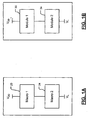
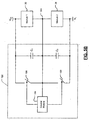
- FIGs. 1A and 1 B are functional block diagrams illustrating stacked complex logic macros and modules, respectively, operating at twice a normal voltage level and half of a normal current level;
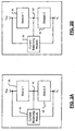
- FIGs. 2A and 2B are functional block diagrams illustrating stacked complex logic macros and modules, respectively, with a current balancing module;
- FIGs. 3A and 3B are functional block diagrams illustrating stacked complex logic macros and modules with balancing provided by a buck converter
- FIGs. 4A and 4B are functional block diagrams illustrating stacked complex logic macros and modules with balancing provided by a 2:1 DC/DG converter;
- FIGs. 5A and 5B are functional block diagrams illustrating stacked complex logic macros and modules with balancing provided by first exemplary balanced switched capacitance devices
- FIGs. 6A and 6B are functional block diagrams illustrating stacked complex logic macros and modules with balancing provided by second exemplary balanced switched capacitance devices
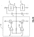
- FIGs. 7A and 7B are functional block diagrams illustrating stacked complex logic macros and modules with balancing provided by a linear push-pull regulator
- FIGs. 8A and 8B are functional block diagrams illustrating stacked logic macros and modules with balancing provided by hysteresis comparators
- FIG. 9A is a functional block diagram illustrating the supply of voltage and current to a module or macro using a DC/DC converter and 2:1 converters according to the prior art
- FIG. 9B is a functional block diagram illustrating the supply of voltage and current to two stacked modules or macros according to some implementations of the present invention.
- FIG. 9C is a functional block diagram illustrating the supply of voltage and current to four stacked modules or macros according to other implementations of the present invention.
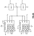
- FIG. 10A is a functional block diagram illustrating a communications device including multiple communications channels each with a signal processor
- FIG. 10B is a functional block diagram illustrating the supply of voltage and current to the communications device of FIG. 10A;
- FIG. 11A is a functional block diagram illustrating a graphics processing unit (GPU) including multiple graphics pipeline modules;
- GPU graphics processing unit
- FIG. 11 B is a functional block diagram illustrating the connection of the supply of voltage and current to the graphics pipeline modules of FIG. 11A;
- FIG. 12 is a functional block diagram illustrating first and second processors, a power adjustment module that balances current dissipation of the first and second processors and an optional current balancing module;
- FIG. 13A is a functional block diagram illustrating first and second processors, a frequency balancing module that reduces a difference between operating frequencies of the first and second processors to reduce current imbalance and an optional 2:1 DC/DC converter;
- FIG. 13B is a functional block diagram illustrating an exemplary layout of the first and second processors and a 2:1 DC/DC converter on a semiconductor die;
- FIG. 13C is a side view illustrating packaging of the semiconductor die of FIG. 13B and external inductors on a PCB;
- FIG. 14 is a functional block diagram illustrating first and second processors, an operating system that balances current dissipation of the first and second processors and an optional current balancing module.
- module or modules refers to an application specific integrated circuit (ASIC), an electronic circuit, a processor (shared, dedicated, or group) and memory that execute one or more software or firmware programs, a microprocessor subsystem, a combinatorial logic circuit, complex logic macros and/or other suitable components that provide the described functionality.
- ASIC application specific integrated circuit
- the present invention stacks groups of devices (such as complex logic macros and/or modules) on top of each other to overcome practical parasitic resistance barriers.
- complex logic macros 20 and 24 are stacked on top of another and connected between V DD and V L .
- V L may be ground.
- modules 30 and 34 are stacked on top of another and connected between V DD and V L . If the complexity of the complex logic macros 20 and 24 or modules 30 and 34 is approximately divided into two equal partitions and if the two halves are run approximately equally, the current requirement will be approximately half of non-stacked devices.
- the stacked devices run at twice the voltage of the unstacked devices. However there is no guarantee that both the complex logic macros 20 and 24 or modules 30 and 34 will consume substantially equal current levels. This may seem to be an impossible problem to solve unless the two halves can be made to draw substantially the same amount of current. There is no way to practically guarantee that two halves will drop half of the total voltage applied to the overall device.
- a current balancing module 50 is connected to at least one of V DD , V L and/or a node 52 between the logic macros 20 and 24 or modules 30 and 34.
- the current balancing module 50 attempts to balance the amount of current supplied to the logic macros 20 and 24 or the modules 30 and 34.
- the current balancing module 50 supplies approximately 1/2 of (V DD - V L ) to each of the complex logic macros 20 and 24 in FIG. 2A or to each of the modules 30 and 34 in FIG. 2B.
- Exemplary current balancing modules 50 include buck converters, 2:1 DC/DC converters, linear push-pull regulators, low drop-out (LDO) regulators, balancing switched capacitance devices, switched inductance devices, capacitance/inductance devices, hysteresis comparators, and/or other similar devices, as will be described further below.
- LDO low drop-out
- the buck converter 68 may have the topology shown in FIGs. 3A and 3B and/or any other suitable topology.
- the buck converter 68 includes a conduction switch 70 and a freewheeling switch 72.
- a control module 73 generates drive signals for the switches 70 and 72.
- the control module 73 may sense voltage and/or current at node 52 and control the switches based thereon.
- the switches 70 and 72 have opposite states.
- An inductance element 78 has one end that is connected between the switches 70 and 72 and an opposite end that is connected between the complex logic macros 20 and 24 or the modules 30 and 34.
- the buck converter 68 sinks or sources current to provide balancing.
- FIGs. 4A and 4B one implementation for balancing the current between the two halves so that the voltages seen by the two halves are approximately equal is shown.
- the balancing act is accomplished by a 2:1 DC/DC converter 100 utilizing a coupled inductor 104. Further operational details are set forth in "Voltage Regulator", U.S. Patent Application Serial No. 10/693,787, filed on October 24, 2003, which is hereby incorporated by reference in its entirety.
- the 2:1 DC/DC converter 100 includes two buck converters operating 180 degrees out of phase to generate an output voltage, V OUT , from an input voltage V DD .
- Each buck converter includes a conduction switch 110a or 110b, a free-wheeling switch 114a or 114b, and an inductor 104a or 104b.
- An output capacitance 118 filters the output voltage for each of the buck converters. The value of the output capacitance 118 may be decreased since there is negligible ripple current.
- any capacitance at the input works in concert with the output capacitance 118 to effectively provide parallel capacitance to a load at the output.
- a control module 119 generates drive signals for the switches 110a, 110b, 114a and 114b. The control module 119 may sense voltage or current at node 52 and control the switches based thereon.
- a startup circuit 130 is optionally provided to ensure that the node 52 is maintained at a voltage that is less than V DD during startup.
- the node is maintained at approximately V DD /2 during startup.
- the startup circuit 130 includes one or more capacitors.
- V DD can be increased or ramped during startup to prevent excess voltage across the modules and to ensure that the node 52 is at least one of maintained at approximately V DD /2 during startup and/or less than a threshold voltage V TH , which is less than V DD .
- the threshold V TH should be less than a voltage that will cause damage to the macros and/or modules.
- the output capacitance 118 o FIG. 4A is labeled 118B.
- Another capacitance 118A can optionally be added to ensure that the macros and/or modules do not receive more than V TH and/or approximately V DD /2 during startup. Alternately, V DD can be increased or ramped during startup to prevent excess voltage across the macros and/or modules. Still other ways of limiting voltage during startup can be used. In some implementations, the capacitance values of the capacitances are set substantially equal.
- the inductors, 104a and 104b may be tightly coupled together and have a coefficient of coupling, K, of approximately one.
- the inductors 104a and 104b may be wound together on a common magnetic core to form an inductor assembly 104 that provides a high coefficient of coupling between the inductors 104a and 104b.
- the polarities of the inductor windings are selected so that the DC currents flowing through the inductors 104a and 104b approximately cancel so that approximately zero DC current flows through the magnetic core of the inductor assembly 104.
- the inductors 104a and 104b may be used for the inductors 104a and 104b, resulting in a smaller size (volume) and lower cost for the inductor assembly 104.
- the transient response of the 2:1 DC/DC converter 100 is improved due to cancellation of the individual inductances as far as transient load currents are concerned.
- the 2:1 DC/DC converter 100 guarantees that the voltages seen by the two halves of the complex logic macros 20 and 24 or modules 30 and 34 are approximately equal. Assuming that the two halves have at most 25% mismatch in current levels, the 2:1 DC/DC converter 100 needs to sink or source 25% of the current of half of the overall device, or 1/8 of the overall current.
- the 2:1 DC/DC converter 100 needs to sink or source current of less than 12.5A. This can easily be made with integrated power MOSFETS within the microprocessor die and a single 1:1 coupled inductor 104 mounted underneath the microprocessor packaging as shown in FIGs. 13A-13C described below.
- the stacking of complex logic macros 20 and 24 or modules 30 and 34 is not only useful for high power semiconductor devices, but also for low power integrated circuits targeted for use in handheld markets such as personal digital assistants (PDA), MP3 players, portable satellite radios, cellular phones, etc.
- PDA personal digital assistants
- MP3 players portable satellite radios
- cellular phones etc.
- DC/DC converters can be used to generate the different low voltage supply levels that are required to operate modern semiconductor devices.
- Stacking complex logic macros 20 and 24 or modules 30 and 34 is suited to applications where two complex logic macros or modules can be operated at low voltages and where the combined stacked voltage is already available to run an analog portion of the integrated circuit.
- a device with a 1.8V analog supply can be used to power two halves of embedded logic running at 0.9V each. Discrepancies in the current between the two halves still need to be handled.
- a balancing switched capacitance device 150 can be used to ping and pong current between the two halves as shown in FIG. 5A and 5B.
- a control module 154 senses current and/or voltage at node 164 and controls switches 158 and 160 to alter the charging and discharging of the capacitors C 1 and C 2 .
- the ping and pong action of the balancing capacitors C 1 and C 2 can be used to guarantee that the voltages of the two halves are approximately equal even if there is an imbalance of the current requirements between the two halves.
- a capacitance value of C 1 is set substantially equal to a capacitance value of C 2 to prevent excess voltage across the modules 20 and 24 during startup.
- node 164 is maintained less than VTH and/or approximately equal to V DD /2 during startup. While a balanced switched capacitance device is shown, skilled artisans will appreciate that switched inductance devices and/or switched capacitance/inductance devices can also be used.
- an alternate balanced switched capacitance device is shown to include capacitors C 1 , C 2 and C 3 , switches 180, 182, 184 and 186.
- a switched capacitor module 192 controls the switches 180-186 to sink or source current from node 192.
- the switches 180 and 184 are switched as a pair and the switches 182 and 186 are also switched as a pair and have the opposite state.
- the switched capacitance module 190 may sense the current or voltage at node 192 and control the switches based thereon.
- the ping and pong action of the balancing capacitors C 1 , C 2 and C 3 can be used to guarantee that the voltages of the two halves are approximately equal even if there is an imbalance of the current requirements between the two halves.
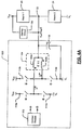
- a linear push-pull regulator 200 can be used with some loss of efficiency. If the two halves are designed to be relatively balanced, the loss of efficiency should be minimal. This approach performs significantly better than linear regulators, which typically have only 50% efficiency. Nonetheless, linear regulators can also be used in some implementations.
- the linear push-pull regulator 200 includes first and second opamps 204 and 208 having outputs that communicate with control terminals of transistors T1 and T2, respectively.
- the transistors T1 and T2 are CMOS transistors.
- a first terminal of the transistor T1 is coupled to V DD .
- a second terminal of the transistor T1 is coupled to a first terminal of transistor T2.
- a second terminal of transistor T2 is coupled to V L .
- a non-inverting input of the opamp 204 is coupled to an upper voltage threshold V UL and a non-inverting input of the opamp 208 is coupled to a lower voltage threshold V LL .
- An inverting input of the opamp 208 is coupled to an inverting input of the opamp 204 and to one end of a resistance R.
- An opposite end of the resistance R is coupled to the second and first terminals of the first and second transistors T1 and T2, respectively.
- the second and first terminals of the first and second transistors T1 and T2, respectively, are also coupled to a node 210 between the first and second logic macros 20 and 24 in FIG. 7A or the first and second modules 30 and 34 in FIG. 7B.
- the upper logic macro or module is dropping too much voltage.
- the upper opamp 204 turns on the transistor T1 momentarily, which applies V DD to node 210.
- V DD at node 210 pulls up the voltage across logic macro or module 24 or 34 and pushes down the voltage across the logic macro or module 20 or 30.
- V DD is applied to node 210, the opamp 204 turns off T1 and the process repeats until the difference is less than the first threshold.
- the lower logic macro or module is dropping too much voltage.
- the lower opamp 208 turns on the transistor T2 momentarily, which applies V L to node 210.
- V L at node 210 pulls up the voltage across logic macro or module 20 or 30 and pushes down the voltage across the logic macro or module 24 or 34.
- V L is applied to node 210, the opamp 208 turns off T2 and the process repeats until the difference is less than the first threshold.
- any type of regulator can be used.
- other types of DC/DC converters, push pull regulators, and switched capacitance devices can be used.
- Still other types of regulators including but not limited to hysteretic comparators can also be used.
- suitable hysteretic comparators include those shown and described in "Simplified Comparator with Digitally Controllable Hysteresis and Bandwidth", U.S. Patent Application Serial No. 10/602,997 filed on June 23, 2003, which is hereby incorporated by reference in its entirety.
- first and second capacitances C 1 and C 2 are provided to limit voltage across the modules 30 and 34 during startup to less than V TH approximately equal to V DD /2 and/or .
- a capacitance value of capacitance C 1 is substantially equal to a capacitance value of C 2 .
- node 210 is maintained at approximately V DD /2 during startup.
- hysteresis comparators 250 and 254 are used to regulate the voltage across the logic macros 20 and 24 or the modules 30 and 34.
- Comparator 250 receives V DD , an upper voltage threshold V UL , and a voltage at node 210.
- the comparator 250 has fixed or adjustable offset 256, bandwidth 258 and/or delay 260. If adjustable, the comparator 254 receives one or more corresponding inputs for making the respective adjustment.
- Comparator 254 receives V L , a lower voltage threshold V LL , and a voltage at node 210.
- the upper logic macro or module is dropping too much voltage.
- the comparator 250 applies V DD to node 210.
- V DD at node 210 pulls up the voltage across logic macro or module 24 or 34 and pushes down the voltage across the logic macro or module 20 or 30.
- V DD is applied to node 210 for a delay period
- the comparator 250 stops applying V DD to node 210. The process repeats until the difference is less than the upper threshold.
- V DD ⁇ V L 2 ⁇ V U L When the node 210 is greater than the target voltage of V DD ⁇ V L 2 by a lower threshold ( V DD ⁇ V L 2 ⁇ V U L ) , the lower logic macro or module is dropping too much voltage.
- the comparator 254 applies V L to node 210.
- V L at node 210 pulls up the voltage across logic macro or module 20 or 30 and pushes down the voltage across the logic macro or module 24 or 34.
- V L is applied to node 210 for a delay period, the comparator 254 stops applying V L to node 210. The process repeats until the difference is less than the lower threshold.
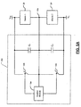
- a DC/DC converter 300 receives an input signal and generates an output at 4V and 25A.
- a first 2:1 converter 304 converts the 4V, 25A input into a 2V, 50A output.
- a second converter 308 converts the 2V, 50A input into a 1V, 100A output.
- a macro or module 312 packaged on a printed circuit board (PCB) 314 may be connected by a resistance 310 (which may represent parasitic resistance of traces and other connections) to the output of the 2:1 converter 308.
- a resistance 310 which may represent parasitic resistance of traces and other connections
- losses due to the parasitic resistance 310 are equal to I 2 R, where I is the current flowing through the parasitic resistance R.
- FIG. 9B the losses can be reduced by a factor of 4 according the present invention by connecting a 2:1 converter 320 (or other current balancing module) between a pair of macros or modules identified at 324 and 328 as discussed above.
- additional modules can be connected with additional 2:1 converters.
- four modules or macros 340, 342, 344 and 346 are connected in series and have nodes 347, 348, and 349 therebetween.
- a first 2:1 converter 330 is connected to the output of the DC/DC converter 300, the macro or module 340 and to node 348.
- the node 348 is also connected to 2:1 converters 334 and 336 and to modules or macros 342 and 344.
- the 2:1 converter 334 is also connected to the output of the DC/DC converter 300, module or macro 340 and nodes 347 and 348 as shown.
- the 2:1 converter 336 is also connected to the nodes 348 and 349 as shown.
- the 2:1 converter 320 can be smaller than the 2:1 converter 308, which handles all of the current flowing to the PCB. In contrast, the 2:1 converter 320 only needs to handle current mismatch between the stacked devices.
- the circuit when it includes 2 n modules or macros, it will include 2 n -1 2:1 DC/DC converters.
- the 2:1 DC/DC converters may be arranged in n branches.
- the 2 n -1 2:1 DC/DC converters have 2 n -1 nodes between adjacent DC/DC converters.
- Each of the 2 n -1 2:1 DC/DC converters are connected to respective ones of the 2 n -1 nodes.
- a communications device 360 such as a router, switch or other network device typically includes multiple communications channels 364-1, 364-2, 364-3 and 364-4 (collectively channels 364). While only four signal processor modules are shown, additional pairs of signal processors can be used. Each channel 364 includes a signal processor 366-1, 366-2, 366-3 and 366-4 (collectively signal processors 366). Since each of the signal-processors 366 typically has the same design, the signal processor modules 366 tend to draw approximately the same amount of current during operation.
- a current balancing module 370 such as those described above or below may be provided to balance differences in current consumption.
- the communications channel can be compliant with 1000Base-T Ethernet, 10GBase-T Ethernet or other current or future Ethernet or other standards.
- a graphics processing unit (GPU) 380 includes multiple graphics pipeline modules 382-1, 382-2, ..., and 382-N (collectively graphics pipeline modules 382). Since each of the graphics pipeline modules 382 have the same design, the graphics pipeline modules 382 tend to draw the same amount of current during operation.
- a current balancing module 390 such as those described above or below may be provided to balance differences in current consumption.
- first and second processors 400 and 402 communicate with a power adjustment module 404 that balances current dissipation of the first and second processors 400 and 402.
- the power adjustment module 404 is hardware-based, software-based, and/or hardware and software based.
- the power adjustment module 404 adjusts relative operating frequencies of the first and second processors to attempt to balance current dissipation.
- the power adjustment module 404 may also use load balancing and/or throttling of the first and second processors 400 and 402 to attempt to balance current dissipation.
- the power adjustment module 404 is used in conjunction with an optional current balancing module 406, as described above and below. In other words, the power adjustment module 404 performs rough balancing and the current balancing module performs fine current balancing.
- the power management module 404 includes a frequency balancing module 404'.
- An optional 2:1 DC/DC converter 406' may also be used to further balance current dissipation.
- FIG. 13B an exemplary layout of the first and second processors 400 and 402 and the 2:1 DC/DC converter 406' are shown fabricated on a semiconductor die 408.
- FIG. 13C the semiconductor die 408 of FIG. 13B is connected to a PCB 412 by first and second sockets 414 and 416 that are arranged on the PCB 412.
- Inductors 420 and 422 that were described above and that are associated with the 2:1 DC/DC converter 406 are arranged between the semiconductor die 408 and the PCB 412 in some embodiments.
- Pins 426 extend from the die 408 and are received in the sockets 414 and 416. While the power management module 404 is shown to include the frequency balancing module 404', skilled artisans will appreciate that hardware and/or software balancing of current may be performed in any of the ways described above and/or below.
- the power adjustment module 404 includes an operating system 404".
- the OS 404" or chip can perform load balancing by assigning threads to the first and second processors 400 and 402.
- the OS 404" or chip can throttle the first and/or second processors 400 and 402 so that current imbalance is small.
- CPU speed can be set as follows: Speed CPU1 or CPU2 1GHz 2GHz 3GHz 4GHz CPU2 or CPU1 0GHz 1 GHz 2GHz 3GHz It is more efficient to run each CPU at 1 ⁇ 2 maximum frequency because each CPU can run at lower voltage.
- an operating frequency of one of the CPUs is lowered and/or increased to balance current dissipation of the other CPU.
- dummy operations can be performed on at least one of the CPUs to balance current imbalance that would otherwise occur.
- circuits and/or capacitors were used to ensure that the voltage at a node between the macros and/or modules is maintained below V TH and/or at approximately V DD /2 during startup. Skilled artisans will appreciate that other implementations shown and described herein can also include the circuits and/or capacitors for maintaining the node between the macros and/or modules below V TH and/or at approximately V DD /2 during startup.
Abstract
Description
- This application is a continuation of U.S. Patent Application No. 11/098,129, filed on April 4, 2005 which claims the benefit of U.S. Provisional Application No. 60/631,552, filed on November 29, 2004 and U.S. Provisional Application No. 60/663,933, filed March 21, 2005. The disclosures of the above applications are incorporated herein by reference in their entirety.
- The present invention relates to the operation of low voltage complex logic macros and/or modules using higher voltage supply levels and lower current levels.
- Complementary metal oxide semiconductor (CMOS) process scaling over the past decade has produced smaller devices through the integration of increasing numbers of transistors. For example, current microprocessors are more than a thousand times more powerful than microprocessors made a decade ago.
- Power dissipation of microprocessors has also increased. Some microprocessors now dissipate more than 100W. Modern processors built using low voltage CMOS processes employ a supply voltage level that barely exceeds 1 V. As a result, CMOS-based microprocessors require current levels that exceed 100A.
- Physical barriers are beginning to limit the amount of current flowing through these devices. One barrier relates to the voltage drop associated with the distribution of power to these microprocessors. A parasitic resistance of 1 mΩ milliohm in chip packaging and/or printed circuit board (PCB) power planes can create 100mV of voltage drop. In reality, it is extremely difficult to lower the parasitic resistance to less than 1 MΩ megaohm without significantly increasing material and associated processing costs.
- For example, the resistance of a gold bond wire in typical semiconductor packaging has a resistance of about 100 MΩ for a 1 micron diameter and 5 mm length. To limit the total power supply resistance to less than 1 MΩ, each power supply connection (VDD and Vss) must be limited to less than 0.5 MΩ. This approach requires more than 400 bond wires. A lot more bondwires will be required due to other sources of parasitic resistance.
- One approach eliminates the bond wires and uses flip chip packaging technology. This approach solves half of the packaging resistance problem. Additional considerations include the resistance of the metal within the semiconductor itself, the metal resistance of the flip chip packaging, and the metal resistance of the printed circuit board (PCB) must also be accommodated. As the chips continue to shrink, the traces of the wiring must be made narrower. As a result, thinner metal material must be used, which in turn increases the parasitic resistances.
- A circuit comprises a first module and a second module that communicates with the first module. The first and second modules are connected in series between first and second reference potentials. A current balancing module communicates with a node between the first and second modules and reduces a difference in current consumption between the first and second modules.
- In other features, the current balancing module comprises a buck converter. The buck converter comprises a conduction switch that communicates with a third reference potential. A freewheeling switch communicates with a fourth reference potential and the conduction switch. An inductance element communicates with the conduction and freewheeling switches and the node. A capacitance element communicates with the fourth reference potential and the node.
- In other features, the current balancing module comprises a 2:1 DC/DC converter. The 2:1 DC/DC converter comprises first and second conduction switches. First and second inductance elements communicate with the first and second conduction switches. First and second freewheeling switches communicate with first and second conduction switches to provide a path for current during non-conduction periods. The 2:1 DC/DC converter further comprises a drive signal generator that generates drive signals that control the first and second conduction switches and freewheeling switches. The first and second inductance elements are wound together on a common core. The first and second conduction switches, the first and second inductance elements, and the first and second freewheeling switches are connected in a buck configuration such that an output voltage is approximately one-half the amplitude of an input voltage.
- In other features, the current balancing module comprises a balanced switched capacitance device. The balanced switched capacitance device comprises a first capacitance element having a first end that communicates with the first module and the first reference potential and a second end that communicates with the node. A second capacitance element has a first end that communicates with the second module and the second reference potential and a second end that communicates with the node. A third capacitance element has first and second ends. A plurality of switches selectively connect and disconnect the first, second and third capacitances to the first and second modules to balance current consumption of the first and second modules. The plurality of switches comprise a first switch having a first end that communicates with the first end of the first capacitance element and a second end that communicates with the first end of the third capacitance element, a second switch having a first end that communicates with the first end of the second capacitance element and a second end that communicates with the second end of the third capacitance element, a third switch having a first end that communicates with the first end of the third capacitance element and a second end that communicates with the node, and a fourth switch having a first end that communicates with the second end of the third capacitance element and a second end that communicates with the node. A drive signal generator generates drive signals that control the plurality of switches.
- In other features, the current balancing module comprises a linear push-pull regulator. The linear push-pull regulator comprises first and second linear push-pull regulators. The first stage of the linear push-pull regulator comprises a first operational amplifier (opamp), a first transistor having a control input that communicates with an output of the first opamp, a first terminal that communicates with a third reference potential, and a second terminal that communicates with the node. The second stage of the linear push-pull regulator comprises a second operational amplifier (opamp), a second transistor having a control input that communicates with an output of the second opamp, a first terminal that communicates with the node, and a second terminal that communicates with a fourth reference potential, and a resistance element having a first end that communicates with first inputs of the first and second opamps and a second end that communicates with the node.
- In still other features, the current balancing module comprises a hysteresis comparator module. The hysteresis comparator module comprises at least one of adjustable offset module, adjustable bandwidth module and/or adjustable delay module. The circuit is an integrated circuit.
- In other features, a DC/DC converter receives an input signal and generates an output signal. A second 2:1 DC/DC converter has an input that communicates with an output of the DC/DC converter and an output that communicates with an input of the 2:1 DC/DC converter.
- In yet other features third and fourth modules are provided. The first, second, third and fourth modules are connected in series between the first and second reference potentials. The current balancing module comprises a first 2:1 DC/DC converter that communicates with the first reference potential, a first node between the first and second modules and a second node between the second and third modules. A second 2:1 DC/DC converter communicates with the second node, a third node between the third and fourth modules and the second reference potential. A third 2:1 DC/DC converter communicates with the first reference potential, the second node and the second reference potential.
- In still other features, a device comprises the circuit and further comprises N pairs of circuits. The first module comprises a first circuit of one of the N pairs of circuits. The second module comprises a second circuit of one of the N pairs of circuits. The N pairs of circuits comprise processing circuits. A third module comprises a first circuit of another of the N pairs of circuits. A fourth module comprises a second circuit of another of the N pairs of circuits. The third and fourth modules are connected in series between the first and second reference potentials and the current balancing module communicates with a node between the third and fourth modules. The first, second, third and fourth modules comprise signal processing modules. The first, second, third and fourth modules comprise graphic pipeline modules.
- In other features, a processing system comprises the device. The first module comprises a first central processing unit (CPU) and the second module comprises a second CPU. An operating system communicates with the first and second CPUs and performs at least one of load balancing and/or throttling of the first and second CPUs to reduce a difference in current consumption between the first and second CPUs.
- In yet other features, the first and second CPUs are both implemented by a single integrated circuit. The current balancing module comprises a 2:1 DC/DC converter including first and second inductors. Components of the 2:1 DC/DC converter other than the first and second inductors are implemented by the integrated circuit.
- In still other features, a system comprises the processing system and further comprises a printed circuit board (PCB), first and second sockets arranged on the PCB, and pins that extend from the integrated circuit and that are received by the first and second sockets. The first and second inductors are attached to the integrated circuit and arranged between the integrated circuit and the PCB.
- A network device comprises a first channel module, a second channel module in series with the first channel module, a third channel module in series with the second channel module, and a fourth channel module in series with the third channel module. The first and fourth modules are connected in series between first and second reference potentials. The first, second, third and fourth channel modules are functionally equivalent.
- In other features, a current balancing module communicates with nodes between the first and second channel modules, the second and third channel modules and the third and fourth channel modules and reduces a difference in current consumption between the first, second, third and fourth channel modules. The network device is 1000Base-T compliant. The network device is 10GBase-T compliant.
- In other features, the current balancing module comprises a buck converter. The current balancing module comprises a 2:1 DC/DC converter. The current balancing module comprises a balanced switched capacitance device. The current balancing module comprises a linear push-pull regulator. The current balancing module comprises a hysteresis comparator module.
- A processing system comprises a first processing module and a second processing module that communicates with the first processing module. The first and second processing modules are connected in series between first and second reference potentials. An operating system communicates with the first and second processing modules and performs at least one of load balancing and/or throttling of the first and second processing modules to reduce a difference in current consumption between the first and second processing modules.
- In other features, a current balancing module communicates with a node between the first and second processing modules and reduces a difference in current consumption between the first and second processing modules.
- In other features, the current balancing module comprises a buck converter. The current balancing module comprises a 2:1 DC/DC converter. The current balancing module comprises a balanced switched capacitance device. The current balancing module comprises a linear push-pull regulator. The current balancing module comprises a hysteresis comparator module. The first and second processing modules comprise first and second graphics pipeline modules.
- The first and second processing modules are both implemented by a single integrated circuit. The current balancing module comprises a 2:1 DC/DC converter including first and second inductors. Components of the 2:1 DC/DC converter other than the first and second inductors are implemented by the integrated circuit.
- A system comprises the processing system and further comprises a printed circuit board (PCB), first and second sockets arranged on the PCB, and pins that extend from the integrated circuit and that are received by the first and second sockets. The first and second inductors are attached to the integrated circuit and arranged between the integrated circuit and the PCB.
- A circuit comprises 2n modules that are connected in series between first and second reference potentials. 2n-1 nodes are arranged between adjacent ones of the 2n modules. 2n-1 2:1 DC/DC converters communicate with a respective one of the 2n-1 nodes.
- In other features, the 2n-1 2:1 DC/DC converters are arranged in n branches. A first branch includes one of the 2n-1 2:1 DC/DC converters, a second branch includes two of the 2n-1 2:1 DC/DC converters, and an nth branch includes 2n-1 of the 2n-1 2:1 DC/DC converters. The modules include complex logic macros. The modules include application specific integrated circuits (ASIC). The modules include processing modules.
- A method comprises performing a first function using a first module; performing a second function using a second module that communicates with the first module; connecting the first and second module in series between first and second reference potentials; and reducing a difference in current consumption between the first and second modules.
- In other features, the method includes performing the reducing step using a buck converter. The method includes performing the reducing step using a 2:1 DC/DC converter. The method includes performing the reducing step using a balanced switched capacitance device. The method includes performing the reducing step using linear push-pull regulating module. The method includes performing the reducing step using hysteresis comparator module.
- A method for operating a network device comprises providing a first communications channel; providing a second communications channel in series with the first communications channel; providing a third communications channel in series with the second communications channel; and providing a fourth communications channel in series with the third communications channel. The first and fourth communications channels are connected in series between first and second reference potentials and wherein the first, second, third and fourth communications channels are functionally equivalent.
- In other features, the method includes reducing a difference in current consumption between the first, second, third and fourth communications channels. The network device is 1000Base-T compliant. The network device is 10GBase-T compliant.
- In other features, the method includes performing the reducing step using a buck converter. The method includes performing the reducing step using a 2:1 DC/DC converter. The method includes performing the reducing step using a balanced switched capacitance device. The method includes performing the reducing step using linear push-pull regulating module. The method includes performing the reducing step using hysteresis comparator module.
- A method comprises providing a first processing module; providing a second processing module that communicates with the first processing module, wherein the first and second processing modules are connected in series between first and second reference potentials; and performing at least one of load balancing and/or throttling of the first and second processing modules to reduce a difference in current consumption between the first and second processing modules.
- In other features, the method includes reducing a difference in current consumption between the first and second processing modules.
- In other features, the method includes performing the reducing step using a buck converter. The method includes performing the reducing step using a 2:1 DC/DC converter. The method includes performing the reducing step using a balanced switched capacitance device. The method includes performing the reducing step using linear push-pull regulating module. The method includes performing the reducing step using hysteresis comparator module.
- The first and second processing modules are both implemented by a single integrated circuit. The 2:1 DC/DC converter includes first and second inductors. Components of the 2:1 DC/DC converter other than the first and second inductors are implemented by the integrated circuit.
- First and second sockets are arranged on a PCB and pins extend from the integrated circuit and are received by the first and second sockets. The first and second inductors are attached to the integrated circuit and arranged between the integrated circuit and the PCB.
- A method comprises providing 2n modules that are connected in series between first and second reference potentials; providing 2n-1 nodes that are arranged between adjacent ones of the 2n modules; and providing 2n-1 2:1 DC/DC converters for converting, wherein each of the 2n-1 2:1 DC/DC converters communicates with a respective one of the 2n-1 nodes.
- In other features, the 2n-1 2:1 DC/DC converters are arranged in n branches. A first branch includes one of the 2n-1 2:1 DC/DC converters, a second branch includes two of the 2n-1 2:1 DC/DC converters, and an nth branch includes 2n-1 of the 2n-1 2:1 DC/DC converters. The 2n modules include complex logic macros. The 2n modules include application specific integrated circuits (ASIC). The 2n modules include processing module.
- A circuit comprises first means for performing a first function and second means for performing a second function and that communicates with the first means. The first and second means are connected in series between first and second reference potentials. Current balancing means communicates with a node between the first and second means and reduces a difference in current consumption between the first and second means.
- In other features, the current balancing means comprises a buck converter. The buck converter comprises conduction switch means for switching that communicates with a third reference potential. Freewheeling switch means for switching communicates with a fourth reference potential and the conduction switch means. Inductance means for providing inductance communicates with the conduction and freewheeling switch means and the node. Capacitance means for providing capacitance communicates with the fourth reference potential and the node.
- In other features, the current balancing means comprises 2:1 DC/DC converting means for converting. The 2:1 DC/DC converting means comprises first and second conduction switch means for switching. First and second inductance means for, providing inductance communicate with the first and second conduction switch means. First and second freewheeling switch means for switching communicate with first and second conduction switch means to provide a path for current during non-conduction periods. The 2:1 DC/DC converting means further comprises drive signal generating means for generating drive signals that control the first and second conduction switch means and freewheeling switch means. The first and second inductance means are wound together on a common core. The first and second conduction switch means, the first and second inductance means, and the first and second freewheeling switch means are connected in a buck configuration such that an output voltage is approximately one-half the amplitude of an input voltage.
- In other features, the current balancing means comprises balanced switched capacitance means for switching capacitance. The balanced switch capacitance means comprises first capacitance means for providing capacitance having a first end that communicates with the first means and the first reference potential and a second end that communicates with the node. Second capacitance means for providing capacitance has a first end that communicates with the second means and the second reference potential and a second end that communicates with the node. Third capacitance means for providing capacitance has first and second ends. A plurality of switch means for switching selectively connect and disconnect the first, second and third capacitance means to the first and second means to balance current consumption of the first and second means. The plurality of switch means comprise first switch means for switching having a first end that communicates with the first end of the first capacitance means and a second end that communicates with the first end of the third capacitance means, second switch means for switching having a first end that communicates with the first end of the second capacitance means and a second end that communicates with the second end of the third capacitance means, third switch means for switching having a first end that communicates with the first end of the third capacitance means and a second end that communicates with the node; and fourth switch means for switching having a first end that communicates with the second end of the third capacitance means and a second end that communicates with the node. Drive signal generating means for generating drive signals controls the plurality of switch means.
- In other features, the current balancing means comprises linear push-pull regulating means for regulating. The linear push-pull regulating means comprises first and second linear push-pull regulators. The first stage of the linear push-pull regulating comprises a first operational amplifier (opamp), a first transistor having a control input that communicates with an output of the first opamp, a first terminal that communicates with a third reference potential, and a second terminal that communicates with the node. The second stage of the linear push-pull regulator comprises a second operational amplifier (opamp), a second transistor having a control input that communicates with an output of the second opamp, a first terminal that communicates with the node, and a second terminal that communicates with a fourth reference potential, and a resistance element having a first end that communicates with first inputs of the first and second opamps and a second end that communicates with the node.
- In yet other features, the current balancing means comprises hysteresis comparator means for balancing current. The hysteresis comparator means comprises at least one of adjustable offset means for adjusting offset, adjustable bandwidth means for adjusting bandwidth and/or adjustable delay means for adjusting delay.
- In other features, the circuit is an integrated circuit. DC/DC converting means for converting receives an input signal and generates an output signal. Second 2:1 DC/DC converting means for converting has an input that communicates with an output of the DC/DC converting means and an output that communicates with an input of the 2:1 DC/DC converting means.
- In other features, the circuit includes third and fourth means for performing third and fourth functions. The first, second, third and fourth means are connected in series between the first and second reference potentials. The current balancing means comprises first 2:1 DC/DC converting means for converting that communicates with the first reference potential, a first node between the first and second means and a second node between the second and third means, second 2:1 DC/DC converting means for converting that communicates with the second node, a third node between the third and fourth means and the second reference potential, and third 2:1 DC/DC converting means for converting that communicates with the first reference potential, the second node and the second reference potential.
- A device comprises the circuit and further comprises N pairs of circuits. The first means comprises a first circuit of one of the N pairs of circuits, and wherein the second means comprises a second circuit of one of the N pairs of circuits. The N pairs of circuits comprise processing means for processing. Third means for performing a third function comprises a first circuit of another of the N pairs of circuits. Fourth means for performing a fourth function comprises a second circuit of another of the N pairs of circuits. The third and fourth means are connected in series between the first and second reference potentials and the current balancing means communicates with a node between the third and fourth means. The first, second, third and fourth means comprise signal processing means for processing.
- In other features, a graphics processing unit (GPU) comprises the device. The first, second, third and fourth means comprise graphic pipeline means for processing graphics.
- In other features, a processing system comprises the device. The first means comprises first processing means for processing and the second means comprises second means for processing. An operating system communicates with the first and second processing means and performs at least one of load balancing and/or throttling of the first and second processing means to reduce a difference in current consumption between the first and second processing means. The first and second processing means are both implemented by a single integrated circuit.
- In still other features, the current balancing means comprises a 2:1 DC/DC converting means for converting including first and second inductance means for providing inductance. Components of the 2:1 DC/DC converting means other than the first and second inductance means are implemented by the integrated circuit. A system comprises the processing system and further comprises a printed circuit board (PCB), first and second sockets arranged on the PCB, and pins that extend from the integrated circuit and that are received by the first and second sockets. The first and second inductance means are attached to the integrated circuit and arranged between the integrated circuit and the PCB.
- A network device comprises first channel means for providing a first communications channel, second channel means for providing a second communications channel in series with the first channel means, third channel means for providing a third communications channel in series with the second channel means, and fourth channel means for providing a fourth communications channel in series with the third channel means. The first and fourth channel means are connected in series between first and second reference potentials and wherein the first, second, third and fourth channel means are functionally equivalent.
- In other features, current balancing means for balancing current communicates with nodes between the first and second channel means, the second and third channel means and the third and fourth channel means and reduces a difference in current consumption between the first, second, third and fourth channel means. The network device is 1000Base-T compliant. The network device is 10GBase-T compliant.
- In other features, the current balancing means comprises a buck converter. The current balancing means comprises 2:1 DC/DC converting means for converting. The current balancing means comprises balanced switched capacitance means for switching capacitance. The current balancing means comprises linear push-pull regulating means for regulating. The current - balancing means comprises hysteresis comparator means for balancing current. The hysteresis comparator means comprises at least one of adjustable offset means for adjusting offset, adjustable bandwidth means for adjusting bandwidth and/or adjustable delay means for adjusting delay.
- A processing system comprises first processing means for processing and second processing means for processing that communicates with the first processing means. The first and second processing means are connected in series between first and second reference potentials. Operating means for providing an operating system communicates with the first and second processing means and performs at least one of load balancing and/or throttling of the first and second processing means to reduce a difference in current consumption between the first and second processing means.
- In other features, current balancing means communicates with a node between the first and second processing means and reduces a difference in current consumption between the first and second processing means.
- In other features, the current balancing means comprises a buck converter. The current balancing means comprises 2:1 DC/DC converting means for converting. The current balancing means comprises balanced switched capacitance means for switching capacitance. The current balancing means comprises linear push-pull regulating means for regulating. The current balancing means comprises hysteresis comparator means for balancing current. The hysteresis comparator means comprises at least one of adjustable offset means for adjusting offset, adjustable bandwidth means for adjusting bandwidth and/or adjustable delay means for adjusting delay. The processing means comprise graphics pipeline means for processing graphics.
- The first and second processing means are both implemented by a single integrated circuit. The current balancing means comprises a 2:1 DC/DC converting means for converting and including first and second inductance means for providing inductance. Components of the 2:1 DC/DC converting means other than the first and second inductance means are implemented by the integrated circuit.
- A system comprises the processing system and further comprises a printed circuit board (PCB), first and second sockets arranged on the PCB, and pins that extend from the integrated circuit and that are received by the first and second sockets. The first and second inductors are attached to the integrated circuit and arranged between the integrated circuit and the PCB.
- A circuit comprises 2n means for performing 2n functions, respectively, that are connected in series between first and second reference potentials, 2n-1 nodes that are arranged between adjacent ones of the 2n means, and 2n-1 2:1 DC/DC converting means for converting. Each of the 2n-1 2:1 DC/DC converting means communicates with a respective one of the 2n-1 nodes.
- In other features, the 2n-1 2:1 DC/DC converting means are arranged in n branches. A first branch includes one of the 2n-1 2:1 DC/DC converting means, a second branch includes two of the 2n-1 2:1 DC/DC converting means, and an nth branch includes 2n-1 of the 2n-1 2:1 DC/DC converting means. The 2n means include complex logic macros, application specific integrated circuits (ASIC), and/or processing means for processing.
- Further areas of applicability of the present invention will become apparent from the detailed description provided hereinafter. It should be understood that the detailed description and specific examples, while indicating the preferred embodiment of the invention, are intended for purposes of illustration only and are not intended to limit the scope of the invention.
- The present invention will become more fully understood from the detailed description and the accompanying drawings, wherein:
- FIGs. 1A and 1 B are functional block diagrams illustrating stacked complex logic macros and modules, respectively, operating at twice a normal voltage level and half of a normal current level;
- FIGs. 2A and 2B are functional block diagrams illustrating stacked complex logic macros and modules, respectively, with a current balancing module;
- FIGs. 3A and 3B are functional block diagrams illustrating stacked complex logic macros and modules with balancing provided by a buck converter;
- FIGs. 4A and 4B are functional block diagrams illustrating stacked complex logic macros and modules with balancing provided by a 2:1 DC/DG converter;
- FIGs. 5A and 5B are functional block diagrams illustrating stacked complex logic macros and modules with balancing provided by first exemplary balanced switched capacitance devices;
- FIGs. 6A and 6B are functional block diagrams illustrating stacked complex logic macros and modules with balancing provided by second exemplary balanced switched capacitance devices;
- FIGs. 7A and 7B are functional block diagrams illustrating stacked complex logic macros and modules with balancing provided by a linear push-pull regulator;
- FIGs. 8A and 8B are functional block diagrams illustrating stacked logic macros and modules with balancing provided by hysteresis comparators;
- FIG. 9A is a functional block diagram illustrating the supply of voltage and current to a module or macro using a DC/DC converter and 2:1 converters according to the prior art;
- FIG. 9B is a functional block diagram illustrating the supply of voltage and current to two stacked modules or macros according to some implementations of the present invention;
- FIG. 9C is a functional block diagram illustrating the supply of voltage and current to four stacked modules or macros according to other implementations of the present invention;
- FIG. 10A is a functional block diagram illustrating a communications device including multiple communications channels each with a signal processor;
- FIG. 10B is a functional block diagram illustrating the supply of voltage and current to the communications device of FIG. 10A;
- FIG. 11A is a functional block diagram illustrating a graphics processing unit (GPU) including multiple graphics pipeline modules;
- FIG. 11 B is a functional block diagram illustrating the connection of the supply of voltage and current to the graphics pipeline modules of FIG. 11A;
- FIG. 12 is a functional block diagram illustrating first and second processors, a power adjustment module that balances current dissipation of the first and second processors and an optional current balancing module;
- FIG. 13A is a functional block diagram illustrating first and second processors, a frequency balancing module that reduces a difference between operating frequencies of the first and second processors to reduce current imbalance and an optional 2:1 DC/DC converter;
- FIG. 13B is a functional block diagram illustrating an exemplary layout of the first and second processors and a 2:1 DC/DC converter on a semiconductor die;
- FIG. 13C is a side view illustrating packaging of the semiconductor die of FIG. 13B and external inductors on a PCB; and
- FIG. 14 is a functional block diagram illustrating first and second processors, an operating system that balances current dissipation of the first and second processors and an optional current balancing module.
- The following description of the preferred embodiment(s) is merely exemplary in nature and is in no way intended to limit the invention, its application, or uses. For purposes of clarity, the same reference numbers will be used in the drawings to identify similar elements. As used herein, the term module or modules refers to an application specific integrated circuit (ASIC), an electronic circuit, a processor (shared, dedicated, or group) and memory that execute one or more software or firmware programs, a microprocessor subsystem, a combinatorial logic circuit, complex logic macros and/or other suitable components that provide the described functionality.
- Referring now to FIGs. 1 A and 1B, the present invention stacks groups of devices (such as complex logic macros and/or modules) on top of each other to overcome practical parasitic resistance barriers. In FIG. 1A,
complex logic macros modules complex logic macros modules - The stacked devices run at twice the voltage of the unstacked devices. However there is no guarantee that both the
complex logic macros modules - Referring now to FiGs. 2A and 2B, a
current balancing module 50 according to the present invention is connected to at least one of VDD, VL and/or anode 52 between thelogic macros modules current balancing module 50 attempts to balance the amount of current supplied to thelogic macros modules current balancing module 50 supplies approximately 1/2 of (VDD - VL) to each of thecomplex logic macros modules current balancing modules 50 include buck converters, 2:1 DC/DC converters, linear push-pull regulators, low drop-out (LDO) regulators, balancing switched capacitance devices, switched inductance devices, capacitance/inductance devices, hysteresis comparators, and/or other similar devices, as will be described further below. - Referring now to FIGs. 3A and 3B, stacked complex logic macros or modules are shown with balancing provided by a
buck converter 68. Thebuck converter 68 may have the topology shown in FIGs. 3A and 3B and/or any other suitable topology. Thebuck converter 68 includes aconduction switch 70 and afreewheeling switch 72. Acontrol module 73 generates drive signals for theswitches control module 73 may sense voltage and/or current atnode 52 and control the switches based thereon. In some implementations, theswitches inductance element 78 has one end that is connected between theswitches complex logic macros modules buck converter 68 sinks or sources current to provide balancing. - Referring now to FIGs. 4A and 4B, one implementation for balancing the current between the two halves so that the voltages seen by the two halves are approximately equal is shown. In FIG. 4A, the balancing act is accomplished by a 2:1 DC/
DC converter 100 utilizing a coupledinductor 104. Further operational details are set forth in "Voltage Regulator", U.S. Patent Application Serial No. 10/693,787, filed on October 24, 2003, which is hereby incorporated by reference in its entirety. - The 2:1 DC/
DC converter 100 includes two buck converters operating 180 degrees out of phase to generate an output voltage, VOUT, from an input voltage VDD. Each buck converter includes aconduction switch switch inductor output capacitance 118 filters the output voltage for each of the buck converters. The value of theoutput capacitance 118 may be decreased since there is negligible ripple current. In addition, due to the tight coupling between the output and the input of the 2:1 DC/DC converter 100, any capacitance at the input works in concert with theoutput capacitance 118 to effectively provide parallel capacitance to a load at the output. Acontrol module 119 generates drive signals for theswitches control module 119 may sense voltage or current atnode 52 and control the switches based thereon. - A
startup circuit 130 is optionally provided to ensure that thenode 52 is maintained at a voltage that is less than VDD during startup. In some implementations, the node is maintained at approximately VDD/2 during startup. In some implementations, thestartup circuit 130 includes one or more capacitors. Alternately, VDD can be increased or ramped during startup to prevent excess voltage across the modules and to ensure that thenode 52 is at least one of maintained at approximately VDD/2 during startup and/or less than a threshold voltage VTH, which is less than VDD. The threshold VTH should be less than a voltage that will cause damage to the macros and/or modules. - In FIG. 4B, the output capacitance 118 o FIG. 4A is labeled 118B. Another
capacitance 118A can optionally be added to ensure that the macros and/or modules do not receive more than VTH and/or approximately VDD/2 during startup. Alternately, VDD can be increased or ramped during startup to prevent excess voltage across the macros and/or modules. Still other ways of limiting voltage during startup can be used. In some implementations, the capacitance values of the capacitances are set substantially equal. - In some implementations, the inductors, 104a and 104b, may be tightly coupled together and have a coefficient of coupling, K, of approximately one. The
inductors inductor assembly 104 that provides a high coefficient of coupling between theinductors inductors inductor assembly 104. Therefore, a smaller core size with a low permeability material may be used for theinductors inductor assembly 104. In addition, the transient response of the 2:1 DC/DC converter 100 is improved due to cancellation of the individual inductances as far as transient load currents are concerned. - Any excess current, whether in to or out of the
node 52 of the stackedcomplex logic macros modules DC converter 100 back into the main power supply with close to 95% efficiency. After startup, the 2:1 DC/DC converter 100 guarantees that the voltages seen by the two halves of thecomplex logic macros modules DC converter 100 needs to sink or source 25% of the current of half of the overall device, or 1/8 of the overall current. - Returning to the microprocessor example with an original current requirement of 100A, the 2:1 DC/
DC converter 100 needs to sink or source current of less than 12.5A. This can easily be made with integrated power MOSFETS within the microprocessor die and a single 1:1 coupledinductor 104 mounted underneath the microprocessor packaging as shown in FIGs. 13A-13C described below. - Other suitable buck converter and 2:1 converter topologies are shown and described in "Voltage Regulator", U.S. Patent Application Serial No. 10/810,452, filed on March 26, 2004, "Voltage Regulator:, U.S. Patent Application Serial No. 10/693,787, filed on October 24, 2003, and "Digital Low Dropout Regulator", U.S. Patent Application Serial No. 10/754,187, filed on January 8, 2004, which are hereby incorporated by reference in their entirety.
- Referring now to FIGs. 5A and 5B, the stacking of
complex logic macros modules - Stacking
complex logic macros modules - In this case, a balancing switched
capacitance device 150 can be used to ping and pong current between the two halves as shown in FIG. 5A and 5B. Acontrol module 154 senses current and/or voltage atnode 164 andcontrols switches modules node 164 is maintained less than VTH and/or approximately equal to VDD/2 during startup. While a balanced switched capacitance device is shown, skilled artisans will appreciate that switched inductance devices and/or switched capacitance/inductance devices can also be used. - Referring now to FIGs. 6A and 6B, an alternate balanced switched capacitance device is shown to include capacitors C1, C2 and C3, switches 180, 182, 184 and 186. A switched
capacitor module 192 controls the switches 180-186 to sink or source current fromnode 192. In some implementations, theswitches switches node 192 and control the switches based thereon. The ping and pong action of the balancing capacitors C1, C2 and C3 can be used to guarantee that the voltages of the two halves are approximately equal even if there is an imbalance of the current requirements between the two halves. - Referring now to FIGs. 7A and 7B, a linear push-
pull regulator 200 can be used with some loss of efficiency. If the two halves are designed to be relatively balanced, the loss of efficiency should be minimal. This approach performs significantly better than linear regulators, which typically have only 50% efficiency. Nonetheless, linear regulators can also be used in some implementations. - The linear push-
pull regulator 200 includes first andsecond opamps opamp 204 is coupled to an upper voltage threshold VUL and a non-inverting input of theopamp 208 is coupled to a lower voltage threshold VLL.- An inverting input of theopamp 208 is coupled to an inverting input of theopamp 204 and to one end of a resistance R. An opposite end of the resistance R is coupled to the second and first terminals of the first and second transistors T1 and T2, respectively. The second and first terminals of the first and second transistors T1 and T2, respectively, are also coupled to anode 210 between the first andsecond logic macros second modules - When the
node 210 is less than the target voltage of

upper opamp 204 turns on the transistor T1 momentarily, which applies VDD tonode 210. VDD atnode 210 pulls up the voltage across logic macro ormodule module node 210, theopamp 204 turns off T1 and the process repeats until the difference is less than the first threshold. - When the
node 210 is greater than the target voltage of

lower opamp 208 turns on the transistor T2 momentarily, which applies VL tonode 210. VL atnode 210 pulls up the voltage across logic macro ormodule module node 210, theopamp 208 turns off T2 and the process repeats until the difference is less than the first threshold. - As can be appreciated, any type of regulator can be used. In addition to the implementations described above, other types of DC/DC converters, push pull regulators, and switched capacitance devices can be used. Still other types of regulators including but not limited to hysteretic comparators can also be used. For example, suitable hysteretic comparators include those shown and described in "Simplified Comparator with Digitally Controllable Hysteresis and Bandwidth", U.S. Patent Application Serial No. 10/602,997 filed on June 23, 2003, which is hereby incorporated by reference in its entirety.
- In FIG. 7B, first and second capacitances C1 and C2 are provided to limit voltage across the
modules node 210 is maintained at approximately VDD/2 during startup. - Referring now to FIGs. 8A and 8B,
hysteresis comparators logic macros modules Comparator 250 receives VDD, an upper voltage threshold VUL, and a voltage atnode 210. In some implementations, thecomparator 250 has fixed or adjustable offset 256,bandwidth 258 and/ordelay 260. If adjustable, thecomparator 254 receives one or more corresponding inputs for making the respective adjustment.Comparator 254 receives VL, a lower voltage threshold VLL, and a voltage atnode 210. - When the
node 210 is less than the target voltage of

comparator 250 applies VDD tonode 210. VDD atnode 210 pulls up the voltage across logic macro ormodule module node 210 for a delay period, thecomparator 250 stops applying VDD tonode 210. The process repeats until the difference is less than the upper threshold. - When the
node 210 is greater than the target voltage of

comparator 254 applies VL tonode 210. VL atnode 210 pulls up the voltage across logic macro ormodule module node 210 for a delay period, thecomparator 254 stops applying VL tonode 210. The process repeats until the difference is less than the lower threshold. - In addition, skilled artisans will appreciated that while two levels of stacking of logic macros and modules are shown, additional levels of stacking may be used. Still other balancing approaches may be used.
- Referring now to FIG. 9A, a DC/
DC converter 300 receives an input signal and generates an output at 4V and 25A. A first 2:1converter 304 converts the 4V, 25A input into a 2V, 50A output. Asecond converter 308 converts the 2V, 50A input into a 1V, 100A output. A macro ormodule 312 packaged on a printed circuit board (PCB) 314 may be connected by a resistance 310 (which may represent parasitic resistance of traces and other connections) to the output of the 2:1converter 308. As can be appreciated, losses due to theparasitic resistance 310 are equal to I2R, where I is the current flowing through the parasitic resistance R. Referring now to FIG. 9B, the losses can be reduced by a factor of 4 according the present invention by connecting a 2:1 converter 320 (or other current balancing module) between a pair of macros or modules identified at 324 and 328 as discussed above. - Referring now to FIG. 9C, additional modules can be connected with additional 2:1 converters. In FIG. 9C, four modules or
macros nodes converter 330 is connected to the output of the DC/DC converter 300, the macro ormodule 340 and tonode 348. Thenode 348 is also connected to 2:1converters macros converter 334 is also connected to the output of the DC/DC converter 300, module ormacro 340 andnodes converter 336 is also connected to thenodes converter 320 can be smaller than the 2:1converter 308, which handles all of the current flowing to the PCB. In contrast, the 2:1converter 320 only needs to handle current mismatch between the stacked devices. - More generally, when the circuit includes 2n modules or macros, it will include 2n-1 2:1 DC/DC converters. The 2:1 DC/DC converters may be arranged in n branches. The 2n-1 2:1 DC/DC converters have 2n-1 nodes between adjacent DC/DC converters. Each of the 2n-1 2:1 DC/DC converters are connected to respective ones of the 2n-1 nodes.
- For example in FIG. 9C, there are two
branches first branch 350 includes one 2:1 converter and the second branch includes two 2:1 DC/DC converters. More generally, the first branch includes 2° = one 2:1 DC/DC converter, the second branch includes 21 = two 2:1 DC/DC converters, the third branch includes 22 = four 2:1 DC/DC converters..., and the nth branch includes 2n-1 2:1 DC/DC converters. - Referring now to FiGs. 10A and 10B, a
communications device 360 such as a router, switch or other network device typically includes multiple communications channels 364-1, 364-2, 364-3 and 364-4 (collectively channels 364). While only four signal processor modules are shown, additional pairs of signal processors can be used. Each channel 364 includes a signal processor 366-1, 366-2, 366-3 and 366-4 (collectively signal processors 366). Since each of the signal-processors 366 typically has the same design, the signal processor modules 366 tend to draw approximately the same amount of current during operation. Acurrent balancing module 370 such as those described above or below may be provided to balance differences in current consumption. Since mismatch will be low, lower efficiency devices such as linear LDO regulators can be used, although other current balancing modules may also be used. For example, the communications channel can be compliant with 1000Base-T Ethernet, 10GBase-T Ethernet or other current or future Ethernet or other standards. - Referring now to FIGs. 11A and 11B, a graphics processing unit (GPU) 380 includes multiple graphics pipeline modules 382-1, 382-2, ..., and 382-N (collectively graphics pipeline modules 382). Since each of the
graphics pipeline modules 382 have the same design, thegraphics pipeline modules 382 tend to draw the same amount of current during operation. Acurrent balancing module 390 such as those described above or below may be provided to balance differences in current consumption. - Referring now to FIG. 12, first and
second processors power adjustment module 404 that balances current dissipation of the first andsecond processors power adjustment module 404 is hardware-based, software-based, and/or hardware and software based. In some implementations, thepower adjustment module 404 adjusts relative operating frequencies of the first and second processors to attempt to balance current dissipation. Thepower adjustment module 404 may also use load balancing and/or throttling of the first andsecond processors power adjustment module 404 is used in conjunction with an optionalcurrent balancing module 406, as described above and below. In other words, thepower adjustment module 404 performs rough balancing and the current balancing module performs fine current balancing. - Referring now to FIGs. 13A, 13B and 13C, the
power management module 404 includes a frequency balancing module 404'. An optional 2:1 DC/DC converter 406' may also be used to further balance current dissipation. In FIG. 13B, an exemplary layout of the first andsecond processors semiconductor die 408. In FIG. 13C, the semiconductor die 408 of FIG. 13B is connected to aPCB 412 by first andsecond sockets 414 and 416 that are arranged on thePCB 412.Inductors DC converter 406 are arranged between the semiconductor die 408 and thePCB 412 in some embodiments.Pins 426 extend from thedie 408 and are received in thesockets 414 and 416. While thepower management module 404 is shown to include the frequency balancing module 404', skilled artisans will appreciate that hardware and/or software balancing of current may be performed in any of the ways described above and/or below. - Referring now to FIG. 14, the
power adjustment module 404 includes anoperating system 404". TheOS 404" or chip can perform load balancing by assigning threads to the first andsecond processors OS 404" or chip can throttle the first and/orsecond processors Speed CPU1 or CPU2 1GHz 2GHz 3GHz 4GHz CPU2 or CPU1 0GHz 1 GHz 2GHz 3GHz - Referring back to FIGs. 4A, 4B, 5A and 7B, circuits and/or capacitors were used to ensure that the voltage at a node between the macros and/or modules is maintained below VTH and/or at approximately VDD/2 during startup. Skilled artisans will appreciate that other implementations shown and described herein can also include the circuits and/or capacitors for maintaining the node between the macros and/or modules below VTH and/or at approximately VDD/2 during startup.
- Those skilled in the art can now appreciate from the foregoing description that the broad teachings of the present invention can be implemented in a variety of forms. Therefore, while this invention has been described in connection with particular examples thereof, the true scope of the invention should not be so limited since other modifications will become apparent to the skilled practitioner upon a study of the drawings, the specification and the following claims.
Claims (4)
- A network device comprising:a first channel module;a second channel module in series with said first channel module,a third channel module in series with said second channel module; anda fourth channel module in series with said third channel module,wherein said first and fourth modules are connected in series between first and second reference potentials and wherein said first, second, third and fourth channel modules are functionally equivalent.
- The network device of Claim 1 comprising a current balancing module that communicates with nodes between said first and second channel modules, said second and third channel modules and said third and fourth channel modules and that reduces a difference in current consumption between said first, second, third and fourth channel modules.
- The network device of Claim 1 wherein said network device is 1000Base-T compliant.
- The network device of Claim 1 wherein said network device is 10GBase-T compliant.
Applications Claiming Priority (4)
| Application Number | Priority Date | Filing Date | Title |
|---|---|---|---|
| US63155204P | 2004-11-29 | 2004-11-29 | |
| US66393305P | 2005-03-21 | 2005-03-21 | |
| US11/098,129 US7594127B2 (en) | 2004-11-29 | 2005-04-04 | Low voltage logic operation using higher voltage supply levels |
| US11/179,904 US7788510B2 (en) | 2004-11-29 | 2005-07-12 | Low voltage logic operation using higher voltage supply levels |
Publications (3)
| Publication Number | Publication Date |
|---|---|
| EP1662645A2 true EP1662645A2 (en) | 2006-05-31 |
| EP1662645A3 EP1662645A3 (en) | 2008-05-28 |
| EP1662645B1 EP1662645B1 (en) | 2017-01-18 |
Family
ID=36021844
Family Applications (1)
| Application Number | Title | Priority Date | Filing Date |
|---|---|---|---|
| EP05025065.3A Active EP1662645B1 (en) | 2004-11-29 | 2005-11-16 | Low voltage logic operation using higher voltage supply levels |
Country Status (4)
| Country | Link |
|---|---|
| US (1) | US7788510B2 (en) |
| EP (1) | EP1662645B1 (en) |
| JP (1) | JP5095099B2 (en) |
| TW (1) | TWI400866B (en) |
Families Citing this family (8)
| Publication number | Priority date | Publication date | Assignee | Title |
|---|---|---|---|---|
| US8618788B2 (en) * | 2007-03-30 | 2013-12-31 | Malay Trivedi | Dynamically adjusted multi-phase regulator |
| JP5173503B2 (en) | 2008-03-14 | 2013-04-03 | キヤノン株式会社 | Imaging apparatus and imaging system |
| JP5077069B2 (en) * | 2008-05-27 | 2012-11-21 | 株式会社デンソー | Circuit system and power supply voltage control method for circuit system |
| US9891043B2 (en) | 2011-10-11 | 2018-02-13 | Nikon Corporation | Profile measuring apparatus, structure manufacturing system, method for measuring profile, method for manufacturing structure, and non-transitory computer readable medium |
| KR102107076B1 (en) * | 2013-12-02 | 2020-05-08 | 에스케이하이닉스 주식회사 | Semiconductor apparatus |
| US9660627B1 (en) | 2016-01-05 | 2017-05-23 | Bitfury Group Limited | System and techniques for repeating differential signals |
| US9645604B1 (en) | 2016-01-05 | 2017-05-09 | Bitfury Group Limited | Circuits and techniques for mesochronous processing |
| US9514264B1 (en) | 2016-01-05 | 2016-12-06 | Bitfury Group Limited | Layouts of transmission gates and related systems and techniques |
Citations (3)
| Publication number | Priority date | Publication date | Assignee | Title |
|---|---|---|---|---|
| EP0721137A1 (en) * | 1994-07-14 | 1996-07-10 | Seiko Epson Corporation | Power source circuit, liquid crystal display device, and electronic device |
| FR2800955A1 (en) * | 1999-11-04 | 2001-05-11 | Cit Alcatel | Remote power supply for telecommunications terminal has impedance checking procedure avoids damage to incompatible units. |
| US20030095560A1 (en) * | 2001-11-20 | 2003-05-22 | Hiroshi Arita | Packet communication device, packet communication system, packet communication module, data processor, and data transfer system |
Family Cites Families (22)
| Publication number | Priority date | Publication date | Assignee | Title |
|---|---|---|---|---|
| JPS6365760A (en) * | 1986-09-06 | 1988-03-24 | Nec Corp | Calling current supply circuit |
| SE8605266L (en) * | 1986-12-09 | 1988-06-10 | Ragnar Jonsson | SWITCH CONNECTION |
| JPH02114306A (en) * | 1988-10-25 | 1990-04-26 | Mitsubishi Electric Corp | Constant voltage power supply circuit |
| US5204809A (en) * | 1992-04-03 | 1993-04-20 | International Business Machines Corporation | H-driver DC-to-DC converter utilizing mutual inductance |
| US5592069A (en) * | 1992-10-07 | 1997-01-07 | Dallas Semiconductor Corporation | Battery charger |
| JP3694053B2 (en) * | 1994-03-05 | 2005-09-14 | エステイーシー・サブマリン・システムズ・リミテッド | Branch device for submarine communication system |
| US5631534A (en) * | 1995-08-21 | 1997-05-20 | Delco Electronics Corp. | Bidirectional current pump for battery charge balancing |
| JPH10163842A (en) * | 1996-11-25 | 1998-06-19 | Fujitsu Ltd | Semiconductor integrated circuit |
| GB2374991B (en) | 1998-05-07 | 2002-12-18 | Ford Motor Co | Battery charge balancing system |
| JP2000116025A (en) * | 1998-10-06 | 2000-04-21 | Hitachi Ltd | Recharging device |
| US20030135294A1 (en) * | 1998-10-09 | 2003-07-17 | Lam Peter Ar-Fu | Sound generation IC chip set |
| JP2001292529A (en) * | 2000-04-07 | 2001-10-19 | Casio Comput Co Ltd | Charger |
| US6362986B1 (en) * | 2001-03-22 | 2002-03-26 | Volterra, Inc. | Voltage converter with coupled inductive windings, and associated methods |
| US6509725B1 (en) * | 2001-11-09 | 2003-01-21 | International Business Machines Corporation | Self-regulating voltage divider for series-stacked voltage rails |
| JP2006524980A (en) | 2003-04-25 | 2006-11-02 | マックスウェル テクノロジーズ, インク | Charge balancing circuit for double layer capacitor |
| US7872454B2 (en) * | 2003-08-21 | 2011-01-18 | Marvell World Trade Ltd. | Digital low dropout regulator |
| US7760525B2 (en) * | 2003-08-21 | 2010-07-20 | Marvell World Trade Ltd. | Voltage regulator |
| US7085943B2 (en) * | 2003-09-26 | 2006-08-01 | Freescale Semiconductor, Inc. | Method and circuitry for controlling supply voltage in a data processing system |
| US8324872B2 (en) * | 2004-03-26 | 2012-12-04 | Marvell World Trade, Ltd. | Voltage regulator with coupled inductors having high coefficient of coupling |
| US7293181B2 (en) * | 2004-06-28 | 2007-11-06 | Emc Corporation | Use of one voltage regulator module to support two processors to improve power and thermal limitations |
| US7702929B2 (en) * | 2004-11-29 | 2010-04-20 | Marvell World Trade Ltd. | Low voltage logic operation using higher voltage supply levels |
| US7594127B2 (en) * | 2004-11-29 | 2009-09-22 | Marvell World Trade Ltd. | Low voltage logic operation using higher voltage supply levels |
-
2005
- 2005-07-12 US US11/179,904 patent/US7788510B2/en active Active
- 2005-11-16 EP EP05025065.3A patent/EP1662645B1/en active Active
- 2005-11-16 JP JP2005332226A patent/JP5095099B2/en active Active
- 2005-11-17 TW TW094140474A patent/TWI400866B/en not_active IP Right Cessation
Patent Citations (3)
| Publication number | Priority date | Publication date | Assignee | Title |
|---|---|---|---|---|
| EP0721137A1 (en) * | 1994-07-14 | 1996-07-10 | Seiko Epson Corporation | Power source circuit, liquid crystal display device, and electronic device |
| FR2800955A1 (en) * | 1999-11-04 | 2001-05-11 | Cit Alcatel | Remote power supply for telecommunications terminal has impedance checking procedure avoids damage to incompatible units. |
| US20030095560A1 (en) * | 2001-11-20 | 2003-05-22 | Hiroshi Arita | Packet communication device, packet communication system, packet communication module, data processor, and data transfer system |
Also Published As
| Publication number | Publication date |
|---|---|
| US7788510B2 (en) | 2010-08-31 |
| EP1662645A3 (en) | 2008-05-28 |
| JP2006180689A (en) | 2006-07-06 |
| TW200644392A (en) | 2006-12-16 |
| TWI400866B (en) | 2013-07-01 |
| EP1662645B1 (en) | 2017-01-18 |
| US20060114027A1 (en) | 2006-06-01 |
| JP5095099B2 (en) | 2012-12-12 |
Similar Documents
| Publication | Publication Date | Title |
|---|---|---|
| EP1662646B1 (en) | Low voltage logic operation using higher voltage supply levels | |
| US7788509B2 (en) | Low voltage logic operation using higher voltage supply levels | |
| EP1662645B1 (en) | Low voltage logic operation using higher voltage supply levels | |
| US9318952B2 (en) | Series and parallel hybrid switched capacitor networks for IC power delivery | |
| EP2652865B1 (en) | Dual-stage power conversion | |
| Nguyen et al. | High-efficiency fully integrated switched-capacitor voltage regulator for battery-connected applications in low-breakdown process technologies | |
| CN1812236B (en) | Low voltage logic operation using higher voltage supply levels | |
| US11855539B2 (en) | Power module | |
| Viraj et al. | A monolithic cmos 5v/1v switched capacitor dc-dc step-down converter | |
| KR102246854B1 (en) | Matrix switch and power converter using the same | |
| US5880945A (en) | Power conversion and load circuit on same integrated circuit | |
| JPH01218052A (en) | Lsi package | |
| ITO | Research on Highly Efficient and Highly Integrated DC-DC Converters Using Vertical Body Channel MOS Field-Effect Transistor and its Power Management for Microprocessors | |
| JP2022120658A (en) | Flying capacitor circuit and power conversion device |
Legal Events
| Date | Code | Title | Description |
|---|---|---|---|
| PUAI | Public reference made under article 153(3) epc to a published international application that has entered the european phase |
Free format text: ORIGINAL CODE: 0009012 |
|
| AK | Designated contracting states |
Kind code of ref document: A2 Designated state(s): AT BE BG CH CY CZ DE DK EE ES FI FR GB GR HU IE IS IT LI LT LU LV MC NL PL PT RO SE SI SK TR |
|
| AX | Request for extension of the european patent |
Extension state: AL BA HR MK YU |
|
| PUAL | Search report despatched |
Free format text: ORIGINAL CODE: 0009013 |
|
| AK | Designated contracting states |
Kind code of ref document: A3 Designated state(s): AT BE BG CH CY CZ DE DK EE ES FI FR GB GR HU IE IS IT LI LT LU LV MC NL PL PT RO SE SI SK TR |
|
| AX | Request for extension of the european patent |
Extension state: AL BA HR MK YU |
|
| 17P | Request for examination filed |
Effective date: 20081104 |
|
| AKX | Designation fees paid |
Designated state(s): DE FR GB |
|
| 17Q | First examination report despatched |
Effective date: 20090202 |
|
| REG | Reference to a national code |
Ref country code: DE Ref legal event code: R079 Ref document number: 602005051172 Country of ref document: DE Free format text: PREVIOUS MAIN CLASS: H02M0003158000 Ipc: G06F0001260000 |
|
| GRAP | Despatch of communication of intention to grant a patent |
Free format text: ORIGINAL CODE: EPIDOSNIGR1 |
|
| RIC1 | Information provided on ipc code assigned before grant |
Ipc: G06F 1/26 20060101AFI20160721BHEP Ipc: H02J 1/08 20060101ALI20160721BHEP Ipc: H02M 3/158 20060101ALI20160721BHEP |
|
| INTG | Intention to grant announced |
Effective date: 20160818 |
|
| GRAS | Grant fee paid |
Free format text: ORIGINAL CODE: EPIDOSNIGR3 |
|
| GRAA | (expected) grant |
Free format text: ORIGINAL CODE: 0009210 |
|
| AK | Designated contracting states |
Kind code of ref document: B1 Designated state(s): DE FR GB |
|
| REG | Reference to a national code |
Ref country code: GB Ref legal event code: FG4D |
|
| REG | Reference to a national code |
Ref country code: DE Ref legal event code: R081 Ref document number: 602005051172 Country of ref document: DE Owner name: MARVELL ASIA PTE, LTD., SG Free format text: FORMER OWNER: MARVELL WORLD TRADE LTD., ST. MICHAEL, BB |
|
| REG | Reference to a national code |
Ref country code: DE Ref legal event code: R096 Ref document number: 602005051172 Country of ref document: DE |
|
| REG | Reference to a national code |
Ref country code: DE Ref legal event code: R097 Ref document number: 602005051172 Country of ref document: DE |
|
| PLBE | No opposition filed within time limit |
Free format text: ORIGINAL CODE: 0009261 |
|
| STAA | Information on the status of an ep patent application or granted ep patent |
Free format text: STATUS: NO OPPOSITION FILED WITHIN TIME LIMIT |
|
| REG | Reference to a national code |
Ref country code: FR Ref legal event code: PLFP Year of fee payment: 13 |
|
| 26N | No opposition filed |
Effective date: 20171019 |
|
| PGFP | Annual fee paid to national office [announced via postgrant information from national office to epo] |
Ref country code: FR Payment date: 20201126 Year of fee payment: 16 |
|
| REG | Reference to a national code |
Ref country code: DE Ref legal event code: R082 Ref document number: 602005051172 Country of ref document: DE Representative=s name: GRUENECKER PATENT- UND RECHTSANWAELTE PARTG MB, DE Ref country code: DE Ref legal event code: R081 Ref document number: 602005051172 Country of ref document: DE Owner name: MARVELL ASIA PTE, LTD., SG Free format text: FORMER OWNER: MARVELL WORLD TRADE LTD., ST. MICHAEL, BB |
|
| REG | Reference to a national code |
Ref country code: GB Ref legal event code: 732E Free format text: REGISTERED BETWEEN 20210805 AND 20210811 |
|
| PG25 | Lapsed in a contracting state [announced via postgrant information from national office to epo] |
Ref country code: FR Free format text: LAPSE BECAUSE OF NON-PAYMENT OF DUE FEES Effective date: 20211130 |
|
| P01 | Opt-out of the competence of the unified patent court (upc) registered |
Effective date: 20230508 |
|
| PGFP | Annual fee paid to national office [announced via postgrant information from national office to epo] |
Ref country code: GB Payment date: 20231121 Year of fee payment: 19 |
|
| PGFP | Annual fee paid to national office [announced via postgrant information from national office to epo] |
Ref country code: DE Payment date: 20231127 Year of fee payment: 19 |