EP1662642A2 - Highly efficient photoflash diodes driving circuit using low and fixed drop-out current sink - Google Patents
Highly efficient photoflash diodes driving circuit using low and fixed drop-out current sink Download PDFInfo
- Publication number
- EP1662642A2 EP1662642A2 EP05015930A EP05015930A EP1662642A2 EP 1662642 A2 EP1662642 A2 EP 1662642A2 EP 05015930 A EP05015930 A EP 05015930A EP 05015930 A EP05015930 A EP 05015930A EP 1662642 A2 EP1662642 A2 EP 1662642A2
- Authority
- EP
- European Patent Office
- Prior art keywords
- current
- diode
- coupled
- feedback signal
- driving circuit
- Prior art date
- Legal status (The legal status is an assumption and is not a legal conclusion. Google has not performed a legal analysis and makes no representation as to the accuracy of the status listed.)
- Withdrawn
Links
Images


Classifications
-
- H—ELECTRICITY
- H02—GENERATION; CONVERSION OR DISTRIBUTION OF ELECTRIC POWER
- H02J—CIRCUIT ARRANGEMENTS OR SYSTEMS FOR SUPPLYING OR DISTRIBUTING ELECTRIC POWER; SYSTEMS FOR STORING ELECTRIC ENERGY
- H02J7/00—Circuit arrangements for charging or depolarising batteries or for supplying loads from batteries
-
- H—ELECTRICITY
- H05—ELECTRIC TECHNIQUES NOT OTHERWISE PROVIDED FOR
- H05B—ELECTRIC HEATING; ELECTRIC LIGHT SOURCES NOT OTHERWISE PROVIDED FOR; CIRCUIT ARRANGEMENTS FOR ELECTRIC LIGHT SOURCES, IN GENERAL
- H05B45/00—Circuit arrangements for operating light-emitting diodes [LED]
- H05B45/40—Details of LED load circuits
- H05B45/44—Details of LED load circuits with an active control inside an LED matrix
- H05B45/46—Details of LED load circuits with an active control inside an LED matrix having LEDs disposed in parallel lines
-
- H—ELECTRICITY
- H02—GENERATION; CONVERSION OR DISTRIBUTION OF ELECTRIC POWER
- H02J—CIRCUIT ARRANGEMENTS OR SYSTEMS FOR SUPPLYING OR DISTRIBUTING ELECTRIC POWER; SYSTEMS FOR STORING ELECTRIC ENERGY
- H02J7/00—Circuit arrangements for charging or depolarising batteries or for supplying loads from batteries
- H02J7/02—Circuit arrangements for charging or depolarising batteries or for supplying loads from batteries for charging batteries from ac mains by converters
- H02J7/04—Regulation of charging current or voltage
-
- H—ELECTRICITY
- H05—ELECTRIC TECHNIQUES NOT OTHERWISE PROVIDED FOR
- H05B—ELECTRIC HEATING; ELECTRIC LIGHT SOURCES NOT OTHERWISE PROVIDED FOR; CIRCUIT ARRANGEMENTS FOR ELECTRIC LIGHT SOURCES, IN GENERAL
- H05B45/00—Circuit arrangements for operating light-emitting diodes [LED]
- H05B45/30—Driver circuits
- H05B45/345—Current stabilisation; Maintaining constant current
-
- H—ELECTRICITY
- H05—ELECTRIC TECHNIQUES NOT OTHERWISE PROVIDED FOR
- H05B—ELECTRIC HEATING; ELECTRIC LIGHT SOURCES NOT OTHERWISE PROVIDED FOR; CIRCUIT ARRANGEMENTS FOR ELECTRIC LIGHT SOURCES, IN GENERAL
- H05B45/00—Circuit arrangements for operating light-emitting diodes [LED]
- H05B45/30—Driver circuits
- H05B45/37—Converter circuits
- H05B45/3725—Switched mode power supply [SMPS]
- H05B45/38—Switched mode power supply [SMPS] using boost topology
-
- Y—GENERAL TAGGING OF NEW TECHNOLOGICAL DEVELOPMENTS; GENERAL TAGGING OF CROSS-SECTIONAL TECHNOLOGIES SPANNING OVER SEVERAL SECTIONS OF THE IPC; TECHNICAL SUBJECTS COVERED BY FORMER USPC CROSS-REFERENCE ART COLLECTIONS [XRACs] AND DIGESTS
- Y02—TECHNOLOGIES OR APPLICATIONS FOR MITIGATION OR ADAPTATION AGAINST CLIMATE CHANGE
- Y02B—CLIMATE CHANGE MITIGATION TECHNOLOGIES RELATED TO BUILDINGS, e.g. HOUSING, HOUSE APPLIANCES OR RELATED END-USER APPLICATIONS
- Y02B20/00—Energy efficient lighting technologies, e.g. halogen lamps or gas discharge lamps
- Y02B20/30—Semiconductor lamps, e.g. solid state lamps [SSL] light emitting diodes [LED] or organic LED [OLED]
Definitions
- the present invention relates to the field of drivers for photoflash diodes, and more particularly to the field of drivers for photoflash diodes using current sink with low and fixed drop-out voltage. Specifically, the present invention relates to the circuits and control methods that are used for driving photoflash diodes in portable battery devices.
- Portable battery devices drive photoflash diodes using a controller to coordinate the use of the battery power.
- Existing solutions drive the photodiodes from a fixed voltage and then control the diode current through a controlled current sink or current source. However, at low diode current most of the power is wasted through the current sink.
- photoflash diodes are driven using one or more current sinks with a low and fixed drop-out voltage.
- the diodes are driven from a boost or buckboost controller. This forces the current sink drop-out voltage to a very low value through a closed loop feed back system.
- the present invention provides a circuit for driving a photoflash diode.
- the circuit according to the present invention comprises a photoflash diode, a current sink, a feedback circuit, and a DC-DC converter.
- the current sink is coupled to the photoflash diode for controlling the current through the photoflash diode.
- the feedback circuit receives a feedback signal indicative of the electrical condition of said first current regulator.
- the DC-DC converter is coupled to an external power source and the feedback circuit for powering the photoflash diode so as to control the electrical condition of the current sink to a predetermined value.
- FIG. 1 is a block diagram of a photoflash driving circuit according to an embodiment of the present invention.
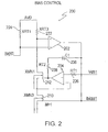
- FIG. 2 is a block diagram of a bias controller according to an embodiment of the present invention.
- FIG. 3 is a block diagram of a current DAC according to an embodiment of the present invention.
- FIG. 4 is a block diagram of a voltage selecting logic circuit according to an embodiment of the present invention.
- FIG. 5 is a block diagram of a error amplifier block according to an embodiment of the present invention.
- FIG. 6 is the diagram showing a method for driving a plurality of photoflash diodes according to an embodiment of the present invention.
- a photoflash driving circuit 100 is illustrated.
- the photoflash driving circuit 100 is used to drive three photoflash diodes 101, 102, and 103. It will be apparent to those skilled in the art that the three photoflash diodes 101, 102, and 103 may be a red, green, and blue photoflash diodes, respectively, for being served as a white light source. Further, the photoflash driving circuit 100 may be used to drive one or more photoflash diodes. It should be understood that the driving circuit 100 can also be used to drive one or more diodes.
- An input voltage source is coupled to a DC-DC converter, such as a boost or buckboost 110, which is coupled to the photoflash diodes 101, 102, and 103 so as to provide a voltage to drive the photoflash diodes 101, 102, and 103.
- a DC-DC converter such as a boost or buckboost 110
- N-type MOSFETs metal-oxide semiconductor field-effect transistor
- the drains of the N-type MOSFETs 121, 122, and 123 are coupled to the photoflash diodes 101, 102, and 103, respectively, and the sources of the N-type MOSFETs 121, 122, and 123 are coupled to ground.
- the gates of the N-type MOSFETs 121, 122, and 123 are coupled to three bias controllers 131, 132, and 133, respectively.
- the voltage signal, Vds1, Vds2, and Vds3 of the drains of the MOSFETs 121, 122, and 123 are input into the bias controllers 131, 132, and 133.
- An I2C controller 146 is coupled to three current DACs (Digital-to-Analog Converter) 141, 142, and 143, which are coupled to the bias controllers 131, 132, and 133, respectively.
- the photoflash driving circuit 100 can be modified to use three P-type MOSFETs served as current sources in place of the current sinks 121, 122, 123.
- Two current control signals, clock (Scl) and data (Sdata), are input into the 12C controller 146 such that the 12C controller provides current setting information, for example, of 3 bits to the current DACs 141, 142, and 143. Based on the current setting information, the current DACs 141, 142, and 143 will generate three current signals, Iset1, Iset2, and Iset3, which are transmitted to the bias controllers 131, 132, and 133, respectively.
- the bias controllers 131, 132, and 133 control the drain currents of the current sinks 121, 122, and 123, i.e., the sink currents.
- Feedback signals such as the voltages of the drains of the current sinks 121, 122, and 123, are input into the bias controllers 131, 132, and 133.
- the bias controllers 131, 132, and 133 provide voltages applied to the gate of the MOSFETs 121, 122, and 123 in accordance with the current signals of the current DACs 141, 143, and 143 and the voltages of the drains of the current sinks 121, 122, and 123 so as to sink the precise amount of current and thus control the brightness of the photoflash diodes 101, 102, and 103.
- the voltages of the drains of the MOSFETs 121, 122, and 123 are input into a voltage selecting logic circuit 160.
- a voltage set signal (Vset) is the voltage set for the drop-out voltage, and is also input into the voltage selecting logic circuit 160.
- the voltage selecting logic circuit 160 is used to select a lowest voltage from the voltages of the drains of the MOSFETs 121, 122, and 123. This lowest voltage and the voltage set signal will be processed at the same procedure in the voltage selecting logic circuit 160 such that the voltage selecting logic circuit 160 generates a lowest voltage signal, S_out1, corresponding to the lowest voltage and a set voltage signal, S_out2, corresponding to the set voltage.
- Both the lowest voltage signal and the set voltage signal are input into an error amplifier block 150.
- the error amplifier block 150 amplifies the error voltage between the lowest voltage signal and the set voltage signal.
- the error amplifier block 150 has a pin (EA-out) coupled to an external capacitor and resistor network 152 for compensating the output (EA) of the error amplifier block 150, i.e., for compensating the amplified voltage.
- the capacitor and resistor network also doubles up as a self-start due to the slewing of rate of voltage charging and discharging.
- the error amplifier block 150 is further provided with a limitation input.
- the limitation input can be a limitation voltage, such as 1.88 volts as shown, to limit the output voltage level of the error amplifier block 150 to the limitation voltage, 1.88 volts.
- the output of the error amplifier block 150 is input into the boost/buckboost 110 for being served as a voltage feedback signal for controlling the output voltage of the boost/buckboost 110.
- the output voltage of the boost/buckboost 110 is used to drive the photoflash diodes 101, 102, and 103.
- the output voltage of the photoflash diodes 101, 102, and 103 or the drop-out voltages of the current sinks 121, 122, and 123, i.e, the drain voltages of the MOSFET 121, 122, and 123, will be sampled into the voltage selecting logic circuit 160 and then to the error amplifier block 150 for generating the voltage feedback signal.
- the drain voltages of the MOSFET 121, 122, and 123 will be forced to the voltage set by the voltage set signal, Vset, for example, 0.1 volts.
- an exemplary bias controller 200 according to an embodiment of the present invention is illustrated and may be used in the photoflash driving circuit 100 as the bias controller 131, 132, or 133.
- the current signal, Iset, from the current DAC is input into the bias controller 200 for setting the current value.
- the bias controller 200 is used in the photoflash driving circuit 100 as the bias controller 131.
- the voltage of the drain of the MOSFET 121, Vds1 is sampled into the op amp 204 through a resistor 226.
- the output of the op amp 204 is coupled to the gate of a MOSFET 212 and the drain of the MOSFET 210 is coupled to the input of the op amp 204 such that the voltage of the drain of the MOSFET 210 is forced to the drain voltage of the MOSFET 121.
- the drain voltage of the MOSFET 121 approaches the set voltage, such as 0.1 volts, which is considerably low, so that the MOSFET 121 and the MOSFET 210 will be operate in the triode or linear region.
- an input of an op amp (operational amplifier) 202 of the bias controller 200 is coupled to the current signal, Iset, and another input of the op amp 202 is coupled to the Iset signal through two resistors 222 and 224.
- a resistor 238 and a capacitor 236 are coupled between the output of the op amp 202 and the output of the op amp 204 for compensating both the op amp 202 and the op amp 204.
- the output of the op amp 202 is coupled to the gate of the N-type MOSFET 210.
- the drain current of the MOSFET 210 is forced by the op amp 202 to the set current.
- the gate of the MOSFET 210 is coupled to one of the gate of the current sinks 121 so as to form a current mirror, in accordance with one embodiment of the present invention.
- the drain current of the current sink 121 is proportional to the drain-source circuit of a MOSFET 210. For example, if the MOSFET 121 is 500 times as large as the MOSFET 210, the drain current of the MOSFET 121 will be 500 times as large as that of the MOSFET 210, i.e., the set current.
- an exemplary current DAC 300 is illustrated and may be used in the photoflash driving circuit 100 as the current DACs 141, 142, or 143.
- the current setting information is input into a decoder 310 of the current DAC 300.
- the current setting information is formed of 3-bit digital information.
- the current DAC 300 further has eight switches 314 and eight current sources 312 respectively coupled to the eight switches 314, respectively.
- the current setting information is decoded by the decoder 310 so as to individually turn on or off eight switches 314 and generate the current signal, Iset1.
- the current signal is the sum of the current of the current source or sources 312 of which the switch 312 is turned on.
- an exemplary voltage selecting logic circuit 400 according to an embodiment of the present invention is illustrated and may be used in the photoflash driving circuit 100 as the voltage selecting logic circuit 160.
- the voltage selecting logic circuit 400 comprises a current source 410, three P-type MOSFET 412, 414, and 416, three transistors 421, 422, and 423, and a set voltage transistor 428.
- the base of the set voltage transistor 428 is coupled the voltage set signal, Vset, and the bases of the three transistors 421, 422, and 423 are coupled to the drains of the MOSFETs 121, 122, and 123, respectively.
- the lowest voltage signal, S_outl, which is corresponding to the lowest voltage is equal to the base-emitter voltage of the transistor 421, 422 or 423 plus the lowest voltage in the voltages of the drains of the MOSFETs 121, 122, and 123.
- the set voltage, S_out2 is equal to the base-emitter voltage of the transistor 428 plus the voltage of voltage set signal. It should be understood that the MOSFET 414 and 416 is used for current match, and the size of the transistor 428 is three times as large as that of one of the transistor 421, 422, and 423.
- an exemplary error amplifier block 500 according to an embodiment of the present invention is illustrated and may be used in the photoflash driving circuit 100 as the error amplifier block 150.
- the error amplifier block 500 comprises an error amplifier 512 of which two inputs are coupled to the lowest voltage signal and the set voltage signal, respectively, for outputting an amplified voltage ⁇ according to the difference thereof.
- a pin 524 is coupled to a compensating circuit, such as the external capacitor and resistor network 152, and also coupled to the output of the error amplifier 512 for compensating the output of the error amplifier block 150, EA.
- a limitation input 540 of the error amplifier block 500 is coupled to a comparator 514 and a switch 536.
- the error amplifier block 500 further comprises a switch 538 for coupling the output of the error amplifier 512 to the output of the error amplifier block 150, EA, a switch 532 for coupling the set voltage signal to the input of the error amplifier 512, and a switch 534 for coupling the input of the error amplifier 512 to ground.
- the switch 532 is actuated by the switch 538, and the switch 534 is actuated by the switch 536. If the output of the error amplifier 512 is smaller than the voltage of the limitation input 540, for example, 1.88 volts, the output of the comparator 514 will be kept in low.
- the switch 536 is open or turned-off and the switch 538 is close or turned-on.
- the switch 534 is open and the switch 532 is closed.
- the error amplifier block 500 will be functioning according to the function mentioned above. If the output of the error amplifier 512 is larger than the voltage of the limitation input 540, for example, 1.88 volts, the output of the comparator 514 will be kept in high. In this case, the switch 536 and the switch 534 are closed or turned-on and the switch 538 and the switch 532 are open or tumed-off.
- the output of the output of the error amplifier block 150, EA is the voltage of the limitation input 540, for example, 1.88 volts.
- a method 600 for driving a plurality of photoflash diodes is illustrated.
- the photoflash diodes are being prepared to be driven.
- a plurality of current regulators such as a MOSFET or a transistor which is served as a current sinks, are coupled to the photoflash diodes.
- the current sink will be taken as an exemplary current regulator for describing the embodiment of the present invention. It should be understood by those skilled in the art that the current sink can be replaced with a current source formed of a MOSFET or a transistor. An external power source will supply power to the photoflash diodes under the regulation of the current sinks.
- the electrical conditions of the current sinks are sampled.
- the electrical condition is voltage.
- one of the electrical conditions is selected to represent the whole electrical condition of the current sinks and to being served as a feedback signal.
- the feedback signal is compared with a predetermined value to obtain the difference between the feedback signal and the predetermined value.
- power supplied to the photoflash diode will be controlled such that the electrical condition of the current sink is forced to the predetermined value.
Landscapes
- Engineering & Computer Science (AREA)
- Power Engineering (AREA)
- Dc-Dc Converters (AREA)
- Studio Devices (AREA)
- Led Devices (AREA)
Abstract
A circuit according to the present invention is used for driving a photoflash diode and comprises a current sink, a feedback circuit, and a DC-DC converter. The current sink is coupled to the photoflash diode for controlling the current through the photoflash diode. The feedback circuit receives a feedback signal indicative of the electrical condition of said first current regulator. The DC-DC converter is coupled to an external power source and the feedback circuit for powering the photoflash diode so as to control the electrical condition of the current sink to a predetermined value.
Description
- This application claims priority to the co-pending provisional patent application, Serial Number 60/631,899, Attorney Docket Number 02-IP-0220, entitled "Highly Efficient Driving of Photoflash Diodes Using Low And Fixed Voltage Drop-out Current Sink," with filing date November 29, 2004, and assigned to the assignee of the present invention, which is herein incorporated by reference in its entirety.
- The present invention relates to the field of drivers for photoflash diodes, and more particularly to the field of drivers for photoflash diodes using current sink with low and fixed drop-out voltage. Specifically, the present invention relates to the circuits and control methods that are used for driving photoflash diodes in portable battery devices.
- Portable battery devices drive photoflash diodes using a controller to coordinate the use of the battery power. Existing solutions drive the photodiodes from a fixed voltage and then control the diode current through a controlled current sink or current source. However, at low diode current most of the power is wasted through the current sink.
- Accordingly, there exists a need for a charging system or circuit which is able to overcome the above mentioned drawbacks.
- It is an object of the present invention to provide a circuit and control method for driving photoflash diodes used in portable battery devices. Specifically, photoflash diodes are driven using one or more current sinks with a low and fixed drop-out voltage. The diodes are driven from a boost or buckboost controller. This forces the current sink drop-out voltage to a very low value through a closed loop feed back system.
- In order to achieve the above object, the present invention provides a circuit for driving a photoflash diode. The circuit according to the present invention comprises a photoflash diode, a current sink, a feedback circuit, and a DC-DC converter. The current sink is coupled to the photoflash diode for controlling the current through the photoflash diode. The feedback circuit receives a feedback signal indicative of the electrical condition of said first current regulator. The DC-DC converter is coupled to an external power source and the feedback circuit for powering the photoflash diode so as to control the electrical condition of the current sink to a predetermined value.
- Other objects, advantages, and novel features of the invention will become more apparent from the following detailed description when taken in conjunction with the accompanying drawing.
- FIG. 1 is a block diagram of a photoflash driving circuit according to an embodiment of the present invention.
- FIG. 2 is a block diagram of a bias controller according to an embodiment of the present invention.
- FIG. 3 is a block diagram of a current DAC according to an embodiment of the present invention.
- FIG. 4 is a block diagram of a voltage selecting logic circuit according to an embodiment of the present invention.
- FIG. 5 is a block diagram of a error amplifier block according to an embodiment of the present invention.
- FIG. 6 is the diagram showing a method for driving a plurality of photoflash diodes according to an embodiment of the present invention.
- Reference will now be made in detail to the preferred embodiments of the present invention, circuits and methods of driving photoflash diodes. While the invention will be described in conjunction with the preferred embodiments, it will be understood that they are not intended to limit the invention to these embodiments. On the contrary, the invention is intended to cover alternatives, modifications and equivalents, which may be included within the spirit and scope of the invention as defined by the appended claims.
- Furthermore, in the following detailed description of the present invention, numerous specific details are set forth in order to provide a thorough understanding of the present invention. However, it will be recognized by one of ordinary skill in the art that the present invention may be practiced without these specific details. In other instances, well known methods, procedures, components, and circuits have not been described in detail as not to unnecessarily obscure aspects of the present invention.
- Referring to FIG. 1, a
photoflash driving circuit 100 according to an embodiment of the present invention is illustrated. Thephotoflash driving circuit 100 is used to drive threephotoflash diodes photoflash diodes photoflash driving circuit 100 may be used to drive one or more photoflash diodes. It should be understood that thedriving circuit 100 can also be used to drive one or more diodes. - An input voltage source is coupled to a DC-DC converter, such as a boost or
buckboost 110, which is coupled to thephotoflash diodes photoflash diodes - Three N-type MOSFETs (metal-oxide semiconductor field-effect transistor) are served as current regulators, i.e.,
current sinks type MOSFETs photoflash diodes type MOSFETs type MOSFETs bias controllers MOSFETs bias controllers I2C controller 146 is coupled to three current DACs (Digital-to-Analog Converter) 141, 142, and 143, which are coupled to thebias controllers - It will be apparent to those skilled in the art that the
photoflash driving circuit 100 can be modified to use three P-type MOSFETs served as current sources in place of thecurrent sinks - Two current control signals, clock (Scl) and data (Sdata), are input into the
12C controller 146 such that the 12C controller provides current setting information, for example, of 3 bits to thecurrent DACs current DACs bias controllers - The
bias controllers current sinks current sinks bias controllers bias controllers MOSFETs current DACs current sinks photoflash diodes - The voltages of the drains of the
MOSFETs logic circuit 160. A voltage set signal (Vset) is the voltage set for the drop-out voltage, and is also input into the voltage selectinglogic circuit 160. The voltage selectinglogic circuit 160 is used to select a lowest voltage from the voltages of the drains of theMOSFETs logic circuit 160 such that the voltage selectinglogic circuit 160 generates a lowest voltage signal, S_out1, corresponding to the lowest voltage and a set voltage signal, S_out2, corresponding to the set voltage. - Both the lowest voltage signal and the set voltage signal are input into an
error amplifier block 150. Theerror amplifier block 150 amplifies the error voltage between the lowest voltage signal and the set voltage signal. Theerror amplifier block 150 has a pin (EA-out) coupled to an external capacitor andresistor network 152 for compensating the output (EA) of theerror amplifier block 150, i.e., for compensating the amplified voltage. The capacitor and resistor network also doubles up as a self-start due to the slewing of rate of voltage charging and discharging. Theerror amplifier block 150 is further provided with a limitation input. For example, in accordance with one embodiment, the limitation input can be a limitation voltage, such as 1.88 volts as shown, to limit the output voltage level of theerror amplifier block 150 to the limitation voltage, 1.88 volts. The output of theerror amplifier block 150 is input into the boost/buckboost 110 for being served as a voltage feedback signal for controlling the output voltage of the boost/buckboost 110. - The output voltage of the boost/
buckboost 110 is used to drive thephotoflash diodes photoflash diodes current sinks MOSFET logic circuit 160 and then to theerror amplifier block 150 for generating the voltage feedback signal. The drain voltages of theMOSFET - Referring to FIG. 2, an
exemplary bias controller 200 according to an embodiment of the present invention is illustrated and may be used in thephotoflash driving circuit 100 as thebias controller bias controller 200 for setting the current value. - For example, the
bias controller 200 is used in thephotoflash driving circuit 100 as thebias controller 131. In this case, the voltage of the drain of theMOSFET 121, Vds1 is sampled into theop amp 204 through aresistor 226. The output of theop amp 204 is coupled to the gate of aMOSFET 212 and the drain of theMOSFET 210 is coupled to the input of theop amp 204 such that the voltage of the drain of theMOSFET 210 is forced to the drain voltage of theMOSFET 121. As mentioned above, the drain voltage of theMOSFET 121 approaches the set voltage, such as 0.1 volts, which is considerably low, so that theMOSFET 121 and theMOSFET 210 will be operate in the triode or linear region. - Furthermore, an input of an op amp (operational amplifier) 202 of the
bias controller 200 is coupled to the current signal, Iset, and another input of theop amp 202 is coupled to the Iset signal through tworesistors resistor 238 and acapacitor 236 are coupled between the output of theop amp 202 and the output of theop amp 204 for compensating both theop amp 202 and theop amp 204. The output of theop amp 202 is coupled to the gate of the N-type MOSFET 210. The drain current of theMOSFET 210 is forced by theop amp 202 to the set current. - It should be noted that the gate of the
MOSFET 210 is coupled to one of the gate of thecurrent sinks 121 so as to form a current mirror, in accordance with one embodiment of the present invention. The drain current of thecurrent sink 121 is proportional to the drain-source circuit of aMOSFET 210. For example, if theMOSFET 121 is 500 times as large as theMOSFET 210, the drain current of theMOSFET 121 will be 500 times as large as that of theMOSFET 210, i.e., the set current. - Referring to FIG. 3, an exemplary
current DAC 300 according to an embodiment of the present invention is illustrated and may be used in thephotoflash driving circuit 100 as thecurrent DACs decoder 310 of thecurrent DAC 300. For example, the current setting information is formed of 3-bit digital information. Thecurrent DAC 300 further has eightswitches 314 and eightcurrent sources 312 respectively coupled to the eightswitches 314, respectively. The current setting information is decoded by thedecoder 310 so as to individually turn on or off eightswitches 314 and generate the current signal, Iset1. In accordance with one embodiment, the current signal is the sum of the current of the current source orsources 312 of which theswitch 312 is turned on. - Referring to FIG. 4, an exemplary voltage selecting
logic circuit 400 according to an embodiment of the present invention is illustrated and may be used in thephotoflash driving circuit 100 as the voltage selectinglogic circuit 160. The voltage selectinglogic circuit 400 comprises acurrent source 410, three P-type MOSFET transistors set voltage transistor 428. The base of the setvoltage transistor 428 is coupled the voltage set signal, Vset, and the bases of the threetransistors MOSFETs transistor MOSFETs transistor 428 plus the voltage of voltage set signal. It should be understood that theMOSFET transistor 428 is three times as large as that of one of thetransistor - Referring to FIG. 5, an exemplary
error amplifier block 500 according to an embodiment of the present invention is illustrated and may be used in thephotoflash driving circuit 100 as theerror amplifier block 150. Theerror amplifier block 500 comprises anerror amplifier 512 of which two inputs are coupled to the lowest voltage signal and the set voltage signal, respectively, for outputting an amplified voltage · according to the difference thereof. Apin 524 is coupled to a compensating circuit, such as the external capacitor andresistor network 152, and also coupled to the output of theerror amplifier 512 for compensating the output of theerror amplifier block 150, EA. - A
limitation input 540 of theerror amplifier block 500 is coupled to acomparator 514 and aswitch 536. Theerror amplifier block 500 further comprises aswitch 538 for coupling the output of theerror amplifier 512 to the output of theerror amplifier block 150, EA, aswitch 532 for coupling the set voltage signal to the input of theerror amplifier 512, and aswitch 534 for coupling the input of theerror amplifier 512 to ground. Theswitch 532 is actuated by theswitch 538, and theswitch 534 is actuated by theswitch 536. If the output of theerror amplifier 512 is smaller than the voltage of thelimitation input 540, for example, 1.88 volts, the output of thecomparator 514 will be kept in low. In this case, theswitch 536 is open or turned-off and theswitch 538 is close or turned-on. In addition, theswitch 534 is open and theswitch 532 is closed. Theerror amplifier block 500 will be functioning according to the function mentioned above. If the output of theerror amplifier 512 is larger than the voltage of thelimitation input 540, for example, 1.88 volts, the output of thecomparator 514 will be kept in high. In this case, theswitch 536 and theswitch 534 are closed or turned-on and theswitch 538 and theswitch 532 are open or tumed-off. The output of the output of theerror amplifier block 150, EA, is the voltage of thelimitation input 540, for example, 1.88 volts. - Referring to FIG. 6, a
method 600 for driving a plurality of photoflash diodes according to an embodiment of the present invention is illustrated. At 610, the photoflash diodes are being prepared to be driven. At 612, a plurality of current regulators, such as a MOSFET or a transistor which is served as a current sinks, are coupled to the photoflash diodes. Hereinafter, the current sink will be taken as an exemplary current regulator for describing the embodiment of the present invention. It should be understood by those skilled in the art that the current sink can be replaced with a current source formed of a MOSFET or a transistor. An external power source will supply power to the photoflash diodes under the regulation of the current sinks. - At 614, the electrical conditions of the current sinks are sampled. In an embodiment of the present invention, the electrical condition is voltage. At 616, one of the electrical conditions is selected to represent the whole electrical condition of the current sinks and to being served as a feedback signal. At 618, the feedback signal is compared with a predetermined value to obtain the difference between the feedback signal and the predetermined value. At 620, power supplied to the photoflash diode will be controlled such that the electrical condition of the current sink is forced to the predetermined value.
- While the foregoing description and drawings represent the preferred embodiments of the present invention, it will be understood that various additions, modifications and substitutions may be made therein without departing from the spirit and scope of the principles of the present invention as defined in the accompanying claims. One skilled in the art will appreciate that the invention may be used with many modifications of form, structure, arrangement, proportions, materials, elements, and components and otherwise, used in the practice of the invention, which are particularly adapted to specific environments and operative requirements without departing from the principles of the present invention. The presently disclosed embodiments are therefore to be considered in all respects as illustrative and not restrictive, the scope of the invention being indicated by the appended claims and their legal equivalents, and not limited to the foregoing description.
Claims (20)
- A driving circuit comprising:a first diode;a first current regulator coupled to said first diode for controlling a current through said first diode;a feedback circuit receiving a feedback signal indicative of an electrical condition of said first current regulator; anda DC-DC converter coupled to an external power source and said feedback circuit for powering said first diode so as to control said electrical condition of said first current regulator to a predetermined value.
- The driving circuit of Claim 1, wherein said first diode is a photoflash diode.
- The driving circuit of Claim 1, further comprising:an error amplifier for comparing said electrical condition of said feedback signal and a predetermined condition so as to determine the power supplied to said first diode.
- The driving circuit of Claim 3, wherein said error amplifier comprises:a comparator for comparing said electrical condition of said feedback signal and a predetermined condition for outputting said amplified error signal to determine the power supplied to said first diode;a switch network for disenabling said comparator and outputting a fixed signal when said amplified error signal is larger than said fixed signal.
- The driving circuit of Claim 1, further comprising:a second diode;a second current regulator coupled to said second diode for controlling the current through said second diode; anda selecting circuit coupled to said first current regulator and said second current regulator for generating said feedback signal indicative of the electrical conditions of said first current regulator and said second current regulator.
- The driving circuit of Claim 5, wherein said feedback signal is the lower of the voltages of said first current regulator and said second current regulator
- The driving circuit of Claim 1, wherein said current regulator is a current sink.
- The driving circuit of Claim 7, further comprising:a bias controller coupled to said current sink for driving said current sink.
- The driving circuit of Claim 8, whether said bias controller further comprises:a first MOSFET, the gate of which is coupled to the gate of said current sink, driven in linear region; anda second MOSFET , the gate of which is coupled to said feedback signal.
- A method for driving a diode comprising:coupling a current regulator for controlling a current through said diode;generating a feedback signal indicative of the electrical condition of said current regulator; andsupplying power to said diode wherein said power is responsive to said feedback signal so as to force said electrical condition of said current regulator to a predetermined value.
- The method of Claim 10, wherein said diode is a photoflash diode.
- The method of Claim 10, further comprising:comparing said electrical condition of said feedback signal and said predetermined value so as to determine said power supplied to said diode.
- A method for driving a plurality of diodes comprising:coupling a plurality of current regulators for respectively controlling a plurality of currents through said diodes;generating a feedback signal indicative of electrical conditions of said current regulators; andsupplying power to said diodes wherein said power is responsive to said feedback signal so as to force said electrical conditions of said plurality of current regulators to a predetermined value.
- The method of Claim 13, wherein said diode is a photoflash diode.
- The method of Claim 13, wherein said step of generating a feedback signal further comprises:selecting a lowest voltage from voltages of said current regulators; andgenerating said feedback signal indicative of said lowest voltage.
- The method of Claim 15, further comprising:comparing said electrical condition of said feedback signal and said predetermined value so as to determine said power supplied to the said diodes.
- The method of Claim 15, wherein said current regulator is a current sink.
- A driving circuit for driving a plurality of diodes comprising:a plurality of current regulators coupled to said diodes for controlling the current through said diodes, respectively;a selecting circuit coupled to said current regulators for selecting a lowest voltage from drop-out voltages of said current regulators.a feedback circuit for generating a feedback signal indicative of said lowest voltage; anda DC-DC converter coupled to an external power source and said feedback circuit for supplying power to said diodes so as to allow the drop-out voltages of said current regulators to be forced to a predetermined voltage.
- The driving circuit of Claim 18, wherein said selecting circuit further comprises:a plurality of transistors coupled in parallel, the bases of which are coupled to said current regulators, respectively, such that the voltage of the collectors in common is indicative of the lowest voltage of the drop-out voltages of said current regulators.
- The driving circuit of Claim 18, further comprising:an error amplifier coupled to said DC-DC converter and said feedback circuit for comparing said lowest voltage of said feedback signal and a predetermined voltage so as to generate a output signal indicative of the difference between the lowest voltage and the predetermined voltage for determining said power.
Applications Claiming Priority (2)
| Application Number | Priority Date | Filing Date | Title |
|---|---|---|---|
| US63189904P | 2004-11-29 | 2004-11-29 | |
| US11/148,529 US7375472B2 (en) | 2004-11-29 | 2005-06-08 | Highly efficient driving of photoflash diodes using low and fixed voltage drop-out current sink |
Publications (1)
| Publication Number | Publication Date |
|---|---|
| EP1662642A2 true EP1662642A2 (en) | 2006-05-31 |
Family
ID=35925215
Family Applications (1)
| Application Number | Title | Priority Date | Filing Date |
|---|---|---|---|
| EP05015930A Withdrawn EP1662642A2 (en) | 2004-11-29 | 2005-07-22 | Highly efficient photoflash diodes driving circuit using low and fixed drop-out current sink |
Country Status (5)
| Country | Link |
|---|---|
| US (1) | US7375472B2 (en) |
| EP (1) | EP1662642A2 (en) |
| JP (1) | JP2006158186A (en) |
| KR (1) | KR20060092994A (en) |
| TW (1) | TWI278733B (en) |
Cited By (2)
| Publication number | Priority date | Publication date | Assignee | Title |
|---|---|---|---|---|
| CN102510621A (en) * | 2011-10-29 | 2012-06-20 | 魏其萃 | Bias voltage establishing device of controller used for light-emitting diode lighting system |
| CN111356257A (en) * | 2018-12-20 | 2020-06-30 | 宏碁股份有限公司 | Light emitting diode driving circuit |
Families Citing this family (24)
| Publication number | Priority date | Publication date | Assignee | Title |
|---|---|---|---|---|
| JP2008543043A (en) * | 2005-05-27 | 2008-11-27 | コーニンクレッカ フィリップス エレクトロニクス エヌ ヴィ | Control of semiconductor devices that emit light of different colors |
| US20070273681A1 (en) * | 2006-05-24 | 2007-11-29 | Mayell Robert J | Method and apparatus to power light emitting diode arrays |
| US7675245B2 (en) * | 2007-01-04 | 2010-03-09 | Allegro Microsystems, Inc. | Electronic circuit for driving a diode load |
| US7863869B1 (en) * | 2007-05-16 | 2011-01-04 | National Semiconductor Corporation | Multiple level current regulator |
| JP5525451B2 (en) * | 2007-11-16 | 2014-06-18 | アレグロ・マイクロシステムズ・エルエルシー | Electronic circuit for driving a plurality of series connected light emitting diode arrays |
| US7999487B2 (en) * | 2008-06-10 | 2011-08-16 | Allegro Microsystems, Inc. | Electronic circuit for driving a diode load with a predetermined average current |
| US20100052558A1 (en) * | 2008-08-29 | 2010-03-04 | Samsung Electronics Co., Ltd. | Backlight assembly, driving method thereof and display apparatus |
| CN101839397B (en) * | 2009-03-20 | 2011-11-16 | 凹凸电子(武汉)有限公司 | Portable lighting device and method for supplying power to load circuit |
| US8508142B2 (en) | 2009-03-20 | 2013-08-13 | O2Micro Inc. | Portable lighting device and method thereof |
| TWI415518B (en) * | 2009-06-02 | 2013-11-11 | Richtek Technology Corp | Light emitting device driver circuit, light emitting device array controller and control method thereof |
| US8692482B2 (en) | 2010-12-13 | 2014-04-08 | Allegro Microsystems, Llc | Circuitry to control a switching regulator |
| US9107245B2 (en) * | 2011-06-09 | 2015-08-11 | Mindspeed Technologies, Inc. | High accuracy, high dynamic range LED/laser driver |
| US9155156B2 (en) | 2011-07-06 | 2015-10-06 | Allegro Microsystems, Llc | Electronic circuits and techniques for improving a short duty cycle behavior of a DC-DC converter driving a load |
| US9265104B2 (en) | 2011-07-06 | 2016-02-16 | Allegro Microsystems, Llc | Electronic circuits and techniques for maintaining a consistent power delivered to a load |
| US9144126B2 (en) | 2012-08-22 | 2015-09-22 | Allegro Microsystems, Llc | LED driver having priority queue to track dominant LED channel |
| US8957607B2 (en) | 2012-08-22 | 2015-02-17 | Allergo Microsystems, LLC | DC-DC converter using hysteretic control and associated methods |
| US9385606B2 (en) | 2012-12-03 | 2016-07-05 | M/A-Com Technology Solutions Holdings, Inc. | Automatic buck/boost mode selection system for DC-DC converter |
| US8994279B2 (en) * | 2013-01-29 | 2015-03-31 | Allegro Microsystems, Llc | Method and apparatus to control a DC-DC converter |
| US10097908B2 (en) | 2014-12-31 | 2018-10-09 | Macom Technology Solutions Holdings, Inc. | DC-coupled laser driver with AC-coupled termination element |
| CN110073614B (en) | 2016-08-30 | 2022-03-04 | Macom技术解决方案控股公司 | Driver with distributed architecture |
| US10630052B2 (en) | 2017-10-04 | 2020-04-21 | Macom Technology Solutions Holdings, Inc. | Efficiency improved driver for laser diode in optical communication |
| US11005573B2 (en) | 2018-11-20 | 2021-05-11 | Macom Technology Solutions Holdings, Inc. | Optic signal receiver with dynamic control |
| US11569838B2 (en) | 2020-04-09 | 2023-01-31 | Analog Devices International Unlimited Company | High efficiency current source/sink DAC |
| US11658630B2 (en) | 2020-12-04 | 2023-05-23 | Macom Technology Solutions Holdings, Inc. | Single servo loop controlling an automatic gain control and current sourcing mechanism |
Family Cites Families (7)
| Publication number | Priority date | Publication date | Assignee | Title |
|---|---|---|---|---|
| DE10013215B4 (en) * | 2000-03-17 | 2010-07-29 | Tridonicatco Gmbh & Co. Kg | Control circuit for light emitting diodes |
| US6864641B2 (en) * | 2003-02-20 | 2005-03-08 | Visteon Global Technologies, Inc. | Method and apparatus for controlling light emitting diodes |
| JP2005006444A (en) * | 2003-06-13 | 2005-01-06 | Japan Aviation Electronics Industry Ltd | Power supply device for illumination lamp |
| US7057359B2 (en) * | 2003-10-28 | 2006-06-06 | Au Optronics Corporation | Method and apparatus for controlling driving current of illumination source in a display system |
| US7233115B2 (en) * | 2004-03-15 | 2007-06-19 | Color Kinetics Incorporated | LED-based lighting network power control methods and apparatus |
| US7307614B2 (en) * | 2004-04-29 | 2007-12-11 | Micrel Inc. | Light emitting diode driver circuit |
| WO2006031810A2 (en) * | 2004-09-10 | 2006-03-23 | Color Kinetics Incorporated | Power control methods and apparatus for variable loads |
-
2005
- 2005-06-08 US US11/148,529 patent/US7375472B2/en not_active Expired - Fee Related
- 2005-07-22 EP EP05015930A patent/EP1662642A2/en not_active Withdrawn
- 2005-10-20 JP JP2005306371A patent/JP2006158186A/en active Pending
- 2005-11-28 KR KR1020050114142A patent/KR20060092994A/en not_active Application Discontinuation
- 2005-11-28 TW TW094141688A patent/TWI278733B/en active
Cited By (4)
| Publication number | Priority date | Publication date | Assignee | Title |
|---|---|---|---|---|
| CN102510621A (en) * | 2011-10-29 | 2012-06-20 | 魏其萃 | Bias voltage establishing device of controller used for light-emitting diode lighting system |
| CN102510621B (en) * | 2011-10-29 | 2014-02-19 | 魏其萃 | Bias voltage establishing device of controller used for light-emitting diode lighting system |
| CN111356257A (en) * | 2018-12-20 | 2020-06-30 | 宏碁股份有限公司 | Light emitting diode driving circuit |
| CN111356257B (en) * | 2018-12-20 | 2021-10-01 | 宏碁股份有限公司 | Light emitting diode driving circuit |
Also Published As
| Publication number | Publication date |
|---|---|
| JP2006158186A (en) | 2006-06-15 |
| US20060114954A1 (en) | 2006-06-01 |
| TWI278733B (en) | 2007-04-11 |
| TW200617633A (en) | 2006-06-01 |
| KR20060092994A (en) | 2006-08-23 |
| US7375472B2 (en) | 2008-05-20 |
Similar Documents
| Publication | Publication Date | Title |
|---|---|---|
| US7375472B2 (en) | Highly efficient driving of photoflash diodes using low and fixed voltage drop-out current sink | |
| US10178727B2 (en) | Analog and digital dimming control for LED driver | |
| US7307614B2 (en) | Light emitting diode driver circuit | |
| US9451664B2 (en) | Adaptive switch mode LED driver | |
| US10278242B2 (en) | Thermal and power optimization for linear regulator | |
| US8248000B2 (en) | Light emitting device driver circuit, light emitting device array controller and control method thereof | |
| US7339323B2 (en) | Serial powering of an LED string | |
| US10136487B2 (en) | Power optimization for linear regulator | |
| US6430070B1 (en) | Synchronous PWM switching regulator system | |
| KR100945205B1 (en) | Light emitting element drive device and mobile device using the same | |
| US8148919B2 (en) | Circuits and methods for driving light sources | |
| US7851940B2 (en) | Methods and apparatus for DC-DC converter having independent outputs | |
| US7443327B2 (en) | Current-output type digital-to-analog converter | |
| US7733030B2 (en) | Switching power converter with controlled startup mechanism | |
| US8179059B2 (en) | Circuit and method for controlling light emitting device, and integrated circuit therefor | |
| US20060109205A1 (en) | High Efficiency multi-mode charge pump based LED driver | |
| KR101049972B1 (en) | Driving circuit of led back light | |
| US9622305B2 (en) | WLED driver and drive control method | |
| CN100594752C (en) | Circuit and method of driving diode | |
| KR101091922B1 (en) | Inverter driver and lamp driver including the same, and driving method thereof | |
| EP3528237B1 (en) | Current correction techniques for accurate high current short channel driver | |
| US20130038243A1 (en) | Current-controlled stages, constant current control systems, and current control methods for driving leds | |
| KR101200925B1 (en) | Smps controller | |
| KR101138772B1 (en) | Drive control circuit for backlight of liquid crystal display | |
| Park et al. | Multi-channel LED driver with self-optimized active current regulator |
Legal Events
| Date | Code | Title | Description |
|---|---|---|---|
| PUAI | Public reference made under article 153(3) epc to a published international application that has entered the european phase |
Free format text: ORIGINAL CODE: 0009012 |
|
| AK | Designated contracting states |
Kind code of ref document: A2 Designated state(s): AT BE BG CH CY CZ DE DK EE ES FI FR GB GR HU IE IS IT LI LT LU LV MC NL PL PT RO SE SI SK TR |
|
| AX | Request for extension of the european patent |
Extension state: AL BA HR MK YU |
|
| STAA | Information on the status of an ep patent application or granted ep patent |
Free format text: STATUS: THE APPLICATION IS DEEMED TO BE WITHDRAWN |
|
| 18D | Application deemed to be withdrawn |
Effective date: 20100202 |