EP1662401A2 - Speichersteuervorrichtung und -verfahren - Google Patents
Speichersteuervorrichtung und -verfahren Download PDFInfo
- Publication number
- EP1662401A2 EP1662401A2 EP05251174A EP05251174A EP1662401A2 EP 1662401 A2 EP1662401 A2 EP 1662401A2 EP 05251174 A EP05251174 A EP 05251174A EP 05251174 A EP05251174 A EP 05251174A EP 1662401 A2 EP1662401 A2 EP 1662401A2
- Authority
- EP
- European Patent Office
- Prior art keywords
- data
- cache
- request
- memory
- address information
- Prior art date
- Legal status (The legal status is an assumption and is not a legal conclusion. Google has not performed a legal analysis and makes no representation as to the accuracy of the status listed.)
- Withdrawn
Links
Images


Classifications
-
- G—PHYSICS
- G06—COMPUTING OR CALCULATING; COUNTING
- G06F—ELECTRIC DIGITAL DATA PROCESSING
- G06F12/00—Accessing, addressing or allocating within memory systems or architectures
- G06F12/02—Addressing or allocation; Relocation
- G06F12/08—Addressing or allocation; Relocation in hierarchically structured memory systems, e.g. virtual memory systems
- G06F12/0802—Addressing of a memory level in which the access to the desired data or data block requires associative addressing means, e.g. caches
- G06F12/0806—Multiuser, multiprocessor or multiprocessing cache systems
- G06F12/0815—Cache consistency protocols
- G06F12/0817—Cache consistency protocols using directory methods
- G06F12/0822—Copy directories
-
- G—PHYSICS
- G06—COMPUTING OR CALCULATING; COUNTING
- G06F—ELECTRIC DIGITAL DATA PROCESSING
- G06F12/00—Accessing, addressing or allocating within memory systems or architectures
- G06F12/02—Addressing or allocation; Relocation
- G06F12/08—Addressing or allocation; Relocation in hierarchically structured memory systems, e.g. virtual memory systems
Definitions
- the present invention relates a technology for reliably maintaining consistency between caches.
- cache memories are provided in the processors. Although this results into higher processing speed, the cache memories are have considerably smaller storing capacity than the main memories so that only a small part of the data in the main memories can be stored in the cache memories. Therefore, only the data that is frequently used are sequentially stored in turn in the cache memories.
- the operation of overwriting new data read form the main memory on the old data existing in the cache memory is called cache replace.
- a technique for performing the cache replace is disclosed in, for example, Japanese Patent Application Laid-Open No. H10-55305. How the cache replace operation is performed in a multiprocessor system is explained is detail below.
- Fig. 9 is a schematic for explaining the cache replace operation.
- the structure shown in Fig. 9 a multiprocessor system, a memory control dvice 100, and a main memory 40.
- the multiprocessor system includes two processors 10 and 20.
- the processor 10 includes a cache memory 11 and the processor 20 includes a cache memory 21. It is assumed that the cache memories 11 and 21 are controlled by a 4-Way, W0 to W3, set associative scheme. It is also assumed that all the four Ways of a certain cache index are in a valid state, and that data A to D are stored in the four Ways, respectively.
- the processors 10 and 20 communicate with the main memory 40 via the memory control device 100.
- the memory control device 100 performs input/output control of data between the processors 10 and 20 and the main memory 40 and includes two TAG-RAMs 130 and 131 to efficiently perform consistency control of the caches.
- Respective TAG-RAMs 130 and 131 store address information of data stored in the cache memories 11 and 21, respectively.
- the processor 10 requests data E of the same cache index as that of the data A to D from the main memory 40 (step S1301). Then, the processor 10 refers to the cache memory 11 to determine a position where the data E is stored in the cache. Because all the Ways are valid, the processor 10 determines that any one Way must be made invalidated. It is assumed that the processor 10 selects W1 as a block to be made invalid (step S 1302).
- the processor 10 performs a cache excluding process that includes excluding the old data B inform the W1 and invalidating the block from which the data B is excluded. Subsequently, the processor 10 informs the memory control device 100 that the cache excluding process for the data B is over (step S1303). In response to this, the memory control device 100 invalidates W 1 of the TAG-RAM 130 and writes the data B excluded by the processor 10 in the main memory 40.
- the main memory 40 sends the data E to the memory control device 100.
- the memory control device 100 receives the data E and stores the address information of the data E in W1 of the TAG-RAM 130 and sends the data E to the processor 10.
- the processor 10 receives the data E and stores the data E in W1. This completes the cache replace operation.
- the memory control device determines an input/output route of data with reference to the TAG-RAM. Therefore, conformity of the contents of the cache memory of the processor to the contents of the TAG-RAM of the memory control device is an absolutely imperative requirement in execution of consistency management of the cache.
- processors do not inform the memory control device of information related to the cache excluding process. If the multiprocessor system includes such a processor, the contents in the TAG-RAM cannot be conformed to the contents in the cache memory so that the memory control device cannot keep a consistency between the caches.
- One approach is not to provide the TAG-RAM at all, however, in that case, it becomes necessary to check the presence/absence of caches in all the processors each time memory access, which reduces the system performance.
- a memory control device that is connected between a main memory and a plurality of processors each having a cache memory and that controls access by the processors to the main memory includes a tag-information storing unit having a plurality of blocks that stores address information of data held in the cache memory, wherein the blocks can be validated or invalidated; a request processing unit that processes a memory access request of the processors and that, when any one of the blocks of the tag-information storing unit must be invalidated, requests a processor of which the cache memory holds a to-be-excluded data, which is same as the data stored in the block of the tag-information storing unit that is to be invalidated, to perform a cache excluding process of excluding the to-be-excluded data from the cache memory to the main memory; an exclusion-target data storing unit that, when the request processing unit requests the processor to perform the cache excluding process, stores address information of the to-be-excluded data in one entry until the processor completes the cache excluding process;
- a method of controlling access to a main memory by a plurality of processors each having a cache memory includes processing a memory access request of the processors and, when any one of blocks of a tag information storing unit that holds address information of data held in a cache memory of a processor must be invalidated, requesting a processor of which the cache memory holds a to-be-excluded data, which is same as the data stored in the block of the tag-information storing unit that is to be invalidated, to perform a cache excluding process of excluding the to-be-excluded data from the cache memory to the main memory; storing address information of the to-be-excluded data in one entry of an exclusion-target data storing unit until the processor completes the cache excluding process when the processor is requested at the processing step to perform the cache excluding process; and checking the address information stored in the exclusion-target data storing unit, when an acquisition route deciding process of acquiring data requested by any one of the processors is fixed in the processing step and
- BackEviction A memory control method called BackEviction is used in the present invention.
- BackEviction has certain drawbacks that will be described first.
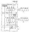
- Fig.10 is a schematic for explaining an example of a cache replace operation with BackEviction. Same reference numbers have been provided to parts that have same or similar configuration or perform same or similar functions as those shown in Fig. 9.
- Fig. 10 it is assumed that the cache memory 11 of the processor 10 is controlled by a 4-Way, W0 to W3, set associative scheme and, that all the four Ways of a certain cache index are in valid state, and that data A to D are stored in the four Ways, respectively.
- the processor 10 requests data E of the same cache index as that of data A to D from the main memory 40 (step S1401).
- the processor 10 refers to the cache memory 11 to determine a position where the data E is stored in the cache. Since all the four Ways are valid, the processor 10 determines that any one of the Ways must be made invalid. Assumed that the processor 10 selects W2 as a block to be made invalid (step S1402). The memory control device 100 is not informed that the processor 10 has selected W2 as a block to be made invalid.
- the memory control device 100 receives the request for the data E from the main memory 40 and refers to the TAG-RAM 130 to determine a position where address information of the data E is stored in the cache. Since all the Ways of the same cache index are valid, it is determined that any one Way must be made invalid. Assumed that W1 in which address information of the data B is stored is determined to be made invalid (step S1403).
- the memory control device 100 requests the processor 10 to perform a cache excluding process for the Way in which the data B is stored (step S1404).
- the processor 10 performs a cache excluding process for W1 in which the data B is stored to thereby invalidate W1 (step S1405).
- the main memory 40 sends the data E to the memory control device 100.
- the memory control device 100 receives the data E and stores address information of the data E in W1 of the TAG-RAM 130 and also sends the data E to the processor 10.
- the processor 10 receives the data E and stores the data E in W2. This completes the cache replace operation.
- the first exceptional case is a case in which data of the same line is requested from another processor before completion of BackEviction.
- BackEviction although the latest data is present in the cache memory 11, there is a time period during which the block of the corresponding data of the TAG-RAM 130 is invalidated. If the same line as that of the data is requested from another processor during this period, the data is undesirably acquired from the main memory 40 so that old data, not the latest data, is acquired.
- the second exceptional case is a case in which a line to be subjected to BackEviction is invalidated by autonomous move-out.
- a processor may autonomously exclude old data from a cache memory for the purpose of efficiently using the cache.
- the latest data on the main memory 40 can be overwritten with the old data.
- Fig. 11 is a schematic for explaining an example of an operation performed when data of the same line is requested to be acquired from another processor before completion of BackEviction. It is assumed that all the four Ways of a certain cache index are in a valid state in the cache memory 11 of the processor 10, and that data A to D are stored in the four Ways, respectively.
- the processor 10 requests the data E of the same cache index as that of the data A to D from the main memory 40 (step S1501).
- the processor 10 refers to the cache memory 11 to determine a position where the data E is stored in the cache. Since all the four Ways are valid, it is determined that any one Way must be made invalid. Assumed that W2 is selected as a block to be made invalid (step S1502).
- the memory control device 100 upon detecting that the processor 10 has requested the data E from the main memory 40, refers to the TAG-RAM 130 to determine a position where the data E is stored. Since all the four Ways of the same cache index are valid, it is determined that any one Way must be made invalid. In this case, it is determined that W1 in which address information of the data B is stored is to be made invalid (step S1503).
- the memory control device 100 requests the processor 10 to perform a cache excluding process for the Way in which the data B is stored (step S1504). At this time, W1 of the TAG-RAM 130 is invalid. The latest data of the data B is present on the cache memory 11, and the cache excluding process is not yet over. Therefore, the old data that is not updated is stored in the main memory 40.
- the processor 20 requests the data B from the main memory 40 at this timing (step S1505). Since the block in which the data B of the TAG-RAM 130 is invalid, the data requested by the processor 20 is not hit in the TAG-RAM 130 so that it is determined that the data B is not present in the caches of all the processors. The data B acquired from the main memory 40 is acknowledged by the processor 20 (step S1506). Since the data is not the latest data B, inconsistency between the data occurs.
- Fig. 12 is a schematic for explaining an example of an operation performed when a line subjected to BackEviction is invalidated by autonomous move-out. It is assumed that all the four Ways of a certain cache index are in a valid state, and that the data A to D are stored in the four Ways, respectively.
- the processor 10 requests the data E of the same cache index as that of the data A to D from the main memory 40 (step S1601).
- the processor 10 refers to the cache memory 11 to determine a position where the data E is stored in the cache. Since all the four Ways are valid, it is determined that any one Way must be made invalid. In this case, it is determined that W2 is selected as a block to be made invalid (step S1602).
- the memory control device 100 upon detecting that the processor 10 has requested the data E from the main memory 40, refers to the TAG-RAM 130 to determine a position where the address information of the data E is stored. Since all the four Ways of the same cache index are valid, it is determined that any one Way must be made invalid. In this case, it is determined that W1 in which address information of the data B is stored is determined to be made invalid (step S1603).
- step S1604 assumed that the processor 10 autonomously moves out the block in which the data B is stored.
- W1 of the cache memory 11 in which the data B is stored is invalidated due to the move-out, so that the latest data B is stored in the main memory 40.
- step S1605 a cache excluding process request, which is performed to the processor 10 by the memory control device 100, of the Way in which the data B is stored is executed.
- step S1606 if the cache excluding process is executed to write the contents in W1 of the cache memory 11 in the main memory 40 (step S1606), the data B in the main memory 40 is overwritten with data which is not latest, and inconsistency between the data occurs.
- the memory control scheme based on BackEviction may fail in the above-mentioned exceptional cases.
- a memory control scheme that does not fail even in the above-mentioned exceptional cases will be described below.
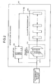
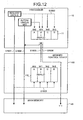
- Fig. 1 is a functional block diagram of a memory control device 100 according to an embodiment of the present invention.
- the memory control device 100 communicates with, a plurality of processors, three processors 10 to 30 in Fig. 1, and the main memory 40.
- the processors 10 to 30 are operational devices that perform various arithmetic operations.
- the processor 10 includes the cache memory 11, the processor 20 includes the cache memory 21, and the processor 10 includes the cache memory 31. It is assumed that these cache memories are managed by a 4-Way set associative scheme. Although three processors are shown in Fig. 1, the number is not limited to three.
- the main memory 40 is a storage device that temporarily stores data or computer programs that are used by the processors 10, 20, and 30.
- the memory control device 100 inputs and outputs data between the main memory 40 and the cache memories 11, 21, and 31 according to requests from the processors 10, 20, and 30 and controls the storage devices not to cause inconsistency between data in the storage devices.
- the memory control device 100 includes a request accepting unit 110, a request processing unit 120, the TAG-RAM 130, a cache control unit 140, an EWB (Early Write Back) buffer 150, an ELA (Eviction Lock Address) register 160, a re-execution deciding unit 170, and a cancel deciding unit 180.
- the EWB buffer 150 and the ELA register 160 correspond to an autonomous-exclusion-target data storing unit and an exclusion-target data storing unit, respectively.
- the request accepting unit 110 is a receiving unit that accepts data input/output requests from the processors 10 to 30, and includes a plurality of ports. These ports monitor a processing status in the request processing unit 120 until the accepted data input/output requests are completed.
- the request processing unit 120 processes a request accepted by the request accepting unit 110, and is pipelined to perform parallel processing of a plurality of requests.
- the TAG-RAM 130 is a storing unit that stores address information of data stored in the cache memories 11, 21, and 31.
- the cache control unit 140 compares address information of data requested to be input or output by the processors 10 to 30 with address information stored in the TAG-RAM 130 to determine an input/output destination or an input/output procedure of the data, updating contents of the cache memories 11, 21, and 31 and the TAG-RAM 130, and the like.
- the EWB buffer 150 stores address information of data requested to be autonomously moved out by the processors 10, 20, and 30.
- the EWB buffer 150 stores the address information at the start of autonomous move-out and holds the address information until the autonomous move-out is completed.
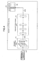
- Fig. 2 is schematic for explaining a registering/releasing operation of the EWB buffer 150.
- the requests are accepted by the request accepting unit 110, and address information of the data to be requested is stored in the EWB buffer 150 (step S101).
- the address information of the data to be requested is deleted from the EWB buffer 150 (step S102).
- the ELA register 160 stores address information of data that is being subjected to a cache excluding process by BackEviction.
- the address information to be processed is entry-registered at the start of the cache excluding process by BackEviction, and the entry is invalidated upon completion of the cache excluding process.
- Fig. 3 is a schematic for explaining a registering operation of the ELA register 160.
- the cache control unit 140 searches the TAG-RAM 130 to check whether the requested data is cached in the cache memory 11, 21, or 31 and whether all the four Ways of a cache of the same index as that of the requested data are valid. In this case, the cache control unit 140 informs the request processing unit 120 that the requested data should be acquired from the main memory 40 and that a cache excluding process should be executed to secure a place where the acquired data is stored on the cache (step S203).
- the request processing unit 120 receives the notice, transmits a data acquiring request to the main memory 40, and performs a cache excluding process request of data in the Way selected by the cache control unit 140 as a target subjected to a cache excluding process to a processor that requests the data. At this time, address information of the data stored in the Way selected as a target subjected to the cache excluding process is entry-registered in the ELA register 160 (step S204).
- each entry in the ELA register 160 has an area for storing a physical address and a valid bit (V bit) representing the validity of the entry.
- V bit a valid bit representing the validity of the entry.
- Fig. 4 is a schematic for explaining a releasing operation of the ELA register 160.
- the request finds out an entry that stores an address of data subjected to a cache excluding process in the ELA register 160 and turns the valid bit of the entry (step S303).
- the re-execution deciding unit 170 checks whether data requested with reference to the ELA register 160 is being processed by BackEviction when a memory acquiring request is made by a processor. When the data is being processed, the processing unit designates the request accepting unit 110 to re-execute the request.
- Fig. 5 is a schematic for explaining an operation of the re-execution deciding unit 170.
- data requested by a processor is being processed by BackEviction. Therefore, it is assumed that a block of the data in the TAG-RAM 130 is invalidated, and that the latest data in the cache memory of the processor is not written in the main memory 40. It is assumed that address information of the data is validly registered in the ELA register 160 by the operation in Fig. 3.
- step S401 when a memory acquiring request is made by any one of the processors 10, 20, and 30 (step S401), the request acquires any one of the ports of the request accepting unit 110. Thereafter, the request is put in the pipeline of the request processing unit 120 at a valid timing (step S402). Since the data is not hit in the TAG-RAM 130, the request processing unit 120 issues a data acquiring request to the main memory 40.
- the re-execution deciding unit 170 searches the ELA register 160 to detect whether a valid entry having the same address as that of the requested data is present, and designates the request processing unit 120 to re-execute the processing (step S403).
- the memory acquiring request is returned to the request accepting unit 110 and put in the pipeline of the request processing unit 120 again (step S404).
- the operation performed by the re-execution deciding unit 170 at step S403 is repeated until BackEviction is completed to release the entry in the ELA register 160.
- an address of data that is being subjected to BackEviction is held in the ELA register 160, and the re-execution deciding unit 170 continuously designates data acquisition from the main memory to be re-executed while a valid entry having the same address as that of data requested to be acquired by a processor is present in the ELA register 160.
- the re-execution deciding unit 170 continuously designates data acquisition from the main memory to be re-executed while a valid entry having the same address as that of data requested to be acquired by a processor is present in the ELA register 160.
- the cancel deciding unit 180 checks whether data subjected to a cache excluding process is being excluded by autonomous move-out with reference to the EWB buffer 150 when a cache excluding process performed by BackEviction is requested by a processor. When the data is being excluded by the autonomous move-out process, the cache excluding process performed by BackEviction is stopped.
- Fig. 6 is a schematic for explaining an operation of the cancel deciding unit 180.
- a memory acquiring request is made by any one of the processor 10, 20, and 30 (step S501)
- the request acquires any one of the ports of the request accepting unit 110.
- the request is put in the pipeline of the request processing unit 120 at a valid timing (step S502).
- the cache control unit 140 refers to the TAG-RAM 130
- the cache control unit 140 determines that BackEviction is necessary. It is assumed that the request processing unit 120 registers the address of the data subjected to BackEviction in the ELA register 160 and requests the processor to perform a cache excluding process.
- the cancel deciding unit 180 searches all the entries of the EWB buffer 150 to check whether an entry having the same address as that of data registered in the ELA register 160 is present. When the entry having the same address is present, the cancel deciding unit 180 turns off the valid bit of the entry in the ELA register 160 to cancel the request of the cache excluding process (step S503).
- Fig. 7 is a schematic for explaining the operation performed by the memory control device 100 when data of the same line is requested from another processor before completion of BackEviction.
- Fig. 7 relates to the first exceptional case explained in connection with Fig. 11.
- the processor 10 requests data E of the same cache index as that of data A to D from the main memory 40 (step S1101).
- the processor 10 refers to the cache memory 11 to determine a position where the data E is stored in the cache. Since all the four Ways are valid, it is determined that any one Way must be made invalid. In this case, it is assumed that W2 is selected as a block to be invalidated (step S1102).
- the memory control device 100 upon detecting that the processor 10 has requested the data E from the main memory 40, refers to a TAG-RAM 130 to determine a position where address information of the data E is stored. Since all the four Ways are valid, it is determined that any one Way, must be made invalid. In this case, it is assumed that W1 in which address information of the data B is stored is determined to be invalidated (step S1103).
- the memory control device 100 registers the address information of the data B subjected to a cache excluding process in the ELA register 160 (step S1104) and requests the processor 10 to perform a cache excluding process for the Way in which the data B is stored (step S1105).
- W1 of the TAG-RAM 130 is invalidated.
- the latest data of the data B is present on the cache memory 11, and the cache excluding process is not completed. Therefore, the old data, which is not updated, is stored in the main memory 40.
- step S1106 It is assumed that the processor 20 requests the data B from the main memory 40 at this timing (step S1106). Since the block in which the data B of the TAG-RAM 130 is invalidated, the data B requested by the processor 20 is not hit in the TAG-RAM 130. Therefore, the request processing unit 120 tries to acquire the data B from the main memory 40. However, the re-execution deciding unit 170, upon detecting that the address information of the data B being present in a valid entry in the ELA register 160, instructs the request processing unit 120 to re-execute the processing (step S1107). This re-execution of the processing is repeated while the valid entry that stores the address information of the data B is present.
- step S1105 Upon completion of the cache excluding process requested in step S1105, the latest data of the data B on the cache memory 11 is written in the main memory 40, and the corresponding entry in the ELA register 160 is invalidated (step S1108).
- the entry in the ELA register 160 is invalidated, so that the re-execution of the processing is not requested by the re-execution deciding unit.
- the main memory 40 is requested to acquire the data B (step S1109), and the data B is transmitted to the processor 20.
- the data B transmitted here is the latest data written by the cache memory 11 of a processor 10, inconsistency between the data does not occur.
- the memory control scheme according to the embodiment can maintain the consistency of the data even in the first exceptional case.
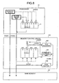
- Fig. 8 is a schematic for explaining an example of an operation performed when a line subjected to BackEviction is invalidated by autonomous move-out.
- Fig. 8 relates to the second exceptional case that is explained with reference to Fig. 12.
- the processor 10 requests data E of the same cache index as that of data A to D from the main memory 40 (step S1201).
- the processor 10 refers to the cache memory 11 to determine a position where the data E is stored in the cache. Since all the four Ways are valid, it is determined that any one Way must be made invalid. In this case, it is assumed that W2 is selected as a block to be invalidated (step S1202).
- the memory control device 100 upon detecting that the processor 10 has requested the data E from the main memory 40, refers to the TAG-RAM 130 to determine a position where address information of the data E is stored. Since all the four Ways are valid, it is determined that any one Way must be made invalid. In this case, it is assumed that W1 in which address information of the data B is stored is determined to be invalidated (step S1203).
- the request processing unit 120 invalidates W1 and registers the address information of the data B stored in W1 in the ELA register 160.
- the request processing unit 120 tries to request the processor 10 to perform a cache excluding process for the block in which the data B is stored (step S1204).
- the processor 10 autonomously moves out the block in which the data B is stored.
- W1 of the cache memory 11 in which the data B is stored is invalidated by the move-out, so that the latest data B is stored in the main memory 40.
- the address information of the data B is held in the EWB buffer 150 (step S1205).
- the cancel deciding unit 180 detects that the address information of the data B to be requested to be subjected to a cache excluding process is present in the entry in the EWB buffer 150 (step S1206).
- the cancel deciding unit 180 cancels the cache excluding process request of the block in which the data B for the processor 10 and releases the entry in the ELA register 160 (step S1207).
- the memory control scheme according to the embodiment can maintain the consistency of the data even in the first exceptional case.
- the address information of the target data is stored in the ELA register 160 at the start of a cache excluding process performed by BackEviction. While an address of data requested to be acquired by a processor is present in the ELA register 160, the request processing unit continuously re-executes the data acquiring process. Therefore, even though data of the same line is requested by another processor before completion of Backeviction, inappropriate data is not acquired.
- the address information of the target information is stored in the EWB buffer 150 at the start of autonomous move-out performed by a processor.
- a cache excluding process performed by BackEviction is stopped. Therefore, even though a line subjected to BackEviction is invalidated by autonomous move-out, inappropriate data is not overwritten in the main memory 40.
- consistency of data in the cache memories can be maintained even if processors that do not inform the memory control device of information related to the cache excluding process are used. Moreover, latency can be suppressed, the structure can be made simple.
Landscapes
- Engineering & Computer Science (AREA)
- Theoretical Computer Science (AREA)
- Physics & Mathematics (AREA)
- General Engineering & Computer Science (AREA)
- General Physics & Mathematics (AREA)
- Memory System Of A Hierarchy Structure (AREA)
Applications Claiming Priority (1)
| Application Number | Priority Date | Filing Date | Title |
|---|---|---|---|
| JP2004342802A JP2006155080A (ja) | 2004-11-26 | 2004-11-26 | メモリ制御装置およびメモリ制御方法 |
Publications (2)
| Publication Number | Publication Date |
|---|---|
| EP1662401A2 true EP1662401A2 (de) | 2006-05-31 |
| EP1662401A3 EP1662401A3 (de) | 2009-01-21 |
Family
ID=36036104
Family Applications (1)
| Application Number | Title | Priority Date | Filing Date |
|---|---|---|---|
| EP05251174A Withdrawn EP1662401A3 (de) | 2004-11-26 | 2005-02-28 | Speichersteuervorrichtung und -verfahren |
Country Status (5)
| Country | Link |
|---|---|
| US (2) | US20060117140A1 (de) |
| EP (1) | EP1662401A3 (de) |
| JP (1) | JP2006155080A (de) |
| KR (1) | KR100706852B1 (de) |
| CN (1) | CN100357917C (de) |
Families Citing this family (5)
| Publication number | Priority date | Publication date | Assignee | Title |
|---|---|---|---|---|
| JP5011885B2 (ja) * | 2006-08-18 | 2012-08-29 | 富士通株式会社 | スヌープタグの制御装置 |
| WO2008095025A1 (en) * | 2007-01-31 | 2008-08-07 | Qualcomm Incorporated | Apparatus and methods to reduce castouts in a multi-level cache hierarchy |
| CN102103549A (zh) * | 2009-12-18 | 2011-06-22 | 上海华虹集成电路有限责任公司 | 一种缓存替换方法 |
| US20160316450A1 (en) * | 2015-04-22 | 2016-10-27 | Pebble Technology Corp. | Living notifications |
| DE112016002356B4 (de) * | 2015-05-27 | 2024-02-29 | Google Inc. | Datenspeichersystemarchitektur |
Citations (2)
| Publication number | Priority date | Publication date | Assignee | Title |
|---|---|---|---|---|
| US20020199063A1 (en) * | 2001-06-26 | 2002-12-26 | Shailender Chaudhry | Method and apparatus for facilitating speculative stores in a multiprocessor system |
| US20040143709A1 (en) * | 2003-01-16 | 2004-07-22 | Ip-First, Llc. | Apparatus and method for invalidation of redundant branch target address cache entries |
Family Cites Families (10)
| Publication number | Priority date | Publication date | Assignee | Title |
|---|---|---|---|---|
| US4503497A (en) * | 1982-05-27 | 1985-03-05 | International Business Machines Corporation | System for independent cache-to-cache transfer |
| US5269009A (en) * | 1990-09-04 | 1993-12-07 | International Business Machines Corporation | Processor system with improved memory transfer means |
| US5692151A (en) * | 1994-11-14 | 1997-11-25 | International Business Machines Corporation | High performance/low cost access hazard detection in pipelined cache controller using comparators with a width shorter than and independent of total width of memory address |
| US6145059A (en) * | 1998-02-17 | 2000-11-07 | International Business Machines Corporation | Cache coherency protocols with posted operations and tagged coherency states |
| US6393540B1 (en) * | 1998-06-30 | 2002-05-21 | Emc Corporation | Moving a logical object from a set of source locations to a set of destination locations using a single command |
| WO2001063240A2 (en) * | 2000-02-25 | 2001-08-30 | Sun Microsystems, Inc. | Maintaining high snoop traffic throughput and preventing cache data eviction during an atomic operation |
| US6347360B1 (en) * | 2000-02-25 | 2002-02-12 | Sun Microsystems, Inc. | Apparatus and method for preventing cache data eviction during an atomic operation |
| US6813522B1 (en) * | 2000-12-29 | 2004-11-02 | Emc Corporation | Method of sharing memory in a multi-processor system including a cloning of code and data |
| US6925536B2 (en) * | 2002-11-05 | 2005-08-02 | Newisys, Inc. | Cache coherence directory eviction mechanisms for unmodified copies of memory lines in multiprocessor systems |
| US6892283B2 (en) * | 2002-12-05 | 2005-05-10 | International Business Machines Corporation | High speed memory cloner with extended cache coherency protocols and responses |
-
2004
- 2004-11-26 JP JP2004342802A patent/JP2006155080A/ja not_active Withdrawn
-
2005
- 2005-02-28 EP EP05251174A patent/EP1662401A3/de not_active Withdrawn
- 2005-02-28 US US11/066,760 patent/US20060117140A1/en not_active Abandoned
- 2005-03-02 KR KR1020050017115A patent/KR100706852B1/ko not_active Expired - Fee Related
- 2005-03-17 CN CNB2005100554111A patent/CN100357917C/zh not_active Expired - Fee Related
-
2010
- 2010-11-15 US US12/926,390 patent/US20110072216A1/en not_active Abandoned
Patent Citations (2)
| Publication number | Priority date | Publication date | Assignee | Title |
|---|---|---|---|---|
| US20020199063A1 (en) * | 2001-06-26 | 2002-12-26 | Shailender Chaudhry | Method and apparatus for facilitating speculative stores in a multiprocessor system |
| US20040143709A1 (en) * | 2003-01-16 | 2004-07-22 | Ip-First, Llc. | Apparatus and method for invalidation of redundant branch target address cache entries |
Also Published As
| Publication number | Publication date |
|---|---|
| CN1779664A (zh) | 2006-05-31 |
| JP2006155080A (ja) | 2006-06-15 |
| KR20060059149A (ko) | 2006-06-01 |
| CN100357917C (zh) | 2007-12-26 |
| KR100706852B1 (ko) | 2007-04-13 |
| EP1662401A3 (de) | 2009-01-21 |
| US20060117140A1 (en) | 2006-06-01 |
| US20110072216A1 (en) | 2011-03-24 |
Similar Documents
| Publication | Publication Date | Title |
|---|---|---|
| US12455836B2 (en) | Victim cache that supports draining write-miss entries | |
| US8468307B2 (en) | Information processing apparatus and order guarantee method | |
| KR101639672B1 (ko) | 무한 트랜잭션 메모리 시스템 및 그 동작 방법 | |
| KR100567099B1 (ko) | L2 디렉토리를 이용한 멀티프로세서 시스템의 가-저장촉진 방법 및 장치 | |
| KR100704089B1 (ko) | L2 디렉토리를 이용한 멀티프로세서 시스템의 가-로드촉진 방법 및 장치 | |
| JP6470300B2 (ja) | データ処理のための方法及びプロセッサ | |
| EP0833248A2 (de) | Vorrichtung und Verfahren zur Speicherung der Speicheraktualisierungsgeschichte | |
| US6260117B1 (en) | Method for increasing efficiency in a multi-processor system and multi-processor system with increased efficiency | |
| US20150331798A1 (en) | Managing memory transactions in a distributed shared memory system supporting caching above a point of coherency | |
| EP2891984B1 (de) | Verfahren zur Abruch einer Transaktion in einer Mehrkern-CPU | |
| US8296520B2 (en) | System and method for optimizing neighboring cache usage in a multiprocessor environment | |
| US20020144063A1 (en) | Multiprocessor cache coherence management | |
| US7024520B2 (en) | System and method enabling efficient cache line reuse in a computer system | |
| US20110072216A1 (en) | Memory control device and memory control method | |
| EP1622026B1 (de) | Cachespeicher-Steuereinheit und -Steuerverfahren | |
| JP2020003959A (ja) | 情報処理装置、演算処理装置及び情報処理装置の制御方法 | |
| US20080313409A1 (en) | Separating device and separating method | |
| JPH0415494B2 (de) | ||
| JP5625536B2 (ja) | キャッシュ装置、及び情報処理装置 | |
| US11016902B2 (en) | Generating recovery data for an initial state of status data for a data handling transaction and predicting a revised state of the status data applicable to resolution of the data handling transaction | |
| JPH08263374A (ja) | キャッシュ制御方法およびそれを用いたマルチプロセッサシステム | |
| JPH05342099A (ja) | バッファ記憶制御方式 | |
| GR20170200061U (el) | Μια διαταξη για τη μεταφορα δεδομενων μεταξυ περιοχων διεθυνσεων στη μνημη | |
| JPH0895860A (ja) | バッファメモリ装置 |
Legal Events
| Date | Code | Title | Description |
|---|---|---|---|
| PUAI | Public reference made under article 153(3) epc to a published international application that has entered the european phase |
Free format text: ORIGINAL CODE: 0009012 |
|
| AK | Designated contracting states |
Kind code of ref document: A2 Designated state(s): AT BE BG CH CY CZ DE DK EE ES FI FR GB GR HU IE IS IT LI LT LU MC NL PL PT RO SE SI SK TR |
|
| AX | Request for extension of the european patent |
Extension state: AL BA HR LV MK YU |
|
| PUAL | Search report despatched |
Free format text: ORIGINAL CODE: 0009013 |
|
| AK | Designated contracting states |
Kind code of ref document: A3 Designated state(s): AT BE BG CH CY CZ DE DK EE ES FI FR GB GR HU IE IS IT LI LT LU MC NL PL PT RO SE SI SK TR |
|
| AX | Request for extension of the european patent |
Extension state: AL BA HR LV MK YU |
|
| 17P | Request for examination filed |
Effective date: 20090715 |
|
| AKX | Designation fees paid |
Designated state(s): DE FR GB |
|
| 17Q | First examination report despatched |
Effective date: 20090918 |
|
| STAA | Information on the status of an ep patent application or granted ep patent |
Free format text: STATUS: THE APPLICATION IS DEEMED TO BE WITHDRAWN |
|
| 18D | Application deemed to be withdrawn |
Effective date: 20120228 |