EP1661219B1 - Semiconductor laser and method of manufacture - Google Patents
Semiconductor laser and method of manufacture Download PDFInfo
- Publication number
- EP1661219B1 EP1661219B1 EP04744842A EP04744842A EP1661219B1 EP 1661219 B1 EP1661219 B1 EP 1661219B1 EP 04744842 A EP04744842 A EP 04744842A EP 04744842 A EP04744842 A EP 04744842A EP 1661219 B1 EP1661219 B1 EP 1661219B1
- Authority
- EP
- European Patent Office
- Prior art keywords
- laser
- slot
- perturbation
- optical path
- interfaces
- Prior art date
- Legal status (The legal status is an assumption and is not a legal conclusion. Google has not performed a legal analysis and makes no representation as to the accuracy of the status listed.)
- Expired - Lifetime
Links
- 238000000034 method Methods 0.000 title claims description 26
- 238000004519 manufacturing process Methods 0.000 title claims description 11
- 239000004065 semiconductor Substances 0.000 title claims description 9
- 230000003287 optical effect Effects 0.000 claims abstract description 70
- 230000003595 spectral effect Effects 0.000 claims description 29
- 239000000463 material Substances 0.000 claims description 21
- 238000005530 etching Methods 0.000 claims description 11
- 238000007373 indentation Methods 0.000 claims description 11
- 230000001965 increasing effect Effects 0.000 claims description 4
- 238000001228 spectrum Methods 0.000 description 31
- 238000013461 design Methods 0.000 description 11
- 230000000694 effects Effects 0.000 description 9
- 239000011248 coating agent Substances 0.000 description 8
- 238000000576 coating method Methods 0.000 description 8
- 230000008569 process Effects 0.000 description 8
- 238000002310 reflectometry Methods 0.000 description 6
- 238000012545 processing Methods 0.000 description 5
- 230000008859 change Effects 0.000 description 4
- 238000005253 cladding Methods 0.000 description 4
- 238000013459 approach Methods 0.000 description 3
- 230000001419 dependent effect Effects 0.000 description 3
- 239000013078 crystal Substances 0.000 description 2
- 230000001066 destructive effect Effects 0.000 description 2
- 239000002184 metal Substances 0.000 description 2
- 238000000926 separation method Methods 0.000 description 2
- 235000008694 Humulus lupulus Nutrition 0.000 description 1
- 230000008901 benefit Effects 0.000 description 1
- 230000015572 biosynthetic process Effects 0.000 description 1
- 238000004364 calculation method Methods 0.000 description 1
- 239000000470 constituent Substances 0.000 description 1
- 239000007799 cork Substances 0.000 description 1
- 230000008021 deposition Effects 0.000 description 1
- 238000007865 diluting Methods 0.000 description 1
- 238000009826 distribution Methods 0.000 description 1
- 239000002019 doping agent Substances 0.000 description 1
- 238000000295 emission spectrum Methods 0.000 description 1
- 230000002708 enhancing effect Effects 0.000 description 1
- 238000002474 experimental method Methods 0.000 description 1
- 230000006872 improvement Effects 0.000 description 1
- 238000005468 ion implantation Methods 0.000 description 1
- 230000007246 mechanism Effects 0.000 description 1
- 230000003534 oscillatory effect Effects 0.000 description 1
- 230000001151 other effect Effects 0.000 description 1
- 238000000206 photolithography Methods 0.000 description 1
- 238000004088 simulation Methods 0.000 description 1
- 239000007787 solid Substances 0.000 description 1
- 239000000758 substrate Substances 0.000 description 1
Images









Classifications
-
- H—ELECTRICITY
- H01—ELECTRIC ELEMENTS
- H01S—DEVICES USING THE PROCESS OF LIGHT AMPLIFICATION BY STIMULATED EMISSION OF RADIATION [LASER] TO AMPLIFY OR GENERATE LIGHT; DEVICES USING STIMULATED EMISSION OF ELECTROMAGNETIC RADIATION IN WAVE RANGES OTHER THAN OPTICAL
- H01S5/00—Semiconductor lasers
- H01S5/06—Arrangements for controlling the laser output parameters, e.g. by operating on the active medium
- H01S5/065—Mode locking; Mode suppression; Mode selection ; Self pulsating
-
- H—ELECTRICITY
- H01—ELECTRIC ELEMENTS
- H01S—DEVICES USING THE PROCESS OF LIGHT AMPLIFICATION BY STIMULATED EMISSION OF RADIATION [LASER] TO AMPLIFY OR GENERATE LIGHT; DEVICES USING STIMULATED EMISSION OF ELECTROMAGNETIC RADIATION IN WAVE RANGES OTHER THAN OPTICAL
- H01S5/00—Semiconductor lasers
- H01S5/10—Construction or shape of the optical resonator, e.g. extended or external cavity, coupled cavities, bent-guide, varying width, thickness or composition of the active region
- H01S5/1021—Coupled cavities
-
- H—ELECTRICITY
- H01—ELECTRIC ELEMENTS
- H01S—DEVICES USING THE PROCESS OF LIGHT AMPLIFICATION BY STIMULATED EMISSION OF RADIATION [LASER] TO AMPLIFY OR GENERATE LIGHT; DEVICES USING STIMULATED EMISSION OF ELECTROMAGNETIC RADIATION IN WAVE RANGES OTHER THAN OPTICAL
- H01S5/00—Semiconductor lasers
- H01S5/20—Structure or shape of the semiconductor body to guide the optical wave ; Confining structures perpendicular to the optical axis, e.g. index or gain guiding, stripe geometry, broad area lasers, gain tailoring, transverse or lateral reflectors, special cladding structures, MQW barrier reflection layers
- H01S5/22—Structure or shape of the semiconductor body to guide the optical wave ; Confining structures perpendicular to the optical axis, e.g. index or gain guiding, stripe geometry, broad area lasers, gain tailoring, transverse or lateral reflectors, special cladding structures, MQW barrier reflection layers having a ridge or stripe structure
- H01S5/223—Buried stripe structure
- H01S5/2231—Buried stripe structure with inner confining structure only between the active layer and the upper electrode
-
- H—ELECTRICITY
- H01—ELECTRIC ELEMENTS
- H01S—DEVICES USING THE PROCESS OF LIGHT AMPLIFICATION BY STIMULATED EMISSION OF RADIATION [LASER] TO AMPLIFY OR GENERATE LIGHT; DEVICES USING STIMULATED EMISSION OF ELECTROMAGNETIC RADIATION IN WAVE RANGES OTHER THAN OPTICAL
- H01S5/00—Semiconductor lasers
- H01S5/06—Arrangements for controlling the laser output parameters, e.g. by operating on the active medium
- H01S5/065—Mode locking; Mode suppression; Mode selection ; Self pulsating
- H01S5/0656—Seeding, i.e. an additional light input is provided for controlling the laser modes, for example by back-reflecting light from an external optical component
-
- H—ELECTRICITY
- H01—ELECTRIC ELEMENTS
- H01S—DEVICES USING THE PROCESS OF LIGHT AMPLIFICATION BY STIMULATED EMISSION OF RADIATION [LASER] TO AMPLIFY OR GENERATE LIGHT; DEVICES USING STIMULATED EMISSION OF ELECTROMAGNETIC RADIATION IN WAVE RANGES OTHER THAN OPTICAL
- H01S5/00—Semiconductor lasers
- H01S5/10—Construction or shape of the optical resonator, e.g. extended or external cavity, coupled cavities, bent-guide, varying width, thickness or composition of the active region
- H01S5/1003—Waveguide having a modified shape along the axis, e.g. branched, curved, tapered, voids
- H01S5/1017—Waveguide having a void for insertion of materials to change optical properties
Definitions
- the present invention relates a semiconductor laser, in particular such a laser which operates with substantially single longitudinal mode emission.
- the perturbations may be caused by any index altering means which modifies the refractive index profile of the waveguide to an appropriate degree to manipulate optical feedback and hence the spectral content of the device. While the description of the present invention which follows refers primarily to the case where the perturbations are defined by slots etched along the device it will be appreciated by a person skilled in the art that the teaching of the invention is equally applicable to other forms of perturbations (for example modifying the refractive index profile by employing doping or ion implantation methods).
- 'slot length' refers to the distance between the longitudinal slot faces in the device material, ie 'slot length' is measured along the direction of light propagation, d.
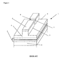
- Figures 1 and 2 illustrate a typical prior art slotted laser 1 having a single rectangular slot 6.
- a device comprises waveguiding layers 2 (containing for example a multiple quantum well structure) covered by an upper cladding layer 4.
- Primary optical feedback means are provided in the form of a cleaved facet 8 at either end of the device. The distance between the facets determines the exact wavelengh's of the Fabry Perot modes of the cavity.
- the upper cladding layer 4 forms a ridge 3 having a cap layer 5.
- the slot features in such known devices are formed by etching a rectangular slot 6 in the ridge waveguide 3, resulting in two longitudinal interfaces 7 that are perpendicular to the direction of light propagation, d, within the device.
- ⁇ is the free spectral range
- ⁇ is the free space wavelength of the light
- n eff is the effective index of the optical mode in the laser cavity.
- L is again the cavity length of the laser and N is an integer.
- the present invention provides a semiconductor single longitudinal mode laser according to claim 1, a method of manufacturing a semiconductor laser according to claim 13 and a method of increasing the free spectral range of a semiconductor laser device according to claim 19.
- the laser comprises a ridge and at least one effective refractive index perturbation is formed by a slot defined in the ridge.
- each perturbation comprises a slot formed along the ridge.
- the contributing interface of each perturbation is substantially planar and substantially perpendicular to the longitudinally extending optical path.
- At least one slot comprises a first face which is substantially planar and substantially perpendicular to the longitudinally extending optical path and a second face which is non-perpendicular to the optical path and is preferably substantially stepped, curved or angled with respect to the first face.
- Such slot design minimises or prevents destructive interference between interfaces.
- the interfaces which are substantially perpendicular to the optical path contribute to optical feedback within the device, with feedback from non-perpendicular interfaces being suppressed thus improving performance characteristics of the laser.
- a laser comprising a ridge has at least one effective refractive index perturbation is formed by one or more indentations defined in the side of the ridge.
- each perturbation may be formed by indentations defined in the ridge.
- a series of effective refractive index perturbations may be employed wherein the spacing between adjacent contributing interfaces is a uniform number of quarter or half material wavelengths.
- One or more additional series of effective refractive index perturbations may be overlaid with a first series of perturbations. Such series of perturbations result in devices with a larger effective free spectral range.
- two or more slots are of different length (while the spacing between adjacent contributing faces is a uniform number of half wavelengths).
- the effect of such 'chirped' slots is that the contributing faces can result in constructive interference of the optical feedback within the cavity whereas the non-contributing faces do not since the lengths of individual slots are different from each other.
- the present invention also relates to a method of manufacturing a laser comprising the steps of: (1) forming a laser cavity with a lasing medium, the laser cavity defining a longitudinally extending optical path and having a facet at either end, and (2) forming optical feedback means by introducing a plurality of perturbations into the laser cavity, each perturbation defining two longitudinal interfaces; characterised in that , the longitudinal interfaces of at least one perturbation are adapted such that only one interface contributes to optical feedback along the longitudinally extending optical path. That is to say that, for at least one perturbation, only one interface contributes to optical feedback along the longitudinally extending optical path.
- the cavity is formed with a longitudinally extending ridge and at least one perturbation is provided by etching a slot in the ridge.
- At least one slot is formed with a first face which is substantially planar and substantially perpendicular to the longitudinally extending optical path and a second face which is non-perpendicular to the optical path and is preferably substantially curved, stepped or angled with respect to the first face.
- perturbations may be provided by etching one or more indentations in the side of the ridge.
- the method of the invention improves processing tolerances and enhances temperature characteristics of the resultant laser as shall be described further below.
- the invention also provides a method of increasing the free spectral range of a laser device according to claim 19
- FIGS 1 and 2 show a prior art device 1 formed of waveguiding layers 2 (typically having a multiple quantum well structure), upper cladding layer 4 and cap layer 5 with a facet 8 at either end.
- a ridge 3 extends longitudinally along the top of the device 1.
- One rectangular slot feature 6 is shown etched in the ridge 3 giving rise to slot faces 7 which are substantially perpendicular to the longitudinal direction of light propagation within the device.
- Figure 3 illustrates how, as a result of offset due to process bias, the contributing interfaces 9 defined by faces 7 of rectangular slot 6 cannot be properly positioned with respect to other such contributing interfaces in the laser cavity with an accuracy high enough to ensure constructive interference at the appropriate wavelength.
- each face of the slot will contribute to the overall optical feedback.
- the present invention reduces the optical feedback provided by the interfaces on a particular side of a given number of slots to such an extent that they can be ignored. This approach thus allows greater control of the lasers spectral content.
- any change in slot length will have profound effects on the mirror loss spectrum and thus emission wavelength of the device.
- this is no longer a problem since the spectral selectivity of the slot features is now no longer dependent upon the size of the slots themselves.
- the only dimensions which remain critical are the distances between those interfaces which provide a significant amount of optical feedback. Since these dimensions are typically more than an order of magnitude greater than the length of the slots themselves the accuracy with which these features have to be positioned is also relaxed by more than an order of magnitude.
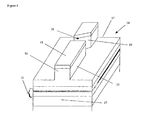
- Figures 4 and 5 show a device 10 according to the invention (having a similar structure to the device 1 in Figure 1 ) with waveguiding layers 12, upper cladding layer 14, cap layer 15, ridge 13 and facets 17.
- an angled slot feature 16 is formed having a first face 18 perpendicular to the light propagation directions and a second face 19 angled with respect to the first face 18.
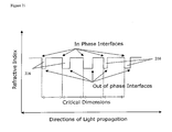
- the introduction of one or more slots (or equivalent features) causes perturbation of the lasing medium which is reflected in the change in refractive index profile (see Figure 6 ).
- Interface 20 defined by an abrupt change in effective refractive index will contribute to optical feedback along the optical path, while interface 21 will not.
- the present invention allows for lithographic tolerances to be relaxed when making single longitudinal mode devices at specified wavelengths. It also allows the emission wavelengths of adjacent laser elements in a bar format to be positioned precisely respect to each other. Moreover it allows this to clone exactly with more relaxed lithographic tolerances than could be employed in the fabrication of known slotted lasers incorporating rectangular etched features.
- the invention is based on the premise that structural features (such as slots, doped regions or the like) can be used to modify the effective refractive index profile of a device.
- the effective refractive index is obtained by summing the products of the refractive index in a particular region of the laser cavity and the fraction of the optical intensity which is present in that region, and dividing this value by the integral over the spatial extent of the optical field.
- Such structural features cause perturbation of the refractive index profile within the device, thus influencing performance characteristics.
- the faces of a slot etched in the ridge of a laser such as that shown in Figure 4 cause interfaces between regions of higher and lower refractive index - the interfaces being defined by the physical characteristics of the slot.
- the present invention enables the performance characteristics of a laser to be enhanced by employing slot designs that perturb the refractive index profile so that there is only one contributing interface associated with each slot.
- rectangular slot features employed in prior art devices have two contributing interfaces associated with each slot.
- etched features which fulfil the requirement of providing only one contributing interface, are discussed below. Also discussed below are example patterns of such features that enable single longitudinal emission at a specified wavelength over an extended temperature range. It is noted that the patterns and their constituent etched features can be used interchangeably to achieve the desired spectral content.
- each slot pattern has two distinct design elements associated with it, the first is shape of etched slot features the second is positions of these features with respect to one another and the facets of the laser cavity.
- a slot should produce a refractive index profile such as that shown in Figure 6 having a first contributing interface 20 and a second non-contributing interface 21.
- the desired refractive index effect may be produced by the introduction of an angled, sloped, stepped, curved (or combination thereof) or other suitable slot into the ridge 13.
- Figure 6 depicts slots 22 each having a conventional planar face 18 and a 'v-shaped' face 22. Any other effect upon refractive index which has the result that the second interface does not contribute substantially to optical feedback within the along the longitudinal optical path will suffice for the purposes of the invention.
- the key aspect of the present invention is therefore that the refractive index profile associated with at least one perturbation or slot is such that only one of the two longitudinal interfaces contributes to optical feedback.
- Figure 7 illustrates examples of different slot configurations, which may be used in the present invention, specifically the slot features (a) and (e) are referred to as being tapered, the features (c) and (g) are referred to as being curved, the features (d) and (f) are referred to as being corrugated, feature (b) is referred to as being angled and the feature (h) is referred to as being stepped tapered.
- the common trait being that they each have one interface which is substantially perpendicular to the direction of light propagation in the laser cavity (contributing to optical feedback), while the other side of the slot is designed to suppress optical feedback (eg by being curved or angled with respect to the first interface).
- the selection of devices shown in Figure 7 is not an attempt to provide a comprehensive set of designs instead it merely illustrates a number of possible implementations.
- each slot defines a first interface (or contributing interface) which is substantially planar and substantially perpendicular to the longitudinally extending optical path and a second interface (or feedback suppressing interface) which is substantially curved or angled with respect to the first interface.
- the contributing interface acts in the usual manner to provide optical feedback to L / N th modes while the suppressing interface is designed to avoid adding to the optical feedback within the laser cavity.
- Having the second interface curved or angled with respect to the first reduces the amount of optical feedback it can provide to any particular longitudinal mode for two reasons. Firstly, light which interacts with a curved or angled interface is more likely (than light interacting with a planar interface aligned perpendicular to its direction of propagation) to be scattered out of the laser cavity.
- Specifying the emission wavelength of a laser diode, by etching features discussed above can be achieved by placing the interfaces which provide the bulk of the optical feedback, i.e. the straight interfaces which are perpendicular to the direction of light propagation, at distances from one another that correspond to multiples of half the free space emission wavelength divided by effective refractive index of the lasing mode.
- ⁇ m which is the wavelength of light in the laser cavity, this is also known as the material wavelength.
- the problem of achieving single longitudinal mode laser emission at a specified wavelength over a particular temperature range is also addressed by the present invention. In order to do this it is necessary to discriminate against enough of the longitudinal modes of cavity to cope with changes in the laser's gain spectrum that occur over the temperature interval in question. Once the number of longitudinal modes (of the unperturbed structure) which must be discriminated against for a particular application is determined the appropriate slot pattern can be determined. For the most basic type of slot patterns, i.e.
- Figure 8 shows the calculated mirror loss spectrum of one embodiment of the invention, a device which has ten etched tapered slot features. These features are positioned along the cavity so as to produce lasing emission at 1.55 ⁇ m, as such their high feedback interfaces were separated by a distance of sixteen material wavelengths. Since lasing emission occurs at wavelengths which correspond to minima in the mirror loss spectrum it is immediately apparent that the effective free spectral range of this laser is 45nm, assuming the gain spectrum is sufficiently flat, this is the same value as that obtained using Equation 3.
- Figure 9 illustrates the positions these slot features in the laser cavity.
- the slot features themselves have an average length of 0.3 ⁇ m, their associated contributing interfaces having an effective refractive index step of 0.008, while the angled face of each slot feature consisted of eight sub-units each providing an effective index step of 0.001, and staggered along the cavity by about 10 nm (see Figure 10 ).
- the portion of the laser cavity containing the tapered slots is characterised by a series of slots etched at constant spacing of 32 half material wavelengths.
- Figure 11 is the calculated mirror loss spectrum for a device according to a second embodiment comprising a different pattern of ten tapered slot features (see Figure 13 ).
- This embodiment exhibits a greater effective free spectral range and therefore will maintain single longitudinal emission over far greater temperature ranges. Specifically the effective free spectral range is greater than 80nm, this would provide signal longitudinal mode emission over a temperature range about 160°C.
- Figure 12 shows the mirror loss spectra for three simple slot patterns analogous to that shown in Figure 9 , all designed to obtain single longitudinal mode at the same wavelength, in this specific case the wavelength in question in 1.55 ⁇ m.
- the slot pattern ( Figure 13 ) which was used to obtain the mirror loss spectra in Figure 11 can be thought of as a combination of the three patterns which were used to produce the various mirror loss spectra found in Figure 12 ie three individual series having slot separations of 29, 44 and 62 half material wavelengths. As the only wavelength at which this combination of patterns constructively interferes is the design wavelength, the result is an enhanced effective free spectral range. This approach offers an improvement over simpler slot patterns, which consist of just one fixed number of half material wavelengths between adjacent slot faces defining the contributing interfaces.
- a number of laser diode devices incorporating various configurations of tapered slot features were fabricated. These devices were fabricated using standard processing techniques. The steps used in the manufacture of the devices, whose characteristics are detailed here, were as follows.
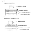
- Steps 2, 3, 4, 5 and 6 respectively are illustrated in Figure 14, (a) to (e) .
- the slot patterns which were incorporated into the fabricated devices were designed to demonstrate two principal aspects of the invention. Namely the ability to fabricate single longitudinal mode laser diodes which emit at a stipulated wavelength, and the ability to manipulate the mirror loss spectrum of a laser diode so as to allow a laser emitting in a single longitudinal to operate over a predetermined temperature range without suffering from mode hops. It is noted that the data below was obtained on prototype samples, which were fabricated at the same time, and that the samples used in this these experiments had a high reflectivity coating applied to one facet, and a low reflectivity coating applied to the other facet.
- the measured lasing wavelength turned out to be 1.577 ⁇ m (operating at a temperature 20 °C).
- the difference between the design wavelength and experimentally measured wavelength was attributed to the fact that the effective index of the guided mode was not known to a high enough accuracy at design time.
- the design of the tapered slot features, which were incorporated into the first set of devices, is shown in Figure 15 . Given that there are twenty material wavelengths between the contributing interfaces of the slot features, the effective free spectral range of the device was calculated to be 36 nm.
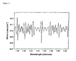
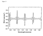
- Figure 16 shows the wavelength spectra obtained from the device at 10 °C, 20 °C, 30 °C and 85 °C. To allow interpretation of the graph it is noted the emission wavelength always increases with temperature. Mode hop free operation is demonstrated range over the temperature range 20 °C to 85 °C, by virtue of the fact that the rate at which the wavelength tuned with temperature, over this range, was measured to be 0.1 nm/°C. It is also noteworthy that the emission wavelength at 10 °C is separated by approximately 36 nm from the emission wavelength 20 °C. This shows that the effective free spectral range agrees with that predicted by theory ( Figure 17 ). The large effective free spectral ranges achieved with the present invention have not been obtained using devices incorporating conventional slot patterns.
- each device contained ten pairs of such indentations, the indentations closest to the low reflectivity coating were positioned such that their contributing interfaces were 50 ⁇ m from the crystal facet that that is adjacent to the low reflectivity coating.
- the only difference between patterns of indentations was that in first case the contributing interfaces of the slot features were designed to be spaced at twenty material wavelength appropriate to achieving emission a 1.550 ⁇ m, while in the second pattern the contributing interfaces of the slot features were designed to be separated by twenty wavelengths appropriate to achieving emission at 1.545 ⁇ m.
- the inability to specify the wavelength correctly is due to the fact that the precise value of the effective index was not known at design time.
- the wavelengths of the individual devices are both 6 nm away from their respective design wavelength's, the separation between these wavelength's is 5 nm as specified. It is also noted that since the effective index of the lasing mode may be calculated from the wavelength emission spectra, the emission wavelengths of future devices may be specified much more accurately.
- a laser according to the invention comprises a rectangular slot pattern which allows some of the manufacturing tolerances usually associated with these perturbation features to be relaxed.
- the lengths of individual slots are varied (ie the lengths of two or more slots are different from each other).
- the first face (or contributing face) of each slot is aligned (or in phase) so as to interfere constructively with light reflected from other such faces and thus contribute to optical feedback along the optical path.
- the corresponding second faces are out of phase and cause destructive interference and thus are non-contributing in terms of the optical feedback along the optical path.
- this embodiment of the invention has the advantage of facilitating greater manufacturing tolerances. From a manufacturing perspective the critical tolerances are reduced from the placement of two faces per slot (as is the case in prior art devices, as shown for example in Figures 1 to 3 ) to one face per slot as indicated in Figure 21 .
Landscapes
- Physics & Mathematics (AREA)
- Condensed Matter Physics & Semiconductors (AREA)
- General Physics & Mathematics (AREA)
- Electromagnetism (AREA)
- Optics & Photonics (AREA)
- Geometry (AREA)
- Semiconductor Lasers (AREA)
Abstract
Description
- The present invention relates a semiconductor laser, in particular such a laser which operates with substantially single longitudinal mode emission.
- Achieving single mode emission by introducing perturbations at prescribed positions along the length of a device is known, see
EP 1 214 763S82521 - In general terms, the perturbations may be caused by any index altering means which modifies the refractive index profile of the waveguide to an appropriate degree to manipulate optical feedback and hence the spectral content of the device. While the description of the present invention which follows refers primarily to the case where the perturbations are defined by slots etched along the device it will be appreciated by a person skilled in the art that the teaching of the invention is equally applicable to other forms of perturbations (for example modifying the refractive index profile by employing doping or ion implantation methods).
- The term 'slot length' (designated Lslot in
Figure 1 ) as used herein refers to the distance between the longitudinal slot faces in the device material, ie 'slot length' is measured along the direction of light propagation, d.Figures 1 and2 illustrate a typical prior art slottedlaser 1 having a singlerectangular slot 6. Typically such a device comprises waveguiding layers 2 (containing for example a multiple quantum well structure) covered by an upper cladding layer 4. Primary optical feedback means are provided in the form of a cleavedfacet 8 at either end of the device. The distance between the facets determines the exact wavelengh's of the Fabry Perot modes of the cavity. The upper cladding layer 4 forms aridge 3 having acap layer 5. The slot features in such known devices are formed by etching arectangular slot 6 in theridge waveguide 3, resulting in twolongitudinal interfaces 7 that are perpendicular to the direction of light propagation, d, within the device. - The mechanism where by slotted lasers achieve their single mode performance may be described as follows:
- It is well known that the free spectral range of a laser is given by

and as such is in effect determined by the cavity length, L, of the device. Where, Δλ, is the free spectral range, λ, is the free space wavelength of the light and, neff , is the effective index of the optical mode in the laser cavity. However it is observed that by placing reflective interfaces in the laser cavity at intervals separated L/N it is possible to discriminate against all but every N th Fabry Perot mode (ie to enhance approximately every Nth mode). Where L is again the cavity length of the laser and N is an integer. This is essentially what occurs in a slotted laser, except for the fact that when a rectangular slot feature is etched into a laser cavity, two reflective interfaces are created simultaneously. What is important to note here is that each of the reflective interfaces created provides a similar amount of optical feedback. It is also important to realise that the length of the etched slot features must be kept reasonably small (typically 3 µm). The principal reasons for this are the following: Firstly, the internal loss in the waveguide beneath slots is substantially higher that elsewhere in the cavity. Secondly, since the dopant concentration in the semiconductor material below the bottom of a slot may be less than one tenth of that in the cap layer it is impossible to create a low resistance metal contact on this material. This means that if the length of a slot feature is increased arbitrarily, then a portion of material beneath the slot will remain unpumped. - In order to accurately specify the emission wavelength of a device it is necessary to be able to position all the edges of the slot features relative to each other with an accuracy that is inversely proportional to the distance between them. This can be understood by recognising that the standing wave conditions in a long cavity device are less effected by a fixed change in the length of the cavity, Δx, than the standing wave conditions in a short cavity device. (It is noted that since the facets of a device provide a significant amount of optical feedback, the positioning of these interfaces with respect to the slot features is important). As typical slotted lasers incorporate etched features, the length's of which are less than an order of magnitude greater than the wavelength of the optical field in the laser cavity. Alto given that the two interfaces of a given conventional slot feature provide a significant amount of optical feedback, then it can be appreciated that the emission wavelengths, or more precisely the mirror loss spectra of such devices, are extremely sensitive to errors in the distance between the interfaces of such a feature. The emission wavelength of a slotted laser is thus critically dependent on length of the slot features themselves. The process of accurately realising a slot feature of a given length is therefore also important.
- The most important factor in determining the accuracy with which a slot feature can be implemented is the choice of lithographic technique used. This varies between +/- 10-20 nm for e-beam systems to +/- 100- 200 nm optical lithography systems. Beyond the accuracy of the lithographic system itself, the procedure of realising a rectangular slot feature of a certain length is also severely hampered by the bias associated with etching process (the offset due to process bias is designated Opb in
Figure 3 ). This is a problem because the length of a slot feature with parallel edges is affected by the bias of the etching process and therefore the critical dimensions in the slot pattern may be changed. As a result of these factors it is difficult, using standard lithographic and processing techniques, to sufficiently control the length of a rectangular slot feature and thus specify the spectral content of a device containing such features. - As discussed above there are considerable difficulties in accurately specifying the emission wavelength of slotted lasers. It is an object of the present invention to address these difficulties. It is a further object of the invention to provide manufacturing method, which addresses the problems, associated with processing bias and the resulting effect on slot positioning.
- It is a still further object to provide a substantially single mode laser whose performance is less temperature dependent.
- It is another object of the invention to provide a method of enhancing the free spectral range of a laser and to provide a laser having improved free spectral range.
- The present invention provides a semiconductor single longitudinal mode laser according to
claim 1, a method of manufacturing a semiconductor laser according toclaim 13 and a method of increasing the free spectral range of a semiconductor laser device according toclaim 19. - Preferably the laser comprises a ridge and at least one effective refractive index perturbation is formed by a slot defined in the ridge. In a preferred embodiment each perturbation comprises a slot formed along the ridge.
- It is preferred that the contributing interface of each perturbation is substantially planar and substantially perpendicular to the longitudinally extending optical path.
- Preferably at least one slot comprises a first face which is substantially planar and substantially perpendicular to the longitudinally extending optical path and a second face which is non-perpendicular to the optical path and is preferably substantially stepped, curved or angled with respect to the first face. Such slot design minimises or prevents destructive interference between interfaces.
- According to the invention only the interfaces which are substantially perpendicular to the optical path contribute to optical feedback within the device, with feedback from non-perpendicular interfaces being suppressed thus improving performance characteristics of the laser.
- In an alternative embodiment a laser comprising a ridge has at least one effective refractive index perturbation is formed by one or more indentations defined in the side of the ridge. Suitably each perturbation may be formed by indentations defined in the ridge.
- Typically a series of effective refractive index perturbations may be employed wherein the spacing between adjacent contributing interfaces is a uniform number of quarter or half material wavelengths. One or more additional series of effective refractive index perturbations may be overlaid with a first series of perturbations. Such series of perturbations result in devices with a larger effective free spectral range.
- In a further embodiment two or more slots are of different length (while the spacing between adjacent contributing faces is a uniform number of half wavelengths). The effect of such 'chirped' slots is that the contributing faces can result in constructive interference of the optical feedback within the cavity whereas the non-contributing faces do not since the lengths of individual slots are different from each other.
- The present invention also relates to a method of manufacturing a laser comprising the steps of: (1) forming a laser cavity with a lasing medium, the laser cavity defining a longitudinally extending optical path and having a facet at either end, and (2) forming optical feedback means by introducing a plurality of perturbations into the laser cavity, each perturbation defining two longitudinal interfaces; characterised in that, the longitudinal interfaces of at least one perturbation are adapted such that only one interface contributes to optical feedback along the longitudinally extending optical path. That is to say that, for at least one perturbation, only one interface contributes to optical feedback along the longitudinally extending optical path.
- Preferably the cavity is formed with a longitudinally extending ridge and at least one perturbation is provided by etching a slot in the ridge.
- Preferably at least one slot is formed with a first face which is substantially planar and substantially perpendicular to the longitudinally extending optical path and a second face which is non-perpendicular to the optical path and is preferably substantially curved, stepped or angled with respect to the first face. Alternatively perturbations may be provided by etching one or more indentations in the side of the ridge.
- The method of the invention improves processing tolerances and enhances temperature characteristics of the resultant laser as shall be described further below.
- The invention also provides a method of increasing the free spectral range of a laser device according to
claim 19 - The invention is described in further detail below with reference to the accompanying drawings in which:
-
Figure 1 illustrates a prior art slotted laser device comprising a single rectangular slot feature; -
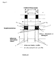
Figure 2 is a plan view of the prior art structure shown inFigure 1 ; -
Figure 3 is a schematic representation of the effects of the processing bias on the positioning of rectangular slots within a prior art device; -
Figure 4 shows a slotted laser device comprising a single angled slot; -
Figure 5 is a plan view of the device shown inFigure 4 ; -
Figure 6 illustrates the critical dimensions in a laser according to the invention incorporating angled slot features and the effect on the refractive index caused by introducing angled slots; -
Figure 7 illustrates examples of different slot configurations, which may be used in the present invention; -
Figure 8 is the calculated mirror loss spectrum for a device incorporating angled slot features separated by 32 appropriate half material wavelengths to achieve single mode emission at 1.55µm; -
Figure 9 illustrates the angled slot pattern used to obtain the calculated mirror loss spectrum shown inFigure 8 ; -
Figure 10 illustrates in more detail the slot feature used in the simulations which produced the calculated mirror profiles inFigures 8 ,11 and12 ; -
Figure 11 is a calculated mirror loss spectrum obtained using a slot pattern in which the angled features are separated by different numbers of half material wavelengths, the slot pattern in question being designed to achieve single mode emission at 1.55µm (note the very large effective free spectral range); -
Figure 12 consists of three overlaid calculated mirror loss spectra from 3 different slot patterns all designed to obtain single longitudinal mode emission at 1.55µm (the solid, dashed and dotted spectra were respectively obtained using patterns in which the angled slot features were separated by 29, 44 and 62 half material wavelengths); -
Figure 13 illustrates an angled slot pattern used in calculation of the mirror loss spectra shown inFigure 11 ; -
Figure 14 (a-e) shows side profile views of a device at various at stages in the fabrication process. -
Figure 15 illustrates aspects of the tapered slot pattern, which was used to experimentally demonstrate the utility of the present invention in fabricating laser diode devices having large effective free spectral ranges; -
Figure 16 combines the spectra of a device operating at 10°C, 20°C, 30°C and 85°C, which incorporated the slot pattern illustrated inFigure 15 ; -
Figure 17 is the calculated mirror loss spectra for the slot pattern illustrated inFigure 15 ; -
Figure 18 is the measured wavelength spectrum from a device designed to emit at 1.550µm; -
Figure 19 is the measured wavelength spectrum from device designed to emit at 1.545µm; and -
Figure 20 details the tapered slot/indentation pattern used in the devices giving rise to the spectra shown inFigures17 and18 .Figure 21 illustrates an embodiment of the invention comprising chirped slots in which the lengths of individual slots differ. - Known slotted lasers suffer from the problems discussed above. These problems stem from the fact that prior art slot patterns form pairs of contributing interfaces (or interfaces providing feedback) separated by very small distances (typically < 3µm) as illustrated in
Figure 3 .Figures 1 and2 show aprior art device 1 formed of waveguiding layers 2 (typically having a multiple quantum well structure), upper cladding layer 4 andcap layer 5 with afacet 8 at either end. Aridge 3 extends longitudinally along the top of thedevice 1. Onerectangular slot feature 6 is shown etched in theridge 3 giving rise to slot faces 7 which are substantially perpendicular to the longitudinal direction of light propagation within the device.Figure 3 illustrates how, as a result of offset due to process bias, the contributinginterfaces 9 defined byfaces 7 ofrectangular slot 6 cannot be properly positioned with respect to other such contributing interfaces in the laser cavity with an accuracy high enough to ensure constructive interference at the appropriate wavelength. Specifically, in the case of such rectangular slots, each face of the slot will contribute to the overall optical feedback. The present invention reduces the optical feedback provided by the interfaces on a particular side of a given number of slots to such an extent that they can be ignored. This approach thus allows greater control of the lasers spectral content. - Where the length of a slot is constrained by the factors outlined above, any change in slot length will have profound effects on the mirror loss spectrum and thus emission wavelength of the device. As a result of the present invention this is no longer a problem since the spectral selectivity of the slot features is now no longer dependent upon the size of the slots themselves. The only dimensions which remain critical are the distances between those interfaces which provide a significant amount of optical feedback. Since these dimensions are typically more than an order of magnitude greater than the length of the slots themselves the accuracy with which these features have to be positioned is also relaxed by more than an order of magnitude.
-
Figures 4 and5 show adevice 10 according to the invention (having a similar structure to thedevice 1 inFigure 1 ) withwaveguiding layers 12, upper cladding layer 14,cap layer 15,ridge 13 andfacets 17. In the embodiment shown anangled slot feature 16 is formed having afirst face 18 perpendicular to the light propagation directions and asecond face 19 angled with respect to thefirst face 18. The introduction of one or more slots (or equivalent features) causes perturbation of the lasing medium which is reflected in the change in refractive index profile (seeFigure 6 ).Interface 20 defined by an abrupt change in effective refractive index will contribute to optical feedback along the optical path, whileinterface 21 will not. - Considering
Figures 3 and6 and the problem of the bias associated with the etching process, it becomes apparent that with the present invention this is no longer an issue, since the length of the slot feature has now no bearing on the spectral distribution of the mirror loss spectrum of the device and thus no bearing on its emission wavelength. Moreover, if the interfaces which provide the bulk of optical feedback are all provided on same side of the slot features it is clear that process bias will effect all these interfaces in the same way, as shown inFigure 6 , thus having a reduced effect on the critical dimensions. Essentially, the present invention allows for lithographic tolerances to be relaxed when making single longitudinal mode devices at specified wavelengths. It also allows the emission wavelengths of adjacent laser elements in a bar format to be positioned precisely respect to each other. Moreover it allows this to clone exactly with more relaxed lithographic tolerances than could be employed in the fabrication of known slotted lasers incorporating rectangular etched features. - The invention is based on the premise that structural features (such as slots, doped regions or the like) can be used to modify the effective refractive index profile of a device. (The effective refractive index is obtained by summing the products of the refractive index in a particular region of the laser cavity and the fraction of the optical intensity which is present in that region, and dividing this value by the integral over the spatial extent of the optical field.) Such structural features cause perturbation of the refractive index profile within the device, thus influencing performance characteristics. In other words, the faces of a slot etched in the ridge of a laser such as that shown in
Figure 4 cause interfaces between regions of higher and lower refractive index - the interfaces being defined by the physical characteristics of the slot. The present invention enables the performance characteristics of a laser to be enhanced by employing slot designs that perturb the refractive index profile so that there is only one contributing interface associated with each slot. In contrast rectangular slot features employed in prior art devices have two contributing interfaces associated with each slot. - Different types of etched features, which fulfil the requirement of providing only one contributing interface, are discussed below. Also discussed below are example patterns of such features that enable single longitudinal emission at a specified wavelength over an extended temperature range. It is noted that the patterns and their constituent etched features can be used interchangeably to achieve the desired spectral content.
- As previously mentioned each slot pattern has two distinct design elements associated with it, the first is shape of etched slot features the second is positions of these features with respect to one another and the facets of the laser cavity. In general any slot configuration in which optical feedback from one of the slot interfaces is suppressed may be employed in the present invention. For the purpose of the invention therefore a slot should produce a refractive index profile such as that shown in
Figure 6 having a first contributinginterface 20 and a secondnon-contributing interface 21. In the case of thenon-contributing interface 21, the desired refractive index effect may be produced by the introduction of an angled, sloped, stepped, curved (or combination thereof) or other suitable slot into theridge 13.Figure 6 depictsslots 22 each having a conventionalplanar face 18 and a 'v-shaped'face 22. Any other effect upon refractive index which has the result that the second interface does not contribute substantially to optical feedback within the along the longitudinal optical path will suffice for the purposes of the invention. The key aspect of the present invention is therefore that the refractive index profile associated with at least one perturbation or slot is such that only one of the two longitudinal interfaces contributes to optical feedback. -
Figure 7 illustrates examples of different slot configurations, which may be used in the present invention, specifically the slot features (a) and (e) are referred to as being tapered, the features (c) and (g) are referred to as being curved, the features (d) and (f) are referred to as being corrugated, feature (b) is referred to as being angled and the feature (h) is referred to as being stepped tapered. The common trait being that they each have one interface which is substantially perpendicular to the direction of light propagation in the laser cavity (contributing to optical feedback), while the other side of the slot is designed to suppress optical feedback (eg by being curved or angled with respect to the first interface). The selection of devices shown inFigure 7 is not an attempt to provide a comprehensive set of designs instead it merely illustrates a number of possible implementations. - Preferably each slot defines a first interface (or contributing interface) which is substantially planar and substantially perpendicular to the longitudinally extending optical path and a second interface (or feedback suppressing interface) which is substantially curved or angled with respect to the first interface. The contributing interface acts in the usual manner to provide optical feedback to L/N th modes while the suppressing interface is designed to avoid adding to the optical feedback within the laser cavity. Having the second interface curved or angled with respect to the first reduces the amount of optical feedback it can provide to any particular longitudinal mode for two reasons. Firstly, light which interacts with a curved or angled interface is more likely (than light interacting with a planar interface aligned perpendicular to its direction of propagation) to be scattered out of the laser cavity. Secondly, light which is reflected back into lasing mode from different parts of such an interface will not be in phase, thus the optical feedback it provides will be distributed over a wavelength range which encompasses a number of longitudinal modes of the laser cavity thus diluting its impact in determining spectral content.
- Specifying the emission wavelength of a laser diode, by etching features discussed above can be achieved by placing the interfaces which provide the bulk of the optical feedback, i.e. the straight interfaces which are perpendicular to the direction of light propagation, at distances from one another that correspond to multiples of half the free space emission wavelength divided by effective refractive index of the lasing mode. At this juncture it is worth defining λm which is the wavelength of light in the laser cavity, this is also known as the material wavelength. The material wavelength is related to the free space wavelength, λ, by the following equation

- The problem of achieving single longitudinal mode laser emission at a specified wavelength over a particular temperature range is also addressed by the present invention. In order to do this it is necessary to discriminate against enough of the longitudinal modes of cavity to cope with changes in the laser's gain spectrum that occur over the temperature interval in question. Once the number of longitudinal modes (of the unperturbed structure) which must be discriminated against for a particular application is determined the appropriate slot pattern can be determined. For the most basic type of slot patterns, i.e. those in which all contributing interfaces providing the bulk of the optical feedback are separated by the same distance, the effective free spectral range, Δλ eff , can be calculated from the formula

(where d is the distance between the contributing interfaces of the slot features, L is the cavity length, and Δλ is the free spectral range of the Fabry Perot cavity). - The two aspects of spectral selectivity discussed thus far i.e. the ability to specify the wavelength and the extent of the effective free spectral range, are clearly evident in
Figure 8 which shows the calculated mirror loss spectrum of one embodiment of the invention, a device which has ten etched tapered slot features. These features are positioned along the cavity so as to produce lasing emission at 1.55µm, as such their high feedback interfaces were separated by a distance of sixteen material wavelengths. Since lasing emission occurs at wavelengths which correspond to minima in the mirror loss spectrum it is immediately apparent that the effective free spectral range of this laser is 45nm, assuming the gain spectrum is sufficiently flat, this is the same value as that obtained usingEquation 3. It is also apparent that a laser diode whose gain spectrum is centred close to 1.55µm, and which incorporates this pattern, will lase in a single longitudinal mode at 1.55µm. Given that the gain spectrum of the active region in such devices tunes with temperature at a rate of approximately 0.6nm/°C such a device incorporating the pattern of slot features discussed would provide single longitudinal mode emission over a temperature range of T 1 +/- T 2 (where T 1 is the temperature at which the gain spectrum is centred around the wavelength of interest, and T 2 is by
where dG/dT is the rate at which the gain peak tunes with temperature). In this case it is possible to achieve single longitudinal mode emission over a temperature interval of about 80°C. -
Figure 9 illustrates the positions these slot features in the laser cavity. The slot features themselves have an average length of 0.3 µm, their associated contributing interfaces having an effective refractive index step of 0.008, while the angled face of each slot feature consisted of eight sub-units each providing an effective index step of 0.001, and staggered along the cavity by about 10 nm (seeFigure 10 ). The portion of the laser cavity containing the tapered slots is characterised by a series of slots etched at constant spacing of 32 half material wavelengths. -
Figure 11 is the calculated mirror loss spectrum for a device according to a second embodiment comprising a different pattern of ten tapered slot features (seeFigure 13 ). This embodiment exhibits a greater effective free spectral range and therefore will maintain single longitudinal emission over far greater temperature ranges. Specifically the effective free spectral range is greater than 80nm, this would provide signal longitudinal mode emission over a temperature range about 160°C. Before considering the details of the pattern of etch features, which has the mirror spectrum shown inFigure 11 it is worth considering the following:Figure 12 shows the mirror loss spectra for three simple slot patterns analogous to that shown inFigure 9 , all designed to obtain single longitudinal mode at the same wavelength, in this specific case the wavelength in question in 1.55µm. With respect to the patterns of tapered slot features which have the mirror loss spectra shown inFigure 12 it is important to note that they differ only by virtue of the fact that their perpendicular planar faces are separated by different numbers of half material wavelengths. It can be seen that the only wavelength at which these patterns constructively interfere is the wavelength at which they are designed to lase at, i.e. 1.55µm. Thus the effective free spectral range is enhanced by combining patterns of slot features (that have different number of half material wavelengths between the slot faces defining the feedback contributing interfaces). Such an approach smears out the parts of the mirror loss spectrum on each side of the wavelength of interest that are highly oscillatory, creating a more uniform mirror loss spectrum except at the wavelength of interest. - The slot pattern (
Figure 13 ) which was used to obtain the mirror loss spectra inFigure 11 can be thought of as a combination of the three patterns which were used to produce the various mirror loss spectra found inFigure 12 ie three individual series having slot separations of 29, 44 and 62 half material wavelengths. As the only wavelength at which this combination of patterns constructively interferes is the design wavelength, the result is an enhanced effective free spectral range. This approach offers an improvement over simpler slot patterns, which consist of just one fixed number of half material wavelengths between adjacent slot faces defining the contributing interfaces. - A number of laser diode devices incorporating various configurations of tapered slot features were fabricated. These devices were fabricated using standard processing techniques. The steps used in the manufacture of the devices, whose characteristics are detailed here, were as follows.
- (1) Growth of a standard AlInGaAs/InP epitaxial laser diode structure on an InP substrate;
- (2) Formation of a resist pattern for ridge/slot features using standard lithographic techniques;
- (3) Etching the ridge and slot features;
- (4) Application of a dielectric coating;
- (5) Etching an opening in the dielectric along the top of the ridge structures;
- (6) Deposition of contact metal;
- (7) Cleaving into bar format;
- (8) Application of facet coating (optional); and
- (9) Singulation into individual devices.
-
Steps Figure 14, (a) to (e) . - The slot patterns which were incorporated into the fabricated devices were designed to demonstrate two principal aspects of the invention. Namely the ability to fabricate single longitudinal mode laser diodes which emit at a stipulated wavelength, and the ability to manipulate the mirror loss spectrum of a laser diode so as to allow a laser emitting in a single longitudinal to operate over a predetermined temperature range without suffering from mode hops. It is noted that the data below was obtained on prototype samples, which were fabricated at the same time, and that the samples used in this these experiments had a high reflectivity coating applied to one facet, and a low reflectivity coating applied to the other facet.
- First the task of achieving single longitudinal mode operation over a predetermined temperature range is considered. The device was designed to lase in a single longitudinal at λ = 1.585 µm, given an operating
temperature 20 °C. The measured lasing wavelength turned out to be 1.577 µm (operating at atemperature 20 °C). The difference between the design wavelength and experimentally measured wavelength was attributed to the fact that the effective index of the guided mode was not known to a high enough accuracy at design time. The design of the tapered slot features, which were incorporated into the first set of devices, is shown inFigure 15 . Given that there are twenty material wavelengths between the contributing interfaces of the slot features, the effective free spectral range of the device was calculated to be 36 nm. In total the device contained ten such etched features, the feature closest to the low reflectivity coating was positioned such that its contributing interface was 50µm from the crystal facet that that is adjacent to the low reflectivity coating.Figure 16 shows the wavelength spectra obtained from the device at 10 °C, 20 °C, 30 °C and 85 °C. To allow interpretation of the graph it is noted the emission wavelength always increases with temperature. Mode hop free operation is demonstrated range over thetemperature range 20 °C to 85 °C, by virtue of the fact that the rate at which the wavelength tuned with temperature, over this range, was measured to be 0.1 nm/°C. It is also noteworthy that the emission wavelength at 10 °C is separated by approximately 36 nm from theemission wavelength 20 °C. This shows that the effective free spectral range agrees with that predicted by theory (Figure 17 ). The large effective free spectral ranges achieved with the present invention have not been obtained using devices incorporating conventional slot patterns. - Next, the ability to specify the emission wavelength of individual laser diode devices is considered. Two devices were designed to lase in a single longitudinal mode, the first at λ = 1.550 µm and the second at λ = 1.545 µm. In practice the emission of the first device was at 1.544 µm (
Figure 18 ), while that of the second was at 1.439 µm (Figure 19 ). The design of the tapered indentations incorporated into this device is shown inFigure 20 (this pattern demonstrates the utility of the present invention in fabricating laser diode devices whose emission wavelength can be specified with a high degree of accuracy). In total each device contained ten pairs of such indentations, the indentations closest to the low reflectivity coating were positioned such that their contributing interfaces were 50 µm from the crystal facet that that is adjacent to the low reflectivity coating. The only difference between patterns of indentations was that in first case the contributing interfaces of the slot features were designed to be spaced at twenty material wavelength appropriate to achieving emission a 1.550 µm, while in the second pattern the contributing interfaces of the slot features were designed to be separated by twenty wavelengths appropriate to achieving emission at 1.545 µm. As before the inability to specify the wavelength correctly is due to the fact that the precise value of the effective index was not known at design time. However it is noted that although the wavelengths of the individual devices are both 6 nm away from their respective design wavelength's, the separation between these wavelength's is 5 nm as specified. It is also noted that since the effective index of the lasing mode may be calculated from the wavelength emission spectra, the emission wavelengths of future devices may be specified much more accurately. - Turning to
Figure 21 , a further embodiment a laser according to the invention comprises a rectangular slot pattern which allows some of the manufacturing tolerances usually associated with these perturbation features to be relaxed. According to this embodiment the lengths of individual slots are varied (ie the lengths of two or more slots are different from each other). The first face (or contributing face) of each slot is aligned (or in phase) so as to interfere constructively with light reflected from other such faces and thus contribute to optical feedback along the optical path. However, the corresponding second faces are out of phase and cause destructive interference and thus are non-contributing in terms of the optical feedback along the optical path. - As with other embodiments, this embodiment of the invention has the advantage of facilitating greater manufacturing tolerances. From a manufacturing perspective the critical tolerances are reduced from the placement of two faces per slot (as is the case in prior art devices, as shown for example in
Figures 1 to 3 ) to one face per slot as indicated inFigure 21 .
Claims (19)
- A semiconductor single longitudinal mode laser (10), comprising a laser cavity containing a laser medium and primary optical feedback means in the form of a facet (17) at each end of the cavity, the laser cavity defining a longitudinally extending optical path; and secondary optical feedback means formed by one or more effective refractive index perturbations in the laser cavity, each perturbation defining two interfaces ; characterised in that, for at least one of said perturbations, only one of the two interfaces contributes to optical feedback along the optical path.
- A laser (10) according to Claim 1 comprising a ridge (13) wherein at least one effective refractive index perturbation is provided in the form of a slot(16) defined in the ridge (13).
- A laser (10) according to Claim2 wherein each perturbation comprises a slot (16) formed across the ridge (13).
- A laser (10) according to any of Claims 1 to 3 wherein the contributing interface of each perturbation is substantially planar.
- A laser(10) according to any of Claims 1 to 4 wherein the contributing interface of each perturbation is substantially perpendicular to the longitudinally extending optical path.
- A laser(10) according to any of Claims 2 to 5 wherein at least one slot (16) comprises a first face (18) which is substantially planar and substantially perpendicular to the longitudinally extending optical path and a second face (19) which is non-perpendicular to the optical path.
- A laser (10) according to Claim 6 wherein the second face(19) is substantially stepped, curved or angled with respect to the first face (18).
- A laser according to Claim 1 further comprising a ridge (113) wherein at least one effective refractive index perturbation is provided in the form of one or more indentations (116) defined in the side of the ridge (113).
- A laser according to Claim 1 wherein each perturbation is formed by indentations (116) defined in the ridge (113).
- A laser (10) according to any of Claims 1 to 9 comprising a series of effective refractive index perturbations wherein the spacing between
adjacent contributing interfaces is a uniform number of quarter or half material wavelengths. - A laser (10) according to Claim 10 wherein one or more additional series of effective refractive index perturbations are overlaid upon the series of perturbations.
- A laser according to Claim 3 wherein the spacing between adjacent contributing interfaces is a uniform number of quarter or half material wavelengths and the lengths of two or more individual slots (216) are different from each other.
- A method of manufacturing a semiconductor laser (10) comprising the steps of:(1) forming a laser cavity comprising a laser medium, the laser cavity defining a longitudinally extending optical path and having a facet (17) at both ends, and(2) forming optical feedback means by introducing a plurality of effective refractive index perturbations into the laser cavity, each perturbation defining two interfaces across the longitudinal axis of the laser; characterised in that, the interfaces of at least one perturbation are adapted such that only one interface contributes to optical feedback along the longitudinally extending optical path.
- A method according to Claim 13 wherein the cavity is formed with a longitudinally extending ridge (13) and at least one perturbation is provided by a slot (16) formed in the ridge (13).
- A method according to Claim 14 wherein at least one slot (16) is formed with a face(18) which is substantially planar and substantially perpendicular to the longitudinally extending optical path.
- A method according to either of Claims 14 and 15 wherein at least one slot(16) is formed with a face (19) which is non-perpendicular to the optical path.
- A method according to Claim 16 wherein the non- perpendicular face (19) is substantially curved, stepped or angled with respect to the substantially perpendicular face (18).
- A method according to Claim 13 wherein the cavity is formed with a longitudinally extending ridge (113) and at least one perturbation is provided by etching one or more indentations (116) in the side of the ridge (113).
- A method of increasing the free spectral range of a semiconductor laser device (10) the laser device comprising a laser cavity defining a longitudinally extending optical path and having a facet at both ends, the method comprising the step of forming a series of effective refractive index perturbations in the laser cavity, characterised in that each refractive index perturbation has a single interface across the optical path contributing to optical feedback along said optical path wherein the spacing between contributing interfaces of adjacent index perturbations is an integer number of quarter or half material wavelengths.
Applications Claiming Priority (2)
| Application Number | Priority Date | Filing Date | Title |
|---|---|---|---|
| IE20030516A IES20030516A2 (en) | 2003-07-11 | 2003-07-11 | Semiconductor laser and method of manufacture |
| PCT/IE2004/000091 WO2005006507A1 (en) | 2003-07-11 | 2004-06-24 | Semiconductor laser and method of manufacture |
Publications (2)
| Publication Number | Publication Date |
|---|---|
| EP1661219A1 EP1661219A1 (en) | 2006-05-31 |
| EP1661219B1 true EP1661219B1 (en) | 2010-12-15 |
Family
ID=33042596
Family Applications (1)
| Application Number | Title | Priority Date | Filing Date |
|---|---|---|---|
| EP04744842A Expired - Lifetime EP1661219B1 (en) | 2003-07-11 | 2004-06-24 | Semiconductor laser and method of manufacture |
Country Status (8)
| Country | Link |
|---|---|
| US (1) | US7672348B2 (en) |
| EP (1) | EP1661219B1 (en) |
| JP (1) | JP4813356B2 (en) |
| CN (1) | CN100373719C (en) |
| AT (1) | ATE492053T1 (en) |
| DE (1) | DE602004030585D1 (en) |
| IE (1) | IES20030516A2 (en) |
| WO (1) | WO2005006507A1 (en) |
Families Citing this family (15)
| Publication number | Priority date | Publication date | Assignee | Title |
|---|---|---|---|---|
| WO2006008724A1 (en) * | 2004-07-16 | 2006-01-26 | University College Cork - National University Of Ireland, Cork | Method for designing a semiconductor laser with intracavity reflecting features, semiconductor laser and method of fabrication thereof |
| IES20050574A2 (en) * | 2005-08-31 | 2007-02-21 | Eblana Photonics Ltd | Semiconductor laser and method of manufacture |
| IES20050587A2 (en) * | 2005-09-08 | 2007-02-21 | Eblana Photonics Ltd | Multi-stripe laser diode designs which exhibit a high degree of manafacturability |
| JP2007073819A (en) * | 2005-09-08 | 2007-03-22 | Mitsubishi Electric Corp | Semiconductor laser and optical transceiver |
| GB2432456A (en) | 2005-11-21 | 2007-05-23 | Bookham Technology Plc | High power semiconductor laser diode |
| JP4885767B2 (en) * | 2007-03-01 | 2012-02-29 | 日本電信電話株式会社 | Semiconductor waveguide device, semiconductor laser, and manufacturing method thereof |
| JP4909159B2 (en) * | 2007-04-02 | 2012-04-04 | 日本電信電話株式会社 | Semiconductor waveguide device, manufacturing method thereof, and semiconductor laser |
| WO2010060998A2 (en) * | 2008-11-28 | 2010-06-03 | Pbc Lasers Gmbh | Method for improvement of beam quality and wavelength stabilized operation of a semiconductor diode laser with an extended waveguide |
| DE102009056387B9 (en) * | 2009-10-30 | 2020-05-07 | Osram Opto Semiconductors Gmbh | Edge-emitting semiconductor laser with a phase structure area for the selection of lateral laser modes |
| CN102148478B (en) * | 2011-03-04 | 2013-09-04 | 中国科学院半导体研究所 | Method for manufacturing 980nm single-mode wavelength stabilized semiconductor laser |
| CN103199435B (en) * | 2013-03-25 | 2015-06-10 | 中国科学院半导体研究所 | Ultra-low divergence angle inclined light beam single longitudinal mode artificial micro structure laser |
| CN104767122B (en) * | 2015-04-23 | 2018-07-31 | 中国科学院上海微系统与信息技术研究所 | The device architecture and production method of single mode is tunable Terahertz quantum cascaded laser |
| US12368283B2 (en) * | 2017-06-14 | 2025-07-22 | Rockley Photonics Limited | Broadband arbitrary wavelength multichannel laser source |
| CN107611776B (en) * | 2017-10-13 | 2020-06-09 | 中国科学院长春光学精密机械与物理研究所 | A gain-coupled distributed feedback semiconductor laser and its fabrication method |
| CN116316054B (en) * | 2023-04-27 | 2023-08-01 | 深圳市星汉激光科技股份有限公司 | Laser chip with current non-injection layer and preparation method thereof |
Family Cites Families (19)
| Publication number | Priority date | Publication date | Assignee | Title |
|---|---|---|---|---|
| JPS5251884A (en) * | 1975-10-22 | 1977-04-26 | Nippon Telegr & Teleph Corp <Ntt> | Semiconductor laser |
| US4573163A (en) * | 1982-09-13 | 1986-02-25 | At&T Bell Laboratories | Longitudinal mode stabilized laser |
| JPS59145588A (en) * | 1983-02-09 | 1984-08-21 | Hitachi Ltd | semiconductor laser equipment |
| US4608697A (en) * | 1983-04-11 | 1986-08-26 | At&T Bell Laboratories | Spectral control arrangement for coupled cavity laser |
| JPS60165781A (en) * | 1984-02-08 | 1985-08-28 | Matsushita Electric Ind Co Ltd | Semiconductor laser |
| JPS60263490A (en) * | 1984-06-12 | 1985-12-26 | Matsushita Electric Ind Co Ltd | semiconductor laser equipment |
| JPS61156894A (en) | 1984-12-28 | 1986-07-16 | Nec Corp | Distributed feedback type semiconductor laser |
| US4839308A (en) * | 1986-07-21 | 1989-06-13 | Gte Laboratories Incorporated | Method of making an external-coupled-cavity diode laser |
| NL8801667A (en) | 1988-07-01 | 1990-02-01 | Philips Nv | FI - COATING FOR DFB / DBR LASER DIODS. |
| JP2941364B2 (en) * | 1990-06-19 | 1999-08-25 | 株式会社東芝 | Semiconductor laser device |
| JPH0537088A (en) * | 1991-08-01 | 1993-02-12 | Matsushita Electric Ind Co Ltd | Distributed feedback semiconductor laser device and manufacturing method thereof |
| US5285468A (en) | 1992-07-17 | 1994-02-08 | At&T Bell Laboratories | Analog optical fiber communication system, and laser adapted for use in such a system |
| US6075799A (en) * | 1996-08-28 | 2000-06-13 | Canon Kabushiki Kaisha | Polarization selective semiconductor laser, optical transmitter using the same, optical communication system using the same and fabrication method of the same |
| EP0854473B1 (en) | 1997-01-17 | 2002-09-25 | Matsushita Electric Industrial Co., Ltd. | Optical pickup and optical disk apparatus using the same |
| JPH11214799A (en) * | 1998-01-26 | 1999-08-06 | Furukawa Electric Co Ltd:The | Semiconductor laser module |
| ATE268511T1 (en) * | 1999-09-23 | 2004-06-15 | Trinity College Dublin | OPTICAL FIBERS AND PRODUCTION PROCESS |
| EP1243055B1 (en) * | 1999-12-27 | 2004-10-13 | Corning O.T.I. S.r.l | Semiconductor laser element having a diverging region |
| US20020064203A1 (en) * | 2000-09-14 | 2002-05-30 | Bardia Pezeshki | Strip-loaded tunable distributed feedback laser |
| IES20000820A2 (en) * | 2000-10-11 | 2002-05-29 | Nat Univ Ireland | A single frequency laser |
-
2003
- 2003-07-11 IE IE20030516A patent/IES20030516A2/en not_active IP Right Cessation
-
2004
- 2004-06-24 CN CNB2004800199109A patent/CN100373719C/en not_active Expired - Fee Related
- 2004-06-24 EP EP04744842A patent/EP1661219B1/en not_active Expired - Lifetime
- 2004-06-24 WO PCT/IE2004/000091 patent/WO2005006507A1/en not_active Ceased
- 2004-06-24 JP JP2006520098A patent/JP4813356B2/en not_active Expired - Fee Related
- 2004-06-24 DE DE602004030585T patent/DE602004030585D1/en not_active Expired - Lifetime
- 2004-06-24 AT AT04744842T patent/ATE492053T1/en not_active IP Right Cessation
-
2006
- 2006-01-09 US US11/328,517 patent/US7672348B2/en active Active
Also Published As
| Publication number | Publication date |
|---|---|
| US7672348B2 (en) | 2010-03-02 |
| US20070211775A1 (en) | 2007-09-13 |
| EP1661219A1 (en) | 2006-05-31 |
| CN100373719C (en) | 2008-03-05 |
| WO2005006507A1 (en) | 2005-01-20 |
| JP2007531248A (en) | 2007-11-01 |
| IES20030516A2 (en) | 2004-10-06 |
| DE602004030585D1 (en) | 2011-01-27 |
| CN1823455A (en) | 2006-08-23 |
| JP4813356B2 (en) | 2011-11-09 |
| ATE492053T1 (en) | 2011-01-15 |
Similar Documents
| Publication | Publication Date | Title |
|---|---|---|
| US7672348B2 (en) | Semiconductor laser and method of manufacture | |
| US8494320B2 (en) | Optical element and method for manufacturing the same | |
| US7450623B2 (en) | Wavelength locked laser including integrated wavelength selecting total internal reflection (TIR) structure | |
| EP2188875B1 (en) | Multiple cavity etched-facet dfb lasers | |
| US7590318B2 (en) | Optoelectronic component comprising a diffraction grating with a transverse structure | |
| JP2000058970A (en) | Optical functional element, method for manufacturing the same, and optical communication system | |
| GB2416427A (en) | DFB laser | |
| JP3682367B2 (en) | Distributed feedback laser diode | |
| Okai | Spectral characteristics of distributed feedback semiconductor lasers and their improvements by corrugation‐pitch‐modulated structure | |
| US5311539A (en) | Roughened sidewall ridge for high power fundamental mode semiconductor ridge waveguide laser operation | |
| JP4817255B2 (en) | Optical semiconductor device and manufacturing method thereof | |
| EP3435499B1 (en) | Method for making a semiconductor laser diode, and laser diode | |
| WO2018197015A1 (en) | Curved waveguide laser | |
| US20080192781A1 (en) | Semiconductor Light Emitting Device | |
| US6826216B2 (en) | Semiconductor laser and method of production thereof | |
| EP0447983A2 (en) | Semiconductor laser chip and method of making the same | |
| IE20030516U1 (en) | Semiconductor laser and method of manufacture | |
| US6778573B2 (en) | Fundamental-transverse-mode index-guided semiconductor laser device having upper optical waveguide layer thinner than lower optical waveguide layer | |
| IES83622Y1 (en) | Semiconductor laser and method of manufacture | |
| US6885793B2 (en) | Cleaving laser diode bars having gratings | |
| US20060165147A1 (en) | Single mode distributed feedback laser | |
| US20030008428A1 (en) | Method of manufacturing semiconductor element, and semiconductor element manufactured with this method | |
| US10348056B2 (en) | Laser diode with distributed feedback and method for producing | |
| US20010048704A1 (en) | Distributed feedback laser diode | |
| US8040932B2 (en) | Semiconductor laser and method of manufacture |
Legal Events
| Date | Code | Title | Description |
|---|---|---|---|
| PUAI | Public reference made under article 153(3) epc to a published international application that has entered the european phase |
Free format text: ORIGINAL CODE: 0009012 |
|
| 17P | Request for examination filed |
Effective date: 20060210 |
|
| AK | Designated contracting states |
Kind code of ref document: A1 Designated state(s): AT BE BG CH CY CZ DE DK EE ES FI FR GB GR HU IE IT LI LU MC NL PL PT RO SE SI SK TR |
|
| 17Q | First examination report despatched |
Effective date: 20060818 |
|
| DAX | Request for extension of the european patent (deleted) | ||
| 17Q | First examination report despatched |
Effective date: 20060818 |
|
| GRAP | Despatch of communication of intention to grant a patent |
Free format text: ORIGINAL CODE: EPIDOSNIGR1 |
|
| RIN1 | Information on inventor provided before grant (corrected) |
Inventor name: PATCHELL, JOHN, ANTHONY Inventor name: KELLY, BRIAN, JOSEPH Inventor name: O'GORMAN, JAMES, CHRISTOPHER |
|
| GRAS | Grant fee paid |
Free format text: ORIGINAL CODE: EPIDOSNIGR3 |
|
| GRAA | (expected) grant |
Free format text: ORIGINAL CODE: 0009210 |
|
| AK | Designated contracting states |
Kind code of ref document: B1 Designated state(s): AT BE BG CH CY CZ DE DK EE ES FI FR GB GR HU IE IT LI LU MC NL PL PT RO SE SI SK TR |
|
| REG | Reference to a national code |
Ref country code: GB Ref legal event code: FG4D Ref country code: CH Ref legal event code: EP |
|
| REG | Reference to a national code |
Ref country code: IE Ref legal event code: FG4D |
|
| REF | Corresponds to: |
Ref document number: 602004030585 Country of ref document: DE Date of ref document: 20110127 Kind code of ref document: P |
|
| REG | Reference to a national code |
Ref country code: NL Ref legal event code: VDEP Effective date: 20101215 |
|
| PG25 | Lapsed in a contracting state [announced via postgrant information from national office to epo] |
Ref country code: SE Free format text: LAPSE BECAUSE OF FAILURE TO SUBMIT A TRANSLATION OF THE DESCRIPTION OR TO PAY THE FEE WITHIN THE PRESCRIBED TIME-LIMIT Effective date: 20101215 Ref country code: AT Free format text: LAPSE BECAUSE OF FAILURE TO SUBMIT A TRANSLATION OF THE DESCRIPTION OR TO PAY THE FEE WITHIN THE PRESCRIBED TIME-LIMIT Effective date: 20101215 Ref country code: FI Free format text: LAPSE BECAUSE OF FAILURE TO SUBMIT A TRANSLATION OF THE DESCRIPTION OR TO PAY THE FEE WITHIN THE PRESCRIBED TIME-LIMIT Effective date: 20101215 Ref country code: SI Free format text: LAPSE BECAUSE OF FAILURE TO SUBMIT A TRANSLATION OF THE DESCRIPTION OR TO PAY THE FEE WITHIN THE PRESCRIBED TIME-LIMIT Effective date: 20101215 Ref country code: BG Free format text: LAPSE BECAUSE OF FAILURE TO SUBMIT A TRANSLATION OF THE DESCRIPTION OR TO PAY THE FEE WITHIN THE PRESCRIBED TIME-LIMIT Effective date: 20110315 Ref country code: CY Free format text: LAPSE BECAUSE OF FAILURE TO SUBMIT A TRANSLATION OF THE DESCRIPTION OR TO PAY THE FEE WITHIN THE PRESCRIBED TIME-LIMIT Effective date: 20101215 Ref country code: NL Free format text: LAPSE BECAUSE OF FAILURE TO SUBMIT A TRANSLATION OF THE DESCRIPTION OR TO PAY THE FEE WITHIN THE PRESCRIBED TIME-LIMIT Effective date: 20101215 |
|
| PG25 | Lapsed in a contracting state [announced via postgrant information from national office to epo] |
Ref country code: CZ Free format text: LAPSE BECAUSE OF FAILURE TO SUBMIT A TRANSLATION OF THE DESCRIPTION OR TO PAY THE FEE WITHIN THE PRESCRIBED TIME-LIMIT Effective date: 20101215 Ref country code: BE Free format text: LAPSE BECAUSE OF FAILURE TO SUBMIT A TRANSLATION OF THE DESCRIPTION OR TO PAY THE FEE WITHIN THE PRESCRIBED TIME-LIMIT Effective date: 20101215 Ref country code: EE Free format text: LAPSE BECAUSE OF FAILURE TO SUBMIT A TRANSLATION OF THE DESCRIPTION OR TO PAY THE FEE WITHIN THE PRESCRIBED TIME-LIMIT Effective date: 20101215 Ref country code: GR Free format text: LAPSE BECAUSE OF FAILURE TO SUBMIT A TRANSLATION OF THE DESCRIPTION OR TO PAY THE FEE WITHIN THE PRESCRIBED TIME-LIMIT Effective date: 20110316 Ref country code: PT Free format text: LAPSE BECAUSE OF FAILURE TO SUBMIT A TRANSLATION OF THE DESCRIPTION OR TO PAY THE FEE WITHIN THE PRESCRIBED TIME-LIMIT Effective date: 20110415 Ref country code: ES Free format text: LAPSE BECAUSE OF FAILURE TO SUBMIT A TRANSLATION OF THE DESCRIPTION OR TO PAY THE FEE WITHIN THE PRESCRIBED TIME-LIMIT Effective date: 20110326 |
|
| PG25 | Lapsed in a contracting state [announced via postgrant information from national office to epo] |
Ref country code: SK Free format text: LAPSE BECAUSE OF FAILURE TO SUBMIT A TRANSLATION OF THE DESCRIPTION OR TO PAY THE FEE WITHIN THE PRESCRIBED TIME-LIMIT Effective date: 20101215 Ref country code: PL Free format text: LAPSE BECAUSE OF FAILURE TO SUBMIT A TRANSLATION OF THE DESCRIPTION OR TO PAY THE FEE WITHIN THE PRESCRIBED TIME-LIMIT Effective date: 20101215 Ref country code: RO Free format text: LAPSE BECAUSE OF FAILURE TO SUBMIT A TRANSLATION OF THE DESCRIPTION OR TO PAY THE FEE WITHIN THE PRESCRIBED TIME-LIMIT Effective date: 20101215 |
|
| PLBE | No opposition filed within time limit |
Free format text: ORIGINAL CODE: 0009261 |
|
| STAA | Information on the status of an ep patent application or granted ep patent |
Free format text: STATUS: NO OPPOSITION FILED WITHIN TIME LIMIT |
|
| PG25 | Lapsed in a contracting state [announced via postgrant information from national office to epo] |
Ref country code: DK Free format text: LAPSE BECAUSE OF FAILURE TO SUBMIT A TRANSLATION OF THE DESCRIPTION OR TO PAY THE FEE WITHIN THE PRESCRIBED TIME-LIMIT Effective date: 20101215 |
|
| 26N | No opposition filed |
Effective date: 20110916 |
|
| PG25 | Lapsed in a contracting state [announced via postgrant information from national office to epo] |
Ref country code: IT Free format text: LAPSE BECAUSE OF FAILURE TO SUBMIT A TRANSLATION OF THE DESCRIPTION OR TO PAY THE FEE WITHIN THE PRESCRIBED TIME-LIMIT Effective date: 20101215 |
|
| REG | Reference to a national code |
Ref country code: DE Ref legal event code: R097 Ref document number: 602004030585 Country of ref document: DE Effective date: 20110916 |
|
| REG | Reference to a national code |
Ref country code: CH Ref legal event code: PL |
|
| PG25 | Lapsed in a contracting state [announced via postgrant information from national office to epo] |
Ref country code: LI Free format text: LAPSE BECAUSE OF NON-PAYMENT OF DUE FEES Effective date: 20110630 Ref country code: CH Free format text: LAPSE BECAUSE OF NON-PAYMENT OF DUE FEES Effective date: 20110630 |
|
| PG25 | Lapsed in a contracting state [announced via postgrant information from national office to epo] |
Ref country code: MC Free format text: LAPSE BECAUSE OF NON-PAYMENT OF DUE FEES Effective date: 20110630 |
|
| PG25 | Lapsed in a contracting state [announced via postgrant information from national office to epo] |
Ref country code: LU Free format text: LAPSE BECAUSE OF NON-PAYMENT OF DUE FEES Effective date: 20110624 |
|
| PG25 | Lapsed in a contracting state [announced via postgrant information from national office to epo] |
Ref country code: TR Free format text: LAPSE BECAUSE OF FAILURE TO SUBMIT A TRANSLATION OF THE DESCRIPTION OR TO PAY THE FEE WITHIN THE PRESCRIBED TIME-LIMIT Effective date: 20101215 |
|
| PG25 | Lapsed in a contracting state [announced via postgrant information from national office to epo] |
Ref country code: HU Free format text: LAPSE BECAUSE OF FAILURE TO SUBMIT A TRANSLATION OF THE DESCRIPTION OR TO PAY THE FEE WITHIN THE PRESCRIBED TIME-LIMIT Effective date: 20101215 |
|
| REG | Reference to a national code |
Ref country code: FR Ref legal event code: PLFP Year of fee payment: 13 |
|
| REG | Reference to a national code |
Ref country code: FR Ref legal event code: PLFP Year of fee payment: 14 |
|
| REG | Reference to a national code |
Ref country code: FR Ref legal event code: PLFP Year of fee payment: 15 |
|
| PGFP | Annual fee paid to national office [announced via postgrant information from national office to epo] |
Ref country code: IE Payment date: 20220623 Year of fee payment: 19 Ref country code: GB Payment date: 20220629 Year of fee payment: 19 |
|
| PGFP | Annual fee paid to national office [announced via postgrant information from national office to epo] |
Ref country code: FR Payment date: 20220624 Year of fee payment: 19 |
|
| PGFP | Annual fee paid to national office [announced via postgrant information from national office to epo] |
Ref country code: DE Payment date: 20220630 Year of fee payment: 19 |
|
| REG | Reference to a national code |
Ref country code: DE Ref legal event code: R119 Ref document number: 602004030585 Country of ref document: DE |
|
| GBPC | Gb: european patent ceased through non-payment of renewal fee |
Effective date: 20230624 |
|
| REG | Reference to a national code |
Ref country code: IE Ref legal event code: MM4A |
|
| PG25 | Lapsed in a contracting state [announced via postgrant information from national office to epo] |
Ref country code: IE Free format text: LAPSE BECAUSE OF NON-PAYMENT OF DUE FEES Effective date: 20230624 |
|
| PG25 | Lapsed in a contracting state [announced via postgrant information from national office to epo] |
Ref country code: IE Free format text: LAPSE BECAUSE OF NON-PAYMENT OF DUE FEES Effective date: 20230624 Ref country code: DE Free format text: LAPSE BECAUSE OF NON-PAYMENT OF DUE FEES Effective date: 20240103 Ref country code: GB Free format text: LAPSE BECAUSE OF NON-PAYMENT OF DUE FEES Effective date: 20230624 |
|
| PG25 | Lapsed in a contracting state [announced via postgrant information from national office to epo] |
Ref country code: FR Free format text: LAPSE BECAUSE OF NON-PAYMENT OF DUE FEES Effective date: 20230630 |