EP1659657A1 - Mobile wireless device with built-in antenna - Google Patents
Mobile wireless device with built-in antenna Download PDFInfo
- Publication number
- EP1659657A1 EP1659657A1 EP05025260A EP05025260A EP1659657A1 EP 1659657 A1 EP1659657 A1 EP 1659657A1 EP 05025260 A EP05025260 A EP 05025260A EP 05025260 A EP05025260 A EP 05025260A EP 1659657 A1 EP1659657 A1 EP 1659657A1
- Authority
- EP
- European Patent Office
- Prior art keywords
- antenna
- housing
- casing
- housing recess
- wireless device
- Prior art date
- Legal status (The legal status is an assumption and is not a legal conclusion. Google has not performed a legal analysis and makes no representation as to the accuracy of the status listed.)
- Granted
Links
Images




Classifications
-
- H—ELECTRICITY
- H04—ELECTRIC COMMUNICATION TECHNIQUE
- H04M—TELEPHONIC COMMUNICATION
- H04M1/00—Substation equipment, e.g. for use by subscribers
- H04M1/02—Constructional features of telephone sets
- H04M1/18—Telephone sets specially adapted for use in ships, mines, or other places exposed to adverse environment
-
- H—ELECTRICITY
- H01—ELECTRIC ELEMENTS
- H01Q—ANTENNAS, i.e. RADIO AERIALS
- H01Q1/00—Details of, or arrangements associated with, antennas
- H01Q1/12—Supports; Mounting means
- H01Q1/22—Supports; Mounting means by structural association with other equipment or articles
- H01Q1/24—Supports; Mounting means by structural association with other equipment or articles with receiving set
- H01Q1/241—Supports; Mounting means by structural association with other equipment or articles with receiving set used in mobile communications, e.g. GSM
- H01Q1/242—Supports; Mounting means by structural association with other equipment or articles with receiving set used in mobile communications, e.g. GSM specially adapted for hand-held use
- H01Q1/243—Supports; Mounting means by structural association with other equipment or articles with receiving set used in mobile communications, e.g. GSM specially adapted for hand-held use with built-in antennas
-
- H—ELECTRICITY
- H01—ELECTRIC ELEMENTS
- H01Q—ANTENNAS, i.e. RADIO AERIALS
- H01Q1/00—Details of, or arrangements associated with, antennas
- H01Q1/36—Structural form of radiating elements, e.g. cone, spiral, umbrella; Particular materials used therewith
- H01Q1/38—Structural form of radiating elements, e.g. cone, spiral, umbrella; Particular materials used therewith formed by a conductive layer on an insulating support
-
- H—ELECTRICITY
- H04—ELECTRIC COMMUNICATION TECHNIQUE
- H04M—TELEPHONIC COMMUNICATION
- H04M1/00—Substation equipment, e.g. for use by subscribers
- H04M1/02—Constructional features of telephone sets
- H04M1/0202—Portable telephone sets, e.g. cordless phones, mobile phones or bar type handsets
- H04M1/0206—Portable telephones comprising a plurality of mechanically joined movable body parts, e.g. hinged housings
- H04M1/0208—Portable telephones comprising a plurality of mechanically joined movable body parts, e.g. hinged housings characterized by the relative motions of the body parts
- H04M1/0214—Foldable telephones, i.e. with body parts pivoting to an open position around an axis parallel to the plane they define in closed position
Definitions
- the present invention relates to a mobile wireless device, in particular to a mobile wireless device having a built-in antenna.
- mobile phones are widely used. Some of them have a built-in antenna (reference is made, for example, to Japanese Laid-Open Patent Application No. 2003-8320 and Japanese Laid-Open Patent Application No.2004-297535).
- the casing of the housing is made of metal such as a magnesium alloy which is lightweight and having high specific strength for providing the housing with improved impact resistance (reference is made, for example, to Japanese Laid-Open Patent Application No. 2001-292208 (WO International Publication No.01/58116 A1).
- the mobile phone described in Japanese Laid-Open Patent Application No. 2001-292208 is provided with circuit module reinforcement and an electromagnetic shielding member, also made of metal such as magnesium alloy.
- the antenna when a built-in antenna is provided in the housing, the antenna is usually mounted on a circuit board.
- a metal front casing of housing, a metal circuit module reinforcement member or an electromagnetic shielding member is used, there are problems in that the metal provided near the antenna deteriorates the transmission and reception properties of the antenna.
- the present invention is proposed to resolve the above problem and is provided with the object of providing a mobile wireless device that maintains the transmission and/or reception properties of the built-in antenna in an excellent state, even if any of the front casing of housing, circuit module reinforcement member, and circuit module electromagnetic shielding member is made of metal.
- the present invention provides a mobile wireless device having a built-in antenna in the housing, comprising the housing having a first resin casing in which a first housing recess which houses a circuit board and a second housing recess which houses the antenna are separately formed, the first housing recess is covered with a second resin or metal casing with the circuit board housed therein, the second housing recess is covered with a third resin casing with the antenna housed therein.
- the present invention ensures that the transmission and/or reception properties of the antenna are well maintained even if the second casing is a metal casing or if the circuit board is provided with a metal reinforcement member or a metal electromagnetic shielding member.
- the housing is provided with improved strength, protecting the housed circuit board against impact and shock in addition to the above effect.
- FIGS. 1A to 1C show three sides of a mobile phone 1 in an embodiment of the mobile wireless device to which the present invention is applied.
- FIG.1A is a side view
- FIG.1B is a front view
- FIG.1C is a rear view.
- the mobile phone 1 of this embodiment is of a folding-type provided with an upper housing 2 pivotally coupled to a lower housing 3 via a hinge 4 which allows the upper and lower housings 2 and 3 to be opened/closed.
- the upper housing 2 comprises a front casing 21 and a back casing 22. Of the front and back faces of the upper housing 2, the front face which goes inside when folded (i.e. the front casing 21 side) is provided with a main display 6 consisting of a liquid crystal display panel or an electro-luminescence display panel. A telephone speaker 7 is provided in the upper housing 2 further away from the hinge 4 than the main display 6.
- the back face opposite the front face provided with the main display 6 i.e. the back casing 22 side
- a sub-display 8 consisting of a liquid crystal display panel or an electro-luminescence display panel.
- An imaging lens 9 is provided near the sub-display 8.
- a solid-state imaging element such as a CCD (charge-coupled device) type or CMOS (complementary metal oxide semiconductor) type is provided in the upper housing 2 at a point on the optical axis of the imaging lens 9 where an image of an object is formed on the solid-state imaging element by the imaging lens 9.
- a flash light 10 consisting of a light emitting element such as an LED (light emitting diode) is provided near the imaging lens 9 and is turned on at the time of imaging.
- the lower housing 3 comprises a middle casing 31 having the main casing constituting the framework of the lower housing 3 (Refer to FIGS. 2 and 3) , a front casing (front cover) 32 which covers the front face of the middle casing 31, a back casing (back cover) 33 which covers the back face of the middle casing 31, a protective cover 34 which partially covers the middle casing 31 and back casing 33 near the hinge 4, and a key top plate 35 which constitutes a part of the front casing 32.
- a middle casing 31 having the main casing constituting the framework of the lower housing 3 (Refer to FIGS. 2 and 3)
- a front casing (front cover) 32 which covers the front face of the middle casing 31
- a back casing (back cover) 33 which covers the back face of the middle casing 31
- a protective cover 34 which partially covers the middle casing 31 and back casing 33 near the hinge 4
- a key top plate 35 which constitutes a part of the front casing 32.
- the operation part 11 comprises a direction indicator button 12 for cursor control and screen scrolling, an enter button 13 in the center of the direction indicator button 12, four function buttons 14 around the direction indicator button 12, and 15 character/number input buttons 15 below the direction indicator button 12.
- a telephone microphone 16 is provided in the lower housing 3 further away from the hinge 4 than the operation part 11.
- a rechargeable battery pack 17 is detachably provided in the lower housing 3 on the back face opposite the front face holding the operation part 11 (i.e. the back casing 33 side) in which a lock mechanism 18 which locks the rechargeable battery pack 17 in the lower housing 3 is also provided.
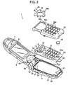
- FIG.2 is a disassembled perspective view of the lower housing 3 seen from the front.
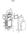
- FIG. 3 is a disassembled perspective view of the lower housing 3 seen from the back.
- the middle casing 31 is a main casing constituting the framework of the lower housing 3. Brackets 36 (Refer to FIG. 3) which support hinge units 41 are arranged in the form of protruding on the front face of the middle casing 31 at the coupling end to the upper housing 2.
- the hinge 4 is formed by pivotally coupling a pair of brackets 36, 36 (Refer to FIG.3) provided on the right and left ends of the front face of the middle casing 31 with a pair of right and left brackets 23, 23 (Refer to FIG.2) provided on the upper housing 2 (for example, on the back casing 22 of the upper housing 2) located within the brackets 36, 36 via the hinge units 41, 41.
- the hinge 4 is covered with hinge caps 42 and hinge covers 43 and 44. Specifically, the hinge caps 42, 42 cover the outer brackets 36, 36 on the middle casing 31.
- the hinge cover 43 covers the inner brackets 23, 23 on the upper housing 2 and a half of the space between the brackets 23, 23. Additionally, the hinge cover 44 covers the remaining half of the space.
- the hinge cover 43 is integrally formed with a logo plate 5 which is attached to the front casing 21 of the upper housing 2 and the hinge cover 44 is integrally formed with the key top plate 35 which constitutes a part of the front casing 32 of the lower housing 3.
- the space covered with the hinge covers 43 and 44 is used to pass an FPC (flexible printed circuit) 25 which connects circuits in the upper and lower bodies 2 and 3.
- the front face of the middle casing 31 is recessed as a board housing recess 37 except for the area in which the hinge 4 is provided.
- a circuit board 51 carrying wireless and control circuits is housed in the board housing recess 37. Un-shown fixed contact points are provided on the top surface of the circuit board 51 in positions corresponding to the direction indicator button 12, enter button 13, function buttons 14 and character/number input buttons 15.
- a sheet key 52 is overlapped on the circuit board 51.
- Movable contact points are provided on the bottom surface of the sheet key 52 at positions corresponding to the direction indicator button 12, enter button 13, function buttons 14 and character/number input buttons 15.
- a keypad 53 is placed onto the sheet key 52.
- the keypad 53 is made of an elastic rubber sheet, on the top surface of which are a protruding direction indicator button 12, an enter button 13, function buttons 14 and character/number input buttons 15.
- the keypad 53 also serves as watertight packing to prevent water from entering the board housing recess 37.
- the board housing recess 37 is covered and sealed with the keypad 53, which is provided with a hole 53a in which the waterproof telephone microphone 16 ispress fitted and by which the telephone microphone 16 is liquid-tightly held.
- the board housing recess 37 is covered with a front casing 32 housing the circuit board 51, sheet key 52 and keypad 53.
- the front casing 32 covers the middle casing 31 over the front face and sidewalls except for the area in which the hinge 4 is provided.
- the edge of the keypad 53 also serves as watertight packing and is inserted between the front casing 32 and middle casing 31 along the edge of the board housing recess 37.
- the front casing 32 is provided with multiple holes 32a corresponding to the character/number input buttons 15 which protrude through the holes 32a.
- the front casing 32 also is provided with a semicircle hole 32b for the key top plate 35 in the area where the direction indicator button 12, enter button 13 and function buttons 14 are provided.
- the key top plate 35 is provided with a hole 35a corresponding to the direction indicator button 12 in the center and notches 35b corresponding to the function buttons 14 along the circumference.
- the middle casing 31, back casing 33 and protective cover 34 are made of resin and the front casing 32 is made of metal, preferably a magnesium alloy.
- the magnesium alloy front casing 32 improves impact resistance and prevents the board circuit 51 and other components from being damaged due to impact.
- an antenna housing recess 38 and a battery housing recess 39 are formed during a state of recessing on the back face of the middle casing 31.
- the battery housing recess 39 is provided directly to the rear of the board housing recess 37.
- the antenna housing recess 38 is provided directly behind the hinge 4 by which the antenna housing recess 38 is positioned on the back face of the middle casing 31 in an area not directly behind the front casing 32 and board housing recess 37.
- the part 48 protruding from the hinge 4 into the antenna housing recess 38 is an extended space of the hinge 4 used to pass the FPC 25 from the hinge 4 to the board housing recess 37.
- An antenna 60 is housed in the antenna housing recess 38.
- This antenna 60 is a printed-wiring board type antenna.
- the antenna 60 is constituted by a board 61, a printed antenna 62 patterned on the board 61 and a chip antenna 63 on the board 61.
- FIG.4 is a cross-sectional view along the line IV-IV in FIG.1.
- a partition 40 which compartmentalizes the antenna housing recess 38 and board housing recess 37 is provided with a through-hole 40a which connects the antenna housing recess 38 and board housing recess 37.
- a wiring element 64 consisting of a wiring metal conductive element such as a coaxial cable and a plate is passed through the through-hole 40a to electrically connect the antenna 60 and circuit board 51.
- the partition 40 also is provided with a hole 40b to pass the FPC 25 in the area where the hinged area 4 is extended by the protruding part 48.
- the hole 40b is closed by watertight packing 26 attached to the FPC 25.
- watertight elastic rubber packing 65 is overlapped on the antenna 60 to cover and close the antenna housing recess 38.
- the antenna housing recess 38 is covered with the back casing 33 in the state of housing the antenna 60 by covering and closing by the watertight packing 65.
- the back casing 33 covers the middle casing 31 over the back face and sidewalls. The edge of the watertight packing 65 is clamped between the back and middle casings 33 and 31 along the edge of the antenna housing recess 38.
- the back casing 33 is provided with an opening 33a in the area corresponding to the battery housing recess 39.
- the rechargeable battery pack 17 is housed in the battery housing recess 39 through the opening 33a.
- a power connection terminal 55 provided on the circuit board 51 is exposed at the bottom of the batteryhousing recess 3 9 and makes contact with the terminal of the rechargeable battery pack 17.
- Watertight packing 56 is provided around the power connection terminal 55 to prevent water from entering the board housing recess 36 from the battery housing recess 39.
- the rechargeable battery pack 17 housed in the battery housing recess 39 is locked in the middle casing 31 by the lock mechanism 18.
- the back casing 33 is covered with the protective cover 34 in the area corresponding to the antenna housing recess 38.
- the protective cover 34 covers the back casing 33 and the sidewall of the middle casing 31 and is provided with a latch 34a which passes through a hole 33b formed in the back casing 33 and is latched to a locking part formed on the inner surface of the back casing 33.
- the front casing 32 is made of metal.
- the board housing recess 37 housing the circuit board 51 and the antenna housing recess 38 housing the antenna 60 are separately formed in the resin middle casing 31.
- the antenna housing recess 38 is covered with the resin back casing 33 which is separate from the front casing 32 covering the board housing recess 37 and the resin protective cover 34. Therefore, the antenna is not affected by the metal used in the front casing 32 during transmission and reception of radio waves thereby realizes excellent communication.
- the front casing 32 which covers the board housing recess 37 is metal, especially a product made from a Magnesium alloy, its impact resistance improves.
- edge of the keypad 53 also serving as watertight packing is inserted between the middle casing 31 and front casing 32 and the edge of the watertight packing 65 is inserted between the middle casing 31 and back casing 33, watertight properties improves.
- Embodiment 2 of the present invention is described hereafter with reference to FIGS. 5 to 11.
- FIG.5 is a perspective view of a folding-type mobile phone 101 in an embodiment of the mobile wireless device of the present invention when opened and seen from the front.
- FIG. 5 shows an upper housing 102, a lower housing 103 and a hinge 104 where the upper and lower housings 102 and 103 are pivotally coupled via the hinge 104.
- the upper housing 102 is formed by joining a front casing 121 and a back casing 122.
- the front face which meets the lower housing 103 in the folded state i.e. the front casing 121 side
- the lower housing 103 is formed by joining a front casing 132, a middle casing 131 (Refer to FIGS. 6 and 7) and a back casing 133.
- the front casing 132 which meets the upper housing 102 in the folded state is provided with an operation part 111, a telephone microphone 116 and a key top plate 135 constituting a part of the front casing 132.
- the operation part 111 comprises a direction indicator button 112 for cursor control and screen scrolling, an enter button 113, four function buttons 114 and 15 character/number input buttons 115.
- the casings including the front casing 132 and middle casing 131 are all made of resin.
- the hinge 104 is formed by pivotally coupling brackets 136, 136 provided on the middle casing 131 of the lower housing 103 to brackets 123, 123 provided on the back casing 122 of the upper housing 102 via hinge units 141, in which the outer brackets 136, 136 are covered with hinge caps 142.
- the space between the hinge caps 142, 142 is covered with a hinge cover 144 which is integrally formed with the key top plate 135, a hinge cover 145 (Refer to FIG.7) attached to the middle casing 131 of the lower housing 103, hinge covers 143, 143 which are integrally formed with the logo plate 105, and hinge covers 146, 147 (Refer to FIG. 7) attached to the back casing 122 of the upper housing 102.
- FIG.6 is a dissembled perspective view of the folding-type mobile phone 101 in the closed state seen from the back with a rechargeable the battery pack 117 removed.
- a battery housing recess 138 housing the rechargeable battery pack 117 is formed in the middle casing 131 of the lower housing 103.
- a lock mechanism 118 which locks the rechargeable battery pack 117 in the middle casing 131 and an informing speaker 119 are also provided in the middle casing 131 of the lower housing 103.
- FIG.7 shows the opened mobile phone 101 of FIG.5 with the logo plate 105 integrally formed with the hinge covers 143, 143, key top plate 135 integrally formed with the hinge cover 114, hinge caps 142, front casing 132 of the lowerhousing 103, connector cover 120 and the internal modules which are removed.
- numeral 145 refers to a hinge cover attached to the middle casing 131 of the lower housing 102.
- Numerals 145, 146 refer to hinge covers attached to the back casing 122 of the upper housing 102, with the hinge covers 146, 147 being integrally formed.
- the board housing recess 137 is formed in the middle casing 131 of the lower housing 103 and a packing groove 131a is formed on the top surface of the sidewall of the board housing recess 137.
- the end wall of the board housing recess 137 on the hinge 104 side is provided with right and left holes.
- the left hole 131b communicates to an antenna housing recess 138 which is described later, and an antenna connection conductor 164 protrudes through the hole 131b.
- the right hole 131c communicates to the hinge 104 and is used to pass an FPC 125 which connects circuits in the upper body 102 and lower body 103.
- the end wall of the back casing 122 on the hinge 104 side is provided with a hole 122a through which to pass the FPC 125.
- a speaker mounting part 131d, an internal mechanism 118a for the lock mechanism 118 and a vibrator 157 for informing call reception are provided on the inner surface of the middle casing 131.
- FIG.8 shows the closed mobile phone 101 of FIG.6 with the rechargeable batterypack 117, back casing 133 of the lower housing 103, hinge caps 142 and protective cover 134 removed.
- the antenna housing recess 138 is formed in the middle casing 131 of the lower housing 103 along the end on the hinge 104 side behind the hinge 104 and hole 131b being open to the antenna housing recess 138. Therefore, one end of the antenna connection conductor 164 protrudes into the antenna housing recess 138.
- An antenna board fixing surface 138a in one half in the transverse direction and an antenna support rib 138b in the other half is formed in the inside of the antenna housing recess 138.
- the antenna fixing surface 138a and antenna support rib 138b are at the same level and an antenna 160 is mounted thereon.
- a packing groove 138c is formed on the top surface of the sidewall of the antenna housing recess 138 and watertight packing 165 is provided in the packing groove 138c.
- the antenna 160 is a meander line patterned linear antenna on a rigid board (a hard printed board) 161 as shown in the figure.
- Meander line patterned copper foil antenna elements 162b, 162c are formed from a power supply electrode 162a on either side thereof on the board 161.
- the left thicker meander line antenna element 162b is used for communication and the right thicker meander line antenna element 162c is used for GPS (Global positioning system). Both are modified monopole antennas.
- the board 161 is provided with an integrated spring connector 167 which protrudes on the surface aide opposite to power supply electrode 162a.
- the watertight packing 165 is provided on its circumference with a seal lip 165a corresponding to the packing groove 138c.
- the antenna connection conductor 164 is formed by molding a resin 164b with a metal plate 164a as shown in FIGS. 11A and 11B. More specifically, the antenna connection conductor 164 is constituted as a forming component in which the metal plate 164a is inserted into the resin 164b by insert molding.
- the antenna connection conductor 164 has, as shown in the figure, a nearly L-shape and comprises a circuit board side connection terminal 164c at one end where the metal plate 164a is exposed (Refer to FIG.11). As shown FIG.11B, the other end of the molded resin 164b opposite the circuit board side connection terminal 164c is provided with a small hole 164d. The part of the metal plate 164 which is exposed in the small hole 164d serves as an antenna connection terminal 164e.
- the antenna connection conductor 164 is passed through the hole 131b formed in the end wall of the board housing recess 137 on the hinge 104 side.
- the antenna connection conductor 164 is passed through the hole 131b formed in the partition wall which compartmentalizes the board housing recess 137, and the hinge 104 and antenna housing recess 138.
- the half portion of the circuit board side connection terminal 164c side is located near a vibrator 157.
- the circuit board side connection terminal 164c is located away from the vibrator 157 as shown in the figure.
- the half portion of the antenna connection terminal 164e side is located within the antenna housing recess 138.
- the antenna connection terminal 164e is located near the antenna fixing surface 138a as shown in the figure.
- the antenna 160 is inserted into the antenna housing recess 138.
- the spring connector 167 is connected to the antenna side connection terminal 164e and one half of the antenna 160 is bonded to the antenna fixing surface 138a, for example, using a double-sided adhesive tape.
- the other half of the antenna 160 is supported by the antenna support rib 41b.
- the seal lip 165a of the watertight packing 165 is fitted in the packing groove 138c around the antenna housing recess 138 so as to cover the antenna housing recess 138 with the watertight packing 165.
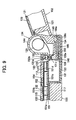
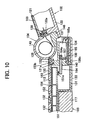
- FIGS. 9 and 10 show a cross-section of the hinge 104 side.
- a circuit board 151 electronic parts 151a, 151b and 151c, a connector 151d, a module frame (shield casing) 154, a sheet key 152, a keypad 153, a contact spring 151e, an FPC 125, a watertight cap 126, a connector 127 and a watertight cap 128.
- the module frame 154 is provided to reinforce and electromagnetically shield the circuit board made of metal such as a magnesium alloy.
- the seal lip 153b along the circumference of the keypad 153 is fitted in the packing groove 131a formed on the sidewall of the board housing recess 137.
- the circuit board side connection terminal 164c of the antenna connection conductor 164 is connected to a high frequency input/output point of a wireless circuit mounted on the circuit board 151.
- an antenna power supply point via the contact spring 151e is connected to a high frequency input/output point of a wireless circuit mounted on the circuit board 151.
- the FPC 125 is provided in the space covered by the hinge covers 143 and 144 and the FPC 125 connects the circuit board 151 in the lower housing 103 with the circuit board in the upper housing 102.
- one end of the FPC 125 emerges from the hole 131c via the watertight cap 126 and the connecter 127 provided at this end is connected to the connector 151d on the circuit board 151.
- the other end of the FPC 125 emerges from the hole 122a via the watertight cap 128 and is connected to an un-shown circuit board in the upper housing 102.
- the antenna 160 is positioned behind the hinge 104.
- the antenna on the antenna board 161, specifically the linear antenna elements 162b and 162c, is provided on the surface of the antenna board 161 away from the hinge 104 for receiving less influence from the FPA 125.
- the linear antenna elements 162b and 162c on the antenna board 161 are connected to the high frequency input/output point (power supply point) of a wireless circuit part installed on the circuit board 151 via the antenna connection conductor 164 as an electric conductor.
- the antenna electric current through the antenna connection conductor 164 is maximized near the power supply point.
- the antenna connection conductor 164 is extended along the longitudinal direction of the housing (the vertical direction while making a call) in the vicinity of the power supply point so that the antenna connection conductor 164 serves as a monopole antenna which constitutes a hybrid antenna together with the antenna 160.
- the monopole part contributes to transmission/reception of vertically-polarized wave components and the gain of vertically-polarized wave components rises.
- the antenna connection conductor 164 has, as shown in FIGS. 11A and 11B, a nearly L shape, one end of which is placed in the antenna housing recess 138 behind the hinge 104 and connected to the spring connector 167 of the antenna 160 (Refer to FIGS. 8 and 10).
- the other half portion side of the antenna connection conductor 164 is extended into the board housing recess 137 through the hole 131b formed in the partition 140 (the sidewall of the antenna housing recess 138) which compartmentalizes the antenna housing recess 138 and the board housing recess 137 housing the circuit board 151, etc. and connected to the contact spring 151e on the circuit board 151 (Refer to FIGS. 7 and 10).
- the contact spring 151e is connected to the wireless circuit part installed on the circuit board 151 and serves as a high frequency input/output point (antenna power supply point).
- the metal plate 164a of the antenna connection conductor 164, spring connector 167 and linear antennas on the antenna board 161 together constitute a quarter-wavelength antenna.
- connection terminal 164c side of the antenna connection conductor 164 is extended in the longitudinal direction of the lower housing 103 and the antenna connection conductor 164 functions as a monopole antenna.
- the linear antenna element 162b on the antenna board 161 does not need to be of a quarter-wavelength and the antenna board 161 can be down-sized. Then, the antenna board 161 (antenna 160) can be provided in the lower housing 103 behind the hinge 104 where it is difficult to reserve a longitudinally sufficient space.
- the lower housing 103 can be down-sized without providing projections on either side of the hinge.
- the reduction in gain of vertically-polarized wave components as a result of down-sizing the antenna board 161 (antenna 160) having the linear antenna element 162b as a built-in antenna can be compensated for by the antenna connection conductor 164 constituting a hybrid antenna together with the down-sized antenna 160.
- the gain of vertically-polarized wave components can be increased.
- the electrical length of the linear antenna part (communication linear antenna part) on the antenna board 161 and the antenna connection conductor 164 is desirably an eighth of the communication band wavelength.
- nearly an eighth is acceptable for sufficient function.
- the monopole antenna part achieves excellent transmission/reception of vertically-polarized wave components even if it is provided with an electrical length smaller than an eighth but nearly an eighth of the communication band wavelength. Then, the gain of vertically-polarized wave components is increased.
- the vibrator 157 is provided near the antenna connection conductor 164.
- the antenna connection conductor 164 is turned away from the vibrator. Therefore, the influence of the vibrator 157 on the antenna connection conductor 164 is minimized.
- the metal plate 164a part of the antenna connection conductor 164 which connects the antenna connection terminal 164e part and the circuit board connection terminal, namely the metal plate 164a part extended in the longitudinal direction of the lower housing 103, is molded at the furthermost point form the vibrator 157.
- one half portion side of the antenna connection conductor 164 in the antenna housing recess 138 behind the hinge 104 is positioned near the partition side which compartmentalizes the antenna housing recess 138 and the board housing recess 137 while receiving little influence from the FPC 125.
- the metal module frame 154 is housed in the board housing recess 137.
- the board housing recess 137 housing the circuit board 151 and the antenna housing recess 138 housing the antenna 160 are separately formed in the resin middle casing 131.
- the antenna housing recess 138 is covered with the resin back casing 133 and resin protective cover 134. Therefore, the antenna receives very little influence from the metal used in the module frame 154 during transmission/reception of radio waves thereby realizing excellent communication.
- the antenna connection conductor 164 connecting the antenna 160 and the circuit board 151 serves as a monopole antenna and increases the gain of vertically-polarized wave components which allows for down-sizing of the antenna 160 housed in the antenna housing recess 138.
- a similar effect can be obtained by an antenna connection conductor made of a metal plate or a metal wire without resin molding in place of the structure of the embodiment.
- the edge of the keypad 153 also serving as watertight packing is inserted between the middle casing 131 and front casing 132 and the edge of the watertight packing 165 is inserted between the middle casing 131 and back casing 133, thereby improving watertight properties.
- the upper housing contains the telephone speaker and display and the lower housing contains the telephone microphone and operation part.
- the upper housing contains the telephone speaker and the lower housing contains the telephone microphone or the upper housing contains the display and the lower housing contains the operation part can be provided.
- the hinge cover and front casing are separate pieces. However, they can be integrally formed. Similarly, the back casing and protective cover can be integrally formed.
- the present invention is applied to a folding-type mobile phone.
- the present invention can be applied to any mobile wireless device which is provided with a built-in antenna and performs transmission and/or reception using the antenna, such as laptop computers, wave clocks, pager, and PDAs (personal digital assistances). These devices are not necessarily of a folding-type.
Landscapes
- Engineering & Computer Science (AREA)
- Signal Processing (AREA)
- Computer Networks & Wireless Communication (AREA)
- Telephone Set Structure (AREA)
- Mobile Radio Communication Systems (AREA)
- Casings For Electric Apparatus (AREA)
- Transceivers (AREA)
Abstract
Description
- This application is based upon and claims the benefit of priority from the prior Japanese Patent Application No. 2004-334603 filed November 18, 2004, Japanese Patent Application No. 2005-211695 filed July 21, 2005 and Japanese Patent Application No. 2005-325218 filed November 9, 2005, the entire contents of which is incorporated herein by reference.
- The present invention relates to a mobile wireless device, in particular to a mobile wireless device having a built-in antenna.
- As a mobile wireless device, mobile phones are widely used. Some of them have a built-in antenna (reference is made, for example, to Japanese Laid-Open Patent Application No. 2003-8320 and Japanese Laid-Open Patent Application No.2004-297535).
- The casing of the housing, particularly the front casing having holes for the operating buttons of some mobile phones, is made of metal such as a magnesium alloy which is lightweight and having high specific strength for providing the housing with improved impact resistance (reference is made, for example, to Japanese Laid-Open Patent Application No. 2001-292208 (WO International Publication No.01/58116 A1). The mobile phone described in Japanese Laid-Open Patent Application No. 2001-292208 is provided with circuit module reinforcement and an electromagnetic shielding member, also made of metal such as magnesium alloy.
- However, when a built-in antenna is provided in the housing, the antenna is usually mounted on a circuit board. When a metal front casing of housing, a metal circuit module reinforcement member or an electromagnetic shielding member is used, there are problems in that the metal provided near the antenna deteriorates the transmission and reception properties of the antenna.
- The present invention is proposed to resolve the above problem and is provided with the object of providing a mobile wireless device that maintains the transmission and/or reception properties of the built-in antenna in an excellent state, even if any of the front casing of housing, circuit module reinforcement member, and circuit module electromagnetic shielding member is made of metal.
- In order to achieve the above object, the present invention provides a mobile wireless device having a built-in antenna in the housing, comprising the housing having a first resin casing in which a first housing recess which houses a circuit board and a second housing recess which houses the antenna are separately formed, the first housing recess is covered with a second resin or metal casing with the circuit board housed therein, the second housing recess is covered with a third resin casing with the antenna housed therein.
- The present invention ensures that the transmission and/or reception properties of the antenna are well maintained even if the second casing is a metal casing or if the circuit board is provided with a metal reinforcement member or a metal electromagnetic shielding member.
- When the second casing is a metal casing, the housing is provided with improved strength, protecting the housed circuit board against impact and shock in addition to the above effect.
- The above and further objects and novel features of the present invention will more fully appear from the following detailed description when the same is read in conjunction with the accompanying drawings. Itisto be expressly understood,however, that the drawings are for the purpose of illustration only and are not intended as a definition of the limits of the invention.
-
- FIGS. 1A to 1C show the structure of a mobile phone in an embodiment of the mobile wireless device to which the present invention is applied. FIG.1A is a side view of the
mobile phone 1, FIG.1B is a front view of themobile phone 1 and FIG.1C is a rear view of themobile phone 1; - FIG.2 is a disassembled perspective view of the
mobile phone 1 seen from the front with thelower housing 3 being disassembled; - FIG. 3 is a disassembled perspective view of the
lower housing 3 seen from the back with thelower housing 3 being disassembled; - FIG. 4 is a cross-sectional view along the line IV-IV in FIG. 1;
- FIG.5 is a perspective view showing the structure of a folding-type mobile phone as second embodiment of the mobile wireless device to which the present invention is applied when seen from the front;
- FIG. 6 is a disassembled perspective view of the folding-type mobile phone of FIG.5 in the closed state seen from the back with the battery pack removed;
- FIG.7 is a perspective view of the opened mobile phone of FIG.5 with the front casing, hinge cap, hinge cover and internal modules of the lower housing removed;
- FIG.8 is a perspective view of the closed mobile phone of FIG.6 with the battery pack, back casing and hinge caps of the lower housing removed in order to explain the structure of the antenna;
- FIG. 9 is a cross-sectional·view of the hinge corresponding to the area covered with the hinge cover integrally formed with the key top plate of FIG.5;
- FIG. 10 is a cross-sectional view of the hinge corresponding to the area covered with the hinge cover integrally formed with the logo plate of FIG.5; and
- FIGS. 11A and 11B are illustrations showing the antenna connection conductor. FIG.11A is a perspective view seen from the same direction as FIG.7. FIG.11B is a perspective view seen from the same direction as FIG.8.
- Preferred embodiments of the present invention are described hereafter with reference to the drawings. Embodiments described below include various technically preferable restrictions to implementing the present invention. However, the scope of the present invention is not restricted to the embodiments and illustrations discussed below.
- FIGS. 1A to 1C show three sides of a
mobile phone 1 in an embodiment of the mobile wireless device to which the present invention is applied. FIG.1A is a side view, FIG.1B is a front view and FIG.1C is a rear view. - The
mobile phone 1 of this embodiment is of a folding-type provided with anupper housing 2 pivotally coupled to alower housing 3 via ahinge 4 which allows the upper andlower housings - The
upper housing 2 comprises afront casing 21 and aback casing 22. Of the front and back faces of theupper housing 2, the front face which goes inside when folded (i.e. thefront casing 21 side) is provided with amain display 6 consisting of a liquid crystal display panel or an electro-luminescence display panel. Atelephone speaker 7 is provided in theupper housing 2 further away from thehinge 4 than themain display 6. - In the
upper housing 2, the back face opposite the front face provided with the main display 6 (i.e. theback casing 22 side) is provided with asub-display 8 consisting of a liquid crystal display panel or an electro-luminescence display panel. Animaging lens 9 is provided near thesub-display 8. A solid-state imaging element such as a CCD (charge-coupled device) type or CMOS (complementary metal oxide semiconductor) type is provided in theupper housing 2 at a point on the optical axis of theimaging lens 9 where an image of an object is formed on the solid-state imaging element by theimaging lens 9. Aflash light 10 consisting of a light emitting element such as an LED (light emitting diode) is provided near theimaging lens 9 and is turned on at the time of imaging. - The
lower housing 3 comprises amiddle casing 31 having the main casing constituting the framework of the lower housing 3 (Refer to FIGS. 2 and 3) , a front casing (front cover) 32 which covers the front face of themiddle casing 31, a back casing (back cover) 33 which covers the back face of themiddle casing 31, aprotective cover 34 which partially covers themiddle casing 31 andback casing 33 near thehinge 4, and akey top plate 35 which constitutes a part of thefront casing 32. - Of the faces of the
lower housing 3, the front face which goes inside when folded (i. e. thefront casing 32 side) is provided with anoperation part 11. Theoperation part 11 comprises adirection indicator button 12 for cursor control and screen scrolling, anenter button 13 in the center of thedirection indicator button 12, fourfunction buttons 14 around thedirection indicator button number input buttons 15 below thedirection indicator button 12. In addition, atelephone microphone 16 is provided in thelower housing 3 further away from thehinge 4 than theoperation part 11. - A
rechargeable battery pack 17 is detachably provided in thelower housing 3 on the back face opposite the front face holding the operation part 11 (i.e. theback casing 33 side) in which alock mechanism 18 which locks therechargeable battery pack 17 in thelower housing 3 is also provided. - The internal structure of the
lower housing 3 is described in detail hereafter with reference to FIGS. 2 and 3. FIG.2 is a disassembled perspective view of thelower housing 3 seen from the front. FIG. 3 is a disassembled perspective view of thelower housing 3 seen from the back. - The
middle casing 31 is a main casing constituting the framework of thelower housing 3. Brackets 36 (Refer to FIG. 3) which supporthinge units 41 are arranged in the form of protruding on the front face of themiddle casing 31 at the coupling end to theupper housing 2. - The
hinge 4 is formed by pivotally coupling a pair ofbrackets 36, 36 (Refer to FIG.3) provided on the right and left ends of the front face of themiddle casing 31 with a pair of right andleft brackets 23, 23 (Refer to FIG.2) provided on the upper housing 2 (for example, on theback casing 22 of the upper housing 2) located within thebrackets hinge units - The
hinge 4 is covered with hinge caps 42 and hinge covers 43 and 44. Specifically, the hinge caps 42, 42 cover theouter brackets middle casing 31. The hinge cover 43 covers theinner brackets upper housing 2 and a half of the space between thebrackets hinge cover 44 covers the remaining half of the space. - In this embodiment, the
hinge cover 43 is integrally formed with alogo plate 5 which is attached to thefront casing 21 of theupper housing 2 and thehinge cover 44 is integrally formed with the keytop plate 35 which constitutes a part of thefront casing 32 of thelower housing 3. The space covered with the hinge covers 43 and 44 is used to pass an FPC (flexible printed circuit) 25 which connects circuits in the upper andlower bodies - As shown in FIG.2, the front face of the
middle casing 31 is recessed as aboard housing recess 37 except for the area in which thehinge 4 is provided. - A
circuit board 51 carrying wireless and control circuits is housed in theboard housing recess 37. Un-shown fixed contact points are provided on the top surface of thecircuit board 51 in positions corresponding to thedirection indicator button 12,enter button 13,function buttons 14 and character/number input buttons 15. - A
sheet key 52 is overlapped on thecircuit board 51. Movable contact points are provided on the bottom surface of thesheet key 52 at positions corresponding to thedirection indicator button 12,enter button 13,function buttons 14 and character/number input buttons 15. - A
keypad 53 is placed onto thesheet key 52. Thekeypad 53 is made of an elastic rubber sheet, on the top surface of which are a protrudingdirection indicator button 12, anenter button 13,function buttons 14 and character/number input buttons 15. Thekeypad 53 also serves as watertight packing to prevent water from entering theboard housing recess 37. Theboard housing recess 37 is covered and sealed with thekeypad 53, which is provided with ahole 53a in which thewaterproof telephone microphone 16 ispress fitted and by which thetelephone microphone 16 is liquid-tightly held. - The
board housing recess 37 is covered with afront casing 32 housing thecircuit board 51,sheet key 52 andkeypad 53. Thefront casing 32 covers themiddle casing 31 over the front face and sidewalls except for the area in which thehinge 4 is provided. The edge of thekeypad 53 also serves as watertight packing and is inserted between thefront casing 32 andmiddle casing 31 along the edge of theboard housing recess 37. - The
front casing 32 is provided withmultiple holes 32a corresponding to the character/number input buttons 15 which protrude through theholes 32a. Thefront casing 32 also is provided with asemicircle hole 32b for the keytop plate 35 in the area where thedirection indicator button 12,enter button 13 andfunction buttons 14 are provided. The keytop plate 35 is provided with ahole 35a corresponding to thedirection indicator button 12 in the center andnotches 35b corresponding to thefunction buttons 14 along the circumference. Hence, when the keytop plate 35 is installed in thehole 32b of thefront casing 32, thedirection indicator button 12 and theenter button 13 protrude from thehole 35a formed in the keytop plate 35 andfunction buttons 14 protrude from thenotches 35b formed in the keytop plate 35. - In this embodiment, the
middle casing 31, back casing 33 andprotective cover 34 are made of resin and thefront casing 32 is made of metal, preferably a magnesium alloy. Using the magnesiumalloy front casing 32 improves impact resistance and prevents theboard circuit 51 and other components from being damaged due to impact. - As shown in FIG. 3, an
antenna housing recess 38 and abattery housing recess 39 are formed during a state of recessing on the back face of themiddle casing 31. Thebattery housing recess 39 is provided directly to the rear of theboard housing recess 37. Theantenna housing recess 38 is provided directly behind thehinge 4 by which theantenna housing recess 38 is positioned on the back face of themiddle casing 31 in an area not directly behind thefront casing 32 andboard housing recess 37. - In FIG.3, the
part 48 protruding from thehinge 4 into theantenna housing recess 38 is an extended space of thehinge 4 used to pass theFPC 25 from thehinge 4 to theboard housing recess 37. - An
antenna 60 is housed in theantenna housing recess 38. Thisantenna 60 is a printed-wiring board type antenna. As shown in FIG.4, theantenna 60 is constituted by aboard 61, a printedantenna 62 patterned on theboard 61 and achip antenna 63 on theboard 61. FIG.4 is a cross-sectional view along the line IV-IV in FIG.1. - In the
middle casing 31, apartition 40 which compartmentalizes theantenna housing recess 38 andboard housing recess 37 is provided with a through-hole 40a which connects theantenna housing recess 38 andboard housing recess 37. - A
wiring element 64 consisting of a wiring metal conductive element such as a coaxial cable and a plate is passed through the through-hole 40a to electrically connect theantenna 60 andcircuit board 51. - The
partition 40 also is provided with ahole 40b to pass theFPC 25 in the area where the hingedarea 4 is extended by the protrudingpart 48. Thehole 40b is closed by watertight packing 26 attached to theFPC 25. - As shown in FIG.3, watertight elastic rubber packing 65 is overlapped on the
antenna 60 to cover and close theantenna housing recess 38. Theantenna housing recess 38 is covered with theback casing 33 in the state of housing theantenna 60 by covering and closing by thewatertight packing 65. Theback casing 33 covers themiddle casing 31 over the back face and sidewalls. The edge of thewatertight packing 65 is clamped between the back andmiddle casings antenna housing recess 38. - The
back casing 33 is provided with anopening 33a in the area corresponding to thebattery housing recess 39. Therechargeable battery pack 17 is housed in thebattery housing recess 39 through theopening 33a. Apower connection terminal 55 provided on thecircuit board 51 is exposed at the bottom of thebatteryhousing recess 3 9 and makes contact with the terminal of therechargeable battery pack 17. - Watertight packing 56 is provided around the
power connection terminal 55 to prevent water from entering theboard housing recess 36 from thebattery housing recess 39. Therechargeable battery pack 17 housed in thebattery housing recess 39 is locked in themiddle casing 31 by thelock mechanism 18. - The
back casing 33 is covered with theprotective cover 34 in the area corresponding to theantenna housing recess 38. Theprotective cover 34 covers theback casing 33 and the sidewall of themiddle casing 31 and is provided with alatch 34a which passes through ahole 33b formed in theback casing 33 and is latched to a locking part formed on the inner surface of theback casing 33. - As described above, in this embodiment, the
front casing 32 is made of metal. Theboard housing recess 37 housing thecircuit board 51 and theantenna housing recess 38 housing theantenna 60 are separately formed in the resinmiddle casing 31. Furthermore, theantenna housing recess 38 is covered with the resin back casing 33 which is separate from thefront casing 32 covering theboard housing recess 37 and the resinprotective cover 34. Therefore, the antenna is not affected by the metal used in thefront casing 32 during transmission and reception of radio waves thereby realizes excellent communication. - On the other hand, since the
front casing 32 which covers theboard housing recess 37 is metal, especially a product made from a Magnesium alloy, its impact resistance improves. - Furthermore, since the edge of the
keypad 53 also serving as watertight packing is inserted between themiddle casing 31 andfront casing 32 and the edge of thewatertight packing 65 is inserted between themiddle casing 31 and back casing 33, watertight properties improves. -
Embodiment 2 of the present invention is described hereafter with reference to FIGS. 5 to 11. - FIG.5 is a perspective view of a folding-type
mobile phone 101 in an embodiment of the mobile wireless device of the present invention when opened and seen from the front. FIG. 5 shows anupper housing 102, alower housing 103 and ahinge 104 where the upper andlower housings hinge 104. - The
upper housing 102 is formed by joining afront casing 121 and aback casing 122. The front face which meets thelower housing 103 in the folded state (i.e. thefront casing 121 side) is provided with a display (liquid crystal display screen) 106, atelephone speaker 107 and alogo plate 105. - The
lower housing 103 is formed by joining afront casing 132, a middle casing 131 (Refer to FIGS. 6 and 7) and aback casing 133. Thefront casing 132 which meets theupper housing 102 in the folded state is provided with anoperation part 111, a telephone microphone 116 and a keytop plate 135 constituting a part of thefront casing 132. Theoperation part 111 comprises adirection indicator button 112 for cursor control and screen scrolling, anenter button 113, fourfunction buttons number input buttons 115. In this embodiment, the casings including thefront casing 132 andmiddle casing 131 are all made of resin. - The
hinge 104 is formed by pivotally couplingbrackets middle casing 131 of thelower housing 103 tobrackets back casing 122 of theupper housing 102 viahinge units 141, in which theouter brackets hinge cover 144 which is integrally formed with the keytop plate 135, a hinge cover 145 (Refer to FIG.7) attached to themiddle casing 131 of thelower housing 103, hinge covers 143, 143 which are integrally formed with thelogo plate 105, and hinge covers 146, 147 (Refer to FIG. 7) attached to theback casing 122 of theupper housing 102. - FIG.6 is a dissembled perspective view of the folding-type
mobile phone 101 in the closed state seen from the back with a rechargeable thebattery pack 117 removed. Abattery housing recess 138 housing therechargeable battery pack 117 is formed in themiddle casing 131 of thelower housing 103. Alock mechanism 118 which locks therechargeable battery pack 117 in themiddle casing 131 and an informingspeaker 119 are also provided in themiddle casing 131 of thelower housing 103. - A
power connection terminal 155 provided on acircuit board 151, described later, is exposed in thebattery housing recess 138 withwatertight packing 156 provided around thepower connection terminal 155. Theback casing 133 provided with anopening 133a corresponding to therechargeable battery pack 117, aconnector cover 120 and aprotective cover 134 is attached to themiddle casing 131. - FIG.7 shows the opened
mobile phone 101 of FIG.5 with thelogo plate 105 integrally formed with the hinge covers 143, 143, keytop plate 135 integrally formed with thehinge cover 114, hinge caps 142,front casing 132 of thelowerhousing 103,connector cover 120 and the internal modules which are removed. In the figure, numeral 145 refers to a hinge cover attached to themiddle casing 131 of thelower housing 102.Numerals back casing 122 of theupper housing 102, with the hinge covers 146, 147 being integrally formed. - As shown in the figure, the
board housing recess 137 is formed in themiddle casing 131 of thelower housing 103 and apacking groove 131a is formed on the top surface of the sidewall of theboard housing recess 137. The end wall of theboard housing recess 137 on thehinge 104 side is provided with right and left holes. The left hole 131b communicates to anantenna housing recess 138 which is described later, and anantenna connection conductor 164 protrudes through the hole 131b. Theright hole 131c communicates to thehinge 104 and is used to pass anFPC 125 which connects circuits in theupper body 102 andlower body 103. In theupper housing 102, the end wall of theback casing 122 on thehinge 104 side is provided with ahole 122a through which to pass theFPC 125. - A speaker mounting part 131d, an
internal mechanism 118a for thelock mechanism 118 and avibrator 157 for informing call reception are provided on the inner surface of themiddle casing 131. - FIG.8 shows the closed
mobile phone 101 of FIG.6 with therechargeable batterypack 117, back casing 133 of thelower housing 103, hinge caps 142 andprotective cover 134 removed. - As shown in the figure, the
antenna housing recess 138 is formed in themiddle casing 131 of thelower housing 103 along the end on thehinge 104 side behind thehinge 104 and hole 131b being open to theantenna housing recess 138. Therefore, one end of theantenna connection conductor 164 protrudes into theantenna housing recess 138. - An antenna
board fixing surface 138a in one half in the transverse direction and anantenna support rib 138b in the other half is formed in the inside of theantenna housing recess 138. Theantenna fixing surface 138a andantenna support rib 138b are at the same level and anantenna 160 is mounted thereon. - A packing
groove 138c is formed on the top surface of the sidewall of theantenna housing recess 138 andwatertight packing 165 is provided in thepacking groove 138c. - The
antenna 160 is a meander line patterned linear antenna on a rigid board (a hard printed board) 161 as shown in the figure. Meander line patterned copperfoil antenna elements power supply electrode 162a on either side thereof on theboard 161. In FIG.8, the left thicker meanderline antenna element 162b is used for communication and the right thicker meanderline antenna element 162c is used for GPS (Global positioning system). Both are modified monopole antennas. - The
board 161 is provided with anintegrated spring connector 167 which protrudes on the surface aide opposite topower supply electrode 162a. - The
watertight packing 165 is provided on its circumference with aseal lip 165a corresponding to thepacking groove 138c. - The
antenna connection conductor 164 is formed by molding aresin 164b with ametal plate 164a as shown in FIGS. 11A and 11B. More specifically, theantenna connection conductor 164 is constituted as a forming component in which themetal plate 164a is inserted into theresin 164b by insert molding. - In this embodiment, the
antenna connection conductor 164 has, as shown in the figure, a nearly L-shape and comprises a circuit boardside connection terminal 164c at one end where themetal plate 164a is exposed (Refer to FIG.11). As shown FIG.11B, the other end of the moldedresin 164b opposite the circuit boardside connection terminal 164c is provided with asmall hole 164d. The part of themetal plate 164 which is exposed in thesmall hole 164d serves as anantenna connection terminal 164e. - The installation of the
antenna connection conductor 164 andantenna 160 is described hereafter. - As shown in FIG.7, the
antenna connection conductor 164 is passed through the hole 131b formed in the end wall of theboard housing recess 137 on thehinge 104 side. In other words, theantenna connection conductor 164 is passed through the hole 131b formed in the partition wall which compartmentalizes theboard housing recess 137, and thehinge 104 andantenna housing recess 138. The half portion of the circuit boardside connection terminal 164c side is located near avibrator 157. However, the circuit boardside connection terminal 164c is located away from thevibrator 157 as shown in the figure. - As shown in FIG. 8, the half portion of the
antenna connection terminal 164e side is located within theantenna housing recess 138. Theantenna connection terminal 164e is located near theantenna fixing surface 138a as shown in the figure. - Then, the
antenna 160 is inserted into theantenna housing recess 138. Thespring connector 167 is connected to the antennaside connection terminal 164e and one half of theantenna 160 is bonded to theantenna fixing surface 138a, for example, using a double-sided adhesive tape. Here, the other half of theantenna 160 is supported by the antenna support rib 41b. - Then, the
seal lip 165a of thewatertight packing 165 is fitted in thepacking groove 138c around theantenna housing recess 138 so as to cover theantenna housing recess 138 with thewatertight packing 165. - FIGS. 9 and 10 show a cross-section of the
hinge 104 side. In the figures shown are acircuit board 151,electronic parts connector 151d, a module frame (shield casing) 154, asheet key 152, akeypad 153, acontact spring 151e, anFPC 125, awatertight cap 126, a connector 127 and awatertight cap 128. Themodule frame 154 is provided to reinforce and electromagnetically shield the circuit board made of metal such as a magnesium alloy. - The
seal lip 153b along the circumference of thekeypad 153 is fitted in thepacking groove 131a formed on the sidewall of theboard housing recess 137. - As shown in FIG.10, in the
board housing recess 137, the circuit boardside connection terminal 164c of theantenna connection conductor 164 is connected to a high frequency input/output point of a wireless circuit mounted on thecircuit board 151. In other words, an antenna power supply point via thecontact spring 151e. - As shown in the figure, the
FPC 125 is provided in the space covered by the hinge covers 143 and 144 and theFPC 125 connects thecircuit board 151 in thelower housing 103 with the circuit board in theupper housing 102. - Specifically, as shown in FIG. 9, one end of the
FPC 125 emerges from thehole 131c via thewatertight cap 126 and the connecter 127 provided at this end is connected to theconnector 151d on thecircuit board 151. - As shown in FIG.10, the other end of the
FPC 125 emerges from thehole 122a via thewatertight cap 128 and is connected to an un-shown circuit board in theupper housing 102. - Consequently, as shown in FIGS. 8 to 10, the
antenna 160 is positioned behind thehinge 104. - The antenna on the
antenna board 161, specifically thelinear antenna elements antenna board 161 away from thehinge 104 for receiving less influence from theFPA 125. - The
linear antenna elements antenna board 161 are connected to the high frequency input/output point (power supply point) of a wireless circuit part installed on thecircuit board 151 via theantenna connection conductor 164 as an electric conductor. - The antenna electric current through the
antenna connection conductor 164 is maximized near the power supply point. - In this embodiment, the
antenna connection conductor 164 is extended along the longitudinal direction of the housing (the vertical direction while making a call) in the vicinity of the power supply point so that theantenna connection conductor 164 serves as a monopole antenna which constitutes a hybrid antenna together with theantenna 160. - Therefore, the monopole part contributes to transmission/reception of vertically-polarized wave components and the gain of vertically-polarized wave components rises.
- Additionally, the
antenna connection conductor 164 has, as shown in FIGS. 11A and 11B, a nearly L shape, one end of which is placed in theantenna housing recess 138 behind thehinge 104 and connected to thespring connector 167 of the antenna 160 (Refer to FIGS. 8 and 10). The other half portion side of theantenna connection conductor 164 is extended into theboard housing recess 137 through the hole 131b formed in the partition 140 (the sidewall of the antenna housing recess 138) which compartmentalizes theantenna housing recess 138 and theboard housing recess 137 housing thecircuit board 151, etc. and connected to thecontact spring 151e on the circuit board 151 (Refer to FIGS. 7 and 10). Thecontact spring 151e is connected to the wireless circuit part installed on thecircuit board 151 and serves as a high frequency input/output point (antenna power supply point). - Accordingly, in this embodiment, the
metal plate 164a of theantenna connection conductor 164,spring connector 167 and linear antennas on theantenna board 161 together constitute a quarter-wavelength antenna. - In the state where the
antenna connection conductor 164 having a nearly L shape is set in the hole 131b, theconnection terminal 164c side of theantenna connection conductor 164 is extended in the longitudinal direction of thelower housing 103 and theantenna connection conductor 164 functions as a monopole antenna. - Therefore, the
linear antenna element 162b on theantenna board 161 does not need to be of a quarter-wavelength and theantenna board 161 can be down-sized. Then, the antenna board 161 (antenna 160) can be provided in thelower housing 103 behind thehinge 104 where it is difficult to reserve a longitudinally sufficient space. - Consequently, the
lower housing 103 can be down-sized without providing projections on either side of the hinge. - The reduction in gain of vertically-polarized wave components as a result of down-sizing the antenna board 161 (antenna 160) having the
linear antenna element 162b as a built-in antenna can be compensated for by theantenna connection conductor 164 constituting a hybrid antenna together with the down-sized antenna 160. The gain of vertically-polarized wave components can be increased. - By the way, the electrical length of the linear antenna part (communication linear antenna part) on the
antenna board 161 and theantenna connection conductor 164 is desirably an eighth of the communication band wavelength. However, nearly an eighth is acceptable for sufficient function. For example, the monopole antenna part achieves excellent transmission/reception of vertically-polarized wave components even if it is provided with an electrical length smaller than an eighth but nearly an eighth of the communication band wavelength. Then, the gain of vertically-polarized wave components is increased. - In this embodiment, as shown in FIG.7, the
vibrator 157 is provided near theantenna connection conductor 164. However, theantenna connection conductor 164 is turned away from the vibrator. Therefore, the influence of thevibrator 157 on theantenna connection conductor 164 is minimized. - Although not illustrated, the
metal plate 164a part of theantenna connection conductor 164 which connects theantenna connection terminal 164e part and the circuit board connection terminal, namely themetal plate 164a part extended in the longitudinal direction of thelower housing 103, is molded at the furthermost point form thevibrator 157. - As shown in FIG.8, one half portion side of the
antenna connection conductor 164 in theantenna housing recess 138 behind thehinge 104 is positioned near the partition side which compartmentalizes theantenna housing recess 138 and theboard housing recess 137 while receiving little influence from theFPC 125. - As described above, in this embodiment, the
metal module frame 154 is housed in theboard housing recess 137. Theboard housing recess 137 housing thecircuit board 151 and theantenna housing recess 138 housing theantenna 160 are separately formed in the resinmiddle casing 131. Theantenna housing recess 138 is covered with the resin back casing 133 and resinprotective cover 134. Therefore, the antenna receives very little influence from the metal used in themodule frame 154 during transmission/reception of radio waves thereby realizing excellent communication. - Furthermore, the
antenna connection conductor 164 connecting theantenna 160 and thecircuit board 151 serves as a monopole antenna and increases the gain of vertically-polarized wave components which allows for down-sizing of theantenna 160 housed in theantenna housing recess 138. A similar effect can be obtained by an antenna connection conductor made of a metal plate or a metal wire without resin molding in place of the structure of the embodiment. - The edge of the
keypad 153 also serving as watertight packing is inserted between themiddle casing 131 andfront casing 132 and the edge of thewatertight packing 165 is inserted between themiddle casing 131 and back casing 133, thereby improving watertight properties. - The present invention is not restricted to the above embodiments and various modifications and changes can be made without departing from the scope of the present invention.
- For example, in the above-mentioned first and second embodiments, the upper housing contains the telephone speaker and display and the lower housing contains the telephone microphone and operation part. However, embodiments in which the upper housing contains the telephone speaker and the lower housing contains the telephone microphone or the upper housing contains the display and the lower housing contains the operation part can be provided.
- Furthermore, in the above-mentioned first and second embodiments, the hinge cover and front casing are separate pieces. However, they can be integrally formed. Similarly, the back casing and protective cover can be integrally formed.
- Further, in the above-mentioned first and second embodiments, the present invention is applied to a folding-type mobile phone. However, the present invention can be applied to any mobile wireless device which is provided with a built-in antenna and performs transmission and/or reception using the antenna, such as laptop computers, wave clocks, pager, and PDAs (personal digital assistances). These devices are not necessarily of a folding-type.
- While the present invention has been described with reference to the preferred embodiments, it is our intention that the invention be not limited by any of the details of description thereof.
- As this invention may be embodied in several forms without departing from the spirit of the essential characteristics thereof, the present embodiments are therefore illustrative and not restrictive since the scope of the invention is defined by the appended claims rather than by the description preceding them. All changes that fall within meets and bounds of the claims or equivalence of such meets and bounds thereof are intended to be embraced by the claims.
Claims (8)
- A mobile wireless device having a built-in antenna in a housing, comprising:the housing (3, 103) having a first resin casing (31, 131) in which a first housing recess (concave part) (37, 137) which houses a circuit board (51, 151) and a second housing recess (38, 138) which houses the antenna are separately formed;the first housing recess is covered with a second resin or metal casing (32, 132) with the circuit board housed therein; andthe second housing recess is covered with a third resin casing (33, 133) with the antenna housed therein.
- The mobile wireless device according to claim 1, wherein the mobile wireless device is a folding-type mobile wireless device in which a first housing (2, 102) having a telephone speaker (7, 107) and/or a display (6, 106) and a second housing (3, 103) having a telephone microphone (16, 116) and/or an operation part (11, 111) are pivotally coupled via a hinge (4, 104), whereby the first and second housings can be folded at the hinge;
the first casing is the main casing of the second housing;
the first housing recess is formed on the surface side which goes inside when the first and second housings are folded; and
the second housing recess is formed on the surface side which goes outside. - The mobile wireless device according to claim 2 wherein the second housing recess is located directly behind the hinge.
- The mobile wireless device according to any of claims 1 to 3, wherein the first and second housing recesses are adjacent to each other;
a partition (40, 140) which compartmentalizes the first housing recesses and the second housing recesses is provided with a through-hole (40a, 131b) which connects the first and second housing recesses; and
the antenna and circuit board are electrically connected via a connection conductor (64, 164) provided through the through-hole. - The mobile wireless device according to any of claims 1 to 4, wherein a first watertight member (53, 153) which prevents water from entering the first housing recess is provided between the first housing recess and the second casing.
- The mobile wireless device according to claim 5, wherein the first watertight member is a rubber keypad sheet mounted on the circuit board via a sheet key (52, 152) and having multiple key operation buttons on the top surface.
- The mobile wireless device according to any of claims 1 to 6, wherein a second watertight member (65, 165)which prevents water from entering the second housing recess is provided between the second housing recess and the third casing.
- The mobile wireless device according to any of claims 1 to 7, wherein the second casing is a metal casing.
Applications Claiming Priority (3)
| Application Number | Priority Date | Filing Date | Title |
|---|---|---|---|
| JP2004334603 | 2004-11-18 | ||
| JP2005211695 | 2005-07-21 | ||
| JP2005325218A JP4300210B2 (en) | 2004-11-18 | 2005-11-09 | Portable radio |
Publications (2)
| Publication Number | Publication Date |
|---|---|
| EP1659657A1 true EP1659657A1 (en) | 2006-05-24 |
| EP1659657B1 EP1659657B1 (en) | 2010-09-29 |
Family
ID=35788356
Family Applications (1)
| Application Number | Title | Priority Date | Filing Date |
|---|---|---|---|
| EP05025260A Expired - Lifetime EP1659657B1 (en) | 2004-11-18 | 2005-11-18 | Mobile wireless device with built-in antenna |
Country Status (6)
| Country | Link |
|---|---|
| US (1) | US20060160585A1 (en) |
| EP (1) | EP1659657B1 (en) |
| JP (1) | JP4300210B2 (en) |
| KR (1) | KR100779359B1 (en) |
| CN (1) | CN1777204B (en) |
| DE (1) | DE602005023829D1 (en) |
Families Citing this family (48)
| Publication number | Priority date | Publication date | Assignee | Title |
|---|---|---|---|---|
| JP3490017B2 (en) * | 1999-03-18 | 2004-01-26 | 松下電器産業株式会社 | Wireless terminal |
| CN100533337C (en) | 2005-08-25 | 2009-08-26 | 日本电气株式会社 | Case for portable device |
| USD566078S1 (en) * | 2005-12-14 | 2008-04-08 | Casio Hitachi Mobile Communications Co., Ltd. | Mobile telephone |
| JP2007201633A (en) * | 2006-01-24 | 2007-08-09 | Nec Saitama Ltd | Mobile wireless apparatus |
| US7787618B2 (en) | 2006-03-29 | 2010-08-31 | Nokia Corporation | Portable electronic device |
| CN101512698B (en) * | 2006-07-03 | 2011-08-31 | 京瓷株式会社 | Portable electronic device |
| US7991147B2 (en) * | 2006-07-24 | 2011-08-02 | Motorola Mobility, Inc. | Handset device with laminated architecture |
| US7834853B2 (en) * | 2006-07-24 | 2010-11-16 | Motorola, Inc. | Handset keypad |
| US20080037769A1 (en) * | 2006-07-24 | 2008-02-14 | Motorola, Inc. | User interface substrate for handset device |
| US7620175B2 (en) * | 2006-07-24 | 2009-11-17 | Motorola, Inc. | Handset device with audio porting |
| KR100915999B1 (en) * | 2007-02-23 | 2009-09-10 | 주식회사 소림 | Keypad and Keypad Manufacturing Method |
| JP4508213B2 (en) * | 2007-05-21 | 2010-07-21 | 株式会社カシオ日立モバイルコミュニケーションズ | Portable electronic devices |
| JP4900106B2 (en) * | 2007-07-19 | 2012-03-21 | 富士通株式会社 | SEAL STRUCTURE, ELECTRONIC DEVICE, PORTABLE DEVICE, AND METHOD FOR MANUFACTURING ELECTRONIC DEVICE |
| CN101349950B (en) * | 2007-07-20 | 2015-06-03 | 鸿富锦精密工业(深圳)有限公司 | Electronic device and input parts thereof |
| US8472203B2 (en) * | 2007-09-04 | 2013-06-25 | Apple Inc. | Assembly of a handheld electronic device |
| USD589481S1 (en) * | 2008-01-15 | 2009-03-31 | Casio Hitachi Mobile Communications Co., Ltd. | Mobile telephone |
| KR100968890B1 (en) * | 2008-04-14 | 2010-07-09 | 주창영 | Waterproof remote controller |
| CN101583254B (en) * | 2008-05-16 | 2012-06-13 | 深圳富泰宏精密工业有限公司 | Protective cover structure |
| JP4463312B2 (en) * | 2008-06-20 | 2010-05-19 | パナソニック株式会社 | Foldable mobile terminal and mobile terminal |
| AP2011005627A0 (en) | 2008-08-28 | 2011-04-30 | Japan Tobacco Inc | Display support system, data management apparatus and portable processing terminal, computer programand data processing thereof. |
| JP5012744B2 (en) * | 2008-09-17 | 2012-08-29 | 富士通株式会社 | Electronics |
| JP5169777B2 (en) * | 2008-12-03 | 2013-03-27 | ソニー株式会社 | Mobile terminal device |
| CN101753648B (en) * | 2008-12-22 | 2013-10-09 | 深圳富泰宏精密工业有限公司 | Portable electronic device |
| JP5366302B2 (en) * | 2009-04-30 | 2013-12-11 | パナソニック株式会社 | Mobile phone |
| KR101027052B1 (en) * | 2009-07-14 | 2011-04-11 | (주)블루버드 소프트 | Mobile terminal |
| JP2011024022A (en) * | 2009-07-16 | 2011-02-03 | Panasonic Corp | Mobile walkie-talkie |
| JP2011035823A (en) * | 2009-08-05 | 2011-02-17 | Panasonic Corp | Portable radio machine |
| USD626107S1 (en) * | 2009-10-30 | 2010-10-26 | Nec Casio Mobile Communications, Ltd. | Mobile telephone |
| JP5457226B2 (en) * | 2010-02-26 | 2014-04-02 | 富士通株式会社 | SEAL STRUCTURE, ELECTRONIC DEVICE, PORTABLE DEVICE, AND SEALING METHOD |
| JP5573229B2 (en) * | 2010-03-01 | 2014-08-20 | 日本電気株式会社 | Antenna device |
| JP5381855B2 (en) * | 2010-03-26 | 2014-01-08 | 富士通株式会社 | Mounting part unit and portable terminal device |
| JP4892085B2 (en) | 2010-06-18 | 2012-03-07 | 株式会社東芝 | Electronics |
| USD657340S1 (en) * | 2011-08-24 | 2012-04-10 | Nec Casio Mobile Communications Ltd. | Portable wireless telephone |
| JPWO2013108312A1 (en) * | 2012-01-16 | 2015-05-11 | Necカシオモバイルコミュニケーションズ株式会社 | Mobile terminal device |
| KR101254556B1 (en) * | 2012-03-16 | 2013-04-19 | 퓨쳐라이트 주식회사 | Led module with silicon packing |
| JP5873756B2 (en) * | 2012-05-15 | 2016-03-01 | 京セラ株式会社 | Portable electronic devices |
| CN103531905A (en) * | 2012-07-06 | 2014-01-22 | 宏碁股份有限公司 | Electronic device |
| JP6099471B2 (en) * | 2013-04-25 | 2017-03-22 | シャープ株式会社 | Portable device |
| WO2015085539A1 (en) * | 2013-12-12 | 2015-06-18 | Nokia Technologies Oy | Speaker casing with integrally formed electrical conductors |
| JP6542515B2 (en) * | 2014-08-11 | 2019-07-10 | シャープ株式会社 | Antenna device |
| US9872408B2 (en) | 2015-10-02 | 2018-01-16 | Samsung Electronics Co., Ltd. | Electronic device including waterproof structure |
| KR102514770B1 (en) * | 2015-10-02 | 2023-03-29 | 삼성전자주식회사 | Electronic device including waterproof structure |
| JP6462778B2 (en) | 2017-06-21 | 2019-01-30 | Necプラットフォームズ株式会社 | Folding type device and flexible cable arrangement method |
| JP6541204B2 (en) * | 2018-12-27 | 2019-07-10 | Necプラットフォームズ株式会社 | Folding device and method of arranging flexible cable |
| WO2021117591A1 (en) * | 2019-12-10 | 2021-06-17 | 富士フイルム株式会社 | Coloring composition, film, optical filter, solid-state imaging element and image display device |
| EP4147112A1 (en) * | 2020-09-04 | 2023-03-15 | Google LLC | Uneven load mitigation in a mobile computing device having multiple power storage devices |
| CN113038751B (en) * | 2021-03-02 | 2023-02-10 | 北京信息科技大学 | Data measuring device |
| CN120215635A (en) * | 2023-12-26 | 2025-06-27 | 神基科技股份有限公司 | Electronic Devices |
Citations (9)
| Publication number | Priority date | Publication date | Assignee | Title |
|---|---|---|---|---|
| EP0590671A1 (en) * | 1992-09-30 | 1994-04-06 | Kabushiki Kaisha Toshiba | Portable radio communication device with wide bandwidth and improved antenna radiation efficiency |
| EP1098388A1 (en) * | 1999-11-03 | 2001-05-09 | Magcom AS | Portable radio communication device, such as a portable telephone provided with protective shielding |
| WO2001058116A1 (en) | 2000-02-01 | 2001-08-09 | Casio Computer Co., Ltd. | Portable communication apparatus |
| JP2001292208A (en) | 2000-02-01 | 2001-10-19 | Casio Comput Co Ltd | Portable communication device |
| WO2002035810A1 (en) * | 2000-10-25 | 2002-05-02 | Siemens Aktiengesellschaft | Communications terminal |
| JP2003008320A (en) | 2001-06-25 | 2003-01-10 | Nec Saitama Ltd | Portable radio |
| JP2003158415A (en) * | 2001-11-20 | 2003-05-30 | Ntn Corp | Equipment with wireless communication function |
| EP1388910A2 (en) * | 2002-07-31 | 2004-02-11 | Matsushita Electric Industrial Co., Ltd. | Portable radio communication apparatus provided with boom portion with through hole |
| JP2004297535A (en) | 2003-03-27 | 2004-10-21 | Mitsubishi Electric Corp | Two-fold portable radio |
Family Cites Families (7)
| Publication number | Priority date | Publication date | Assignee | Title |
|---|---|---|---|---|
| CN2387581Y (en) * | 1999-03-05 | 2000-07-12 | 林俊文 | waterproof keyboard |
| JP2001111321A (en) * | 1999-10-13 | 2001-04-20 | Sony Corp | Antenna device and communication terminal device |
| FI115341B (en) * | 2000-08-29 | 2005-04-15 | Nokia Corp | Mobile station and antenna arrangement for a mobile station |
| FI20020076A7 (en) * | 2002-01-15 | 2003-07-16 | Microcell S A Luxembourg Zweig | EMC arrangement for a device using wireless communication |
| JP2004134976A (en) * | 2002-10-09 | 2004-04-30 | Matsushita Electric Ind Co Ltd | Communication terminal |
| JP3642332B2 (en) * | 2002-12-20 | 2005-04-27 | 松下電器産業株式会社 | Folding mobile phone device |
| EP1445821A1 (en) * | 2003-02-06 | 2004-08-11 | Matsushita Electric Industrial Co., Ltd. | Portable radio communication apparatus provided with a boom portion |
-
2005
- 2005-11-09 JP JP2005325218A patent/JP4300210B2/en not_active Expired - Fee Related
- 2005-11-17 KR KR1020050110040A patent/KR100779359B1/en not_active Expired - Fee Related
- 2005-11-18 EP EP05025260A patent/EP1659657B1/en not_active Expired - Lifetime
- 2005-11-18 US US11/282,808 patent/US20060160585A1/en not_active Abandoned
- 2005-11-18 DE DE602005023829T patent/DE602005023829D1/en not_active Expired - Lifetime
- 2005-11-18 CN CN2005101267538A patent/CN1777204B/en not_active Expired - Fee Related
Patent Citations (9)
| Publication number | Priority date | Publication date | Assignee | Title |
|---|---|---|---|---|
| EP0590671A1 (en) * | 1992-09-30 | 1994-04-06 | Kabushiki Kaisha Toshiba | Portable radio communication device with wide bandwidth and improved antenna radiation efficiency |
| EP1098388A1 (en) * | 1999-11-03 | 2001-05-09 | Magcom AS | Portable radio communication device, such as a portable telephone provided with protective shielding |
| WO2001058116A1 (en) | 2000-02-01 | 2001-08-09 | Casio Computer Co., Ltd. | Portable communication apparatus |
| JP2001292208A (en) | 2000-02-01 | 2001-10-19 | Casio Comput Co Ltd | Portable communication device |
| WO2002035810A1 (en) * | 2000-10-25 | 2002-05-02 | Siemens Aktiengesellschaft | Communications terminal |
| JP2003008320A (en) | 2001-06-25 | 2003-01-10 | Nec Saitama Ltd | Portable radio |
| JP2003158415A (en) * | 2001-11-20 | 2003-05-30 | Ntn Corp | Equipment with wireless communication function |
| EP1388910A2 (en) * | 2002-07-31 | 2004-02-11 | Matsushita Electric Industrial Co., Ltd. | Portable radio communication apparatus provided with boom portion with through hole |
| JP2004297535A (en) | 2003-03-27 | 2004-10-21 | Mitsubishi Electric Corp | Two-fold portable radio |
Non-Patent Citations (1)
| Title |
|---|
| PATENT ABSTRACTS OF JAPAN vol. 2003, no. 09 3 September 2003 (2003-09-03) * |
Also Published As
| Publication number | Publication date |
|---|---|
| JP2007053718A (en) | 2007-03-01 |
| JP4300210B2 (en) | 2009-07-22 |
| EP1659657B1 (en) | 2010-09-29 |
| KR20060055399A (en) | 2006-05-23 |
| US20060160585A1 (en) | 2006-07-20 |
| CN1777204A (en) | 2006-05-24 |
| DE602005023829D1 (en) | 2010-11-11 |
| KR100779359B1 (en) | 2007-11-23 |
| CN1777204B (en) | 2010-07-21 |
Similar Documents
| Publication | Publication Date | Title |
|---|---|---|
| EP1659657B1 (en) | Mobile wireless device with built-in antenna | |
| KR100859080B1 (en) | Mobile radio communication device | |
| US8326380B2 (en) | Foldable portable wireless communication apparatus | |
| CN101573010B (en) | Handheld device | |
| EP2164234A1 (en) | Portable radio communication apparatus provided with boom portion with through hole | |
| JP4371914B2 (en) | Foldable portable radio | |
| US8138979B2 (en) | Portable wireless apparatus | |
| JP2010130101A (en) | Radio communication device | |
| JP4468116B2 (en) | Wireless communication terminal | |
| JP4642568B2 (en) | Foldable portable electronic device | |
| JP2008301125A (en) | Communication equipment | |
| CN100505785C (en) | Foldable portable wireless communication apparatus | |
| JP4930851B2 (en) | Antenna structure and portable communication device | |
| JP5212267B2 (en) | Electronics | |
| JP5136887B2 (en) | Antenna structure and portable wireless device | |
| JP2011228891A (en) | Wireless terminal | |
| JP2010081515A (en) | Portable electronic apparatus | |
| KR20060125393A (en) | Mobile communication terminal having a removable antenna module and a removable antenna module | |
| KR20060093473A (en) | Appearance type antenna device of portable wireless terminal | |
| JP2005117251A (en) | Communication apparatus |
Legal Events
| Date | Code | Title | Description |
|---|---|---|---|
| PUAI | Public reference made under article 153(3) epc to a published international application that has entered the european phase |
Free format text: ORIGINAL CODE: 0009012 |
|
| 17P | Request for examination filed |
Effective date: 20051118 |
|
| AK | Designated contracting states |
Kind code of ref document: A1 Designated state(s): AT BE BG CH CY CZ DE DK EE ES FI FR GB GR HU IE IS IT LI LT LU LV MC NL PL PT RO SE SI SK TR |
|
| AX | Request for extension of the european patent |
Extension state: AL BA HR MK YU |
|
| 17Q | First examination report despatched |
Effective date: 20060802 |
|
| AKX | Designation fees paid |
Designated state(s): DE FR GB |
|
| GRAP | Despatch of communication of intention to grant a patent |
Free format text: ORIGINAL CODE: EPIDOSNIGR1 |
|
| GRAC | Information related to communication of intention to grant a patent modified |
Free format text: ORIGINAL CODE: EPIDOSCIGR1 |
|
| GRAS | Grant fee paid |
Free format text: ORIGINAL CODE: EPIDOSNIGR3 |
|
| RAP1 | Party data changed (applicant data changed or rights of an application transferred) |
Owner name: NEC CASIO MOBILE COMMUNICATIONS LTD. |
|
| GRAA | (expected) grant |
Free format text: ORIGINAL CODE: 0009210 |
|
| RAP1 | Party data changed (applicant data changed or rights of an application transferred) |
Owner name: NEC CASIO MOBILE COMMUNICATIONS, LTD. |
|
| AK | Designated contracting states |
Kind code of ref document: B1 Designated state(s): DE FR GB |
|
| REG | Reference to a national code |
Ref country code: GB Ref legal event code: FG4D |
|
| REF | Corresponds to: |
Ref document number: 602005023829 Country of ref document: DE Date of ref document: 20101111 Kind code of ref document: P |
|
| PLBE | No opposition filed within time limit |
Free format text: ORIGINAL CODE: 0009261 |
|
| STAA | Information on the status of an ep patent application or granted ep patent |
Free format text: STATUS: NO OPPOSITION FILED WITHIN TIME LIMIT |
|
| REG | Reference to a national code |
Ref country code: DE Ref legal event code: R097 Ref document number: 602005023829 Country of ref document: DE Effective date: 20110630 |
|
| REG | Reference to a national code |
Ref country code: DE Ref legal event code: R082 Ref document number: 602005023829 Country of ref document: DE Representative=s name: GRUENECKER, KINKELDEY, STOCKMAIR & SCHWANHAEUS, DE |
|
| REG | Reference to a national code |
Ref country code: DE Ref legal event code: R081 Ref document number: 602005023829 Country of ref document: DE Owner name: NEC CORPORATION, JP Free format text: FORMER OWNER: NEC CASIO MOBILE COMMUNICATIONS, LTD., KAWASAKI, JP Effective date: 20130508 Ref country code: DE Ref legal event code: R082 Ref document number: 602005023829 Country of ref document: DE Representative=s name: GRUENECKER, KINKELDEY, STOCKMAIR & SCHWANHAEUS, DE Effective date: 20130508 Ref country code: DE Ref legal event code: R081 Ref document number: 602005023829 Country of ref document: DE Owner name: NEC CORPORATION, JP Free format text: FORMER OWNER: NEC CASIO MOBILE COMMUNICATIONS, LTD., KAWASAKI, KANAGAWA, JP Effective date: 20130508 Ref country code: DE Ref legal event code: R082 Ref document number: 602005023829 Country of ref document: DE Representative=s name: GRUENECKER PATENT- UND RECHTSANWAELTE PARTG MB, DE Effective date: 20130508 |
|
| REG | Reference to a national code |
Ref country code: FR Ref legal event code: TP Owner name: NEC CORPORATION, JP Effective date: 20130618 |
|
| REG | Reference to a national code |
Ref country code: GB Ref legal event code: 732E Free format text: REGISTERED BETWEEN 20130725 AND 20130731 |
|
| REG | Reference to a national code |
Ref country code: GB Ref legal event code: 732E Free format text: REGISTERED BETWEEN 20141023 AND 20141029 |
|
| REG | Reference to a national code |
Ref country code: FR Ref legal event code: TP Owner name: LENOVO INNOVATIONS LIMITED (HONG KONG), HK Effective date: 20141119 |
|
| PGFP | Annual fee paid to national office [announced via postgrant information from national office to epo] |
Ref country code: GB Payment date: 20141112 Year of fee payment: 10 Ref country code: FR Payment date: 20141110 Year of fee payment: 10 Ref country code: DE Payment date: 20141111 Year of fee payment: 10 |
|
| REG | Reference to a national code |
Ref country code: DE Ref legal event code: R119 Ref document number: 602005023829 Country of ref document: DE |
|
| GBPC | Gb: european patent ceased through non-payment of renewal fee |
Effective date: 20151118 |
|
| REG | Reference to a national code |
Ref country code: FR Ref legal event code: ST Effective date: 20160729 |
|
| PG25 | Lapsed in a contracting state [announced via postgrant information from national office to epo] |
Ref country code: GB Free format text: LAPSE BECAUSE OF NON-PAYMENT OF DUE FEES Effective date: 20151118 Ref country code: DE Free format text: LAPSE BECAUSE OF NON-PAYMENT OF DUE FEES Effective date: 20160601 |
|
| PG25 | Lapsed in a contracting state [announced via postgrant information from national office to epo] |
Ref country code: FR Free format text: LAPSE BECAUSE OF NON-PAYMENT OF DUE FEES Effective date: 20151130 |