EP1659637A2 - Method of manufacturing a power MOS device - Google Patents
Method of manufacturing a power MOS device Download PDFInfo
- Publication number
- EP1659637A2 EP1659637A2 EP05025287A EP05025287A EP1659637A2 EP 1659637 A2 EP1659637 A2 EP 1659637A2 EP 05025287 A EP05025287 A EP 05025287A EP 05025287 A EP05025287 A EP 05025287A EP 1659637 A2 EP1659637 A2 EP 1659637A2
- Authority
- EP
- European Patent Office
- Prior art keywords
- layer
- power mos
- mos device
- dielectric layer
- hard mask
- Prior art date
- Legal status (The legal status is an assumption and is not a legal conclusion. Google has not performed a legal analysis and makes no representation as to the accuracy of the status listed.)
- Granted
Links
Images



Classifications
-
- H—ELECTRICITY
- H10—SEMICONDUCTOR DEVICES; ELECTRIC SOLID-STATE DEVICES NOT OTHERWISE PROVIDED FOR
- H10D—INORGANIC ELECTRIC SEMICONDUCTOR DEVICES
- H10D30/00—Field-effect transistors [FET]
- H10D30/60—Insulated-gate field-effect transistors [IGFET]
- H10D30/64—Double-diffused metal-oxide semiconductor [DMOS] FETs
- H10D30/66—Vertical DMOS [VDMOS] FETs
-
- H—ELECTRICITY
- H10—SEMICONDUCTOR DEVICES; ELECTRIC SOLID-STATE DEVICES NOT OTHERWISE PROVIDED FOR
- H10D—INORGANIC ELECTRIC SEMICONDUCTOR DEVICES
- H10D30/00—Field-effect transistors [FET]
- H10D30/01—Manufacture or treatment
- H10D30/021—Manufacture or treatment of FETs having insulated gates [IGFET]
- H10D30/028—Manufacture or treatment of FETs having insulated gates [IGFET] of double-diffused metal oxide semiconductor [DMOS] FETs
- H10D30/0291—Manufacture or treatment of FETs having insulated gates [IGFET] of double-diffused metal oxide semiconductor [DMOS] FETs of vertical DMOS [VDMOS] FETs
-
- H—ELECTRICITY
- H10—SEMICONDUCTOR DEVICES; ELECTRIC SOLID-STATE DEVICES NOT OTHERWISE PROVIDED FOR
- H10D—INORGANIC ELECTRIC SEMICONDUCTOR DEVICES
- H10D64/00—Electrodes of devices having potential barriers
- H10D64/01—Manufacture or treatment
- H10D64/013—Manufacture or treatment of electrodes having a conductor capacitively coupled to a semiconductor by an insulator
- H10D64/01302—Manufacture or treatment of electrodes having a conductor capacitively coupled to a semiconductor by an insulator the insulator being formed after the semiconductor body, the semiconductor being silicon
- H10D64/01304—Manufacture or treatment of electrodes having a conductor capacitively coupled to a semiconductor by an insulator the insulator being formed after the semiconductor body, the semiconductor being silicon characterised by the conductor
- H10D64/01326—Aspects related to lithography, isolation or planarisation of the conductor
- H10D64/0133—Aspects related to lithography, isolation or planarisation of the conductor at least part of the entire electrode being a sidewall spacer, being formed by transformation under a mask or being formed by plating at a sidewall
-
- H—ELECTRICITY
- H10—SEMICONDUCTOR DEVICES; ELECTRIC SOLID-STATE DEVICES NOT OTHERWISE PROVIDED FOR
- H10D—INORGANIC ELECTRIC SEMICONDUCTOR DEVICES
- H10D64/00—Electrodes of devices having potential barriers
- H10D64/20—Electrodes characterised by their shapes, relative sizes or dispositions
- H10D64/27—Electrodes not carrying the current to be rectified, amplified, oscillated or switched, e.g. gates
- H10D64/311—Gate electrodes for field-effect devices
- H10D64/411—Gate electrodes for field-effect devices for FETs
- H10D64/511—Gate electrodes for field-effect devices for FETs for IGFETs
- H10D64/517—Gate electrodes for field-effect devices for FETs for IGFETs characterised by the conducting layers
-
- H—ELECTRICITY
- H10—SEMICONDUCTOR DEVICES; ELECTRIC SOLID-STATE DEVICES NOT OTHERWISE PROVIDED FOR
- H10D—INORGANIC ELECTRIC SEMICONDUCTOR DEVICES
- H10D64/00—Electrodes of devices having potential barriers
- H10D64/20—Electrodes characterised by their shapes, relative sizes or dispositions
- H10D64/27—Electrodes not carrying the current to be rectified, amplified, oscillated or switched, e.g. gates
- H10D64/311—Gate electrodes for field-effect devices
- H10D64/411—Gate electrodes for field-effect devices for FETs
- H10D64/511—Gate electrodes for field-effect devices for FETs for IGFETs
- H10D64/517—Gate electrodes for field-effect devices for FETs for IGFETs characterised by the conducting layers
- H10D64/518—Gate electrodes for field-effect devices for FETs for IGFETs characterised by the conducting layers characterised by their lengths or sectional shapes
-
- H—ELECTRICITY
- H10—SEMICONDUCTOR DEVICES; ELECTRIC SOLID-STATE DEVICES NOT OTHERWISE PROVIDED FOR
- H10D—INORGANIC ELECTRIC SEMICONDUCTOR DEVICES
- H10D64/00—Electrodes of devices having potential barriers
- H10D64/20—Electrodes characterised by their shapes, relative sizes or dispositions
- H10D64/27—Electrodes not carrying the current to be rectified, amplified, oscillated or switched, e.g. gates
- H10D64/311—Gate electrodes for field-effect devices
- H10D64/411—Gate electrodes for field-effect devices for FETs
- H10D64/511—Gate electrodes for field-effect devices for FETs for IGFETs
- H10D64/517—Gate electrodes for field-effect devices for FETs for IGFETs characterised by the conducting layers
- H10D64/519—Gate electrodes for field-effect devices for FETs for IGFETs characterised by the conducting layers characterised by their top-view geometrical layouts
-
- H—ELECTRICITY
- H10—SEMICONDUCTOR DEVICES; ELECTRIC SOLID-STATE DEVICES NOT OTHERWISE PROVIDED FOR
- H10D—INORGANIC ELECTRIC SEMICONDUCTOR DEVICES
- H10D64/00—Electrodes of devices having potential barriers
- H10D64/60—Electrodes characterised by their materials
- H10D64/66—Electrodes having a conductor capacitively coupled to a semiconductor by an insulator, e.g. MIS electrodes
- H10D64/661—Electrodes having a conductor capacitively coupled to a semiconductor by an insulator, e.g. MIS electrodes the conductor comprising a layer of silicon contacting the insulator, e.g. polysilicon having vertical doping variation
- H10D64/662—Electrodes having a conductor capacitively coupled to a semiconductor by an insulator, e.g. MIS electrodes the conductor comprising a layer of silicon contacting the insulator, e.g. polysilicon having vertical doping variation the conductor further comprising additional layers, e.g. multiple silicon layers having different crystal structures
- H10D64/663—Electrodes having a conductor capacitively coupled to a semiconductor by an insulator, e.g. MIS electrodes the conductor comprising a layer of silicon contacting the insulator, e.g. polysilicon having vertical doping variation the conductor further comprising additional layers, e.g. multiple silicon layers having different crystal structures the additional layers comprising a silicide layer contacting the layer of silicon, e.g. polycide gates
Definitions
- the present invention relates to a process for the realisation of a high integration density power MOS device.
- the invention relates to a process for the realisation of a high integration density power MOS device comprising the steps of:
- VLSI Very Large-Scale Integration
- the need is added of driving power MOS devices, with lower and lower gate voltages, so as to allow the corresponding driving circuits [driver] a low voltage output (1.8-2.5 Volt).
- the gate dielectric thickness typically silicon oxide
- the gate dielectric thickness is more and more reduced so as to obtain threshold voltage values lower than the Volt without deteriorating the breakdown characteristics of the MOS device due to a possible punch through effect of the channel whose length is more and more reduced.
- the reduction of the gate dielectric thickness, together with the higher integration density implies an increase of the MOS device capacities and thus a slowdown in the switch.
- the switch speed does not exclusively depend on the capacity but also on the resistance seen from the driver for loading and unloading the capacitive elements of the power MOS device.
- Such resistance takes the name of inner gate resistance and it depends on the physical and geometrical characteristics of the group of all the elementary structures.
- Such elementary transistors have a common control terminal Gate and common conduction terminals Drain and Source.
- a first known solution turned towards minimising the capacity, consists in integrating, in MOS technologies, gate dielectrics different from thermal SiO 2 such as for example, hafnium oxide, aluminium oxide, multilayers of silicon oxide/silicon nitride, etc.
- a second known solution turned towards minimising the capacity, by increasing the switch speed of the device, provides a change of the geometry of the single transistor elementary structure of the power MOS device.
- this structure is changed in the gate dielectric in active area, which is realised with two layers having different thickness:
- the definition procedure of the gate electrode mainly requires a thermal growth of a silicon oxide thick film OX, its photolithographic definition in active area regions, the successive growth of a thin gate oxide film OXG which will surmount a channel ch.
- a gate poly electrode doped polysilicon or polysilicon stack / metallic silicide
- the definition of the gate geometries through suitable phototechnique maskings then follow.
- the prior art for the realisation of a gate with double oxide thickness, of a transistor elementary structure of power MOS devices clashes on the growing need of increasing the integration density however safeguarding the alignment of the planar structures in active area.
- the prior art provides the use of a photolithography to define the thick oxide region OX in the transistor elementary structure and of a successive and more delicate photolithography step for the definition of the gate poly electrode geometry.
- a margin indicated with L in figure 2 must be sufficiently wide as to ensure that possible maximum misalignments in the lithographic definition of the gate poly electrode do not determine a channel extension L ch under the thick oxide OX however in an asymmetrical way.
- FIG. 3 shows a structure 3 with double self-aligning gate thickness of power VDMOS devices.
- This structure has two VDMOS devices, indicated with T1 and T2, having a first gate dielectric thickness, indicated respectively with OXG1 and OXG2 and a second gate dielectric thickness, indicated respectively with OX1 and OX2.
- Opposite spacers SP delimit an opening IN, through which the plants for the formation of body wells are realised, from the start of the thick oxide OX1 and OX2.
- a margin L I comprised between the projection B I of an end of the opening IN through which the plants for the formation of body wells are realised and the projection A I of the end of the thick oxide OX1 nearer to the opening IN, is lower than the margin D1 shown in fig.2.
- the technical problem underlying the present invention is that of defining a process for realising a high integration density power MOS device, with gate electrode having double oxide thickness, having such structural characteristics as to be used also in technologies with scale dimensions VLSI, but with channel dimensions being not necessarily submicrometric, overcoming the limits and/or the drawbacks of the embodiments proposed by the prior art.
- the solution idea underlying the present invention is that of realising a high integration density power device with structure having double gate thickness, the structure being totally self-aligned with the gate electrode.
- FIG. 5 an enlarged vertical section view is shown of a high integration density power MOS device, comprising transistor elementary structures, according to a first embodiment of the present invention, is globally and schematically indicated with 5.
- the power device 5 essentially comprises a heavily doped semiconductor substrate of the N type (N+) to ensure the conduction and resistance characteristics in voltage of the desired power device.
- a second doped semiconductor layer of the N type is grown (N-) with lower conductivity with respect to the first layer.
- This layer of greater thickness defines a central portion 17 delimited by polysilicon lateral portions 18.
- a so called conductor polysilicon mesh realises the connection of all the elementary transistors Ti to define the high integration density power MOS device 5, as schematically shown in the prior art description, with reference to figure 1.
- the central portion 17 of thick dielectric is realised with a thermally grown silicon oxide; alternatively, it can be realised with a sequence of suitable layers such as, for example, multilayers of SixOy/SiwNz or SixOyNz.
- the gate structure 14 further comprises an upper nitride portion 19, arranged above the thick dielectric central portion 17 of the transistor mesh and of the polysilicon lateral portions 18; this nitride portion 19 insulates the entire upper base surface of the above portions 17 and 18.
- the gate structure 14, surmounted by the nitride portion 19, is flanked by two spacers 20 of conductive material, arranged so as to cover, with their own base, the opposite ends of the upper surface of the first thin layer 15 of gate oxide, left free since not overlapped neither by the thick dielectric central portion 17 of the transistor mesh nor by the lateral polysilicon portions 18.
- the two spacers 20 of conductive material serve as gate electrode.
- the above spacers 20 are realised with suitably doped polysilicon; alternatively, they can be realised with metal.
- the presence of the two spacers 20 allows a self-alignment of the gate structure 14 and of the body 12 and source 13 regions, facilitating the definition of the photolithography which realises the initial thick dielectric structure, as it will be shown in detail in the description of the process for realising the high integration density power MOS device.
- a transmission conductive layer 21 displays, in this case, the sole function of transmission line, i.e. it distributes the biasing signal to the elementary structures Ti composing the high integration density power MOS device.
- this transmission conductive layer 21 is realised in polysilicon.
- the transmission conductive layer 21, placed above a dielectric layer 16 being much thicker than the gate oxide can be made very conductive both by hyper-doping and entirely transforming it into a metallic layer, without jeopardising the faultiness of the spacer 20 serving as gate electrode.
- the transmission conductive layer 21, in particular, can be realised with a silicide layer occupying the whole thickness of the initial polysilicon either with a metallic layer overlapped onto the polysilicon layer or with a completely metallic layer.
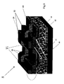
- the transmission conductive layer 21 of the transistor mesh and the spacer 20 serving as gate electrode must be electrically connected and this can easily occur by creating a polysilicon connection bridge 22 as shown in figure 8; in this figure, components and signals common to figures 7 and 6 will maintain the same reference identifiers.
- the speed of the device and the propagation mode of the driving signal will depend on the number of polysilicon connection bridges 22 and on their mutual distance.
- the invention provides the deposition, above the thick oxide 16, of a polysilicon layer 21, suitably doped and of suitable thickness.
- a polysilicon layer 21 suitably doped and of suitable thickness.
- An anisotropic etching follows of the polysilicon 21, suitably masked by means of photolithographic techniques, follows so as to form a spacer of said material which, having filled in the pre-existing cavities, takes the name of recess spacer 20.
- lithographic techniques allows to define both polysilicon paths overhanging the thick dielectric 16 (gate electrode on thick dielectric), and interconnection bridges 22, always in polysilicon, between the overhanging areas of the thick dielectric 16 and the areas with gate oxide, i.e. gate electrode on thin oxide.
- the area below the recess spacer 20 is advantageously used for the formation of the channel.
- the aforesaid polysilicon bridges 22 allow to distribute the signal propagated through the gate electrode on the thick dielectric towards the gate electrode on the thin oxide.
- the peculiarity of the invention consists in the self-alignment between the area of laterally etched thick dielectric 16 and the channel area.
- the process for the realisation of high integration density power MOS devices comprises the following steps:
- This etching step allows to laterally etch the thick dielectric layer 16 with respect to the nitride portions 19 used as hard mask.
- the process must be carried out so as to ensure a high etching selectivity between the thick dielectric layer 16 and the nitride portions 19 used as hard mask.
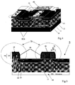
- FIG. 9 An enlarged vertical section view of a layered structure of a high integration density power MOS device realised at the end of the oxide lateral etching step is shown in figure 9, wherein it is evident that the process leads to the formation of a T-like structure with creation of opposite cavities [undercut] under the nitride portions 19.
- the lateral etching step can be realised by means of chemical solutions based on hydrofluoric acid or chemical solutions based on phosphoric acid or with a suitable isotropic etching in dry.
- a lateral etching step can be realised by means of an etching "in wet” with solutions based on hydrofluoric acid HF.
- BOE solutions Bovine Oxide Etcher
- etching speed 950 A/min
- etching unevenness 5%. This allows to control well the recession of the thick dielectric layer 16 with respect to the overhanging nitride portions 19, given that the nitride is not etched in solutions based on HF.
- the process provides further steps of:
- Figure 10 shows an image obtained by means of scanning electron microscopy [Scanning Electron Microscope] (SEM), of a layered structure of a power MOS device after the lateral etching of the thick dielectric layer 16 and the polysilicon 24 deposition.
- SEM scanning electron microscopy
- the self-alignment of the spacer 20 serving as gate electrode and especially the self-alignment of the body 12 and source 13 diffusions make the photolithography definition realising the initial thick dielectric structure less critical.
- the formation of the recess spacer 20 serving as gate electrode occurs in a process carried out without masking.
- the formation of the recess spacer 20 serving as gate electrode occurs in a process with masking.
- the method further provides the steps of:
- the process is carried out by means of an etching in plasma.
- an etching in plasma By exploiting the high anisotropy it is possible to define, in a simultaneous way, the spacer 20 serving as gate electrode, in correspondence with the step created by the laterally etched thick dielectric layer 16 and the polysilicon transmission conductive layers 21, in the regions masked with the resist 23.
- the spacer 20 serving as gate electrode, in correspondence with the step created by the laterally etched thick dielectric layer 16 and the polysilicon transmission conductive layers 21, in the regions masked with the resist 23.
- the nitride portions 19 and the gate oxide thin layer 15 uncovered at the end of the process will be used as stopping layers (and for the endpoint reading).
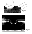
- FIG. 12 An enlarged vertical section view of a layered structure of a power MOS device, further to the anisotropic etching step described is shown in figure 12.
- the corresponding polysilicon recess spacer 20 serving as gate electrode can be seen in figure 13, wherein a section is shown obtained by means of scanning electron microscopy (SEM), of a layered structure of a power MOS device, further to the anisotropic etching step described.
- SEM scanning electron microscopy
- An advantage of the process proposed consists in the possibility of converting the polysilicon layer 24 on the thick dielectric into a suitable silicide (only by way of example cobalt silicide) in an almost complete way, without however risking damaging effects of the gate oxide or of mechanical stress.
- the process according to the invention solves the technical problem and it attains several advantages with respect to the prior art; the first of which is that of being compatible with the technologies VLSI.
- the process in fact, does not require particular alignment restrictions between the various masks necessary for the formation of the elementary MOS, avoiding premature breakdown problems.
- the margin L shown in figure 2 of the prior art description is in fact ensured not by an alignment between the two masks but by a deposition and etching process.
- the physical separation between the polysilicon of the transmission conductive layer (21) and the one placed on the gate oxide allows to transform the whole polysilicon thickness into a silicide without problems on the gate oxide (faultiness or mechanical stress).
Landscapes
- Insulated Gate Type Field-Effect Transistor (AREA)
- Electrodes Of Semiconductors (AREA)
- Element Separation (AREA)
Abstract
- providing a doped semiconductor substrate (10) with a first type of conductivity (N);
- forming, on the substrate (10), a semiconductor layer (11) with lower conductivity (N-);
- forming, on the semiconductor layer (11), a dielectric layer (16) of thickness comprised between 3000 and 13000 A (Angstrom);
- depositing, on the dielectric layer (16), a hard mask layer;
- masking the hard mask layer by means of a masking layer;
- etching the hard mask layers and the underlying dielectric layer (16) for defining a plurality of hard mask portions (19) to protect said dielectric layer (16);
- removing the masking layer;
- isotropically and laterally etching said dielectric layer forming lateral cavities in said dielectric layer (16) below said hard mask portions (19);
- forming a gate oxide (15) of thickness comprised between 150 and 1500 A (Angstrom)
- depositing a conductor material (24) in said cavities and above the same to form a recess spacer (20), which is totally aligned with a gate structure (14) comprising said thick dielectric layer (16) and said gate oxide (15).
Description
- The present invention relates to a process for the realisation of a high integration density power MOS device.
- More specifically, the invention relates to a process for the realisation of a high integration density power MOS device comprising the steps of:
- providing a doped semiconductor substrate with a first type of conductivity;
- forming, on the substrate, a semiconductor substrate with lower conductivity;
- forming, on said semiconductor layer, a dielectric layer of thickness comprised between 3000 and 13000 A (Angstrom);
- depositing, on said dielectric layer, a hard mask layer;
- masking the hard mask layer by means of a masking layer;
- etching the hard mask layers and the underlying dielectric layer to define a plurality of hard mask portions to protect said dielectric layer;
- removing the masking layer.
- As it is well known, power MOS devices, especially low voltage ones, have been characterised, especially during the last years, by a continuous increase of the integration density of transistor elementary structures, following a process of dimension reduction, so called "scaling down" typical of integration techniques so called "Very Large-Scale Integration" (VLSI).
- In transistor elementary structures, this has implied the use of thinner and thinner gate oxides, less and less deep junctions and more and more reduced channel lengths. Power MOS devices formed by completely submicrometric transistor elementary structures are, nowadays, a reality present on the market.
- This technological development proceeds from the application need of having smaller and smaller output resistances from transistor elementary structures and higher and higher switch speeds.
- The need is added of driving power MOS devices, with lower and lower gate voltages, so as to allow the corresponding driving circuits [driver] a low voltage output (1.8-2.5 Volt).
- From the technological viewpoint the previously exposed necessities result in the need of suitably designing the transistor elementary structure, whose repetition will constitute the power MOS device. In particular, the gate dielectric thickness, typically silicon oxide, is more and more reduced so as to obtain threshold voltage values lower than the Volt without deteriorating the breakdown characteristics of the MOS device due to a possible punch through effect of the channel whose length is more and more reduced.
- However, this implies remarkable drawbacks.
- For example, in terms of switch speed, the reduction of the gate dielectric thickness, together with the higher integration density, implies an increase of the MOS device capacities and thus a slowdown in the switch.
- Moreover, the switch speed does not exclusively depend on the capacity but also on the resistance seen from the driver for loading and unloading the capacitive elements of the power MOS device. Such resistance takes the name of inner gate resistance and it depends on the physical and geometrical characteristics of the group of all the elementary structures.
- In particular, figure 1 schematically shows an equivalent electric circuit 1 of n elementary MOS transistors Ti (i=1..n) in parallel, which constitute a power MOS device. Such elementary transistors have a common control terminal Gate and common conduction terminals Drain and Source. This circuit also shows a gate biasing network wherein the resistive contribution brought by inner resistances Ri (i=1..n) of the n elementary MOS transistors Ti constituting the power MOS device is highlighted.
- All in all, for improving the dynamic performances of a power MOS device, as the one shown for example in figure 1, it is necessary to reduce to the minimum not only the total gate capacity but also the resistance thereof, determined by the contribution of the resistances Ri, so as to reduce the time constant (RC), given by the product between the total gate resistance by the device capacity.
- So far the known technique has been oriented on technological and circuit innovation paths to separately solve the problems correlated to the minimisation of the gate capacity and resistance of a power MOS device.
- A first known solution, turned towards minimising the capacity, consists in integrating, in MOS technologies, gate dielectrics different from thermal SiO2 such as for example, hafnium oxide, aluminium oxide, multilayers of silicon oxide/silicon nitride, etc.
- However, the activities linked to the adoption of alternative materials are long and subject to tests which could require prohibitive times for the current market of the devices at issue, making a solution to the highlighted problem not attainable.
- A second known solution, turned towards minimising the capacity, by increasing the switch speed of the device, provides a change of the geometry of the single transistor elementary structure of the power MOS device. In particular, this structure is changed in the gate dielectric in active area, which is realised with two layers having different thickness:
- a first relatively thin layer is realised on the source channel, so as to make a driving of the low threshold voltage MOS device possible;
- another layer of greater thickness is realised so that it is extended to the sole region of the gate/drain capacitor (intercell), so as to remarkably reduce the transition capacity of the MOS device.
- A technique for realising power VDMOS devices with vertical diffusion, both with channel n, and with channel p, and with double gate oxide thickness in active area, is described in the US patents N° 6,222,232 and N° 6,326,271 and the resulting structure is shown in figure 2, globally indicated with 2 and wherein source, body and drain regions are respectively indicated with 13, 12 and 11.
- In this technique, the definition procedure of the gate electrode mainly requires a thermal growth of a silicon oxide thick film OX, its photolithographic definition in active area regions, the successive growth of a thin gate oxide film OXG which will surmount a channel ch. The deposition of a gate poly electrode (doped polysilicon or polysilicon stack / metallic silicide) and the definition of the gate geometries through suitable phototechnique maskings then follow.
- The rest of the process is that typical of a vertical diffusion power MOS, with realisation of a channel through lateral diffusion of a well (of the p type in a channel n device and of the n type in the device of opposite polarity), and of a small heavily doped source well, opening through phototechnique of source and gate contacts, and front and rear metallisation of the so called "semiconductor slice", which substantially represents the substrate whereon the MOS is integrated.
- Unfortunately, the prior art for the realisation of a gate with double oxide thickness, of a transistor elementary structure of power MOS devices, clashes on the growing need of increasing the integration density however safeguarding the alignment of the planar structures in active area. In fact, the prior art provides the use of a photolithography to define the thick oxide region OX in the transistor elementary structure and of a successive and more delicate photolithography step for the definition of the gate poly electrode geometry.
- The need of having a symmetrical and uniform diffused channel imposes, in this case, a great margin between the delimitation of the gate electrode, whose projection is indicated with A in figure 2, and the edge of the structure in central thick oxide OX, whose projection is indicated with B in figure 2.
- A margin indicated with L in figure 2 must be sufficiently wide as to ensure that possible maximum misalignments in the lithographic definition of the gate poly electrode do not determine a channel extension Lch under the thick oxide OX however in an asymmetrical way.
- Obviously, the presence of this margin reduces the integration density of the device on semiconductor.
- In the prior art there exist "self-aligning" methods able to reduce the above margin L and based on the formation of spacers realised at the edges of the thick oxide, as well highlighted in figure 3, wherein source, body and drain regions will be indicated as in figure 2. Figure 3 shows a
structure 3 with double self-aligning gate thickness of power VDMOS devices. This structure has two VDMOS devices, indicated with T1 and T2, having a first gate dielectric thickness, indicated respectively with OXG1 and OXG2 and a second gate dielectric thickness, indicated respectively with OX1 and OX2. - Opposite spacers SP delimit an opening IN, through which the plants for the formation of body wells are realised, from the start of the thick oxide OX1 and OX2. A margin LI, comprised between the projection BI of an end of the opening IN through which the plants for the formation of body wells are realised and the projection AI of the end of the thick oxide OX1 nearer to the opening IN, is lower than the margin D1 shown in fig.2.
- Unfortunately, also these self-aligning methods of the known type have serious drawbacks; being based on anisotropic etchings, they tie the margin LI between the openings through which the plants for the formation of body wells are realised and the start of the thick oxide, to the thickness of the polysilicon or dielectric layers used for their realisation.
- The thickness of these layers being normally lower than the micrometre it follows that also this margin LI, and, in particular, the channel length LI ch, will be lower than the micrometre. If on one side this represents an advantage for the submicrometric structures used in low voltage applications, this fact represents a limit for the technologies destined to high voltage applications since channel lengths LI ch lower than the micrometre can trigger premature breakdown problems.
- Other techniques being known in the literature, for example as described in the US patent no. 5,933,734, are orientated on technological and circuit innovation paths, to solve the problems correlated with the minimisation of the gate resistance of a power MOS device. The structure is realised with the technique described in the cited patent is shown in figure 4, wherein source, body and drain regions will be indicated as in figures 2 and 3, also overlapped onto a
substrate 10. Therein, a gate mesh comprising gate electrodes EGi (i=1..n) is realised with a suitably doped polysilicon pls layer placed in parallel to a metal or metallic silicide slc, at a lower resistivity with respect to the polysilicon. - The technical problem underlying the present invention is that of defining a process for realising a high integration density power MOS device, with gate electrode having double oxide thickness, having such structural characteristics as to be used also in technologies with scale dimensions VLSI, but with channel dimensions being not necessarily submicrometric, overcoming the limits and/or the drawbacks of the embodiments proposed by the prior art.
- The solution idea underlying the present invention is that of realising a high integration density power device with structure having double gate thickness, the structure being totally self-aligned with the gate electrode.
- On the basis of this solution idea the technical problem is solved by a process for the realisation of a high integration density power MOS device as previously indicated and defined by the characterising part of claim 1.
- The problem is also solved by a power device defined by the characterising part of
claim 5. - The characteristics and the advantages of the process according to the invention will be apparent from the following description of an embodiment thereof given by way of indicative and non limiting example with reference to the annexed drawings.
- In these drawings:
- figure 1 schematically shows an equivalent electric circuit of a power MOS device according to the prior art;
- figure 2 shows an enlarged vertical section view of a first layered structure of a power MOS device according to the prior art;
- figure 3 shows an enlarged vertical section view of a second layered structure of a power MOS device according to the prior art;
- figure 4 shows an enlarged perspective view of a third layered structure of a power MOS device according to the prior art;
- figure 5 shows an enlarged vertical section view of a layered structure of a power MOS device in a first embodiment of the present invention.
- figure 6 shows an enlarged vertical section view of a layered structure of a power MOS device in a second embodiment of the present invention.
- figure 7 shows an enlarged perspective view of the structure of figure 6.
- figure 8 shows an enlarged perspective view of an evolution of the structure of figure 6;
- figure 9 shows an enlarged vertical section view of a layered structure of a power MOS device in a step of the process for realising the device according to the present invention.
- figure 10 shows an image obtained through scanning electronic microscopy [Scanning Electron Microscope] (SEM) of a layered structure of a power MOS device, in a step successive to that of figure 9 of the process for realising the device according to the present invention.
- figure 11 shows an enlarged vertical section view of a layered structure of a power MOS device in another step of the process for realising the device according to the present invention;
- figure 12 shows an enlarged vertical section view of a layered structure of a power MOS device in a further step of the process for realising the device according to the present invention;
- figure 13 shows a section obtained through scanning electron microscopy (SEM), of a layered structure of a power MOS device in the step of the process for realising the device shown in figure 12 according to the present invention;
- With reference to these figures, and in particular to the example of Figure 5, an enlarged vertical section view is shown of a high integration density power MOS device, comprising transistor elementary structures, according to a first embodiment of the present invention, is globally and schematically indicated with 5.
- The
power device 5 essentially comprises a heavily doped semiconductor substrate of the N type (N+) to ensure the conduction and resistance characteristics in voltage of the desired power device. - On this substrate a second doped semiconductor layer of the N type is grown (N-) with lower conductivity with respect to the first layer.
- As it has been seen in relation with the prior art, in particular with reference to figures 2 and 3, the
conductor layer 11 serves as drain region of thepower device 5; transistor elementary structures Ti (i=1..n) comprise abody region 12 within which the source well 13 is realised and completely confined. - Suitably, the transistor elementary structures Ti (i=1..n) have
gate structures 14 of the type with double thickness, which comprise a first gate oxidethin layer 15, above which adielectric layer 16 is centrally present having greater thickness with respect to thefirst layer 15. This layer of greater thickness defines acentral portion 17 delimited bypolysilicon lateral portions 18. - A so called conductor polysilicon mesh realises the connection of all the elementary transistors Ti to define the high integration density
power MOS device 5, as schematically shown in the prior art description, with reference to figure 1. - Suitably, but without this representing a limit for the Applicant's rights, the
central portion 17 of thick dielectric is realised with a thermally grown silicon oxide; alternatively, it can be realised with a sequence of suitable layers such as, for example, multilayers of SixOy/SiwNz or SixOyNz. - Advantageously according to the invention the
gate structure 14 further comprises anupper nitride portion 19, arranged above the thick dielectriccentral portion 17 of the transistor mesh and of thepolysilicon lateral portions 18; thisnitride portion 19 insulates the entire upper base surface of theabove portions - Advantageously according to the invention the
gate structure 14, surmounted by thenitride portion 19, is flanked by twospacers 20 of conductive material, arranged so as to cover, with their own base, the opposite ends of the upper surface of the firstthin layer 15 of gate oxide, left free since not overlapped neither by the thick dielectriccentral portion 17 of the transistor mesh nor by thelateral polysilicon portions 18. - Advantageously according to the invention the two
spacers 20 of conductive material serve as gate electrode. Suitably, but without this representing a limit for the Applicant's rights, theabove spacers 20 are realised with suitably doped polysilicon; alternatively, they can be realised with metal. - Advantageously according to the invention the presence of the two
spacers 20 allows a self-alignment of thegate structure 14 and of thebody 12 andsource 13 regions, facilitating the definition of the photolithography which realises the initial thick dielectric structure, as it will be shown in detail in the description of the process for realising the high integration density power MOS device. - Advantageously, with reference to figures 6 and 7 which show a high integration density power MOS device comprising transistor elementary structures Ti it can be realised by separating the
gate structure 14 from a transmissionconductive layer 21 of the transistor mesh, by means of thenitride portion 19 according to a second embodiment of the present invention. - Such a device is shown in a section and perspective view, respectively in figures 6 and 7, globally and schematically indicated with 7. In both figures, components common to figure 5 will be described with the same reference identifiers.
- Advantageously according to the invention a transmission
conductive layer 21 displays, in this case, the sole function of transmission line, i.e. it distributes the biasing signal to the elementary structures Ti composing the high integration density power MOS device. - Suitably, without this representing a limit for the Applicant's rights, this transmission
conductive layer 21 is realised in polysilicon. - Advantageously, according to the invention, the transmission
conductive layer 21, placed above adielectric layer 16 being much thicker than the gate oxide, can be made very conductive both by hyper-doping and entirely transforming it into a metallic layer, without jeopardising the faultiness of thespacer 20 serving as gate electrode. - The transmission
conductive layer 21, in particular, can be realised with a silicide layer occupying the whole thickness of the initial polysilicon either with a metallic layer overlapped onto the polysilicon layer or with a completely metallic layer. - Suitably, the transmission
conductive layer 21 of the transistor mesh and thespacer 20 serving as gate electrode must be electrically connected and this can easily occur by creating apolysilicon connection bridge 22 as shown in figure 8; in this figure, components and signals common to figures 7 and 6 will maintain the same reference identifiers. - The speed of the device and the propagation mode of the driving signal will depend on the number of polysilicon connection bridges 22 and on their mutual distance.
- Summarising, the invention provides the deposition, above the
thick oxide 16, of apolysilicon layer 21, suitably doped and of suitable thickness. By exploiting the high conformability of said polysilicon layer, the cavities left from the preceding dielectric lateral etching are filled in. - An anisotropic etching follows of the
polysilicon 21, suitably masked by means of photolithographic techniques, follows so as to form a spacer of said material which, having filled in the pre-existing cavities, takes the name ofrecess spacer 20. - Simultaneously, the use of lithographic techniques allows to define both polysilicon paths overhanging the thick dielectric 16 (gate electrode on thick dielectric), and
interconnection bridges 22, always in polysilicon, between the overhanging areas of thethick dielectric 16 and the areas with gate oxide, i.e. gate electrode on thin oxide. - The area below the
recess spacer 20 is advantageously used for the formation of the channel. - The aforesaid polysilicon bridges 22 allow to distribute the signal propagated through the gate electrode on the thick dielectric towards the gate electrode on the thin oxide.
- The peculiarity of the invention consists in the self-alignment between the area of laterally etched
thick dielectric 16 and the channel area. - The process will be now described for the realisation of the high integration density
power MOS devices - The process steps and the structures described hereafter do not form a complete process flow for the realisation of high integration density power MOS devices. In fact, the present invention can be put into practice together with the techniques for realising MOS devices currently used in the field and hereafter only the process steps necessary for the comprehension of the invention are described.
- According to the two embodiments of the present invention, the process for the realisation of high integration density power MOS devices comprises the following steps:
- providing a doped
semiconductor substrate 10 of the N type and with high conductivity and subsequently growing a further dopedsemiconductor layer 11 of the N type, with lower conductivity (N-); - forming a
thick dielectric layer 16 of thickness comprised for example between 3000 and 13000 A (Angstrom);
Suitably, but not limitatively, this dielectric ofgreater thickness 16 is realised with thermally grown silicon oxide; alternatively, it can be realised with a sequence of suitable layers such as, for example, multilayers of SixOy/SiwNz or SixOyNz. - depositing, above the thick dielectric layer 16 a so called hard mask of thickness comprised between 150 and 1000 A (Angstrom);
Suitably, but not limitatively, this hard mask is realised with a silicon nitride layer; alternatively, it can be realised with polysilicon; - providing a masking, by positioning a resist layer, of the nitride layer to define a plurality of
nitride portions 19 to protect the underlyingthick dielectric layer 16; - etching in an anisotropic way (i.e. dry etching) the nitride layer and the underlying
thick dielectric 16; - removing the resist;
- etching, laterally and in an anisotropic way, the
thick dielectric layer 16 for a lateral thickness comprised between 2000 and 6000 A (Angstrom). - This etching step allows to laterally etch the
thick dielectric layer 16 with respect to thenitride portions 19 used as hard mask. The process must be carried out so as to ensure a high etching selectivity between thethick dielectric layer 16 and thenitride portions 19 used as hard mask. - An enlarged vertical section view of a layered structure of a high integration density power MOS device realised at the end of the oxide lateral etching step is shown in figure 9, wherein it is evident that the process leads to the formation of a T-like structure with creation of opposite cavities [undercut] under the
nitride portions 19. - Suitably, the lateral etching step can be realised by means of chemical solutions based on hydrofluoric acid or chemical solutions based on phosphoric acid or with a suitable isotropic etching in dry.
- By way of example, a lateral etching step can be realised by means of an etching "in wet" with solutions based on hydrofluoric acid HF. By using for example BOE solutions (Buffered Oxide Etcher) with HF and NH4F in proportion 1 to 7 (HF:NH4F =1:7) at 28°C, there is an etching speed of 950 A/min and an etching unevenness of 5%. This allows to control well the recession of the
thick dielectric layer 16 with respect to the overhangingnitride portions 19, given that the nitride is not etched in solutions based on HF. - The process provides further steps of:
- thermally growing a
gate oxide 15 of thickness comprised between 150 and 1500 A (Angstrom); - depositing
conductive material 24, in particular polysilicon in the cavities realised below thenitride portions 19 and above the same, with formation of arecess spacer 20, suitable to allow the total alignment between the structure with double gate thickness and the gate electrode.
Hereafter in the description, reference will be made, not limitatively, topolysilicon 24, this meaning, more in general, a conductive material; subsequently a - possible doping of the deposited
polysilicon 24 can be provided. - Figure 10 shows an image obtained by means of scanning electron microscopy [Scanning Electron Microscope] (SEM), of a layered structure of a power MOS device after the lateral etching of the
thick dielectric layer 16 and thepolysilicon 24 deposition. - Advantageously according to the invention of the self-alignment of the
spacer 20 serving as gate electrode and especially the self-alignment of thebody 12 andsource 13 diffusions make the photolithography definition realising the initial thick dielectric structure less critical. - In the first embodiment of the present invention described up to now the formation of the
recess spacer 20 serving as gate electrode, occurs in a process carried out without masking. In a second embodiment, the formation of therecess spacer 20 serving as gate electrode occurs in a process with masking. - In consequence, on the basis of the second embodiment of the present invention, the method further provides the steps of:
- providing a masking, by positioning a resist
layer 23, of the regions which will lead to the formation of the transmission conductive layers 21.
A section view of a layered structure of a power MOS device, further to the photomasking step described, is shown in figure 11. - anisotropic etching of the polysilicon 24 (masked spacer) and removal of the resist 23.
- Suitably the process is carried out by means of an etching in plasma. By exploiting the high anisotropy it is possible to define, in a simultaneous way, the
spacer 20 serving as gate electrode, in correspondence with the step created by the laterally etchedthick dielectric layer 16 and the polysilicon transmissionconductive layers 21, in the regions masked with the resist 23. For the etching process in plasma both thenitride portions 19 and the gate oxidethin layer 15 uncovered at the end of the process will be used as stopping layers (and for the endpoint reading). - An enlarged vertical section view of a layered structure of a power MOS device, further to the anisotropic etching step described is shown in figure 12.
- The corresponding
polysilicon recess spacer 20 serving as gate electrode can be seen in figure 13, wherein a section is shown obtained by means of scanning electron microscopy (SEM), of a layered structure of a power MOS device, further to the anisotropic etching step described. - An advantage of the process proposed consists in the possibility of converting the
polysilicon layer 24 on the thick dielectric into a suitable silicide (only by way of example cobalt silicide) in an almost complete way, without however risking damaging effects of the gate oxide or of mechanical stress. - The presence of a photolithographic operation dedicated to the realisation of the transmission conductive layer (21) allows to add or even substitute the
polysilicon 24 used with a metal (double metal structure) with enormous advantages on the device gate resistance. - Allowing to reduce the gate resistance, the process described can be applied to processes known in the literature, such as for example the one shown in the US patent No. 5,933,734 wherein a gate mesh realised with a suitably doped polysilicon layer is placed in parallel to a layer with a lower resistivity (metal or a metallic silicide, such as cobalt silicide).
- Only by way of example, the formation of the cobalt silicide can be realised by means of the following process steps according to the prior art:
- deposition of a deposited oxide layer (for example TEOS)
- masking process allowing to protect with resist the regions wherein the silicide will not have to be formed
- dry etching process to eliminate the TEOS layer from the regions wherein the formation of a cobalt silicide layer and successive removal of the resist will occur
- deposition of metallic cobalt by means of a sputtering process;
- sintering processes for the formation of the silicide.
- The process according to the invention solves the technical problem and it attains several advantages with respect to the prior art; the first of which is that of being compatible with the technologies VLSI.
- The process, in fact, does not require particular alignment restrictions between the various masks necessary for the formation of the elementary MOS, avoiding premature breakdown problems. The margin L shown in figure 2 of the prior art description is in fact ensured not by an alignment between the two masks but by a deposition and etching process.
- The physical separation between the polysilicon of the transmission conductive layer (21) and the one placed on the gate oxide allows to transform the whole polysilicon thickness into a silicide without problems on the gate oxide (faultiness or mechanical stress).
- The presence of a photolithographic operation dedicated to the realisation of the transmission conductive layer (21) of a transistor mesh allows to add or even substitute the polysilicon used with a metal (double metal structure) with enormous advantages on the device gate resistance.
Claims (17)
- Process for the realisation of a high integration density power MOS device comprising the steps of:providing a doped semiconductor substrate (10) with a first type of conductivity (N);forming, on the substrate (10), a semiconductor layer (11) with lower conductivity (N-);forming, on said semiconductor layer (11), a dielectric layer (16) of thickness comprised between 3000 and 13000 A (Angstrom);depositing, on said dielectric layer (16), a hard mask layer;masking the hard mask layer by means of a masking layer;etching the hard mask layers and the underlying dielectric layer (16) for defining a plurality of hard mask portions (19) to protect said dielectric layer (16);removing the masking layer;characterised in:isotropically and laterally etching said dielectric layer forming lateral cavities in said dielectric layer (16) below said hard mask portions (19);forming a gate oxide (15) of thickness comprised between 150 and 1500 A (Angstrom)depositing a conductor material (24) in said cavities and above the same to form a recess spacer (20), which is totally aligned with a gate structure (14) comprising said thick dielectric layer (16) and said gate oxide (15).
- Process according to claim 1 wherein said recess spacer (20) serves as gate electrode.
- Process according to claim 1 characterised in that it further comprises the steps of:providing a masking, by positioning a resist layer (23), of the regions which will lead signal transmission conductive layers (21), above said thick dielectric layer (16);anisotropically etching the conductor layer (24) and removing said resist layer (23).
- Process according to claim 1, wherein said conductor material (24) is suitably doped polysilicon.
- Process according to claim 1 wherein the anisotrpic etching is carried out by means of an etching in plasma.
- Process according to claim 1 wherein the hard mask is made of silicon nitride.
- Process according to claim 1 wherein the hard mask is made of polysilicon.
- High integration density power MOS device comprising a substrate (10) of a doped semiconductor with a first type of conductivity (N) whereon a semiconductor layer (11) with lower conductivity (N-) is formed, transistor elementary structures Ti (i=1..n) comprising body regions (12), arranged above in said semiconductor (11) inside which the source regions (13) are confined, characterised in that it comprises in each of said transistor elementary structures Ti (i=1..n) a gate structure (14) of the type with double thickness comprising a first thin layer (15) of gate oxide onto which, at least partially, a dielectric layer (17) is overlapped having thickness greater than said first layer (15) and laterally delimited by lateral portions (18) of conductive material, said gate structure (14) further comprising a nitride upper portion (19) above the thick dielectric layer (17) and said lateral portions (18) of conductor material.
- Power MOS device, according to claim 8, characterised in that it comprises opposite spacers (20) of the same conductor material (18) aligned with said gate structure (14) and with said body (12) and source (13) regions.
- Power MOS device according to claim 9 wherein said spacer (20) serves as gate electrode.
- Power MOS device according to claim 9 wherein said gate structure (14) is separated, by means of said nitride portion (19), from a transmission conductive layer (21) of a transistors mesh.
- Power MOS device according to claim 11, wherein said transmission conductive layer (21) is realised in polysilicon.
- Power MOS device according to claim 11, wherein said signal transmission conductive layer (21) is realised with a silicide layer.
- Power MOS device according to claim 11, wherein a metallic layer is overlapped onto said signal transmission conductive layer (21).
- Power MOS device according to claim 11, wherein said signal transmission conductive layer (21) is realised with a completely metallic layer.
- Power MOS device according to claim 11, wherein said gate structure (14), distribute a biasing signal to transistor elementary structures (Ti), by means of said signal transmission conductive layer (21).
- Power MOS device according to all the preceding claims, wherein the substrate (10) and/or the overhanging substrate (11), are realised by means of doped semiconductors of the P type according to the necessary conductivity.
Priority Applications (1)
| Application Number | Priority Date | Filing Date | Title |
|---|---|---|---|
| EP10011934A EP2302684A3 (en) | 2004-11-19 | 2005-11-18 | Power MOS device |
Applications Claiming Priority (1)
| Application Number | Priority Date | Filing Date | Title |
|---|---|---|---|
| IT002243A ITMI20042243A1 (en) | 2004-11-19 | 2004-11-19 | PROCESS FOR THE REALIZATION OF A HIGH DENSITY MOS INTENSION POWER DEVICE |
Related Child Applications (1)
| Application Number | Title | Priority Date | Filing Date |
|---|---|---|---|
| EP10011934.6 Division-Into | 2010-09-30 |
Publications (3)
| Publication Number | Publication Date |
|---|---|
| EP1659637A2 true EP1659637A2 (en) | 2006-05-24 |
| EP1659637A3 EP1659637A3 (en) | 2006-07-19 |
| EP1659637B1 EP1659637B1 (en) | 2011-01-12 |
Family
ID=36088155
Family Applications (2)
| Application Number | Title | Priority Date | Filing Date |
|---|---|---|---|
| EP05025287A Expired - Lifetime EP1659637B1 (en) | 2004-11-19 | 2005-11-18 | Method of manufacturing a power MOS device |
| EP10011934A Withdrawn EP2302684A3 (en) | 2004-11-19 | 2005-11-18 | Power MOS device |
Family Applications After (1)
| Application Number | Title | Priority Date | Filing Date |
|---|---|---|---|
| EP10011934A Withdrawn EP2302684A3 (en) | 2004-11-19 | 2005-11-18 | Power MOS device |
Country Status (4)
| Country | Link |
|---|---|
| US (2) | US7601610B2 (en) |
| EP (2) | EP1659637B1 (en) |
| DE (1) | DE602005025845D1 (en) |
| IT (1) | ITMI20042243A1 (en) |
Families Citing this family (7)
| Publication number | Priority date | Publication date | Assignee | Title |
|---|---|---|---|---|
| US9178054B2 (en) | 2013-12-09 | 2015-11-03 | Micrel, Inc. | Planar vertical DMOS transistor with reduced gate charge |
| US9184278B2 (en) * | 2013-12-09 | 2015-11-10 | Micrel, Inc. | Planar vertical DMOS transistor with a conductive spacer structure as gate |
| US9607635B1 (en) * | 2016-04-22 | 2017-03-28 | International Business Machines Corporation | Current perpendicular-to-plane sensors having hard spacers |
| US9947348B1 (en) | 2017-02-28 | 2018-04-17 | International Business Machines Corporation | Tunnel magnetoresistive sensor having leads supporting three-dimensional current flow |
| US10803889B2 (en) | 2019-02-21 | 2020-10-13 | International Business Machines Corporation | Apparatus with data reader sensors more recessed than servo reader sensor |
| US11074930B1 (en) | 2020-05-11 | 2021-07-27 | International Business Machines Corporation | Read transducer structure having an embedded wear layer between thin and thick shield portions |
| US11114117B1 (en) | 2020-05-20 | 2021-09-07 | International Business Machines Corporation | Process for manufacturing magnetic head having a servo read transducer structure with dielectric gap liner and a data read transducer structure with an embedded wear layer between thin and thick shield portions |
Family Cites Families (27)
| Publication number | Priority date | Publication date | Assignee | Title |
|---|---|---|---|---|
| US4055884A (en) * | 1976-12-13 | 1977-11-01 | International Business Machines Corporation | Fabrication of power field effect transistors and the resulting structures |
| US4318759A (en) * | 1980-07-21 | 1982-03-09 | Data General Corporation | Retro-etch process for integrated circuits |
| US4748103A (en) * | 1986-03-21 | 1988-05-31 | Advanced Power Technology | Mask-surrogate semiconductor process employing dopant protective region |
| EP0518418A1 (en) * | 1991-06-10 | 1992-12-16 | Koninklijke Philips Electronics N.V. | Method of manufacturing a semiconductor device whereby field oxide regions are formed in a surface of a silicon body through oxidation |
| US5430314A (en) * | 1992-04-23 | 1995-07-04 | Siliconix Incorporated | Power device with buffered gate shield region |
| DE69434268T2 (en) | 1994-07-14 | 2006-01-12 | Stmicroelectronics S.R.L., Agrate Brianza | Integrated structure of a high-speed MOS technologist power device and related manufacturing method |
| US5795793A (en) * | 1994-09-01 | 1998-08-18 | International Rectifier Corporation | Process for manufacture of MOS gated device with reduced mask count |
| US5510281A (en) * | 1995-03-20 | 1996-04-23 | General Electric Company | Method of fabricating a self-aligned DMOS transistor device using SiC and spacers |
| JP3166148B2 (en) | 1995-07-11 | 2001-05-14 | 横河電機株式会社 | Semiconductor device |
| DE69534919T2 (en) * | 1995-10-30 | 2007-01-25 | Stmicroelectronics S.R.L., Agrate Brianza | Power device in MOS technology with a single critical size |
| EP0817274B1 (en) | 1996-07-05 | 2004-02-11 | STMicroelectronics S.r.l. | Asymmetric MOS technology power device |
| US6025230A (en) * | 1997-11-06 | 2000-02-15 | Mageposer Semiconductor Corporation | High speed MOSFET power device with enhanced ruggedness fabricated by simplified processes |
| US6187694B1 (en) * | 1997-11-10 | 2001-02-13 | Intel Corporation | Method of fabricating a feature in an integrated circuit using two edge definition layers and a spacer |
| GB9726829D0 (en) | 1997-12-19 | 1998-02-18 | Philips Electronics Nv | Power semiconductor devices |
| US6107649A (en) * | 1998-06-10 | 2000-08-22 | Rutgers, The State University | Field-controlled high-power semiconductor devices |
| US6215152B1 (en) * | 1998-08-05 | 2001-04-10 | Cree, Inc. | MOSFET having self-aligned gate and buried shield and method of making same |
| KR20000051294A (en) * | 1999-01-20 | 2000-08-16 | 김덕중 | DMOS field effect transistor with improved electrical characteristics and fabricating method thereof |
| JP4917709B2 (en) * | 2000-03-06 | 2012-04-18 | ローム株式会社 | Semiconductor device |
| US6710405B2 (en) * | 2001-01-17 | 2004-03-23 | Ixys Corporation | Non-uniform power semiconductor device |
| US6756644B2 (en) * | 2001-03-28 | 2004-06-29 | International Rectifier Corporation | Ultra low QGD power MOSFET |
| DE10131917A1 (en) * | 2001-07-02 | 2003-01-23 | Infineon Technologies Ag | Method for producing a step-like structure on a substrate |
| US6706591B1 (en) * | 2002-01-22 | 2004-03-16 | Taiwan Semiconductor Manufacturing Company | Method of forming a stacked capacitor structure with increased surface area for a DRAM device |
| US7045845B2 (en) * | 2002-08-16 | 2006-05-16 | Semiconductor Components Industries, L.L.C. | Self-aligned vertical gate semiconductor device |
| US6979863B2 (en) * | 2003-04-24 | 2005-12-27 | Cree, Inc. | Silicon carbide MOSFETs with integrated antiparallel junction barrier Schottky free wheeling diodes and methods of fabricating the same |
| JP4179147B2 (en) * | 2003-11-28 | 2008-11-12 | 株式会社デンソー | Silicon carbide semiconductor device |
| US7105410B2 (en) * | 2004-04-09 | 2006-09-12 | Analog And Power Electronics Corp. | Contact process and structure for a semiconductor device |
| US20060086974A1 (en) * | 2004-10-26 | 2006-04-27 | Power Integrations, Inc. | Integrated circuit with multi-length power transistor segments |
-
2004
- 2004-11-19 IT IT002243A patent/ITMI20042243A1/en unknown
-
2005
- 2005-11-18 EP EP05025287A patent/EP1659637B1/en not_active Expired - Lifetime
- 2005-11-18 EP EP10011934A patent/EP2302684A3/en not_active Withdrawn
- 2005-11-18 DE DE602005025845T patent/DE602005025845D1/en not_active Expired - Lifetime
- 2005-11-21 US US11/285,742 patent/US7601610B2/en not_active Expired - Fee Related
-
2009
- 2009-09-01 US US12/551,999 patent/US8013384B2/en not_active Expired - Fee Related
Non-Patent Citations (1)
| Title |
|---|
| None |
Also Published As
| Publication number | Publication date |
|---|---|
| EP1659637B1 (en) | 2011-01-12 |
| US7601610B2 (en) | 2009-10-13 |
| EP2302684A2 (en) | 2011-03-30 |
| US20060138537A1 (en) | 2006-06-29 |
| ITMI20042243A1 (en) | 2005-02-19 |
| EP2302684A3 (en) | 2012-03-14 |
| DE602005025845D1 (en) | 2011-02-24 |
| US8013384B2 (en) | 2011-09-06 |
| EP1659637A3 (en) | 2006-07-19 |
| US20090321826A1 (en) | 2009-12-31 |
Similar Documents
| Publication | Publication Date | Title |
|---|---|---|
| US11075297B2 (en) | Semiconductor device and method of manufacturing semiconductor device | |
| CN100481503C (en) | Trench gate transistor and fabrication thereof | |
| US7176137B2 (en) | Method for multiple spacer width control | |
| US6953726B2 (en) | High-density split-gate FinFET | |
| KR100511045B1 (en) | Integration method of a semiconductor device having a recessed gate electrode | |
| CN102130015B (en) | Grate-etching process for high voltage field effect transistor | |
| KR100471189B1 (en) | Field effect transistors having a vertical channel and methods of fabricating the same | |
| US6469345B2 (en) | Semiconductor device and method for manufacturing the same | |
| KR101560012B1 (en) | Systems and devices including fin transistors and methods of using, making, and operating the same | |
| JP4851080B2 (en) | LDMOS transistor device, integrated circuit and manufacturing method thereof | |
| US9543298B1 (en) | Single diffusion break structure and cuts later method of making | |
| US8013384B2 (en) | Method for manufacturing a high integration density power MOS device | |
| US9536991B1 (en) | Single diffusion break structure | |
| US6225175B1 (en) | Process for defining ultra-thin geometries | |
| CN1502127A (en) | Semiconductor devices and their formation processes | |
| US20010034109A1 (en) | Trench seimconductor devices reduced trench pitch | |
| EP1535344B1 (en) | Vertical gate semiconductor device with a self-aligned structure | |
| CN103258741A (en) | Nanowire field effect transistor and forming method thereof | |
| KR100956558B1 (en) | Narrow Trench Formation Method and Trench Moosfett Formation Method in Semiconductor Substrate | |
| US20150287782A1 (en) | Integrated circuits and methods of fabrication thereof | |
| US7011929B2 (en) | Method for forming multiple spacer widths | |
| TWI277153B (en) | Semiconductor device with recessed channel and method of fabricating the same | |
| KR20050001193A (en) | Ultra short channel field effect transistor and method for fabricating the same | |
| KR20100069954A (en) | Method of forming a small pattern and method of manufacturing a transistor using the same | |
| CN121548077A (en) | A vertical channel transistor structure and its fabrication method |
Legal Events
| Date | Code | Title | Description |
|---|---|---|---|
| PUAI | Public reference made under article 153(3) epc to a published international application that has entered the european phase |
Free format text: ORIGINAL CODE: 0009012 |
|
| AK | Designated contracting states |
Kind code of ref document: A2 Designated state(s): AT BE BG CH CY CZ DE DK EE ES FI FR GB GR HU IE IS IT LI LT LU LV MC NL PL PT RO SE SI SK TR |
|
| AX | Request for extension of the european patent |
Extension state: AL BA HR MK YU |
|
| PUAL | Search report despatched |
Free format text: ORIGINAL CODE: 0009013 |
|
| AK | Designated contracting states |
Kind code of ref document: A3 Designated state(s): AT BE BG CH CY CZ DE DK EE ES FI FR GB GR HU IE IS IT LI LT LU LV MC NL PL PT RO SE SI SK TR |
|
| AX | Request for extension of the european patent |
Extension state: AL BA HR MK YU |
|
| 17P | Request for examination filed |
Effective date: 20070117 |
|
| 17Q | First examination report despatched |
Effective date: 20070215 |
|
| AKX | Designation fees paid |
Designated state(s): DE FR GB IT |
|
| RAP1 | Party data changed (applicant data changed or rights of an application transferred) |
Owner name: STMICROELECTRONICS SRL |
|
| GRAP | Despatch of communication of intention to grant a patent |
Free format text: ORIGINAL CODE: EPIDOSNIGR1 |
|
| GRAS | Grant fee paid |
Free format text: ORIGINAL CODE: EPIDOSNIGR3 |
|
| GRAA | (expected) grant |
Free format text: ORIGINAL CODE: 0009210 |
|
| GRAL | Information related to payment of fee for publishing/printing deleted |
Free format text: ORIGINAL CODE: EPIDOSDIGR3 |
|
| GRAS | Grant fee paid |
Free format text: ORIGINAL CODE: EPIDOSNIGR3 |
|
| AK | Designated contracting states |
Kind code of ref document: B1 Designated state(s): DE FR GB IT |
|
| REG | Reference to a national code |
Ref country code: GB Ref legal event code: FG4D |
|
| REF | Corresponds to: |
Ref document number: 602005025845 Country of ref document: DE Date of ref document: 20110224 Kind code of ref document: P |
|
| REG | Reference to a national code |
Ref country code: DE Ref legal event code: R096 Ref document number: 602005025845 Country of ref document: DE Effective date: 20110224 |
|
| PLBE | No opposition filed within time limit |
Free format text: ORIGINAL CODE: 0009261 |
|
| STAA | Information on the status of an ep patent application or granted ep patent |
Free format text: STATUS: NO OPPOSITION FILED WITHIN TIME LIMIT |
|
| 26N | No opposition filed |
Effective date: 20111013 |
|
| REG | Reference to a national code |
Ref country code: DE Ref legal event code: R097 Ref document number: 602005025845 Country of ref document: DE Effective date: 20111013 |
|
| GBPC | Gb: european patent ceased through non-payment of renewal fee |
Effective date: 20111118 |
|
| REG | Reference to a national code |
Ref country code: DE Ref legal event code: R119 Ref document number: 602005025845 Country of ref document: DE Effective date: 20120601 |
|
| PG25 | Lapsed in a contracting state [announced via postgrant information from national office to epo] |
Ref country code: GB Free format text: LAPSE BECAUSE OF NON-PAYMENT OF DUE FEES Effective date: 20111118 |
|
| PGFP | Annual fee paid to national office [announced via postgrant information from national office to epo] |
Ref country code: FR Payment date: 20130107 Year of fee payment: 8 |
|
| PG25 | Lapsed in a contracting state [announced via postgrant information from national office to epo] |
Ref country code: DE Free format text: LAPSE BECAUSE OF NON-PAYMENT OF DUE FEES Effective date: 20120601 |
|
| PG25 | Lapsed in a contracting state [announced via postgrant information from national office to epo] |
Ref country code: IT Free format text: LAPSE BECAUSE OF NON-PAYMENT OF DUE FEES Effective date: 20121118 |
|
| REG | Reference to a national code |
Ref country code: FR Ref legal event code: ST Effective date: 20140731 |
|
| PG25 | Lapsed in a contracting state [announced via postgrant information from national office to epo] |
Ref country code: FR Free format text: LAPSE BECAUSE OF NON-PAYMENT OF DUE FEES Effective date: 20131202 |