EP1657825A2 - Wireless lan apparatus and semiconductor device - Google Patents
Wireless lan apparatus and semiconductor device Download PDFInfo
- Publication number
- EP1657825A2 EP1657825A2 EP05256970A EP05256970A EP1657825A2 EP 1657825 A2 EP1657825 A2 EP 1657825A2 EP 05256970 A EP05256970 A EP 05256970A EP 05256970 A EP05256970 A EP 05256970A EP 1657825 A2 EP1657825 A2 EP 1657825A2
- Authority
- EP
- European Patent Office
- Prior art keywords
- processing part
- power reduction
- section
- wireless lan
- oscillator
- Prior art date
- Legal status (The legal status is an assumption and is not a legal conclusion. Google has not performed a legal analysis and makes no representation as to the accuracy of the status listed.)
- Granted
Links
- 239000004065 semiconductor Substances 0.000 title claims description 11
- 230000009467 reduction Effects 0.000 claims abstract description 91
- 230000006870 function Effects 0.000 description 26
- 238000000034 method Methods 0.000 description 13
- 230000008569 process Effects 0.000 description 11
- 238000005516 engineering process Methods 0.000 description 6
- 101100172132 Mus musculus Eif3a gene Proteins 0.000 description 4
- 238000010586 diagram Methods 0.000 description 4
- 238000011946 reduction process Methods 0.000 description 4
- 230000003213 activating effect Effects 0.000 description 3
- 238000007639 printing Methods 0.000 description 3
- 230000005540 biological transmission Effects 0.000 description 1
- 238000012986 modification Methods 0.000 description 1
- 230000004048 modification Effects 0.000 description 1
- 238000011084 recovery Methods 0.000 description 1
- 230000007704 transition Effects 0.000 description 1
Images




Classifications
-
- H—ELECTRICITY
- H04—ELECTRIC COMMUNICATION TECHNIQUE
- H04W—WIRELESS COMMUNICATION NETWORKS
- H04W52/00—Power management, e.g. Transmission Power Control [TPC] or power classes
- H04W52/02—Power saving arrangements
- H04W52/0209—Power saving arrangements in terminal devices
- H04W52/0261—Power saving arrangements in terminal devices managing power supply demand, e.g. depending on battery level
- H04W52/0274—Power saving arrangements in terminal devices managing power supply demand, e.g. depending on battery level by switching on or off the equipment or parts thereof
- H04W52/028—Power saving arrangements in terminal devices managing power supply demand, e.g. depending on battery level by switching on or off the equipment or parts thereof switching on or off only a part of the equipment circuit blocks
- H04W52/0283—Power saving arrangements in terminal devices managing power supply demand, e.g. depending on battery level by switching on or off the equipment or parts thereof switching on or off only a part of the equipment circuit blocks with sequential power up or power down of successive circuit blocks, e.g. switching on the local oscillator before RF or mixer stages
-
- Y—GENERAL TAGGING OF NEW TECHNOLOGICAL DEVELOPMENTS; GENERAL TAGGING OF CROSS-SECTIONAL TECHNOLOGIES SPANNING OVER SEVERAL SECTIONS OF THE IPC; TECHNICAL SUBJECTS COVERED BY FORMER USPC CROSS-REFERENCE ART COLLECTIONS [XRACs] AND DIGESTS
- Y02—TECHNOLOGIES OR APPLICATIONS FOR MITIGATION OR ADAPTATION AGAINST CLIMATE CHANGE
- Y02D—CLIMATE CHANGE MITIGATION TECHNOLOGIES IN INFORMATION AND COMMUNICATION TECHNOLOGIES [ICT], I.E. INFORMATION AND COMMUNICATION TECHNOLOGIES AIMING AT THE REDUCTION OF THEIR OWN ENERGY USE
- Y02D30/00—Reducing energy consumption in communication networks
- Y02D30/70—Reducing energy consumption in communication networks in wireless communication networks
Definitions
- the present invention relates to a wireless LAN apparatus and a semiconductor device for achieving a step-by-step reduction/restoration of power.
- wireless LAN Local Area Network
- IEEE 802.11 Institute of Electrical and Electronics Engineers 802.111
- Such wireless LAN technology is introduced as an alternative of the conventional wired network technology or as a technology that is to coexist with the wired network technology.
- the functions of the wireless LAN technology are typically attained by employing a device such as a PC card that follow standards of organizations such as the PCMCIA (Personal Computer Memory Card International Association).
- the device, such as the PC card is mainly used by being mounted in a personal computer.
- the personal computer includes a function of switching off the power supply to various parts in the personal computer when the personal computer is not used for a predetermined period of time.
- Fig.1 is a schematic view of an exemplary configuration of a related art configuration for controlling the power of a wireless LAN function part.
- a PC card 200 which is mounted in a personal computer 100, includes integrated IC chips 201 and 204.
- the IC chip 201 includes a MAC processing part 202 for performing media access control (e.g. CSMA/CA (Carrier Sense Multiple Access with Collision Avoidance) and a BB (Base Band) processing part 203 for processing BB (Base Band) signals.
- the IC chip 204 includes an RF (Radio Frequency) processing part for processing high frequency (RF: Radio Frequency) signals.
- RF Radio Frequency
- transmission signals travel from a CPU 101 of the personal computer 100 to the antenna 206 via the MAC processing part 202, the BB processing part 203, and the RF processing part 205.
- reception signals travel from the antenna 206 to the CPU 101 of the personal computer 100 via the RF processing part 205, the BB processing part 203, and the MAC processing part 202.
- a signal instructing to switch off the power is transmitted from the CPU 101 of the personal computer 100 to the IC chips 201 and 204 of the PC card 200 at a predetermined timing.
- a signal instructing to switch on the power is transmitted from the CPU 101 of the personal computer 100 to the IC chips 201 and 204 of the PC card 200 at a predetermined timing.
- the wireless LAN function is added not only to the personal computer, but also to office apparatuses such as printers and copy machines.
- the power of printers and copy machines more often tends to be kept in a continuously on-state compared to the power of the personal computer. Accordingly, there is a considerable demand for reducing the power consumption of office apparatuses such as printers and copy machines, and the demand for reducing the power consumption of the wireless LAN function part thereof is no exception.
- shutting down or switching to a sleep mode may not serve as a problem for the user. Meanwhile, it would be inconvenient to completely switch off the functions of printers and copy machines since a printing job, for example, may be ordered at any time via a network connected to the printers and copy machines.
- the power of the PC card can only be switched off entirely and switched back on (restored), for example, by having the user perform a prescribed maneuver. Therefore, it is difficult to reduce the consumption of power for the wireless LAN function part.
- the wireless LAN function part normally uses multiple clock signals, it is necessary to conceive a control procedure that is able to prevent the multiple clock signals from causing any errors. That is, the wireless LAN apparatus shown in Fig.1 relies on clocks signals for two circuits (systems) in which one of the clock signals is used for the CPU 101 of the personal computer 100 and the other clock signals is used for the RF processing part 205, the BB processing part 203, and the MAC processing part 202. Therefore, it is desired to conceive a control procedure for reducing and restoring the power of each module while taking the multiple clock signals into consideration.
- the invention provides a wireless LAN apparatus including: a module group section that is connected to an upper level CPU of an upper level apparatus; an RF processing part that is connected to the module group section; a power reduction instruction dispatching section for dispatching a power reduction instruction; a power reduction instruction receiving section for receiving the power reduction instruction dispatched from the power reduction instruction section; and a power reduction sequence controlling section for controlling power of the module group section in a predetermined order in accordance with the power reduction instruction dispatched by the power reduction instruction dispatching section.
- the module group section may be included in an IC chip having a MAC processing part for conducting media access control, a BB processing part for processing base band signals, and an inside CPU for processing a portion of the workload of the upper level CPU.
- the upper level CPU may be configured to function as the power reduction instruction dispatching section, wherein the inside CPU may be configured to function as the power reduction instruction receiving section and the power reduction sequence controlling section.
- the module group section may further include a first oscillator for transmitting a first oscillator clock signal to the inside CPU, and a second oscillator for transmitting a second oscillator clock signal to the RF processing part.
- the power reduction sequence controlling section may reduce the power of the MAC processing part, the BB processing part, the inside CPU, the first oscillator, and the second oscillator in an order of the MAC processing part, the BB processing part, the second oscillator, the first oscillator, and the inside CPU.
- the power reduction sequence controlling section may restore the power of the MAC processing part, the BB processing part, the inside CPU, the first oscillator, and the second oscillator in an order of the first oscillator, the inside CPU, the second oscillator, the BB processing part, and the MAC processing part.
- the module group section may include a MAC processing part for conducting media access control, and a BB processing part for processing base band signals.
- the upper level CPU may be configured to function as the power reduction instruction dispatching section, the power reduction instruction receiving section and the power reduction sequence controlling section.
- the module group section may further include an oscillator for transmitting a clock signal to the RF processing part.
- the power reduction sequence controlling section may reduce the power of the MAC processing part, the BB processing part, and the oscillator in an order of the MAC processing part, the BB processing part, and the oscillator.
- the power reduction sequence controlling section may restore the power of the MAC processing part, the BB processing part, and the oscillator in an order of the oscillator, the BB processing part, and the MAC processing part.
- the present invention provides a semiconductor device used for a wireless LAN apparatus including a power reduction function, the semiconductor device including: a power reduction instruction receiving section for receiving a power reduction instruction dispatched from the wireless LAN apparatus; and a power reduction sequence controlling section for controlling power of a module group section included in the wireless LAN apparatus in a predetermined order in accordance with the power reduction instruction dispatched by the power reduction instruction dispatching section.
- the semiconductor apparatus may further include a MAC processing part for conducting media access control, a BB processing part for processing base band signals, and an inside CPU for processing a portion of the workload of an upper level CPU of an upper level apparatus connected to the wireless LAN apparatus.
- Fig.2 shows an exemplary basic configuration of a wireless LAN apparatus 1000 according to an embodiment of the present invention for controlling electric power thereof.
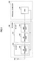
- the wireless LAN apparatus 1000 according to an embodiment of the present invention includes a module group section 1000D having multiple modules of the wireless LAN apparatus 1000 that are subject to a power control operation.
- the modules include, for example, a BB processing part for processing base band signals, a MAC processing part for performing a media access control operation (e.g. CSMA/CA), and an oscillator for transmitting clock signals to each module.
- a BB processing part for processing base band signals
- a MAC processing part for performing a media access control operation (e.g. CSMA/CA)
- an oscillator for transmitting clock signals to each module.
- the wireless LAN apparatus 1000 also includes a power reduction instruction dispatching section 1000A that dispatches instructions (power reduction instructions) instructing to reduce power so as to save on power consumption, a power reduction instruction receiving section 1000B that receives the power reduction instructions from the power reduction instruction dispatching part 1000A, and a power reduction sequence controlling section 1000C that performs power reduction (according to the power reduction signals received in the power reduction receiving section 1000B) and power recovery in a predetermined order.
- a power reduction instruction dispatching section 1000A that dispatches instructions (power reduction instructions) instructing to reduce power so as to save on power consumption
- a power reduction instruction receiving section 1000B that receives the power reduction instructions from the power reduction instruction dispatching part 1000A
- a power reduction sequence controlling section 1000C that performs power reduction (according to the power reduction signals received in the power reduction receiving section 1000B) and power recovery in a predetermined order.
- Fig.3 is a schematic diagram showing an exemplary configuration of a wireless LAN apparatus 500 according to the first embodiment of the present invention.
- the configuration also includes an inside CPU 22 provided inside an IC chip 2 which serves as one of the main parts of the wireless LAN apparatus 500. That is, at least a portion of the workload (operations) of the upper level CPU 1 mounted in an image forming apparatus (upper level apparatus, e.g. printer, copy machine) is allotted to the inside CPU 22 in the IC chip 2, to thereby allow the inside CPU 22 to process the workload of the upper level CPU (outside CPU) 1.
- an image forming apparatus upper level apparatus, e.g. printer, copy machine
- the wireless LAN apparatus 500 includes the IC chip 2 which is connected to the upper level CPU 1 of an image forming apparatus (e.g. printer, copy machine, not shown), an oscillator 3 which transmits clock signals to the IC chip 2, an IC chip 4 which is connected to the IC chip 2, an oscillator 5 which transmits clock signals to the IC chip 4, and an antenna 6. Furthermore, the IC chip 2 includes an outside CPU interface 21 which inputs/outputs signals with respect to the upper level CPU 1, the inside CPU 22 which is provided for reducing the workload of the upper level CPU 1, a MAC processing part 23 which performs media access control (e.g. CSMA/CA), a BB processing part 24 which processes base band signals, and an RF interface 25 which inputs/outputs signals with respect to the IC chip 4.
- the IC chip 4 includes an RF processing part 41 which processes high frequency signals.
- Fig.4 is a schematic diagram showing an exemplary arrangement of functional sections for performing a power control operation with the wireless LAN apparatus 500 according to the first embodiment of the present invention.
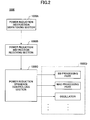
- a power reduction instruction dispatching section 500A is provided for executing a function of the upper level CPU 1.
- a power reduction instruction receiving section 500B and a power reduction sequence controlling section 500C are provided for executing functions of the inside CPU 22.
- a module group section 500D includes the BB processing part 24, the MAC processing part 23, and the oscillators 3, 5.
- Fig.5 is a schematic diagram showing an exemplary configuration of an image forming apparatus 10 (e.g. printer, copy machine) including the wireless LAN apparatus 500 according to the first embodiment of the present invention.
- the image forming apparatus 10 includes a controller board 11 including a function part for performing a controlling operation, an operations panel 16 for receiving input from the user and displaying various operational states, and an engine 17 for performing a printing operation.
- the controller board 11 includes: the upper level CPU 1 for performing the main controlling operations of the image forming apparatus 10; a memory part 13 that includes a ROM (Read Only Memory) for storing fixed data/programs therein, and a RAM (Random Access Memory) serving as a work area; a hard disk part 14 for storing, for example, application programs and printing data; an ASIC (Application Specific Integrated Circuit) 12 for performing an image processing operation; and a wireless LAN interface part 15 including the IC chips 2, 4, and the oscillators 3, 5 and having an antenna 6 connected thereto.
- the upper level CPU 1 for performing the main controlling operations of the image forming apparatus 10
- a memory part 13 that includes a ROM (Read Only Memory) for storing fixed data/programs therein, and a RAM (Random Access Memory) serving as a work area
- a hard disk part 14 for storing, for example, application programs and printing data
- an ASIC (Application Specific Integrated Circuit) 12 for performing an image processing operation
- Fig.6 shows the flow of a power reduction process that is cooperatively performed by the power reduction instruction dispatching section 500A, the power reduction instruction receiving section 500B, and the power reduction sequence controlling section 500C according to the first embodiment of the present invention.
- the upper level CPU 1 dispatches a power reduction instruction to the inside CPU 22 by using the function of the power reduction instruction dispatching section 500A (See Fig.4) when a predetermined power reduction condition is satisfied (e.g. when the wireless LAN is unused for a predetermined period or when reaching a predetermined time) (Step S1).
- the inside CPU 22 When the inside CPU 22 receives the power reduction instruction by using the function of the power instruction receiving section 500B, the inside CPU 22 switches off the power of the MAC processing part 23 and the BB processing part 24 (switched to a "power down state") by using the function of the power reduction sequence controlling section 500C (Steps S2 and S3).
- the inside CPU 22 stops the oscillator 5 by using the function of the power reduction sequence controlling section 500C (Step S4). This prevents clock signals from being transmitted from the RF processing part 41 to the BB processing part 24. However, since the RF processing part 41 is still operable to receive wireless signals, other modules can be restored (activated from the power down state) upon receiving wireless signals.
- the inside CPU 22 stops the oscillator 3 from transmitting clock signals to itself (i.e. stops the transmittal of clock signals from the oscillator 3 to the inside CPU 22) (Step S5) and switches off or reduces its own power (i.e. the power of the inside CPU 22).
- the power of each module can be reduced (turned to the power down state) in a step-by-step manner and the transition to a minimal power state can be achieved while being able to receive wireless signals.
- Fig.7 shows the flow of a process for restoring (reactivating) the power from the power down state according to the first embodiment of the present invention.
- the upper level CPU 1 is in an operational state while the other modules are in an inactive state or at least in a power reduced state.
- the upper level CPU 1 activates the oscillator 3 through the outside CPU interface 21 and the inside CPU 22 (Steps S11 and S12, respectively). Accordingly, the activated oscillator 3 activates the inside CPU 22 by transmitting clock signals to the inside CPU 22.
- the inside CPU 22 activates the oscillator 5 through the RF processing part 41 (Step S13) and also activates the BB processing part 24 and the MAC processing part 23 (Steps S14 and S15, respectively). Accordingly, the activated oscillator 5 transmits clock signals to the RF processing part 41; then the RF processing part 41 transmits clock signals to the BB processing part 24; and then the BB processing part 24 transmits clock signals to the MAC processing part 23. Thereby, the entire system returns to a regular operational state.
- the wireless LAN apparatus 600 according to the second embodiment of the present invention does not include an inside CPU provided in a chip.
- the modules of the wireless LAN apparatus 600 according to the second embodiment of the present invention may be fabricated, for example, as an IC chip or as discrete components (separate components).
- the wireless LAN apparatus 600 includes a CPU 91 included in an upper level apparatus (e.g. printer, copy machine), a MAC processing part 92 that performs a media access control operation (e.g.
- a BB processing part 93 that processes base band signals
- an RF processing part 94 that processes high frequency signals
- an oscillator 95 that transmits clock signals to the RF processing part 94
- an antenna 96 connected to the RF processing part 94.
- Fig.9 is a schematic diagram showing an exemplary arrangement of functional sections for performing a power control operation with the wireless LAN apparatus 600 according to the second embodiment of the present invention.
- a power reduction instruction dispatching section 600A a power reduction instruction receiving section 600B and a power reduction sequence controlling section 600C are provided for executing the functions of the CPU 91.
- a module group section 600D includes the BB processing part 93, the MAC processing part 92, and the oscillator 95.
- Fig.10 shows the flow of a power reduction process that is cooperatively performed by the power reduction instruction dispatching part 600A, the power reduction instruction receiving part 600B, and the power reduction sequence controlling part 600C according to the second embodiment of the present invention.
- the power reduction instruction dispatching section 600A (See Fig.9) in the CPU 91 dispatches a power reduction instruction when a predetermined power reduction condition is satisfied (e.g. when the wireless LAN is unused for a predetermined period or when reaching a predetermined time).
- the power reduction sequence controlling section 600C (See Fig.9) in the CPU 91 switches off or at least reduces the power of the MAC processing part 92 and the BB processing part 93 (switched to a "power down state") (Steps S21 and S22). Then, the power reduction sequence controlling section 600C in the CPU 91 stops the oscillator 95 (Step S23). This prevents clock signals from being transmitted from the RF processing part 94 to the BB processing part 93. However, since the RF processing part 94 is still operable to receive wireless signals, other modules can be restored (activated from the power down state) upon receiving wireless signals.
- Fig.11 shows the flow of a process for restoring (activating) the power from the power down state according to the second embodiment of the present invention.
- the CPU 91 is in an operational state while the other modules are in an inactive state or at least in a power reduced state.
- the CPU 91 activates the oscillator 95 (Step S31) and also activates the BB processing part 93 and the MAC processing part 92 (Steps S32 and S33, respectively).
- the activated oscillator 95 transmits clock signals to the RF processing part 94; then the RF processing part 94 transmits clock signals to the BB processing part 93; and then the BB processing part 93 transmits clock signals to the MAC processing part 92.
- the entire system returns to a regular operational state.
Landscapes
- Engineering & Computer Science (AREA)
- Computer Networks & Wireless Communication (AREA)
- Signal Processing (AREA)
- Power Sources (AREA)
- Small-Scale Networks (AREA)
- Mobile Radio Communication Systems (AREA)
Abstract
Description
- The present invention relates to a wireless LAN apparatus and a semiconductor device for achieving a step-by-step reduction/restoration of power.
- In recent years and continuing, the standardization of wireless LAN (Local Area Network) technology according to IEEE 802.11 (Institute of Electrical and Electronics Engineers 802.11) is growing. Such wireless LAN technology is introduced as an alternative of the conventional wired network technology or as a technology that is to coexist with the wired network technology. The functions of the wireless LAN technology are typically attained by employing a device such as a PC card that follow standards of organizations such as the PCMCIA (Personal Computer Memory Card International Association). The device, such as the PC card, is mainly used by being mounted in a personal computer. For the purpose of saving electrical power, the personal computer includes a function of switching off the power supply to various parts in the personal computer when the personal computer is not used for a predetermined period of time.
- Fig.1 is a schematic view of an exemplary configuration of a related art configuration for controlling the power of a wireless LAN function part. In Fig.1, a
PC card 200, which is mounted in apersonal computer 100, includes integratedIC chips IC chip 201 includes aMAC processing part 202 for performing media access control (e.g. CSMA/CA (Carrier Sense Multiple Access with Collision Avoidance) and a BB (Base Band) processingpart 203 for processing BB (Base Band) signals. TheIC chip 204 includes an RF (Radio Frequency) processing part for processing high frequency (RF: Radio Frequency) signals. In an operation of transmitting wireless signals from anantenna 206 of thePC card 200, transmission signals travel from aCPU 101 of thepersonal computer 100 to theantenna 206 via theMAC processing part 202, theBB processing part 203, and theRF processing part 205. In an operation of receiving wireless signals from theantenna 206, reception signals travel from theantenna 206 to theCPU 101 of thepersonal computer 100 via theRF processing part 205, theBB processing part 203, and theMAC processing part 202. - In an operation for switching off the power of a wireless LAN function part, a signal instructing to switch off the power is transmitted from the
CPU 101 of thepersonal computer 100 to theIC chips PC card 200 at a predetermined timing. In a case of restoring (reactivating) the power, a signal instructing to switch on the power is transmitted from theCPU 101 of thepersonal computer 100 to theIC chips PC card 200 at a predetermined timing. - Owing to growing demands for increasing the functions of office apparatuses, the wireless LAN function is added not only to the personal computer, but also to office apparatuses such as printers and copy machines. The power of printers and copy machines more often tends to be kept in a continuously on-state compared to the power of the personal computer. Accordingly, there is a considerable demand for reducing the power consumption of office apparatuses such as printers and copy machines, and the demand for reducing the power consumption of the wireless LAN function part thereof is no exception. Furthermore, in a case where a personal computer is not being used, shutting down or switching to a sleep mode may not serve as a problem for the user. Meanwhile, it would be inconvenient to completely switch off the functions of printers and copy machines since a printing job, for example, may be ordered at any time via a network connected to the printers and copy machines.
- In controlling the power of the conventional wireless LAN function part of the
personal computer 100 shown in Fig.1, the power of the PC card can only be switched off entirely and switched back on (restored), for example, by having the user perform a prescribed maneuver. Therefore, it is difficult to reduce the consumption of power for the wireless LAN function part. - In order to reduce power as much as possible while maintaining minimal necessary functions, it is possible to control the power for each module included in a wireless LAN apparatus. However, since the wireless LAN function part normally uses multiple clock signals, it is necessary to conceive a control procedure that is able to prevent the multiple clock signals from causing any errors. That is, the wireless LAN apparatus shown in Fig.1 relies on clocks signals for two circuits (systems) in which one of the clock signals is used for the
CPU 101 of thepersonal computer 100 and the other clock signals is used for theRF processing part 205, theBB processing part 203, and theMAC processing part 202. Therefore, it is desired to conceive a control procedure for reducing and restoring the power of each module while taking the multiple clock signals into consideration. - It is a general object of the present invention to provide a wireless LAN apparatus and a semiconductor device that substantially obviates one or more of the problems caused by the limitations and disadvantages of the related art.
- Features and advantages of the present invention will be set forth in the description which follows, and in part will become apparent from the description and the accompanying drawings, or may be learned by practice of the invention according to the teachings provided in the description. Objects as well as other features and advantages of the present invention will be realized and attained by a wireless LAN apparatus and a semiconductor device particularly pointed out in the specification in such full, clear, concise, and exact terms as to enable a person having ordinary skill in the art to practice the invention.
- To achieve these and other advantages and in accordance with the purpose of the invention, as embodied and broadly described herein, the invention provides a wireless LAN apparatus including: a module group section that is connected to an upper level CPU of an upper level apparatus; an RF processing part that is connected to the module group section; a power reduction instruction dispatching section for dispatching a power reduction instruction; a power reduction instruction receiving section for receiving the power reduction instruction dispatched from the power reduction instruction section; and a power reduction sequence controlling section for controlling power of the module group section in a predetermined order in accordance with the power reduction instruction dispatched by the power reduction instruction dispatching section.
- In a wireless LAN apparatus according to an embodiment of the present invention, the module group section may be included in an IC chip having a MAC processing part for conducting media access control, a BB processing part for processing base band signals, and an inside CPU for processing a portion of the workload of the upper level CPU.
- In a wireless LAN apparatus according to an embodiment of the present invention, the upper level CPU may be configured to function as the power reduction instruction dispatching section, wherein the inside CPU may be configured to function as the power reduction instruction receiving section and the power reduction sequence controlling section.
- In a wireless LAN apparatus according to an embodiment of the present invention, the module group section may further include a first oscillator for transmitting a first oscillator clock signal to the inside CPU, and a second oscillator for transmitting a second oscillator clock signal to the RF processing part.
- In a wireless LAN apparatus according to an embodiment of the present invention, the power reduction sequence controlling section may reduce the power of the MAC processing part, the BB processing part, the inside CPU, the first oscillator, and the second oscillator in an order of the MAC processing part, the BB processing part, the second oscillator, the first oscillator, and the inside CPU.
- In a wireless LAN apparatus according to an embodiment of the present invention, the power reduction sequence controlling section may restore the power of the MAC processing part, the BB processing part, the inside CPU, the first oscillator, and the second oscillator in an order of the first oscillator, the inside CPU, the second oscillator, the BB processing part, and the MAC processing part.
- In a wireless LAN apparatus according to an embodiment of the present invention, the module group section may include a MAC processing part for conducting media access control, and a BB processing part for processing base band signals.
- In a wireless LAN apparatus according to an embodiment of the present invention, the upper level CPU may be configured to function as the power reduction instruction dispatching section, the power reduction instruction receiving section and the power reduction sequence controlling section.
- In a wireless LAN apparatus according to an embodiment of the present invention, the module group section may further include an oscillator for transmitting a clock signal to the RF processing part.
- In a wireless LAN apparatus according to an embodiment of the present invention, the power reduction sequence controlling section may reduce the power of the MAC processing part, the BB processing part, and the oscillator in an order of the MAC processing part, the BB processing part, and the oscillator.
- In a wireless LAN apparatus according to an embodiment of the present invention, the power reduction sequence controlling section may restore the power of the MAC processing part, the BB processing part, and the oscillator in an order of the oscillator, the BB processing part, and the MAC processing part.
- Furthermore, the present invention provides a semiconductor device used for a wireless LAN apparatus including a power reduction function, the semiconductor device including: a power reduction instruction receiving section for receiving a power reduction instruction dispatched from the wireless LAN apparatus; and a power reduction sequence controlling section for controlling power of a module group section included in the wireless LAN apparatus in a predetermined order in accordance with the power reduction instruction dispatched by the power reduction instruction dispatching section.
- In a semiconductor apparatus according to an embodiment of the present invention, the semiconductor apparatus may further include a MAC processing part for conducting media access control, a BB processing part for processing base band signals, and an inside CPU for processing a portion of the workload of an upper level CPU of an upper level apparatus connected to the wireless LAN apparatus.
- Other objects and further features of the present invention will be apparent from the following detailed description when read in conjunction with the accompanying drawings.
- Fig.1 is a schematic view showing an exemplary configuration of a related art configuration for controlling the power of a wireless LAN function part;
- Fig.2 is a schematic view showing an exemplary basic configuration of a wireless LAN apparatus according to an embodiment of the present invention;
- Fig.3 is a schematic view showing an exemplary configuration of a wireless LAN apparatus according to the first embodiment of the present invention;
- Fig.4 is a schematic view showing an exemplary arrangement of functional sections for performing a power control operation with a wireless LAN apparatus according to the first embodiment of the present invention;
- Fig.5 is a schematic view showing an exemplary configuration of an image forming apparatus including a wireless LAN according to the first embodiment of the present invention;
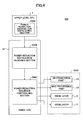
- Fig.6 is a schematic view showing the flow of a power reduction process according to the first embodiment of the present invention;
- Fig.7 is a schematic view showing the flow of a power restoration process according to the first embodiment of the present invention;
- Fig.8 is a schematic view showing an exemplary configuration of a wireless LAN apparatus according to the second embodiment of the present invention;
- Fig.9 is a schematic view showing an exemplary arrangement of functional sections for performing a power control operation with a wireless LAN apparatus according to the second embodiment of the present invention;
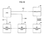
- Fig.10 is a schematic view showing the flow of a power reduction process according to the second embodiment of the present invention; and
- Fig.11 is a schematic view showing the flow of a power restoration process according to the second embodiment of the present invention.
- In the following, embodiments of the present invention will be described with reference to the accompanying drawings.
- Fig.2 shows an exemplary basic configuration of a
wireless LAN apparatus 1000 according to an embodiment of the present invention for controlling electric power thereof. In Fig.2, thewireless LAN apparatus 1000 according to an embodiment of the present invention includes amodule group section 1000D having multiple modules of thewireless LAN apparatus 1000 that are subject to a power control operation. The modules include, for example, a BB processing part for processing base band signals, a MAC processing part for performing a media access control operation (e.g. CSMA/CA), and an oscillator for transmitting clock signals to each module. Thewireless LAN apparatus 1000 also includes a power reductioninstruction dispatching section 1000A that dispatches instructions (power reduction instructions) instructing to reduce power so as to save on power consumption, a power reduction instruction receivingsection 1000B that receives the power reduction instructions from the power reductioninstruction dispatching part 1000A, and a power reductionsequence controlling section 1000C that performs power reduction (according to the power reduction signals received in the powerreduction receiving section 1000B) and power recovery in a predetermined order. The arrangement of the above-described sections is further described below. - Fig.3 is a schematic diagram showing an exemplary configuration of a
wireless LAN apparatus 500 according to the first embodiment of the present invention. In addition to an upper level CPU (outside CPU) 1, the configuration also includes aninside CPU 22 provided inside anIC chip 2 which serves as one of the main parts of thewireless LAN apparatus 500. That is, at least a portion of the workload (operations) of theupper level CPU 1 mounted in an image forming apparatus (upper level apparatus, e.g. printer, copy machine) is allotted to theinside CPU 22 in theIC chip 2, to thereby allow theinside CPU 22 to process the workload of the upper level CPU (outside CPU) 1. This significantly reduces the workload of theupper level CPU 1 and prevents an excess workload from being applied to theupper level CPU 1 of the image forming apparatus (which usually has a lower processing performance than that of a personal computer, for example) in a case where, for example, a wireless LAN function is added. - In Fig.3, the
wireless LAN apparatus 500 includes theIC chip 2 which is connected to theupper level CPU 1 of an image forming apparatus (e.g. printer, copy machine, not shown), anoscillator 3 which transmits clock signals to theIC chip 2, an IC chip 4 which is connected to theIC chip 2, anoscillator 5 which transmits clock signals to the IC chip 4, and anantenna 6. Furthermore, theIC chip 2 includes anoutside CPU interface 21 which inputs/outputs signals with respect to theupper level CPU 1, theinside CPU 22 which is provided for reducing the workload of theupper level CPU 1, aMAC processing part 23 which performs media access control (e.g. CSMA/CA), aBB processing part 24 which processes base band signals, and anRF interface 25 which inputs/outputs signals with respect to the IC chip 4. The IC chip 4 includes anRF processing part 41 which processes high frequency signals. - Fig.4 is a schematic diagram showing an exemplary arrangement of functional sections for performing a power control operation with the
wireless LAN apparatus 500 according to the first embodiment of the present invention. In Fig.4, a power reductioninstruction dispatching section 500A is provided for executing a function of theupper level CPU 1. Furthermore, a power reductioninstruction receiving section 500B and a power reductionsequence controlling section 500C are provided for executing functions of theinside CPU 22. Furthermore, amodule group section 500D includes theBB processing part 24, theMAC processing part 23, and theoscillators - Fig.5 is a schematic diagram showing an exemplary configuration of an image forming apparatus 10 (e.g. printer, copy machine) including the
wireless LAN apparatus 500 according to the first embodiment of the present invention. In Fig.5, theimage forming apparatus 10 includes acontroller board 11 including a function part for performing a controlling operation, anoperations panel 16 for receiving input from the user and displaying various operational states, and an engine 17 for performing a printing operation. Thecontroller board 11 includes: theupper level CPU 1 for performing the main controlling operations of theimage forming apparatus 10; amemory part 13 that includes a ROM (Read Only Memory) for storing fixed data/programs therein, and a RAM (Random Access Memory) serving as a work area; ahard disk part 14 for storing, for example, application programs and printing data; an ASIC (Application Specific Integrated Circuit) 12 for performing an image processing operation; and a wirelessLAN interface part 15 including the IC chips 2, 4, and theoscillators antenna 6 connected thereto. - Fig.6 shows the flow of a power reduction process that is cooperatively performed by the power reduction
instruction dispatching section 500A, the power reductioninstruction receiving section 500B, and the power reductionsequence controlling section 500C according to the first embodiment of the present invention. In Fig.6, theupper level CPU 1 dispatches a power reduction instruction to theinside CPU 22 by using the function of the power reductioninstruction dispatching section 500A (See Fig.4) when a predetermined power reduction condition is satisfied (e.g. when the wireless LAN is unused for a predetermined period or when reaching a predetermined time) (Step S1). When theinside CPU 22 receives the power reduction instruction by using the function of the powerinstruction receiving section 500B, theinside CPU 22 switches off the power of theMAC processing part 23 and the BB processing part 24 (switched to a "power down state") by using the function of the power reductionsequence controlling section 500C (Steps S2 and S3). - Next, the
inside CPU 22 stops theoscillator 5 by using the function of the power reductionsequence controlling section 500C (Step S4). This prevents clock signals from being transmitted from theRF processing part 41 to theBB processing part 24. However, since theRF processing part 41 is still operable to receive wireless signals, other modules can be restored (activated from the power down state) upon receiving wireless signals. Next, theinside CPU 22 stops theoscillator 3 from transmitting clock signals to itself (i.e. stops the transmittal of clock signals from theoscillator 3 to the inside CPU 22) (Step S5) and switches off or reduces its own power (i.e. the power of the inside CPU 22). - Accordingly, the power of each module can be reduced (turned to the power down state) in a step-by-step manner and the transition to a minimal power state can be achieved while being able to receive wireless signals.
- Fig.7 shows the flow of a process for restoring (reactivating) the power from the power down state according to the first embodiment of the present invention. In Fig.7, the
upper level CPU 1 is in an operational state while the other modules are in an inactive state or at least in a power reduced state. First, in the activating process, theupper level CPU 1 activates theoscillator 3 through theoutside CPU interface 21 and the inside CPU 22 (Steps S11 and S12, respectively). Accordingly, the activatedoscillator 3 activates theinside CPU 22 by transmitting clock signals to theinside CPU 22. Then, theinside CPU 22 activates theoscillator 5 through the RF processing part 41 (Step S13) and also activates theBB processing part 24 and the MAC processing part 23 (Steps S14 and S15, respectively). Accordingly, the activatedoscillator 5 transmits clock signals to theRF processing part 41; then theRF processing part 41 transmits clock signals to theBB processing part 24; and then theBB processing part 24 transmits clock signals to theMAC processing part 23. Thereby, the entire system returns to a regular operational state. - Next, a
wireless LAN apparatus 600 according to the second embodiment of the present invention is described with reference to Fig.8. Thewireless LAN apparatus 600 according to the second embodiment of the present invention (unlike thewireless LAN apparatus 500 according to the first embodiment of the present invention) does not include an inside CPU provided in a chip. It is to be noted that the modules of thewireless LAN apparatus 600 according to the second embodiment of the present invention may be fabricated, for example, as an IC chip or as discrete components (separate components). As shown in Fig.8, thewireless LAN apparatus 600 includes aCPU 91 included in an upper level apparatus (e.g. printer, copy machine), aMAC processing part 92 that performs a media access control operation (e.g. CSMA/CA), aBB processing part 93 that processes base band signals, anRF processing part 94 that processes high frequency signals, anoscillator 95 that transmits clock signals to theRF processing part 94, and anantenna 96 connected to theRF processing part 94. - Fig.9 is a schematic diagram showing an exemplary arrangement of functional sections for performing a power control operation with the
wireless LAN apparatus 600 according to the second embodiment of the present invention. In Fig.9, a power reductioninstruction dispatching section 600A, a power reductioninstruction receiving section 600B and a power reductionsequence controlling section 600C are provided for executing the functions of theCPU 91. Furthermore, amodule group section 600D includes theBB processing part 93, theMAC processing part 92, and theoscillator 95. - Fig.10 shows the flow of a power reduction process that is cooperatively performed by the power reduction
instruction dispatching part 600A, the power reductioninstruction receiving part 600B, and the power reductionsequence controlling part 600C according to the second embodiment of the present invention. In Fig.10, the power reductioninstruction dispatching section 600A (See Fig.9) in theCPU 91 dispatches a power reduction instruction when a predetermined power reduction condition is satisfied (e.g. when the wireless LAN is unused for a predetermined period or when reaching a predetermined time). When the power reductioninstruction receiving section 600B (See Fig.9) in theCPU 91 receives the dispatched power reduction instruction, the power reductionsequence controlling section 600C (See Fig.9) in theCPU 91 switches off or at least reduces the power of theMAC processing part 92 and the BB processing part 93 (switched to a "power down state") (Steps S21 and S22). Then, the power reductionsequence controlling section 600C in theCPU 91 stops the oscillator 95 (Step S23). This prevents clock signals from being transmitted from theRF processing part 94 to theBB processing part 93. However, since theRF processing part 94 is still operable to receive wireless signals, other modules can be restored (activated from the power down state) upon receiving wireless signals. - Fig.11 shows the flow of a process for restoring (activating) the power from the power down state according to the second embodiment of the present invention. In Fig.11, the
CPU 91 is in an operational state while the other modules are in an inactive state or at least in a power reduced state. In the activating process, theCPU 91 activates the oscillator 95 (Step S31) and also activates theBB processing part 93 and the MAC processing part 92 (Steps S32 and S33, respectively). Accordingly, the activatedoscillator 95 transmits clock signals to theRF processing part 94; then theRF processing part 94 transmits clock signals to theBB processing part 93; and then theBB processing part 93 transmits clock signals to theMAC processing part 92. Thereby, the entire system returns to a regular operational state. - Further, the present invention is not limited to these embodiments, but various variations and modifications may be made without departing from the scope of the present invention.
Claims (13)
- A wireless LAN apparatus characterized by comprising:a module group section that is connected to an upper level CPU of an upper level apparatus;an RF processing part that is connected to the module group section;a power reduction instruction dispatching section for dispatching a power reduction instruction;a power reduction instruction receiving section for receiving the power reduction instruction dispatched from the power reduction instruction section; anda power reduction sequence controlling section for controlling power of the module group section in a predetermined order in accordance with the power reduction instruction dispatched by the power reduction instruction dispatching section.
- The wireless LAN apparatus as claimed in claim 1, characterized in that the module group section is included in an IC chip having
a MAC processing part for conducting media access control,
a BB processing part for processing base band signals, and
an inside CPU for processing a portion of the workload of the upper level CPU. - The wireless LAN apparatus as claimed in claim 2, characterized in that the upper level CPU is configured to function as the power reduction instruction dispatching section, wherein the inside CPU is configured to function as the power reduction instruction receiving section and the power reduction sequence controlling section.
- The wireless LAN apparatus as claimed in claim 3, characterized in that the module group section further includes
a first oscillator for transmitting a first oscillator clock signal to the inside CPU, and
a second oscillator for transmitting a second oscillator clock signal to the RF processing part. - The wireless LAN apparatus as claimed in claim 4, characterized in that the power reduction sequence controlling section reduces the power of the MAC processing part, the BB processing part, the inside CPU, the first oscillator, and the second oscillator in an order of the MAC processing part, the BB processing part, the second oscillator, the first oscillator, and the inside CPU.
- The wireless LAN apparatus as claimed in claim 5, characterized in that the power reduction sequence controlling section restores the power of the MAC processing part, the BB processing part, the inside CPU, the first oscillator, and the second oscillator in an order of the first oscillator, the inside CPU, the second oscillator, the BB processing part, and the MAC processing part.
- The wireless LAN apparatus according to any one of the preceding claims, characterized in that the module group section includes
a MAC processing part for conducting media access control, and
a BB processing part for processing base band signals. - The wireless LAN apparatus as claimed in claim 7, characterized in that the upper level CPU is configured to function as the power reduction instruction dispatching section, the power reduction instruction receiving section and the power reduction sequence controlling section.
- The wireless LAN apparatus as claimed in claim 8, characterized in that the module group section further includes an oscillator for transmitting a clock signal to the RF processing part.
- The wireless LAN apparatus as claimed in claim 9, characterized in that the power reduction sequence controlling section reduces the power of the MAC processing part, the BB processing part, and the oscillator in an order of the MAC processing part, the BB processing part, and the oscillator.
- The wireless LAN apparatus as claimed in claim 10, characterized in that the power reduction sequence controlling section restores the power of the MAC processing part, the BB processing part, and the oscillator in an order of the oscillator, the BB processing part, and the MAC processing part.
- A semiconductor device used for a wireless LAN apparatus including a power reduction function, the semiconductor device characterized by comprising:a power reduction instruction receiving section for receiving a power reduction instruction dispatched from the wireless LAN apparatus; anda power reduction sequence controlling section for controlling power of a module group section included in the wireless LAN apparatus in a predetermined order in accordance with the power reduction instruction dispatched by the power reduction instruction dispatching section.
- The semiconductor device as claimed in claim 12, further characterized by comprising:a MAC processing part for conducting media access control,a BB processing part for processing base band signals, andan inside CPU for processing a portion of the workload of an upper level CPU of an upper level apparatus connected to the wireless LAN apparatus.
Applications Claiming Priority (1)
| Application Number | Priority Date | Filing Date | Title |
|---|---|---|---|
| JP2004328130A JP2006140738A (en) | 2004-11-11 | 2004-11-11 | Wireless LAN device |
Publications (3)
| Publication Number | Publication Date |
|---|---|
| EP1657825A2 true EP1657825A2 (en) | 2006-05-17 |
| EP1657825A3 EP1657825A3 (en) | 2007-05-02 |
| EP1657825B1 EP1657825B1 (en) | 2016-05-25 |
Family
ID=35519945
Family Applications (1)
| Application Number | Title | Priority Date | Filing Date |
|---|---|---|---|
| EP05256970.4A Expired - Lifetime EP1657825B1 (en) | 2004-11-11 | 2005-11-11 | Wireless lan apparatus and semiconductor device |
Country Status (3)
| Country | Link |
|---|---|
| US (1) | US7539477B2 (en) |
| EP (1) | EP1657825B1 (en) |
| JP (1) | JP2006140738A (en) |
Families Citing this family (2)
| Publication number | Priority date | Publication date | Assignee | Title |
|---|---|---|---|---|
| US8164773B2 (en) | 2006-05-26 | 2012-04-24 | Marvell World Trade Ltd. | Wireless system-in-package and image processing control apparatus |
| KR101602328B1 (en) * | 2014-12-26 | 2016-03-10 | 주식회사 이노와이어리스 | method for controlling electric power of physical layer device for mobile telecommunication system |
Family Cites Families (13)
| Publication number | Priority date | Publication date | Assignee | Title |
|---|---|---|---|---|
| JPH0667766A (en) * | 1992-08-21 | 1994-03-11 | Fujitsu Ltd | Portable terminal equipment |
| JP2000196694A (en) * | 1998-12-25 | 2000-07-14 | Japan Storage Battery Co Ltd | Modem and data communication system |
| JP3455702B2 (en) * | 1999-08-04 | 2003-10-14 | 日本無線株式会社 | Intermittent positioning method and positioning device |
| JP4496817B2 (en) | 2001-02-09 | 2010-07-07 | セイコーエプソン株式会社 | Image processing via network |
| JP3771923B2 (en) | 2001-07-16 | 2006-05-10 | 株式会社リコー | Digital computing device and external device |
| JP2004153359A (en) * | 2002-10-29 | 2004-05-27 | Yokogawa Electric Corp | Radio lan terminal |
| JP2004249687A (en) * | 2003-02-21 | 2004-09-09 | Ricoh Co Ltd | Image forming device |
| US7277417B2 (en) * | 2003-04-29 | 2007-10-02 | Broadcom Corporation | Low power protocol for wireless terminal peer-to-peer communications |
| JP4095501B2 (en) * | 2003-06-25 | 2008-06-04 | インターナショナル・ビジネス・マシーンズ・コーポレーション | Computer apparatus, wireless access point, power-on method via wireless network, frame listening method, frame transmission method, and program |
| KR100771715B1 (en) * | 2003-09-02 | 2007-10-30 | 엘지전자 주식회사 | Wireless communication data communication control device and method |
| KR100542348B1 (en) * | 2003-09-03 | 2006-01-10 | 삼성전자주식회사 | Method and apparatus for reducing power in wireless lan system |
| DE102004009695A1 (en) * | 2004-02-27 | 2005-09-29 | Advanced Micro Devices, Inc., Sunnyvale | Efficient power-saving mode for WLAN communication systems |
| US20070127403A1 (en) * | 2005-12-06 | 2007-06-07 | Mediatek Inc. | Power saving method for WLAN station |
-
2004
- 2004-11-11 JP JP2004328130A patent/JP2006140738A/en active Pending
-
2005
- 2005-11-09 US US11/269,849 patent/US7539477B2/en not_active Expired - Fee Related
- 2005-11-11 EP EP05256970.4A patent/EP1657825B1/en not_active Expired - Lifetime
Non-Patent Citations (1)
| Title |
|---|
| None |
Also Published As
| Publication number | Publication date |
|---|---|
| US7539477B2 (en) | 2009-05-26 |
| JP2006140738A (en) | 2006-06-01 |
| EP1657825B1 (en) | 2016-05-25 |
| US20060121952A1 (en) | 2006-06-08 |
| EP1657825A3 (en) | 2007-05-02 |
Similar Documents
| Publication | Publication Date | Title |
|---|---|---|
| KR100479948B1 (en) | Mobile radio telephone set | |
| CN101626599B (en) | Techiques for management of shared resources in wireless multi-communication devices | |
| EP0887990B1 (en) | Modem unit | |
| US6938108B2 (en) | Micro-controller having USB control unit, MC unit and oscillating circuit commonly used by the USB control unit and the MC unit | |
| US7992019B2 (en) | System device including NIC and power-saving controlling method of the same | |
| EP2544085B1 (en) | Printing apparatus, program, printing system and printing method | |
| GB2332763A (en) | Clock control type information processing apparatus | |
| WO2011048658A1 (en) | Information processing device having a plurality of communication interfaces, and control method of such information processing device | |
| JP2002290340A (en) | Information processing apparatus and clock control method | |
| KR100309941B1 (en) | Wireless handset | |
| US7467307B2 (en) | Electronic circuit and electronic device | |
| EP1657825B1 (en) | Wireless lan apparatus and semiconductor device | |
| JP2009177774A (en) | Signal processing apparatus, portable communication terminal apparatus, and wireless communication system | |
| JP4503512B2 (en) | Radio communication apparatus and power converter operating frequency control method | |
| JP2007047966A (en) | Power saving control system | |
| US20050117550A1 (en) | Information processing device | |
| JP2000112756A (en) | CPU operation control device and method | |
| JP5796374B2 (en) | Image processing apparatus, image processing method, and program | |
| JP4300206B2 (en) | Serial communication control method for mobile communication terminal | |
| JP4413753B2 (en) | Wireless LAN device | |
| US20090083571A1 (en) | System on chip with low power mode and method of driving the same | |
| JP2006236241A (en) | Peripheral device | |
| EP4439292A1 (en) | Method for processing interrupt and interrupt processing device | |
| JP2004282477A (en) | Communication device having asynchronous processor and communication method therefor | |
| US20010016917A1 (en) | Method and configuration for supplying a clock signal to processor-controlled apparatuses |
Legal Events
| Date | Code | Title | Description |
|---|---|---|---|
| PUAI | Public reference made under article 153(3) epc to a published international application that has entered the european phase |
Free format text: ORIGINAL CODE: 0009012 |
|
| 17P | Request for examination filed |
Effective date: 20051121 |
|
| AK | Designated contracting states |
Kind code of ref document: A2 Designated state(s): AT BE BG CH CY CZ DE DK EE ES FI FR GB GR HU IE IS IT LI LT LU LV MC NL PL PT RO SE SI SK TR |
|
| AX | Request for extension of the european patent |
Extension state: AL BA HR MK YU |
|
| PUAL | Search report despatched |
Free format text: ORIGINAL CODE: 0009013 |
|
| AK | Designated contracting states |
Kind code of ref document: A3 Designated state(s): AT BE BG CH CY CZ DE DK EE ES FI FR GB GR HU IE IS IT LI LT LU LV MC NL PL PT RO SE SI SK TR |
|
| AX | Request for extension of the european patent |
Extension state: AL BA HR MK YU |
|
| RIC1 | Information provided on ipc code assigned before grant |
Ipc: H04B 1/16 20060101ALI20070323BHEP Ipc: H04L 12/28 20060101AFI20070323BHEP |
|
| 17Q | First examination report despatched |
Effective date: 20070802 |
|
| AKX | Designation fees paid |
Designated state(s): DE FR GB IT |
|
| REG | Reference to a national code |
Ref country code: DE Ref legal event code: R079 Ref document number: 602005049411 Country of ref document: DE Free format text: PREVIOUS MAIN CLASS: H04B0001160000 Ipc: H04W0052020000 |
|
| GRAP | Despatch of communication of intention to grant a patent |
Free format text: ORIGINAL CODE: EPIDOSNIGR1 |
|
| RIC1 | Information provided on ipc code assigned before grant |
Ipc: H04W 52/02 20090101AFI20160114BHEP |
|
| INTG | Intention to grant announced |
Effective date: 20160203 |
|
| GRAS | Grant fee paid |
Free format text: ORIGINAL CODE: EPIDOSNIGR3 |
|
| GRAA | (expected) grant |
Free format text: ORIGINAL CODE: 0009210 |
|
| AK | Designated contracting states |
Kind code of ref document: B1 Designated state(s): DE FR GB IT |
|
| REG | Reference to a national code |
Ref country code: GB Ref legal event code: FG4D |
|
| REG | Reference to a national code |
Ref country code: DE Ref legal event code: R096 Ref document number: 602005049411 Country of ref document: DE |
|
| REG | Reference to a national code |
Ref country code: FR Ref legal event code: PLFP Year of fee payment: 12 |
|
| PG25 | Lapsed in a contracting state [announced via postgrant information from national office to epo] |
Ref country code: IT Free format text: LAPSE BECAUSE OF FAILURE TO SUBMIT A TRANSLATION OF THE DESCRIPTION OR TO PAY THE FEE WITHIN THE PRESCRIBED TIME-LIMIT Effective date: 20160525 |
|
| REG | Reference to a national code |
Ref country code: DE Ref legal event code: R097 Ref document number: 602005049411 Country of ref document: DE |
|
| PLBE | No opposition filed within time limit |
Free format text: ORIGINAL CODE: 0009261 |
|
| STAA | Information on the status of an ep patent application or granted ep patent |
Free format text: STATUS: NO OPPOSITION FILED WITHIN TIME LIMIT |
|
| 26N | No opposition filed |
Effective date: 20170228 |
|
| REG | Reference to a national code |
Ref country code: FR Ref legal event code: PLFP Year of fee payment: 13 |
|
| PGFP | Annual fee paid to national office [announced via postgrant information from national office to epo] |
Ref country code: DE Payment date: 20191121 Year of fee payment: 15 |
|
| PGFP | Annual fee paid to national office [announced via postgrant information from national office to epo] |
Ref country code: FR Payment date: 20191120 Year of fee payment: 15 |
|
| PGFP | Annual fee paid to national office [announced via postgrant information from national office to epo] |
Ref country code: GB Payment date: 20191120 Year of fee payment: 15 |
|
| REG | Reference to a national code |
Ref country code: DE Ref legal event code: R119 Ref document number: 602005049411 Country of ref document: DE |
|
| GBPC | Gb: european patent ceased through non-payment of renewal fee |
Effective date: 20201111 |
|
| PG25 | Lapsed in a contracting state [announced via postgrant information from national office to epo] |
Ref country code: FR Free format text: LAPSE BECAUSE OF NON-PAYMENT OF DUE FEES Effective date: 20201130 |
|
| PG25 | Lapsed in a contracting state [announced via postgrant information from national office to epo] |
Ref country code: GB Free format text: LAPSE BECAUSE OF NON-PAYMENT OF DUE FEES Effective date: 20201111 Ref country code: DE Free format text: LAPSE BECAUSE OF NON-PAYMENT OF DUE FEES Effective date: 20210601 |