EP1657823A1 - Floating point IDAC - Google Patents
Floating point IDAC Download PDFInfo
- Publication number
- EP1657823A1 EP1657823A1 EP04392040A EP04392040A EP1657823A1 EP 1657823 A1 EP1657823 A1 EP 1657823A1 EP 04392040 A EP04392040 A EP 04392040A EP 04392040 A EP04392040 A EP 04392040A EP 1657823 A1 EP1657823 A1 EP 1657823A1
- Authority
- EP
- European Patent Office
- Prior art keywords
- current
- digital
- output
- exponent
- analog
- Prior art date
- Legal status (The legal status is an assumption and is not a legal conclusion. Google has not performed a legal analysis and makes no representation as to the accuracy of the status listed.)
- Granted
Links
- 238000000034 method Methods 0.000 claims abstract description 33
- 101100129500 Caenorhabditis elegans max-2 gene Proteins 0.000 claims description 12
- 230000002596 correlated effect Effects 0.000 claims description 10
- 230000001419 dependent effect Effects 0.000 claims description 10
- 230000000875 corresponding effect Effects 0.000 claims description 2
- 238000005516 engineering process Methods 0.000 claims description 2
- 230000003213 activating effect Effects 0.000 claims 2
- 230000003247 decreasing effect Effects 0.000 claims 1
- 230000004048 modification Effects 0.000 claims 1
- 238000012986 modification Methods 0.000 claims 1
- 238000006243 chemical reaction Methods 0.000 abstract description 14
- 238000010586 diagram Methods 0.000 description 6
- 230000007423 decrease Effects 0.000 description 3
- 239000003795 chemical substances by application Substances 0.000 description 1
- 239000000463 material Substances 0.000 description 1
- 238000010606 normalization Methods 0.000 description 1
- 230000008520 organization Effects 0.000 description 1
- 230000000007 visual effect Effects 0.000 description 1
Images



Classifications
-
- H—ELECTRICITY
- H03—ELECTRONIC CIRCUITRY
- H03M—CODING; DECODING; CODE CONVERSION IN GENERAL
- H03M1/00—Analogue/digital conversion; Digital/analogue conversion
- H03M1/66—Digital/analogue converters
- H03M1/664—Non-linear conversion not otherwise provided for in subgroups of H03M1/66
Definitions
- the sign of a binary floating-point number is represented by a single bit. A "1" indicates a negative number, and a “0" indicates a positive number.
- the exponents are stored as 8-bit unsigned integers with a bias of 127.
- the exponent is added to 127 and the sum is represented binary.
- the exponent is 4.
- Added to 127 results in 131 and is represented by the string of 10000011.
- Fig. 2 prior art shows a converter 20 converting a digital floating-point number 21 into an analog signal 25.
- a digital floating point to integer converter 22 and additionally a high resolution digital-to-analog converter 24 were required to convert a digital floating point number into an analog signal.
- the digital floating point to integer converter 22 converts the digital floating-point number 21 into a correspondent integer number 23.
- the high-resolution digital-to-analog converter 24 converts then in a second step this integer number 23 into an analog output signal 25.
- U. S. Patent (4,393,369 to Davies) describes the digitizing of analog signals over a wide dynamic range for a floating-point decimal conversion.
- the widely fluctuating input analog voltages are converted to currents to prevent saturation of circuit elements and are, first, compared with a derived reference signal to produce positive voltages or negative voltages if the input signal exceeds or is less than the derived reference current.
- the positive and negative voltages are fed to a combined floating point processing unit and microprocessor, which generates two groups of digital signals.
- the first group is representative of m mantissa increments and the second group of n signals is indicative of the order of magnitude of the mantissa components.
- a mantissa digital-to-analog current generator and an order of magnitude digital-to-analog current generator are coupled in series with respect to each other to provide the derived reference current, which is to be compared with the next sample of the input analog signal. Since the derived reference current is derived in the immediately preceding sample period, the newly sampled analog signal is compared as being greater or lesser with a still newer input sample.
- the first group of digital signals indicative of the mantissa increments and the second group of digital signals indicative of the order of magnitude are fed onto following circuitry to allow for example, a visual readout or further processing.
- the floating-point analog-to-digital conversion has the great advantage over linear, analog arithmetic conversion by being able to handle large dynamic ranges of analog input signals.
- U. S. Patent (4,278,964 to Vanderford) discloses a methodology and apparatus for converting wide dynamic amplitude range digital data recorded in floating point digital word form, comprising a binary coded mantissa and a binary coded exponent, to an analog signal, or oscillogram, of selectively compressed and/or amplified dynamic amplitude range.
- the digital word occupying a number of binary bit positions, is, in algebraic form, .+-.AG.sup.E ; where A represents the mantissa, or argument, G represents the base, or radix, of the number system used and E represents the exponent.
- the base G is constant, for example at 8, the only binary bits that need to be recorded are those representing the mantissa A and the exponent E.
- the methodology employed to accomplish such reconversion is to change either, or both, the mantissa A and base, or radix, G in such a way that the dynamic range is compressed and, yet, any distortion thereby introduced is minimal. Apparatus for performing the aforesaid changes, among other things, is disclosed.
- U. S. Patent (4,240,070 to Helbig et al.) teaches an apparatus and method providing for an improvement to a system which converts wide amplitude range digital data recorded in floating point digital word form to analog signals within a limited amplitude range.
- the apparatus and method provides for the situation wherein the digital data can represent an analog signal for which on a general decrease in amplitude increases may be superimposed.
- the apparatus includes a digital/analog converter whose reference voltage is individually determined for each sample. This reference voltage is taken from a saw tooth oscillator at an instant of time determined by a delay timer, which responds to changes, with respect to a desired average amplitude, of the actual amplitude of the converted data.
- a principal object of the present invention is to achieve a method to convert directly a digital floating-point number to an analog current.
- Another principal object of the present invention is to achieve a circuit to convert a digital floating-point number directly to an analog current having a high dynamic range and requiring a minimum of chip space.
- a method to convert a digital floating-point number directly into an analog signal comprises, first, to provide a linear current digital-to-analog converter cascaded with an exponential current digital-to-analog converter.
- the next steps of the method invented are to split a floating-point number into its mantissa and exponent, to convert said exponent to a current representing an analog signal of the exponent using said exponential current digital-to-analog converter, and to convert said digital floating point number into an analog current by converting said mantissa by said linear current digital-to-analog converter using the output current of the previous step as biasing reference current.
- the sign bit of the floating-point number can define the direction of the output current via a current direction switch block.
- an alternative method to convert a digital floating point number directly into an analog signal comprises, first, to provide an exponential current digital-to-analog converter cascaded with a linear current digital-to-analog converter.
- the following steps of this method are to split a floating-point number into its mantissa and exponent, to convert said mantissa to a current representing an analog signal of the mantissa using said linear current digital-to-analog converter, and convert said digital floating point number into an analog current by converting said exponent by said exponential current digital-to-analog converter using the output current of the previous step as biasing reference current.
- a circuit to convert digital floating-point numbers into an analog current signal comprises, first, an exponential current digital-to-analog converter, having an input and an output, wherein the input is a vector comprising the bits of the exponent of said floating-point number and the output is an analog current being correlated to the exponential value of said exponent.
- the converter comprises a linear current digital-to-analog converter having inputs and an output, wherein the inputs comprise a vector comprising the mantissa of said floating point number and said analog output current of said exponential current digital-to-analog converter and the output comprises an analog current being linearly correlated to the value of said digital floating point number.
- This alternative circuit comprises, first, a linear current digital-to-analog converter, having an input and an output, wherein the input is a vector comprising the bits of the mantissa of said floating point number and the output is an analog current being correlated to the linear value of said mantissa.
- this alternative circuit comprises an exponential current digital-to analog converter having inputs and an output, wherein the inputs comprise a vector describing the exponent of said floating-point number and said analog output current of said linear current digital-to-analog converter and the output comprises an analog current being linearly correlated to the value of said digital floating point number, and, finally, a means to convert the direction of the output current dependent upon the sign of said floating-point number.
- the preferred embodiments of the present invention disclose novel methods and circuits for conversion of a floating-point number into a corresponding analog current.
- Fig. 3 shows a principal block diagram of the converter 30 of the present invention.
- the conversion of the present invention is performed directly using two cascaded current digital-to-analog converters (IDACs).
- IDACs current digital-to-analog converters
- a first IDAC 31 is converting the exponent of the incoming binary floating-point number 21 and a second low resolution linear IDAC 32 converts the mantissa of the incoming binary floating-point number 21.
- a biasing current I 0 is flowing into the exponential IDAC 31.
- the input signals of this exponential IDAC 31 are (max-min+1) bits from the exponent e i [max...min] of the incoming binary floating-point number 21 wherein i signifies the significant bits of the exponent ranging from the maximal (max) or most significant bit (MSB) at the left of the bit-string of the exponent to the minimum (min) or least significant bit (LSB) to the right of the exponent. Additionally, if required, the sign bit of the floating-point number 21 can define the direction of the output current via a current direction switch block 33.
- the output current of the exponential IDAC 31 is the biasing reference current of the low resolution linear IDAC 32.
- the low resolution linear IDAC 32 provides the mantissa values to the current I 1 and generates a current I representing an analog signal converted from the incoming binary floating-point number 21:
- m represents the mantissa of the incoming digital floating point number 21, and m i ⁇ ⁇ 0, 1 ⁇ represent the bit positions of the mantissa wherein i is ranging from zero position to the maximum n m position of the mantissa.
- This means m i are components of a vector of n m +1 bits.
- the output current I of the converter 30 of the present invention represents an analog output signal converted from an incoming digital floating-point number 21 .
- the current direction switch block 33 controls the direction of the output current I dependent upon the sign bit of the incoming floating point number; the output current is either sunk or sourced.
- sequence of blocks 31 and 32 is commutative. This means that the sequence of blocks 31 and 32 can be interchanged in an alternative embodiment of the invention.
- the conversion of the mantissa, performed by the linear IDAC of block 32 provides the biasing current for the exponential IDAC of block 31, performing the conversion of the exponent.
- the output of the exponential IDAC 31 can then be used for the current direction switch of block 33 according to the sign bit of the incoming floating point number.
- One key advantage of the present invention is that a conversion from a floating-point number to an integer number prior to digital-to analog conversion is no more required.
- the cascaded digital-to-analog converter of the present invention has a high dynamic range and requires less chip area than prior art solutions.
- Fig. 4a illustrates the method steps of a preferred embodiment of the present invention.
- Step 40 describes the provision of a linear current digital-to-analog converter cascaded with an exponential current digital-to-analog converter.
- an incoming floating-point number is split into its mantissa and exponent.
- said exponent of the incoming floating point number is converted to a current representing an analog signal of the exponent using said exponential current digital-to-analog converter and in step 43 said digital floating point number is converted into an analog current by converting said mantissa by said linear current digital-to-analog converter using the output current of the previous step as biasing reference current.
- the direction of the output current can be set in step 44 dependent upon the sign bit as described above. This can be advantageous for some applications.
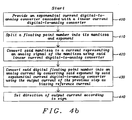
- Fig. 4b illustrates the method steps of an alternative embodiment of the present invention.
- the sequence of the linear and exponential conversion can be interchanged.
- the output current of a linear IDAC is used as a biasing current of an exponential IDAC.
- Step 400 of Fig. 4b describes the provision of an exponential current digital-to-analog converter cascaded with a linear current digital-to-analog converter.
- step 410 an incoming floating-point number is split into its mantissa and exponent.
- step 420 said mantissa of the incoming floating point number is converted to a current representing an analog signal of the mantissa using said linear current digital-to-analog converter and in step 430 said digital floating point number is converted into an analog current by converting said exponent by said exponential current digital-to-analog converter using the output current of the previous step as biasing reference current. If required the direction of the output current can be set in step 440 dependent upon the sign bit as described above. This can be advantageous for some applications.
- Fig. 5 shows a schematic of the circuit of a preferred embodiment of a 4-bit exponential current digital-to analog converter 50.
- the converter 50 shown in Fig. 5 corresponds to the converter 30 as shown in Fig. 3 and is an important part of the present invention. It has to be understood that by cascading the circuit of Fig. 5 more bits could be exponentially converted to an analog current and vice versa less bits can be converted by omitting some stages.
- the current source 51 provides the biasing current 10 for the converter 50 according to 10 of equation (1)
- the transistors N10 and N20 form a current mirror wherein N10 is the input transistor and N20 is the output transistor.
- Transistor N11 can be switched in parallel to transistor N10 by switching N12 ON by the LSB bit e -2 of the exponent to be converted.
- Transistor N21 can be switched in parallel to transistor N20 by switching transistor N22 ON by the e -1 bit of the exponent.
- Dependent upon the status of the bits e -2 and e -1 the transistors of the current mirror N10/N20 can be made wider and thus the related current mirror ratio can be changed.
- Other relationships of the width of transistors N10, and N20 are possible as well to provide a scaling of the output current. But the relationships of the pairs (N10, N11) and (N20, N21) have to accord to the formulas above.
- N12 and/or N22 ON and OFF the width of N10 and N20 will be changed and accordingly the ratio of the current mirror N10/N20 will be changed.
- transistor N12 is switched on by the LSB bit e -2 and transistor N21 is still switched off, the width of the input transistor N10 of the current mirror N10/N20 will be increased and the output current will be reduced by the factor 2-0.25
- transistor N22 is switched on by the LSB bit e -1 the width of the output transistor N20 of the current mirror N10/N20 will be increased and the output current will be increased by the factor 2 0.5
- the current mirror P10/P20 operates principally the same way as the current mirror N10/N20 described above.
- the bit e 0 can switch OFF transistor P12 and thus decreases the width of the input transistor P10 of the current mirror P10/P20.
- the inverted bit e 1 can switch OFF transistor P22 and thus decreases the width of the output transistor P20 of the current mirror P10/P20. As shown in Fig. 5 the signal of bit e 1 is inverted.
- NMOS transistors N10 to N12 and N20 to N22 could be replaced by PMOS transistors while concurrently replacing accordingly the PMOS transistors P10 to P12 and P20 to P22 by NMOS transistors. All inputs e i would have to be inverted.
- the 4-bit exponential digital-to-analog converter is an example of the present invention. More or less bits are feasible by cascading more stages (or current mirrors) or omitting some stages.
- the ratios of the current mirrors must be of the form 2 2 i , wherein i is an integer number.
- the width of the switchable transistors (like N11, N21, P11, and P21 ) of the current mirrors to increase the width of the correspondent transistor of the current mirror has to be 22 2 i -1 related to the width of the correspondent transistor of a current mirror, wherein i is the index of the according bit of the input exponent vector.
- NST int ( n + 1 2 ) .
- a transistor switch and a transistor, which is in parallel to an input or output transistor of a current mirror is required.
- Said transistor switch can switch ON the transistor being parallel to a current mirror transistor to increase the width of said current mirror transistor and thus to modify the ratio of this current mirror.
- the current mirrors are deployed using by turns NMOS and PMOS technology for each stage.
- Another alternative is to omit the current switch N22 and the correspondent current extension transistor N21.
- the output current I 1 of the exponential digital-to-analog converter 50 is fed into a standard linear current digital-to-analog converter 32 which is converting the mantissa of the incoming digital floating point number.
- This linear current digital-to-analog converter 32 can be a low resolution DAC.
- the output current I 1 is biasing the linear current digital-to-analog converter 32. Therefore the output current I of the linear current digital-to-analog converter 32 is an analog signal directly correlated to the incoming digital floating-point number.
- the sequence of the linear digital-to-analog converter and of the exponential digital-to-analog converter can be interchanged.
- the output current of said standard linear digital-to-analog converter which is converting the mantissa of the floating point number
- the exponential current digital-to-analog converter which is converting the exponent of the floating point number using the output current of the linear converter as biasing current.
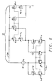
- Fig. 6 illustrates how to consider the sign bit of an incoming floating-point number.
- the output current I SIGN is either sunk or sourced.
- Current I is the output current of the linear IDAC as shown in Fig. 3.
- Both switches S SI are controlled in parallel by the sign bit of the incoming floating point number.
- Dependent upon the position of the switches S SI the direction of the output current I SIGN remains unchanged compared to current I or the current I is directed through current mirror M and the output current I SIGN has a opposite direction compared to current I .
- One key advantage of the present invention is that the floating point number is directly converted into an analog current and no digital floating-point to integer conversion is necessary.
- the solution invented requires less chip area than a high resolution DAC, required in prior art.
Landscapes
- Physics & Mathematics (AREA)
- Nonlinear Science (AREA)
- Engineering & Computer Science (AREA)
- Theoretical Computer Science (AREA)
- Analogue/Digital Conversion (AREA)
Abstract
Description
- This invention relates generally to digital-to-analog converters, and more particularly to a current digital-to-analog converter converting digital floating-point numbers directly into an analog signal.
- In conventional algebraic form a floating-point number is represented by: F = ± M x BE, wherein F represents the absolute magnitude of the floating point number, M represents the mantissa portion of the number, B represents the base of the number system (B=10 in the decimal system), and E represents the exponent.
- There are different floating-point storage formats known. One of the most common formats is the INTEL Short Real format, also called single precision format, which has being standardized by the IEEE organization. As example, the short real format, having 32 bits, is shown in Fig. 1. It has 1 bit for the sign, 8 bits for the exponent and 23 bits for the mantissa.
- The sign of a binary floating-point number is represented by a single bit. A "1" indicates a negative number, and a "0" indicates a positive number.
- An example is used to describe the representation of a mantissa. Using -3.75x10⁴ as an example, the sign is negative therefore the sign bit is ON. The mantissa in this example is 3.75 and the exponent is 4. The fractional portion of the mantissa is the sum of each digit multiplied with the power of 10:

- In regard to a binary floating-point representation of the example of the mantissa 3.75, the fractional portion of the mantissa is the sum of successive powers of 2.

- Combined with the left-hand side of the mantissa the binary floating number looks now 11.11, which is in decimal terms 3.75.
- In IEEE Short Real format the exponents are stored as 8-bit unsigned integers with a bias of 127. The exponent is added to 127 and the sum is represented binary. Using the example shown above the exponent is 4. Added to 127 results in 131 and is represented by the string of 10000011.
- Another common format for digital floating point numbers is the IEEE Long Real format, also called double precision, having 64 bits: 1 bit for the sign, 11 bits for the exponent and 52 bits for the mantissa.
- Before storing a binary floating-point number its mantissa has to be normalized. The normalization is performed in a way that only one digit appears before the decimal. The exponent expresses the number of positions the decimal point was moved left.
- Fig. 2 prior art shows a converter 20 converting a digital floating-
point number 21 into ananalog signal 25. In prior art a digital floating point to integerconverter 22 and additionally a high resolution digital-to-analog converter 24 were required to convert a digital floating point number into an analog signal. The digital floating point to integerconverter 22 converts the digital floating-point number 21 into acorrespondent integer number 23. The high-resolution digital-to-analog converter 24 converts then in a second step thisinteger number 23 into ananalog output signal 25. - It is a challenge for the designers of such solution to find less expensive converters to convert digital floating-point numbers into analog signals.
- There are patents known describing the conversion of floating point numbers it analog signals.
- U. S. Patent (4,393,369 to Davies) describes the digitizing of analog signals over a wide dynamic range for a floating-point decimal conversion. The widely fluctuating input analog voltages are converted to currents to prevent saturation of circuit elements and are, first, compared with a derived reference signal to produce positive voltages or negative voltages if the input signal exceeds or is less than the derived reference current. The positive and negative voltages are fed to a combined floating point processing unit and microprocessor, which generates two groups of digital signals. The first group is representative of m mantissa increments and the second group of n signals is indicative of the order of magnitude of the mantissa components. A mantissa digital-to-analog current generator and an order of magnitude digital-to-analog current generator are coupled in series with respect to each other to provide the derived reference current, which is to be compared with the next sample of the input analog signal. Since the derived reference current is derived in the immediately preceding sample period, the newly sampled analog signal is compared as being greater or lesser with a still newer input sample. The first group of digital signals indicative of the mantissa increments and the second group of digital signals indicative of the order of magnitude are fed onto following circuitry to allow for example, a visual readout or further processing. The floating-point analog-to-digital conversion has the great advantage over linear, analog arithmetic conversion by being able to handle large dynamic ranges of analog input signals.
- U. S. Patent (4,278,964 to Vanderford) discloses a methodology and apparatus for converting wide dynamic amplitude range digital data recorded in floating point digital word form, comprising a binary coded mantissa and a binary coded exponent, to an analog signal, or oscillogram, of selectively compressed and/or amplified dynamic amplitude range. The digital word, occupying a number of binary bit positions, is, in algebraic form, .+-.AG.sup.E ; where A represents the mantissa, or argument, G represents the base, or radix, of the number system used and E represents the exponent. Since the base G is constant, for example at 8, the only binary bits that need to be recorded are those representing the mantissa A and the exponent E. In reconverting the digital data to analog form for making an oscillogram, or wiggle trace, it is desired to selectively amplify and/or compress the dynamic range and, yet, at the same time avoid introducing serious distortion. The methodology employed to accomplish such reconversion is to change either, or both, the mantissa A and base, or radix, G in such a way that the dynamic range is compressed and, yet, any distortion thereby introduced is minimal. Apparatus for performing the aforesaid changes, among other things, is disclosed.
- U. S. Patent (4,240,070 to Helbig et al.) teaches an apparatus and method providing for an improvement to a system which converts wide amplitude range digital data recorded in floating point digital word form to analog signals within a limited amplitude range. The apparatus and method provides for the situation wherein the digital data can represent an analog signal for which on a general decrease in amplitude increases may be superimposed. The apparatus includes a digital/analog converter whose reference voltage is individually determined for each sample. This reference voltage is taken from a saw tooth oscillator at an instant of time determined by a delay timer, which responds to changes, with respect to a desired average amplitude, of the actual amplitude of the converted data.
- A principal object of the present invention is to achieve a method to convert directly a digital floating-point number to an analog current.
- Another principal object of the present invention is to achieve a circuit to convert a digital floating-point number directly to an analog current having a high dynamic range and requiring a minimum of chip space.
- In accordance with the objects of this invention a method to convert a digital floating-point number directly into an analog signal has been achieved. The method invented comprises, first, to provide a linear current digital-to-analog converter cascaded with an exponential current digital-to-analog converter. The next steps of the method invented are to split a floating-point number into its mantissa and exponent, to convert said exponent to a current representing an analog signal of the exponent using said exponential current digital-to-analog converter, and to convert said digital floating point number into an analog current by converting said mantissa by said linear current digital-to-analog converter using the output current of the previous step as biasing reference current. Additionally, if required, the sign bit of the floating-point number can define the direction of the output current via a current direction switch block.
- In accordance with the objects of the invention an alternative method to convert a digital floating point number directly into an analog signal has been achieved. This method invented comprises, first, to provide an exponential current digital-to-analog converter cascaded with a linear current digital-to-analog converter. The following steps of this method are to split a floating-point number into its mantissa and exponent, to convert said mantissa to a current representing an analog signal of the mantissa using said linear current digital-to-analog converter, and convert said digital floating point number into an analog current by converting said exponent by said exponential current digital-to-analog converter using the output current of the previous step as biasing reference current.
- In accordance with the objects of this invention a circuit to convert digital floating-point numbers into an analog current signal has been achieved. This circuit invented comprises, first, an exponential current digital-to-analog converter, having an input and an output, wherein the input is a vector comprising the bits of the exponent of said floating-point number and the output is an analog current being correlated to the exponential value of said exponent. Secondly the converter comprises a linear current digital-to-analog converter having inputs and an output, wherein the inputs comprise a vector comprising the mantissa of said floating point number and said analog output current of said exponential current digital-to-analog converter and the output comprises an analog current being linearly correlated to the value of said digital floating point number.
- In accordance with the objects of this invention an alternative circuit to convert digital floating point numbers into an analog current signal has been achieved. This alternative circuit comprises, first, a linear current digital-to-analog converter, having an input and an output, wherein the input is a vector comprising the bits of the mantissa of said floating point number and the output is an analog current being correlated to the linear value of said mantissa. Furthermore this alternative circuit comprises an exponential current digital-to analog converter having inputs and an output, wherein the inputs comprise a vector describing the exponent of said floating-point number and said analog output current of said linear current digital-to-analog converter and the output comprises an analog current being linearly correlated to the value of said digital floating point number, and, finally, a means to convert the direction of the output current dependent upon the sign of said floating-point number.
- In the accompanying drawings forming a material part of this description, there is shown:
- Fig. 1 shows the structure of a floating-point number.
- Fig. 2 prior art illustrates a block diagram of a prior art digital-to-analog converter of a floating-point number.
- Fig. 3 illustrates a block diagram of the present invention of a digital-to-analog converter of floating-point numbers.
- Fig. 4a shows a flowchart of the method invented to convert a digital floating-point number to an analog current.
- Fig. 4b shows a flowchart of an alternative method invented to convert a digital floating-point number to an analog current.
- Fig. 5 illustrates a circuit diagram of a preferred embodiment of an exponential current digital-to-analog converter of the present invention.
- Fig. 6 illustrates a circuit diagram of a of a current direction switch block being able to convert the direction of the output current dependent on the sign of a floating point number to be converted.
- The preferred embodiments of the present invention disclose novel methods and circuits for conversion of a floating-point number into a corresponding analog current.
- Fig. 3 shows a principal block diagram of the
converter 30 of the present invention. Instead of using a digital floating-point-to-integer converter and additionally a high resolution digital-to-analog converter as showed in Fig. 2 prior art the conversion of the present invention is performed directly using two cascaded current digital-to-analog converters (IDACs). Afirst IDAC 31 is converting the exponent of the incoming binary floating-point number 21 and a second low resolutionlinear IDAC 32 converts the mantissa of the incoming binary floating-point number 21. A biasing current I0 is flowing into theexponential IDAC 31. The input signals of thisexponential IDAC 31 are (max-min+1) bits from the exponent ei [max...min] of the incoming binary floating-point number 21 wherein i signifies the significant bits of the exponent ranging from the maximal (max) or most significant bit (MSB) at the left of the bit-string of the exponent to the minimum (min) or least significant bit (LSB) to the right of the exponent. Additionally, if required, the sign bit of the floating-point number 21 can define the direction of the output current via a currentdirection switch block 33. - The exponential IDAC converts the incoming exponent ei [max...min] into an output current I 1 :

wherein I 1 is the output current of theexponential IDAC 31, I0 is the biasing current of the exponential converter, e j ∈ {0, 1} represent the significant bit positions of the exponent wherein i is ranging from the MSB bit, signified by "max" to the LSB bit, signified by "min". This means e j are components of a vector of (max - min + 1) bits. The output current of theexponential IDAC 31 is the biasing reference current of the low resolutionlinear IDAC 32. - The low resolution
linear IDAC 32 converts the mantissa of the incoming digital floating-point number 21 into binary values. Using the reference current I 1 from the exponential IDAC 31
wherein I1 represents the exponent of the incoming binary floating-point number 21. The low resolutionlinear IDAC 32 provides the mantissa values to the current I 1 and generates a current I representing an analog signal converted from the incoming binary floating-point number 21:
wherein
exponential IDAC 31, m represents the mantissa of the incoming digital floatingpoint number 21, and m i ∈ {0, 1} represent the bit positions of the mantissa wherein i is ranging from zero position to the maximum nm position of the mantissa. This means m i are components of a vector of nm+1 bits. - The output current I of the
converter 30 of the present invention represents an analog output signal converted from an incoming digital floating-point number 21. According to the sign bit the currentdirection switch block 33 controls the direction of the output current I dependent upon the sign bit of the incoming floating point number; the output current is either sunk or sourced. - It has to be understood that the sequence of
blocks blocks block 32 provides the biasing current for the exponential IDAC ofblock 31, performing the conversion of the exponent. The output of theexponential IDAC 31 can then be used for the current direction switch ofblock 33 according to the sign bit of the incoming floating point number. - One key advantage of the present invention is that a conversion from a floating-point number to an integer number prior to digital-to analog conversion is no more required. The cascaded digital-to-analog converter of the present invention has a high dynamic range and requires less chip area than prior art solutions.
- Fig. 4a illustrates the method steps of a preferred embodiment of the present invention.
Step 40 describes the provision of a linear current digital-to-analog converter cascaded with an exponential current digital-to-analog converter. Instep 41 an incoming floating-point number is split into its mantissa and exponent. Instep 42 said exponent of the incoming floating point number is converted to a current representing an analog signal of the exponent using said exponential current digital-to-analog converter and instep 43 said digital floating point number is converted into an analog current by converting said mantissa by said linear current digital-to-analog converter using the output current of the previous step as biasing reference current. If required the direction of the output current can be set in step 44 dependent upon the sign bit as described above. This can be advantageous for some applications. - Fig. 4b illustrates the method steps of an alternative embodiment of the present invention. As described above, according to the commutative property of the present invention, the sequence of the linear and exponential conversion can be interchanged. In this alternative embodiment the output current of a linear IDAC is used as a biasing current of an exponential IDAC. Step 400 of Fig. 4b describes the provision of an exponential current digital-to-analog converter cascaded with a linear current digital-to-analog converter. In
step 410 an incoming floating-point number is split into its mantissa and exponent. Instep 420 said mantissa of the incoming floating point number is converted to a current representing an analog signal of the mantissa using said linear current digital-to-analog converter and instep 430 said digital floating point number is converted into an analog current by converting said exponent by said exponential current digital-to-analog converter using the output current of the previous step as biasing reference current. If required the direction of the output current can be set instep 440 dependent upon the sign bit as described above. This can be advantageous for some applications. - Fig. 5 shows a schematic of the circuit of a preferred embodiment of a 4-bit exponential current digital-to
analog converter 50. Theconverter 50 shown in Fig. 5 corresponds to theconverter 30 as shown in Fig. 3 and is an important part of the present invention. It has to be understood that by cascading the circuit of Fig. 5 more bits could be exponentially converted to an analog current and vice versa less bits can be converted by omitting some stages. - The
current source 51 provides the biasing current 10 for theconverter 50 according to 10 of equation (1) - According to the block diagram of Fig. 3 the output current of the
converter 50 shown in Fig. 5 is I1. - The gate of transistor N12 is the inverted port of the LSB bit e -2 of the exponent of the floating-point number to be converted. The gate of transistor N22 is the port of the bit e -1 , which is the second bit from the right of the exponent of the floating-point number to be converted. The gate of transistor P12 is the port of the bit e 0 , which is the third bit from the right of the exponent of the floating-point number to be converted and the gate of transistor P22 is the inverted port of the MSB bit e +1 of the exponent of the floating-point number to be converted. The indices of the four bits of the exponent range from a minimum value of -2 to a maximum value +1 in order to match with equation (1) shown above in case the four bits of the exponent is all zero.
- The transistors N10 and N20 form a current mirror wherein N10 is the input transistor and N20 is the output transistor. Transistor N11 can be switched in parallel to transistor N10 by switching N12 ON by the LSB bit e -2 of the exponent to be converted. Transistor N21 can be switched in parallel to transistor N20 by switching transistor N22 ON by the e -1 bit of the exponent. Dependent upon the status of the bits e -2 and e -1 the transistors of the current mirror N10/N20 can be made wider and thus the related current mirror ratio can be changed.
- The ratio RM of current mirror N10/N20 ratio is

wherein W10 is the width and L20 is the length of the input transistor N10, W20 is the width and L20 is the length of the output transistor N20 and I IN is the input current and Io1 is the output current of the current mirror N10/N20. - For technological reasons the length of the transistors in current mirrors is usually kept the same so only the width of the transistors has to be considered now. The relative width of the transistors N10, N11, N20, and N21 of the NMOS current mirror configuration and the relative width of the transistors P10, P11, P20, and P21 of the PMOS current mirror configuration is also shown in Fig. 5. Transistor N11 has the width of

wherein WN11 is the width of transistor N11, WN10 is the width of transistor N10, and index j corresponds to the position of the related bit of the exponent, namely in the case of transistor N11j corresponds to the LSB bit of the exponent having the position ―2 as described above. This means transistor N11 has thewidth 
- Accordingly transistor N21 has the width of

wherein W N21 is the width of transistor N21, WN20 is the width of transistor N20, and the index j corresponds to the position of the related bit of the exponent, namely in the case of transistor N21 j corresponds to the second bit from the right having the position -1 as described above. This means transistor N11 has thewidth 
- In the preferred embodiment described transistor N20 has a relative width of 1 and transistor N10 has a relative width WN10 = 2-0,25. Other relationships of the width of transistors N10, and N20 are possible as well to provide a scaling of the output current. But the relationships of the pairs (N10, N11) and (N20, N21) have to accord to the formulas above.
- By switching N12 and/or N22 ON and OFF the width of N10 and N20 will be changed and accordingly the ratio of the current mirror N10/N20 will be changed.
- In case transistor N12 is switched on by the LSB bit e -2 and transistor N21 is still switched off, the width of the input transistor N10 of the current mirror N10/N20 will be increased and the output current will be reduced by the factor 2-0.25
- In case transistor N22 is switched on by the LSB bit e -1 the width of the output transistor N20 of the current mirror N10/N20 will be increased and the output current will be increased by the
factor 20.5 - Following is a table of the ratio of the N10/N20 current mirror as a function of the bits e -1 and e -2 of the exponent of the incoming floating point number
e -1 e -2 current mirror ratio 0 0 1 0 1 
1 0 20.5 ≈ 1.41 1 1 20.5 20.25 ≈ 1.68 - The current mirror P10/P20 operates principally the same way as the current mirror N10/N20 described above. The bit e 0 can switch OFF transistor P12 and thus decreases the width of the input transistor P10 of the current mirror P10/P20. The inverted bit e 1 can switch OFF transistor P22 and thus decreases the width of the output transistor P20 of the current mirror P10/P20. As shown in Fig. 5 the signal of bit e 1 is inverted.
- Following is a table of the ratio of the P10/P20 current mirror as a function of the bits e 0 and the inverted bit e 1inv of the exponent of the incoming floating point number
e 1 e 0 current mirror ratio 0 0 1 0 1 2 1 0 4 1 1 8 analog converter 50 of the present invention shown in Fig. 5 is In times the product of the current mirror ratios of both N10/N20 and P10/P20 current mirrors. - It is obvious that in the circuit of Fig. 5 the NMOS transistors N10 to N12 and N20 to N22 could be replaced by PMOS transistors while concurrently replacing accordingly the PMOS transistors P10 to P12 and P20 to P22 by NMOS transistors. All inputs e i would have to be inverted.
- It has to be understood that the 4-bit exponential digital-to-analog converter is an example of the present invention. More or less bits are feasible by cascading more stages (or current mirrors) or omitting some stages. The ratios of the current mirrors must be of the
form 22i , wherein i is an integer number. - Therefore the width of the switchable transistors (like N11, N21, P11, and P21) of the current mirrors to increase the width of the correspondent transistor of the current mirror has to be 222
i -1 related to the width of the correspondent transistor of a current mirror, wherein i is the index of the according bit of the input exponent vector. - In case of an exponent having n-bits the required number NST of stages, or in other words current mirrors corresponds to the integer number of the division:

- As described above for each bit of the exponent a transistor switch and a transistor, which is in parallel to an input or output transistor of a current mirror is required. Said transistor switch can switch ON the transistor being parallel to a current mirror transistor to increase the width of said current mirror transistor and thus to modify the ratio of this current mirror. The current mirrors are deployed using by turns NMOS and PMOS technology for each stage.
- In case of an exponent having an odd number of bits one switching transistor and the related extension transistor is omitted. In case of an exponent having an odd number of bits there are two alternatives possible. In a first alternative transistor switch N12 and its correspondent mirror extension transistor N11 will be omitted and transistors N20 and N10 will have a same size.
- Another alternative is to omit the current switch N22 and the correspondent current extension transistor N21.
- As shown already in Fig. 3 the output current I 1 of the exponential digital-to-
analog converter 50, as shown also in Fig. 5, is fed into a standard linear current digital-to-analog converter 32 which is converting the mantissa of the incoming digital floating point number. This linear current digital-to-analog converter 32 can be a low resolution DAC. The output current I 1 is biasing the linear current digital-to-analog converter 32. Therefore the output current I of the linear current digital-to-analog converter 32 is an analog signal directly correlated to the incoming digital floating-point number. - Alternatively, as described already in Fig. 4b, the sequence of the linear digital-to-analog converter and of the exponential digital-to-analog converter can be interchanged. This means that the output current of said standard linear digital-to-analog converter, which is converting the mantissa of the floating point number, is fed into the exponential current digital-to-analog converter, which is converting the exponent of the floating point number using the output current of the linear converter as biasing current.
- In both embodiments described above the sign bit of the mantissa is not considered because it was not required by a related application. Fig. 6 illustrates how to consider the sign bit of an incoming floating-point number. Dependent upon the sign bit of the incoming floating point number the output current I SIGN is either sunk or sourced. Current I is the output current of the linear IDAC as shown in Fig. 3. Both switches S SI are controlled in parallel by the sign bit of the incoming floating point number. Dependent upon the position of the switches S SI the direction of the output current I SIGN remains unchanged compared to current I or the current I is directed through current mirror M and the output current ISIGN has a opposite direction compared to current I.
- One key advantage of the present invention is that the floating point number is directly converted into an analog current and no digital floating-point to integer conversion is necessary. For an application with a high dynamic range and a medium accuracy the solution invented requires less chip area than a high resolution DAC, required in prior art.
Claims (30)
- A method to convert a digital floating point number directly into an analog signal is comprising:- provide a linear current digital-to-analog converter cascaded with an exponential current digital-to-analog converter;- split a floating-point number into its mantissa and exponent;- convert said exponent to a current representing an analog signal of the exponent using said exponential current digital-to-analog converter; and- convert said digital floating point number into an analog current by converting said mantissa by said linear current digital-to-analog converter using the output current of the previous step as biasing reference current.
- The method of claim 1 wherein said analog signal of the exponent is a current.
- The method of claim 1 wherein the output current of said exponential current digital-to-analog converter corresponds to the equation:

- The method of claim 1 wherein the output current I of said a linear current digital-to-analog converter corresponds to the equation:

wherein
- A method to convert a digital floating point number directly into an analog signal is comprising:- provide an exponential current digital-to-analog converter cascaded with a linear current digital-to-analog converter;- split a floating-point number into its mantissa and exponent;- convert said mantissa to a current representing an analog signal of the mantissa using said linear current digital-to-analog converter; and- convert said digital floating point number into an analog current by converting said exponent by said exponential current digital-to-analog converter using the output current of the previous step as biasing reference current.
- The method of claim 5 wherein said analog signal of the mantissa is a current.
- The method of claim 5 wherein the output current of said linear current digital-to-analog converter corresponds to the equation:

- The method of claim 5 wherein the output current I of said a exponential current digital-to-analog converter corresponds to the equation:

wherein
- The method of claim 1 or 5 wherein bits of said exponent are modifying the width of current mirror transistors within said exponential current digital-to-analog converter and thus amplifying or decreasing analog currents.
- The method of claim 9 wherein the width of input and output transistors of said current mirrors is modified.
- The method of claim 9 wherein said modification of the width of transistors is performed by activating or deactivating transistors arranged in parallel to said current mirror transistors.
- The method of claim 11 wherein the widths of said transistors arranged in parallel to said current mirror transistors must follow the form 22
j ― 1 related to the width of the transistors of the current mirror, wherein i is the index of the according bit of the vector of said exponent. - The method of claim 9 wherein said ratios of said current mirrors must follow the form 22
j , wherein j is the index of the according bit of the vector of said exponent. - The method of claim 1 or 5 wherein the direction of the output current indicates the sign of said floating-point number.
- The method of claim 14 wherein said change of direction of the output current is provided by a current mirror and switches controlled by said sign.
- A circuit to convert digital floating point numbers into an analog current signal is comprising:- an exponential current digital-to-analog converter, having an input and an output, wherein the input is a vector comprising the bits of the exponent of said floating point number and the output is an analog current being correlated to the exponential value of said exponent;- a linear current digital-to analog converter having inputs and an output, wherein the inputs comprise a vector comprising the mantissa of said floating-point number and said analog output current of said exponential current digital-to-analog converter and the output comprises an analog current being linearly correlated to the value of said digital floating point number; and- a means to convert the direction of the output current dependent upon the sign of said floating-point number.
- The circuit of claim 16 wherein the output current of said exponential current digital-to-analog converter corresponds to the equation:

- The circuit of claim 16 wherein the output current I of said a linear current digital-to-analog converter corresponds to the equation:

wherein
- The circuit of claim 16 wherein said means to convert the direction of the output current comprises a means to mirror said output current and an arrangement of switches activated the sign of said floating-point number.
- The circuit of claim 16 wherein said means to convert the direction of the output current is comprising:- a first switch, controlled by said sign bit, wherein a first terminal of said switch is connected to said output of said linear converter and a second terminal is connected to an input transistor of a current mirror;- said input transistor of said current mirror wherein the drain of said input transistor is connected to said second terminal of said first switch and to its gate, its source is connected to VSS voltage and its gate is connected to the gate of an output transistor of said current mirror;- said output transistor of said current mirror wherein the drain of said output transistor is connected to a second terminal of a second switch and its source is connected to VSS voltage; and- said second switch, controlled by said sign bit, switching between a first terminal being connected to said output of said linear converter and said second terminal, wherein its midpoint provides an output current of an direction controlled by said sign bit.
- A circuit to convert digital floating point numbers into an analog current signal is comprising:- a linear current digital-to-analog converter, having an input and an output, wherein the input is a vector comprising the bits of the mantissa of said floating point number and the output is an analog current being correlated to the linear value of said mantissa;- an exponential current digital-to analog converter having inputs and an output, wherein the inputs comprise a vector comprising the exponent of said floating-point number and said analog output current of said linear current digital-to-analog converter and the output comprises an analog current being linearly correlated to the value of said digital floating point number; and- a means to convert the direction of the output current dependent upon the sign of said floating-point number.
- The circuit of claim 21 wherein the output current I of said exponential current digital-to-analog converter corresponds to the equation:

wherein
- The circuit of claim 21 wherein said means to convert the direction of the output current comprises a means to mirror said output current and an arrangement of switches activated the sign of said floating-point number.
- The circuit of claim 23 wherein said means to convert the direction of the output current is comprising:- a first switch, controlled by said sign bit, wherein a first terminal of said switch is connected to said output of said linear converter and a second terminal is connected to an input transistor of a current mirror;- said input transistor of said current mirror wherein the drain of said input transistor is connected to said second terminal of said first switch and to its gate, its source is connected to VSS voltage and its gate is connected to the gate of an output transistor of said current mirror;- said output transistor of said current mirror wherein the drain of said output transistor is connected to a second terminal of a second switch and its source is connected to VSS voltage; and- said second switch, controlled by said sign bit, switching between a first terminal being connected to said output of said linear converter and said second terminal, wherein its midpoint provides an output current of an direction controlled by said sign bit.
- The circuit of claim 16 or 21 wherein said exponential current digital-to analog converter, being capable to convert n bits of an exponent of an incoming digital floating point number is comprising:- a current source, providing a biasing current having two terminals, wherein a first terminal is connected to VDD voltage and a second terminal is connected to the drain of a first NMOS transistor switch, to the drain and to the gate of an NMOS input transistor of a first current mirror, to the gate of an NMOS output transistor of said first current mirror, to the gate of a second NMOS transistor being parallel to said input transistor of said first current mirror, and to the gate of a third NMOS transistor being parallel to said output transistor of said first current mirror;- a number of stages, wherein said number of stages is correlated to the number of bits of said exponent and each stage is deployed by turns using NMOS and PMOS technology and each stage is comprising a current mirror, two transistors, wherein each of them is arranged in parallel to either the input or the output transistor of said current mirror, and two transistor switches, wherein one of said transistor switches is connected to one of said transistors arranged in parallel to one of said input or output transistors, wherein each of said transistor switches having their gates connected to one specific bit of said exponent and they are activating, upon the status of the related bit of said exponent, the corresponding transistor arranged in parallel of the input transistor, wherein the gate of a first transistor switch of the first current mirror is connected to the least significant bit of said exponent and each following transistor switch has its gate connected to the next bit of the exponent from right to left, wherein the sources of the NMOS current mirrors and of the related parallel transistors are connected to VSS voltage and their gates are all interconnected, wherein the sources of the PMOS current mirrors and of the related parallel transistors are connected to VDD voltage and their gates are all interconnected, wherein the output current of a current mirror is the input current of the current mirror of the following stage with the exception of the last stage, wherein its output current is the output of the exponential digital-to analog converter.
- The circuit of claim 25 wherein said number of stages is defined by the equation

- The circuit of claim 25 wherein the widths of said transistors arranged in parallel to said current mirror transistors must follow the form 22
j ― 1 related to the width of the transistors of the current mirror, wherein i is the index of the according bit of the vector of said exponent. - The circuit of claim 25 wherein said ratios of said current mirrors must follow the form 22
j , wherein i is the index of the according bit of the vector of said exponent. - The circuit of claim 25 wherein in case of an odd number of bits of the exponent a first of said transistor switches and a first of said transistors arranged in parallel to one of said input or output transistors are being omitted.
- The circuit of claim 25 wherein in case of an odd number of bits of the exponent a second of said transistor switches and a second of said transistors arranged in parallel to one of said input or output transistors are being omitted.
Priority Applications (3)
| Application Number | Priority Date | Filing Date | Title |
|---|---|---|---|
| EP04392040A EP1657823B1 (en) | 2004-11-12 | 2004-11-12 | Floating point IDAC |
| AT04392040T ATE511243T1 (en) | 2004-11-12 | 2004-11-12 | FLOATING POINT IDAC |
| US10/990,004 US7132966B2 (en) | 2004-11-12 | 2004-11-16 | Floating point IDAC |
Applications Claiming Priority (1)
| Application Number | Priority Date | Filing Date | Title |
|---|---|---|---|
| EP04392040A EP1657823B1 (en) | 2004-11-12 | 2004-11-12 | Floating point IDAC |
Publications (2)
| Publication Number | Publication Date |
|---|---|
| EP1657823A1 true EP1657823A1 (en) | 2006-05-17 |
| EP1657823B1 EP1657823B1 (en) | 2011-05-25 |
Family
ID=34931996
Family Applications (1)
| Application Number | Title | Priority Date | Filing Date |
|---|---|---|---|
| EP04392040A Expired - Lifetime EP1657823B1 (en) | 2004-11-12 | 2004-11-12 | Floating point IDAC |
Country Status (3)
| Country | Link |
|---|---|
| US (1) | US7132966B2 (en) |
| EP (1) | EP1657823B1 (en) |
| AT (1) | ATE511243T1 (en) |
Cited By (1)
| Publication number | Priority date | Publication date | Assignee | Title |
|---|---|---|---|---|
| CN112636761A (en) * | 2020-12-09 | 2021-04-09 | 二十一世纪(北京)微电子技术有限公司 | Exponential reference current type digital-to-analog conversion circuit and electronic equipment |
Families Citing this family (3)
| Publication number | Priority date | Publication date | Assignee | Title |
|---|---|---|---|---|
| EP2894943B1 (en) * | 2014-01-14 | 2020-02-26 | Dialog Semiconductor (UK) Limited | An apparatus for improving the accuracy of an exponential current digital-to-analog (IDAC) using a binary-weighted MSB |
| EP2894944A1 (en) | 2014-01-14 | 2015-07-15 | Dialog Semiconductor GmbH | Method for improving the accuracy of an exponential current digital-to-analog (IDAC) using a binary-weighted MSB |
| CN116866565A (en) | 2018-03-21 | 2023-10-10 | Lx 半导体科技有限公司 | Image encoding/decoding method, storage medium, and image data transmission method |
Citations (3)
| Publication number | Priority date | Publication date | Assignee | Title |
|---|---|---|---|---|
| US3673398A (en) * | 1971-06-30 | 1972-06-27 | Texaco Inc | Seismic playback system |
| JPS63299516A (en) * | 1987-05-29 | 1988-12-07 | Alpine Electron Inc | Digital/analog converter |
| US5061927A (en) * | 1990-07-31 | 1991-10-29 | Q-Dot, Inc. | Floating point analog to digital converter |
Family Cites Families (16)
| Publication number | Priority date | Publication date | Assignee | Title |
|---|---|---|---|---|
| US4278964A (en) | 1971-06-14 | 1981-07-14 | Texaco Inc. | Seismic playback system |
| DE2430018C3 (en) | 1974-06-22 | 1980-03-13 | Deutsche Texaco Ag, 2000 Hamburg | Arrangement for the stepless compression of digitally stored data sequences for the purpose of analog reproduction |
| US4594577A (en) * | 1980-09-02 | 1986-06-10 | American Microsystems, Inc. | Current mirror digital to analog converter |
| US4393369A (en) | 1981-03-16 | 1983-07-12 | The United States Of America As Represented By The Secretary Of The Navy | Floating-point A/D and D/A converter |
| JPS5995595A (en) * | 1982-11-25 | 1984-06-01 | ヤマハ株式会社 | Electronic musical instrument |
| JPS6060694A (en) * | 1983-09-14 | 1985-04-08 | ヤマハ株式会社 | Waveform memory |
| JPH0712150B2 (en) * | 1985-04-19 | 1995-02-08 | ヤマハ株式会社 | Digital-to-analog converter |
| US5255370A (en) * | 1987-04-28 | 1993-10-19 | Fujitsu Ten Limited | Data transfer apparatus and data transfer system |
| US5323159A (en) * | 1990-04-20 | 1994-06-21 | Nakamichi Corporation | Digital/analog converter |
| US5053770A (en) * | 1990-05-18 | 1991-10-01 | Analogic Corporation | Digital autozero circuit operable in a plurality of modes with separate storage for offset corrections for each mode |
| US5404143A (en) * | 1991-06-12 | 1995-04-04 | Intellectual Property Development Associates Of Connecticut, Inc. | Network swappers and circuits constructed from same |
| US5764548A (en) * | 1995-09-29 | 1998-06-09 | Intel Corporation | Fast floating-point to integer conversion |
| US6388388B1 (en) * | 2000-12-27 | 2002-05-14 | Visteon Global Technologies, Inc. | Brightness control system and method for a backlight display device using backlight efficiency |
| US6850177B2 (en) * | 2001-05-14 | 2005-02-01 | Xyron Corporation | Digital to analog convertor |
| US7028067B2 (en) * | 2002-02-20 | 2006-04-11 | International Business Machines Corporation | Generation of mask-constrained floating-point addition and subtraction test cases, and method and system therefor |
| US6999098B2 (en) * | 2002-11-27 | 2006-02-14 | Ati Technologies Inc. | Apparatus for converting floating point values to gamma corrected fixed point values |
-
2004
- 2004-11-12 AT AT04392040T patent/ATE511243T1/en not_active IP Right Cessation
- 2004-11-12 EP EP04392040A patent/EP1657823B1/en not_active Expired - Lifetime
- 2004-11-16 US US10/990,004 patent/US7132966B2/en not_active Expired - Lifetime
Patent Citations (3)
| Publication number | Priority date | Publication date | Assignee | Title |
|---|---|---|---|---|
| US3673398A (en) * | 1971-06-30 | 1972-06-27 | Texaco Inc | Seismic playback system |
| JPS63299516A (en) * | 1987-05-29 | 1988-12-07 | Alpine Electron Inc | Digital/analog converter |
| US5061927A (en) * | 1990-07-31 | 1991-10-29 | Q-Dot, Inc. | Floating point analog to digital converter |
Non-Patent Citations (1)
| Title |
|---|
| PATENT ABSTRACTS OF JAPAN vol. 013, no. 136 (E - 737) 5 April 1989 (1989-04-05) * |
Cited By (2)
| Publication number | Priority date | Publication date | Assignee | Title |
|---|---|---|---|---|
| CN112636761A (en) * | 2020-12-09 | 2021-04-09 | 二十一世纪(北京)微电子技术有限公司 | Exponential reference current type digital-to-analog conversion circuit and electronic equipment |
| CN112636761B (en) * | 2020-12-09 | 2024-04-12 | 二十一世纪(北京)微电子技术有限公司 | Digital-analog conversion circuit of index reference current type and electronic equipment |
Also Published As
| Publication number | Publication date |
|---|---|
| EP1657823B1 (en) | 2011-05-25 |
| US20060103562A1 (en) | 2006-05-18 |
| ATE511243T1 (en) | 2011-06-15 |
| US7132966B2 (en) | 2006-11-07 |
Similar Documents
| Publication | Publication Date | Title |
|---|---|---|
| US5489904A (en) | Analog current mode analog/digital converter | |
| US4594577A (en) | Current mirror digital to analog converter | |
| US4384274A (en) | Current mirror digital to analog converter | |
| US4503421A (en) | Digital to analog converter | |
| US5283579A (en) | Digital to analog converter having high multiplying bandwidth | |
| US6703956B1 (en) | Technique for improved linearity of high-precision, low-current digital-to-analog converters | |
| US5151700A (en) | Serial-parallel type a/d converter | |
| US4058806A (en) | Analog/digital converter | |
| KR20060006501A (en) | Current-Cell-Driven Digital-to-Analog Converter | |
| EP1657823B1 (en) | Floating point IDAC | |
| JP3099717B2 (en) | D / A conversion circuit | |
| US5748128A (en) | Reduced current quadratic digital/analog converter with improved settling-time | |
| US20060181343A1 (en) | Gain controlled amplifier and cascoded gain controlled amplifier based on the same | |
| CN113839674B (en) | Analog-to-digital conversion circuit | |
| US5296857A (en) | Digital to analog converter with precise linear output for both positive and negative digital input values | |
| EP0200970B1 (en) | Digital-to-analog converter | |
| EP1050969B1 (en) | System and method for logarithmic digital to analog conversion | |
| CN115296671B (en) | Digital-to-analog conversion circuit with mixed structure | |
| US5021785A (en) | Floating point digital to analog converter with bias to establish range midpoint | |
| US5220306A (en) | Digital signal comparator for comparing n-bit binary signals | |
| WO1981000653A1 (en) | Cyclic digital-to-analog conversion system | |
| CN110022110B (en) | Voice coil motor damping control circuit | |
| US5140323A (en) | Digital signal orthogonal transformer apparatus | |
| EP0177902B1 (en) | Digital-to-analog converter | |
| CN120658263A (en) | Digital-to-analog conversion circuit and control chip |
Legal Events
| Date | Code | Title | Description |
|---|---|---|---|
| PUAI | Public reference made under article 153(3) epc to a published international application that has entered the european phase |
Free format text: ORIGINAL CODE: 0009012 |
|
| AK | Designated contracting states |
Kind code of ref document: A1 Designated state(s): AT BE BG CH CY CZ DE DK EE ES FI FR GB GR HU IE IS IT LI LU MC NL PL PT RO SE SI SK TR |
|
| AX | Request for extension of the european patent |
Extension state: AL HR LT LV MK YU |
|
| 17P | Request for examination filed |
Effective date: 20061117 |
|
| AKX | Designation fees paid |
Designated state(s): AT BE BG CH CY CZ DE DK EE ES FI FR GB GR HU IE IS IT LI LU MC NL PL PT RO SE SI SK TR |
|
| 17Q | First examination report despatched |
Effective date: 20070315 |
|
| GRAP | Despatch of communication of intention to grant a patent |
Free format text: ORIGINAL CODE: EPIDOSNIGR1 |
|
| GRAS | Grant fee paid |
Free format text: ORIGINAL CODE: EPIDOSNIGR3 |
|
| GRAA | (expected) grant |
Free format text: ORIGINAL CODE: 0009210 |
|
| AK | Designated contracting states |
Kind code of ref document: B1 Designated state(s): AT BE BG CH CY CZ DE DK EE ES FI FR GB GR HU IE IS IT LI LU MC NL PL PT RO SE SI SK TR |
|
| REG | Reference to a national code |
Ref country code: GB Ref legal event code: FG4D |
|
| REG | Reference to a national code |
Ref country code: CH Ref legal event code: EP |
|
| REG | Reference to a national code |
Ref country code: IE Ref legal event code: FG4D |
|
| REG | Reference to a national code |
Ref country code: DE Ref legal event code: R096 Ref document number: 602004032839 Country of ref document: DE Effective date: 20110707 |
|
| REG | Reference to a national code |
Ref country code: NL Ref legal event code: VDEP Effective date: 20110525 |
|
| PG25 | Lapsed in a contracting state [announced via postgrant information from national office to epo] |
Ref country code: SE Free format text: LAPSE BECAUSE OF FAILURE TO SUBMIT A TRANSLATION OF THE DESCRIPTION OR TO PAY THE FEE WITHIN THE PRESCRIBED TIME-LIMIT Effective date: 20110525 Ref country code: PT Free format text: LAPSE BECAUSE OF FAILURE TO SUBMIT A TRANSLATION OF THE DESCRIPTION OR TO PAY THE FEE WITHIN THE PRESCRIBED TIME-LIMIT Effective date: 20110926 |
|
| PG25 | Lapsed in a contracting state [announced via postgrant information from national office to epo] |
Ref country code: GR Free format text: LAPSE BECAUSE OF FAILURE TO SUBMIT A TRANSLATION OF THE DESCRIPTION OR TO PAY THE FEE WITHIN THE PRESCRIBED TIME-LIMIT Effective date: 20110826 Ref country code: AT Free format text: LAPSE BECAUSE OF FAILURE TO SUBMIT A TRANSLATION OF THE DESCRIPTION OR TO PAY THE FEE WITHIN THE PRESCRIBED TIME-LIMIT Effective date: 20110525 Ref country code: ES Free format text: LAPSE BECAUSE OF FAILURE TO SUBMIT A TRANSLATION OF THE DESCRIPTION OR TO PAY THE FEE WITHIN THE PRESCRIBED TIME-LIMIT Effective date: 20110905 Ref country code: IS Free format text: LAPSE BECAUSE OF FAILURE TO SUBMIT A TRANSLATION OF THE DESCRIPTION OR TO PAY THE FEE WITHIN THE PRESCRIBED TIME-LIMIT Effective date: 20110925 Ref country code: FI Free format text: LAPSE BECAUSE OF FAILURE TO SUBMIT A TRANSLATION OF THE DESCRIPTION OR TO PAY THE FEE WITHIN THE PRESCRIBED TIME-LIMIT Effective date: 20110525 Ref country code: SI Free format text: LAPSE BECAUSE OF FAILURE TO SUBMIT A TRANSLATION OF THE DESCRIPTION OR TO PAY THE FEE WITHIN THE PRESCRIBED TIME-LIMIT Effective date: 20110525 Ref country code: CY Free format text: LAPSE BECAUSE OF FAILURE TO SUBMIT A TRANSLATION OF THE DESCRIPTION OR TO PAY THE FEE WITHIN THE PRESCRIBED TIME-LIMIT Effective date: 20110525 Ref country code: BE Free format text: LAPSE BECAUSE OF FAILURE TO SUBMIT A TRANSLATION OF THE DESCRIPTION OR TO PAY THE FEE WITHIN THE PRESCRIBED TIME-LIMIT Effective date: 20110525 |
|
| PG25 | Lapsed in a contracting state [announced via postgrant information from national office to epo] |
Ref country code: NL Free format text: LAPSE BECAUSE OF FAILURE TO SUBMIT A TRANSLATION OF THE DESCRIPTION OR TO PAY THE FEE WITHIN THE PRESCRIBED TIME-LIMIT Effective date: 20110525 |
|
| PG25 | Lapsed in a contracting state [announced via postgrant information from national office to epo] |
Ref country code: CZ Free format text: LAPSE BECAUSE OF FAILURE TO SUBMIT A TRANSLATION OF THE DESCRIPTION OR TO PAY THE FEE WITHIN THE PRESCRIBED TIME-LIMIT Effective date: 20110525 Ref country code: EE Free format text: LAPSE BECAUSE OF FAILURE TO SUBMIT A TRANSLATION OF THE DESCRIPTION OR TO PAY THE FEE WITHIN THE PRESCRIBED TIME-LIMIT Effective date: 20110525 |
|
| PG25 | Lapsed in a contracting state [announced via postgrant information from national office to epo] |
Ref country code: PL Free format text: LAPSE BECAUSE OF FAILURE TO SUBMIT A TRANSLATION OF THE DESCRIPTION OR TO PAY THE FEE WITHIN THE PRESCRIBED TIME-LIMIT Effective date: 20110525 Ref country code: SK Free format text: LAPSE BECAUSE OF FAILURE TO SUBMIT A TRANSLATION OF THE DESCRIPTION OR TO PAY THE FEE WITHIN THE PRESCRIBED TIME-LIMIT Effective date: 20110525 Ref country code: RO Free format text: LAPSE BECAUSE OF FAILURE TO SUBMIT A TRANSLATION OF THE DESCRIPTION OR TO PAY THE FEE WITHIN THE PRESCRIBED TIME-LIMIT Effective date: 20110525 Ref country code: DK Free format text: LAPSE BECAUSE OF FAILURE TO SUBMIT A TRANSLATION OF THE DESCRIPTION OR TO PAY THE FEE WITHIN THE PRESCRIBED TIME-LIMIT Effective date: 20110525 |
|
| PLBE | No opposition filed within time limit |
Free format text: ORIGINAL CODE: 0009261 |
|
| STAA | Information on the status of an ep patent application or granted ep patent |
Free format text: STATUS: NO OPPOSITION FILED WITHIN TIME LIMIT |
|
| 26N | No opposition filed |
Effective date: 20120228 |
|
| PG25 | Lapsed in a contracting state [announced via postgrant information from national office to epo] |
Ref country code: IT Free format text: LAPSE BECAUSE OF FAILURE TO SUBMIT A TRANSLATION OF THE DESCRIPTION OR TO PAY THE FEE WITHIN THE PRESCRIBED TIME-LIMIT Effective date: 20110525 |
|
| REG | Reference to a national code |
Ref country code: DE Ref legal event code: R097 Ref document number: 602004032839 Country of ref document: DE Effective date: 20120228 |
|
| PG25 | Lapsed in a contracting state [announced via postgrant information from national office to epo] |
Ref country code: MC Free format text: LAPSE BECAUSE OF NON-PAYMENT OF DUE FEES Effective date: 20111130 |
|
| REG | Reference to a national code |
Ref country code: CH Ref legal event code: PL |
|
| PG25 | Lapsed in a contracting state [announced via postgrant information from national office to epo] |
Ref country code: CH Free format text: LAPSE BECAUSE OF NON-PAYMENT OF DUE FEES Effective date: 20111130 Ref country code: LI Free format text: LAPSE BECAUSE OF NON-PAYMENT OF DUE FEES Effective date: 20111130 |
|
| REG | Reference to a national code |
Ref country code: IE Ref legal event code: MM4A |
|
| PG25 | Lapsed in a contracting state [announced via postgrant information from national office to epo] |
Ref country code: IE Free format text: LAPSE BECAUSE OF NON-PAYMENT OF DUE FEES Effective date: 20111112 |
|
| PGFP | Annual fee paid to national office [announced via postgrant information from national office to epo] |
Ref country code: FR Payment date: 20130329 Year of fee payment: 9 |
|
| PG25 | Lapsed in a contracting state [announced via postgrant information from national office to epo] |
Ref country code: LU Free format text: LAPSE BECAUSE OF NON-PAYMENT OF DUE FEES Effective date: 20111112 |
|
| PG25 | Lapsed in a contracting state [announced via postgrant information from national office to epo] |
Ref country code: BG Free format text: LAPSE BECAUSE OF FAILURE TO SUBMIT A TRANSLATION OF THE DESCRIPTION OR TO PAY THE FEE WITHIN THE PRESCRIBED TIME-LIMIT Effective date: 20110825 |
|
| PG25 | Lapsed in a contracting state [announced via postgrant information from national office to epo] |
Ref country code: TR Free format text: LAPSE BECAUSE OF FAILURE TO SUBMIT A TRANSLATION OF THE DESCRIPTION OR TO PAY THE FEE WITHIN THE PRESCRIBED TIME-LIMIT Effective date: 20110525 |
|
| PG25 | Lapsed in a contracting state [announced via postgrant information from national office to epo] |
Ref country code: HU Free format text: LAPSE BECAUSE OF FAILURE TO SUBMIT A TRANSLATION OF THE DESCRIPTION OR TO PAY THE FEE WITHIN THE PRESCRIBED TIME-LIMIT Effective date: 20110525 |
|
| REG | Reference to a national code |
Ref country code: FR Ref legal event code: ST Effective date: 20140731 |
|
| PG25 | Lapsed in a contracting state [announced via postgrant information from national office to epo] |
Ref country code: FR Free format text: LAPSE BECAUSE OF NON-PAYMENT OF DUE FEES Effective date: 20131202 |
|
| PGFP | Annual fee paid to national office [announced via postgrant information from national office to epo] |
Ref country code: DE Payment date: 20151106 Year of fee payment: 12 Ref country code: GB Payment date: 20151105 Year of fee payment: 12 |
|
| REG | Reference to a national code |
Ref country code: DE Ref legal event code: R119 Ref document number: 602004032839 Country of ref document: DE |
|
| GBPC | Gb: european patent ceased through non-payment of renewal fee |
Effective date: 20161112 |
|
| PG25 | Lapsed in a contracting state [announced via postgrant information from national office to epo] |
Ref country code: DE Free format text: LAPSE BECAUSE OF NON-PAYMENT OF DUE FEES Effective date: 20170601 Ref country code: GB Free format text: LAPSE BECAUSE OF NON-PAYMENT OF DUE FEES Effective date: 20161112 |