EP1657760A1 - Switching device - Google Patents
Switching device Download PDFInfo
- Publication number
- EP1657760A1 EP1657760A1 EP04771579A EP04771579A EP1657760A1 EP 1657760 A1 EP1657760 A1 EP 1657760A1 EP 04771579 A EP04771579 A EP 04771579A EP 04771579 A EP04771579 A EP 04771579A EP 1657760 A1 EP1657760 A1 EP 1657760A1
- Authority
- EP
- European Patent Office
- Prior art keywords
- organic bistable
- metal microparticle
- layer
- switching element
- compound
- Prior art date
- Legal status (The legal status is an assumption and is not a legal conclusion. Google has not performed a legal analysis and makes no representation as to the accuracy of the status listed.)
- Withdrawn
Links
Images

Classifications
-
- H—ELECTRICITY
- H10—SEMICONDUCTOR DEVICES; ELECTRIC SOLID-STATE DEVICES NOT OTHERWISE PROVIDED FOR
- H10K—ORGANIC ELECTRIC SOLID-STATE DEVICES
- H10K85/00—Organic materials used in the body or electrodes of devices covered by this subclass
- H10K85/60—Organic compounds having low molecular weight
- H10K85/649—Aromatic compounds comprising a hetero atom
- H10K85/653—Aromatic compounds comprising a hetero atom comprising only oxygen as heteroatom
-
- B—PERFORMING OPERATIONS; TRANSPORTING
- B82—NANOTECHNOLOGY
- B82Y—SPECIFIC USES OR APPLICATIONS OF NANOSTRUCTURES; MEASUREMENT OR ANALYSIS OF NANOSTRUCTURES; MANUFACTURE OR TREATMENT OF NANOSTRUCTURES
- B82Y10/00—Nanotechnology for information processing, storage or transmission, e.g. quantum computing or single electron logic
-
- G—PHYSICS
- G11—INFORMATION STORAGE
- G11C—STATIC STORES
- G11C13/00—Digital stores characterised by the use of storage elements not covered by groups G11C11/00, G11C23/00, or G11C25/00
- G11C13/0002—Digital stores characterised by the use of storage elements not covered by groups G11C11/00, G11C23/00, or G11C25/00 using resistive RAM [RRAM] elements
- G11C13/0009—RRAM elements whose operation depends upon chemical change
-
- G—PHYSICS
- G11—INFORMATION STORAGE
- G11C—STATIC STORES
- G11C13/00—Digital stores characterised by the use of storage elements not covered by groups G11C11/00, G11C23/00, or G11C25/00
- G11C13/0002—Digital stores characterised by the use of storage elements not covered by groups G11C11/00, G11C23/00, or G11C25/00 using resistive RAM [RRAM] elements
- G11C13/0009—RRAM elements whose operation depends upon chemical change
- G11C13/0014—RRAM elements whose operation depends upon chemical change comprising cells based on organic memory material
-
- G—PHYSICS
- G11—INFORMATION STORAGE
- G11C—STATIC STORES
- G11C13/00—Digital stores characterised by the use of storage elements not covered by groups G11C11/00, G11C23/00, or G11C25/00
- G11C13/0002—Digital stores characterised by the use of storage elements not covered by groups G11C11/00, G11C23/00, or G11C25/00 using resistive RAM [RRAM] elements
- G11C13/0021—Auxiliary circuits
- G11C13/0069—Writing or programming circuits or methods
-
- H—ELECTRICITY
- H10—SEMICONDUCTOR DEVICES; ELECTRIC SOLID-STATE DEVICES NOT OTHERWISE PROVIDED FOR
- H10K—ORGANIC ELECTRIC SOLID-STATE DEVICES
- H10K10/00—Organic devices specially adapted for rectifying, amplifying, oscillating or switching; Organic capacitors or resistors having potential barriers
- H10K10/50—Bistable switching devices
-
- H—ELECTRICITY
- H10—SEMICONDUCTOR DEVICES; ELECTRIC SOLID-STATE DEVICES NOT OTHERWISE PROVIDED FOR
- H10K—ORGANIC ELECTRIC SOLID-STATE DEVICES
- H10K85/00—Organic materials used in the body or electrodes of devices covered by this subclass
- H10K85/60—Organic compounds having low molecular weight
- H10K85/611—Charge transfer complexes
-
- H—ELECTRICITY
- H10—SEMICONDUCTOR DEVICES; ELECTRIC SOLID-STATE DEVICES NOT OTHERWISE PROVIDED FOR
- H10K—ORGANIC ELECTRIC SOLID-STATE DEVICES
- H10K85/00—Organic materials used in the body or electrodes of devices covered by this subclass
- H10K85/60—Organic compounds having low molecular weight
- H10K85/649—Aromatic compounds comprising a hetero atom
- H10K85/655—Aromatic compounds comprising a hetero atom comprising only sulfur as heteroatom
-
- G—PHYSICS
- G11—INFORMATION STORAGE
- G11C—STATIC STORES
- G11C13/00—Digital stores characterised by the use of storage elements not covered by groups G11C11/00, G11C23/00, or G11C25/00
- G11C13/0002—Digital stores characterised by the use of storage elements not covered by groups G11C11/00, G11C23/00, or G11C25/00 using resistive RAM [RRAM] elements
- G11C13/0021—Auxiliary circuits
- G11C13/0069—Writing or programming circuits or methods
- G11C2013/009—Write using potential difference applied between cell electrodes
-
- G—PHYSICS
- G11—INFORMATION STORAGE
- G11C—STATIC STORES
- G11C2213/00—Indexing scheme relating to G11C13/00 for features not covered by this group
- G11C2213/10—Resistive cells; Technology aspects
- G11C2213/15—Current-voltage curve
-
- G—PHYSICS
- G11—INFORMATION STORAGE
- G11C—STATIC STORES
- G11C2213/00—Indexing scheme relating to G11C13/00 for features not covered by this group
- G11C2213/50—Resistive cell structure aspects
- G11C2213/56—Structure including two electrodes, a memory active layer and a so called passive or source or reservoir layer which is NOT an electrode, wherein the passive or source or reservoir layer is a source of ions which migrate afterwards in the memory active layer to be only trapped there, to form conductive filaments there or to react with the material of the memory active layer in redox way
-
- H—ELECTRICITY
- H10—SEMICONDUCTOR DEVICES; ELECTRIC SOLID-STATE DEVICES NOT OTHERWISE PROVIDED FOR
- H10K—ORGANIC ELECTRIC SOLID-STATE DEVICES
- H10K10/00—Organic devices specially adapted for rectifying, amplifying, oscillating or switching; Organic capacitors or resistors having potential barriers
- H10K10/701—Organic molecular electronic devices
-
- H—ELECTRICITY
- H10—SEMICONDUCTOR DEVICES; ELECTRIC SOLID-STATE DEVICES NOT OTHERWISE PROVIDED FOR
- H10K—ORGANIC ELECTRIC SOLID-STATE DEVICES
- H10K85/00—Organic materials used in the body or electrodes of devices covered by this subclass
- H10K85/60—Organic compounds having low molecular weight
- H10K85/615—Polycyclic condensed aromatic hydrocarbons, e.g. anthracene
-
- H—ELECTRICITY
- H10—SEMICONDUCTOR DEVICES; ELECTRIC SOLID-STATE DEVICES NOT OTHERWISE PROVIDED FOR
- H10K—ORGANIC ELECTRIC SOLID-STATE DEVICES
- H10K85/00—Organic materials used in the body or electrodes of devices covered by this subclass
- H10K85/60—Organic compounds having low molecular weight
- H10K85/649—Aromatic compounds comprising a hetero atom
- H10K85/654—Aromatic compounds comprising a hetero atom comprising only nitrogen as heteroatom
Definitions
- the present invention relates to a switching element for driving display panels using organic EL elements, liquid crystals, etc., and a switching element for high-density memories, etc.
- organic bistable materials which show switching behavior such that the circuit current is rapidly increased at a certain applied voltage, have been studied with respect to the application to a switching element for driving organic EL display panels, a high-density memory, etc.
- Fig. 5 shows an example of voltage-current characteristics of an organic bistable material, which shows the above switching behavior.
- the organic bistable material has two current-voltage characteristics of a high resistance property 51 (off state) and a low resistance property 52 (on state), and has such a nonlinear response property that under a bias Vb, an applied voltage of Vth2 or more causes transition from the off state to the on state and an applied voltage of Vth1 or less causes transition from the on state to the off state to change the resistance value.
- a so-called switching operation can be carried out.
- the voltages of Vth1 and Vth2 may be applied as pulse voltages.
- K-TCNQ potassium-tetracyanoquinodimethan
- Non-Patent Document 3 Adachi, et al. have formed a Cu-TCNQ complex thin film by using a vacuum deposition method to clarify its switching characteristics, and have studied with respect to the applicability to organic EL matrixes (see Non-Patent Document 3).
- Non-Patent Document 1 R. S. Potember, et al., Appl. Phys. Lett., 34 (1979), 405
- Non-Patent Document 2 Kumai, et al., Kotai Butsuri, 35 (2000), 35
- Non-Patent Document 3 Adachi, et al., Oyo Butsuri Gakkai Yokoshu, Spring 2002, Third issue, 1236
- the switching elements are poor in repeatability of the switching behaviors, and all the elements cannot show the switching characteristics even if they are produced under the same production conditions. Thus, the switching elements are disadvantageous in the lower ratio of switching or transition (transition probability).
- a charge has to be injected from a metal electrode to an organic film.
- the interface between the organic material film and the metal electrode has microscopic roughness, and it is considered that, in the transition from the off to on state, the charge is injected to the organic material film due to the electrostatic focusing in the rough portion. While the roughness of the interface depends on flatness of the electrode and the organic material film, it is difficult to control the microscopic roughness, so that the transition voltage is inevitably made uneven.
- an object of the present invention is to provide a switching element comprising an organic bistable material between electrodes, which has stabilized switching characteristics with a high ratio of switching (a high transition probability).
- the switching element of the present invention comprises an organic bistable material layer between at least two electrodes, the organic bistable material layer containing an organic bistable compound having two stable resistance values to an applied voltage, and is characterized in that the element comprises thin films of a first electrode layer, a metal microparticle-containing layer, the organic bistable material layer, and a second electrode layer formed in this order, and the metal microparticle-containing layer contains a metal microparticle and the organic bistable compound.
- the metal microparticle-containing layer which is formed by adding the metal microparticle into the organic bistable material, is disposed between the first electrode layer and the organic bistable material layer, whereby energy barrier to charge injection from the first electrode 20 to the metal microparticle dispersion layer can be lowered by the metal microparticle.
- the energetic interference with the charge injection can be removed, so that the transition probability can be increased by the removal and also by the electrostatic focusing effect of the metal microparticle.
- a charge is injected from the first electrode layer through the metal microparticle-containing layer to the organic bistable material layer, and the metal microparticle-containing layer has an energy barrier to the first electrode layer lower than that of the organic bistable material layer.
- the energy barrier of the metal microparticle-containing layer to the first electrode layer is lower than that of the organic bistable material layer to the first electrode layer.
- the charge can be easily injected from the first electrode layer to the organic bistable material layer, to increase the transition probability of the element.
- the metal microparticle-containing layer is formed by codepositing a metal and the organic bistable compound.
- nano-order metal microparticles can be easily formed by deposition, and the metal microparticle and the organic bistable compound can be codeposited into a uniform layer, whereby the transition probability of the element can be further increased.
- the metal microparticle-containing layer is formed by applying a solution containing the metal microparticle and the organic bistable compound.
- the metal microparticle and the organic bistable compound can be formed to a uniform layer, whereby the transition probability of the element can be further increased.
- the organic bistable compound is a compound represented by the following structural formula (I).
- R 1 to R 4 each represent a hydrogen atom, an alkyl group having 1 to 6 carbon atoms which may have a substituent, or an aryl group which may have a substituent, and R 1 to R 4 may be the same or different ones.
- R 5 and R 6 each represent a hydrogen atom, an alkyl group having 1 to 6 carbon atoms which may have a substituent, an aryl group which may have a substituent, or a heterocycle which may have a substituent, and R 5 and R 6 may be the same or different ones.
- X represents oxygen or sulfur.
- an electron can be easily injected to the above quinomethane-based compound from the first electrode because the compound has a low LUMO level, and the compound shows an electron transport property and excellent bistability to be suitable for the invention because the compound has a quinone group of an electron-accepting functional group.
- the first electrode layer preferably comprises aluminum and the second electrode preferably comprises gold.
- the combination thereof can be preferably used in the electrodes in the invention to achieve the charge injection with ease.
- the metal microparticle in a case where the organic bistable compound is represented by the structural formula (I), the metal microparticle preferably comprises aluminum.
- aluminum is preferably used because it shows an electron-releasing property in the compound of the structural formula (I) and acts to reduce the energy level relatively.
- the transition probability can be increased to stabilize the switching characteristics.
- Fig. 1 is a schematic structural view showing an embodiment of the switching element of the invention.
- the switching element has such a structure that thin films of a first electrode layer 20a, a metal microparticle-containing layer 40, an organic bistable material layer 30, and a second electrode layer 20b are stacked in this order on a substrate 10.
- the substrate 10 is not particularly limited, and a known glass substrate, etc. is preferably used as the substrate.
- Materials of the first electrode layer 20a and the second electrode layer 20b are not particularly limited and may be appropriately selected from metal materials such as aluminum, gold, silver, nickel, and iron, inorganic materials such as ITO and carbon, organic materials such as organic conjugated materials and liquid crystals, semiconductor materials such as silicon, etc.
- the first electrode layer 20a adjacent to the metal microparticle-containing layer 40 is an aluminum electrode and the second electrode layer 20b adjacent to the organic bistable material layer 30 is a gold electrode.
- Aluminum has a lower absolute value of work function (WF) among electrode materials and thus can release an electron easily, and gold has a higher absolute value of work function among electrode materials and thus cannot release an electron easily, so that they are preferably used to cause charge injection with ease.
- the absolute value of work function means a minimum energy required for removing an electron from a surface of a material, which is a characteristic value specific for each electrode material.
- the work function can be measured from a photoelectric emission spectrum in the air.
- Electrode materials with low absolute values of work function other than aluminum include lithium, magnesium, calcium, silver, etc., and materials with high absolute values of work function other than gold include chromium, platinum, ITO, etc.
- a method for forming the first electrode layer 20a and the second electrode layer 20b is not particularly limited, and a known thin film forming method such as a vacuum deposition method, etc. may be preferably used.
- the substrate temperature is preferably 0 to 150°C in the deposition step though it is appropriately selected depending on the electrode material.
- the thickness of each electrode layer is preferably 50 to 200 nm.
- the organic bistable compound for the organic bistable material layer 30 has a functional group for transporting a charge, and preferably is a compound at least containing a compound containing an electron-releasing functional group and an electron-accepting functional group in a molecule.
- the electron-releasing functional groups include -SCH 3 , -OCH 3 , -NH 2 , -NHCH 3 , -N(CH 3 ) 2 , etc.
- Examples of the above described compound containing the electron-releasing functional group and the electron-accepting functional group in a molecule include organic bistable compounds such as aminoimidazole compounds, dicyano compounds, pyridone compounds, styryl compounds, stilbene compounds, quinomethane-based compounds, and butadiene compounds, while the compound is not limited thereto particularly.
- the organic bistable compound is preferably a quinomethane compound represented by the following structural formula (I).
- R 1 to R 4 each represent a hydrogen atom, an alkyl group having 1 to 6 carbon atoms which may have a substituent, or an aryl group which may have a substituent, and R 1 to R 4 may be the same or different ones.
- R 5 and R 6 each represent a hydrogen atom, an alkyl group having 1 to 6 carbon atoms which may have a substituent, an aryl group which may have a substituent, or a heterocycle which may have a substituent, and R 5 and R 6 may be the same or different ones.
- X represents oxygen or sulfur.
- the quinomethane-based compound (I) can be synthesized according to e.g. the following reaction formula.
- the quinomethane-based compound (I) can be obtained by the steps of reacting a compound (I-a), a compound (I-b), and a compound (I-c) in the presence of an appropriate organic metal catalyst such as n-butyllithium to obtain a compound (I-d), removing the protective groups of TMS (trimethylsilyl) to prepare a compound (I-e), and further subjecting the compound to dehydration condensation in the presence of a catalyst such as p-toluenesulfonic acid.
- TBAF in the reaction formula represents tetrabutylammonium fluoride. It should be noted that the above synthesis method is described in detail in Japanese Patent Application Nos. 2002-27236 and 2002-35570, etc.
- the organic bistable material layer 30 may be formed by a vacuum deposition method, a spin coating method, an electrolytic polymerization method, a chemical vapor deposition method (a CVD method), a monomolecular film built-up method (a LB method), a dip method, a bar coating method, an ink jet method, a screen printing method, etc., and the forming method is not particularly restricted.
- the substrate temperature in the depositing step is preferably 0 to 100°C though it may be appropriately selected depending on the organic bistable material.
- the thickness of the layer is preferably 20 to 150 nm.
- a solvent for the coating liquid may be a halogen solvent such as dichloromethane, dichloroethane, and chloroform, an ether solvent such as tetrahydrofuran (THF) and ethylene glycol dimethyl ether, an aromatic solvent such as toluene and xylene, an alcohol solvent such as ethyl alcohol, an ester solvent such as ethyl acetate and butyl acetate, a ketone solvent such as acetone and MEK, acetonitrile, etc.
- a halogen solvent such as dichloromethane, dichloroethane, and chloroform
- an ether solvent such as tetrahydrofuran (THF) and ethylene glycol dimethyl ether
- an aromatic solvent such as toluene and xylene
- an alcohol solvent such as ethyl alcohol
- an ester solvent such as ethyl acetate and butyl acetate
- a ketone solvent
- the organic bistable material 0.001 to 30% by mass of the organic bistable material is dissolved in the solvent, and a binder resin is added thereto if necessary, to prepare the coating liquid.
- the binder resins include polycarbonates, polyesters, polyvinyl alcohols, polystyrenes, etc.
- the condition of the spin coating may be controlled depending on the desired thickness, and the rotation speed is preferably within the range of 200 to 3,600 rpm.
- the invention is characterized in that the metal microparticle-containing layer 40 containing the metal microparticle and the organic bistable compound is disposed between the first electrode layer 20a and the organic bistable material layer 30.
- the metal microparticle is not particularly limited and may comprise various metal materials such as aluminum, gold, silver, copper, platinum, calcium, lithium, and rhodium.
- the metal microparticle preferably comprise aluminum from the viewpoint of matching of the energy levels.
- the nano-order metal microparticle is easily available commercially from Tanaka Kikinzoku Kogyo K.K., etc. Further, the metal microparticle can be formed by a vacuum deposition method as described hereinafter.
- the metal microparticle-containing layer 40 is preferably formed by codepositing the metal microparticle and the organic bistable compound using a vacuum deposition method, etc. In this case, the metal is evaporated, so that metal microparticles of 5 to 20 nm in size can be obtained. By the codeposition process, a uniform hybrid thin film of the metal microparticle and the organic bistable compound can be obtained.
- the codeposition process may be carried out by a known deposition apparatus in the same manner as the organic bistable material layer 30, and the substrate temperature in the process may be selected depending on the organic material and is preferably 0 to 150°C. Further, the vacuum degree is preferably 10 -5 torr or less. In the codeposition process, the volume ratio between the metal microparticle and the organic bistable material is preferably within the range of 10:1 to 1:20. Further, the thickness is preferably 3 to 200 nm.
- the metal microparticle-containing layer 40 may be formed by a coating method such as spin coating under conditions equal to those of forming the organic bistable material layer 30.
- the coating solvent is preferably an alcohol solvent such as ethyl alcohol, methyl alcohol, and propyl alcohol, a glycol solvent such as ethylene glycol, THF, ethylene glycol dimethyl ether, or pure water, the material being easily dispersed in these solvents.
- the binder resin may be a polycarbonate, a polyester, a polyvinyl alcohol, a polystyrene, etc.
- the spin coating conditions may be appropriately selected depending on the desired thickness, and the rotation number is preferably within the range of 200 to 3,600 rpm. Further, the thickness is preferably 3 to 200 nm.
- a charge is injected from the first electrode layer through the metal microparticle-containing layer to the organic bistable material layer, and the energy barrier of the metal microparticle-containing layer to the first electrode layer is lower than that of the organic bistable material layer to the first electrode layer.
- of the metal microparticle-containing layer 40 satisfy the following relational expressions (A) and (B).
- of the metal microparticle-containing layer 40 satisfy the following relational expressions (A') and (B').
- of the first electrode layer 20a can be measured from a photoelectric emission spectrum in the air.
- can be measured by calculating electron affinities from ionization potentials obtained by photoelectric emission spectra in the air and band gaps obtained by optical absorption spectra, and by correcting the electron affinities for vacuum level shifts of the layers obtained by the Kelvin method, etc.
- the energy barrier to the charge injection from the first electrode 20a to the metal microparticle dispersion layer 40 is lowered due to the effects of the metal microparticle. It is presumed that the energetic interference with the charge injection is thus removed, and the transition probability can be increased by the removal and also by the electrostatic focusing effect of the metal microparticle.
- the metal microparticle is dispersed to utilize the electric properties in addition to the uneven transition voltage-preventing effect of the electrostatic focusing due to the roughness of the microparticle, whereby the transition probability can be increased by the shift of Fermi levels.
- a switching element having a structure shown in Fig. 1 was produced in the following manner.
- a glass substrate was used as a substrate 10, and thin films of a first electrode layer 20a, a metal microparticle-containing layer 40, an organic bistable material layer 30, and a second electrode layer 20b were formed in this order by a vacuum deposition method, to obtain the switching element of Example 1.
- the metal microparticle-containing layer 40 was formed by codepositing aluminum and a quinomethane compound represented by the structural formula (II) at a volume ratio of 3:1.
- the deposition steps were carried out by a resistance heating method using a diffusion pump exhaust apparatus at a vacuum degree of 3 ⁇ 10 -6 torr.
- a switching element of Example 2 was produced in the same manner as Example 1 except that the metal microparticle-containing layer 40 had a thickness of 15 nm.
- a switching element of Example 3 was produced in the same manner as Example 1 except that the compound of the following structural formula (1-5) was used as a quinomethane-based compound, and the thicknesses of the first electrode layer 20a, the metal microparticle-containing layer 40, the organic bistable material layer 30, and the second electrode layer 20b were 100 nm, 20 nm, 60 nm, and 100 nm, respectively.
- a switching element of Example 4 was produced in the same manner as Example 1 except that the compound of the following structural formula (I-6) was used as a quinomethane-based compound, and the thicknesses of the first electrode layer 20a, the metal microparticle-containing layer 40, the organic bistable material layer 30, and the second electrode layer 20b were 100 nm, 30 nm, 80 nm, and 100 nm, respectively.
- a switching element of Comparative Example 1 was produced in the same manner as Example 1 except that the metal microparticle-containing layer 40 was not formed, and the first electrode layer 20a, the organic bistable material layer 30, and the second electrode layer 20b were formed in this order.
- a switching element of Comparative Example 2 was produced in the same manner as Example 3 except that the metal microparticle-containing layer 40 was not formed, and the first electrode layer 20a, the organic bistable material layer 30, and the second electrode layer 20b were formed in this order.
- the energy levels (unit: eV) of the switching elements of Example 1 and Comparative Example 1 were measured. The results are shown in Table 1 and Figs. 2 and 3.
- WF the absolute value of work function
- the lowest unoccupied molecular orbital level (the LUMO level) of each layer were measured by an atmospheric photoelectric emission spectrum method using AC-1 manufactured by Riken Keiki Co., Ltd. and Kelvin method using FAC-1 manufactured by Riken Keiki Co., Ltd.
- the LUMO level which was an energy level of the electron conduction band of the organic material, was lowered by dispersion of the aluminum microparticle. It is presumed that e.g. a donor impurity (a electron-releasing impurity) is introduced near the electron affinity level, and the Fermi level is shifted to the electron affinity and corresponds to that of the adjacent layer, whereby the energy level is lowered. Thus, it is considered that the aluminum microparticle acted as the donor impurity (the electron-releasing impurity) for the organic bistable material layer 30 to lower the LUMO level.
- a donor impurity a electron-releasing impurity
- the quinomethane compound (II) when the quinomethane compound (II) was an electron-transporting compound, the first electrode 20a acted as an earth, and the second electrode 20b acted as a plus bias, electrons were injected from the first electrode 20a through the metal microparticle-containing layer 40 to the organic bistable material layer 30, to obtain the bistable characteristics.
- the energy barrier of the metal microparticle-containing layer 40 to the organic bistable material layer 30 of Fig. 2 was lower than that of the electrode 21 a to the organic bistable material layer 30 of Fig. 3. It is considered that the result was obtained because the metal microparticle-containing layer 40 contained the same organic bistable material as the organic bistable material layer 30.
- the switching element of the present invention can be suitably used for driving display panels using organic EL elements, liquid crystals, etc., or for high-density memories, etc.
Landscapes
- Engineering & Computer Science (AREA)
- Chemical & Material Sciences (AREA)
- Physics & Mathematics (AREA)
- Spectroscopy & Molecular Physics (AREA)
- Materials Engineering (AREA)
- Nanotechnology (AREA)
- Mathematical Physics (AREA)
- Theoretical Computer Science (AREA)
- Crystallography & Structural Chemistry (AREA)
- Semiconductor Memories (AREA)
- Electroluminescent Light Sources (AREA)
Abstract
Description
- The present invention relates to a switching element for driving display panels using organic EL elements, liquid crystals, etc., and a switching element for high-density memories, etc.
- Remarkable progress has recently been made in properties of organic electronic materials. Particularly so-called organic bistable materials, which show switching behavior such that the circuit current is rapidly increased at a certain applied voltage, have been studied with respect to the application to a switching element for driving organic EL display panels, a high-density memory, etc.
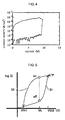
- Fig. 5 shows an example of voltage-current characteristics of an organic bistable material, which shows the above switching behavior.
- As shown in Fig. 5, the organic bistable material has two current-voltage characteristics of a high resistance property 51 (off state) and a low resistance property 52 (on state), and has such a nonlinear response property that under a bias Vb, an applied voltage of Vth2 or more causes transition from the off state to the on state and an applied voltage of Vth1 or less causes transition from the on state to the off state to change the resistance value. Thus, by applying a voltage of at least Vth2 or at most Vth1 to the organic bistable material, a so-called switching operation can be carried out. The voltages of Vth1 and Vth2 may be applied as pulse voltages.
- Various organic complexes are known as the organic bistable materials showing the nonlinear response. For example, R. S. Potember, et al. have experimentally produced a switching element that uses a Cu-TCNQ (copper-tetracyanoquinodimethan) complex to have two stable resistance values corresponding to voltage (see Non-Patent Document 1).
- Further, Kumai, et al. have used a single crystal of a K-TCNQ (potassium-tetracyanoquinodimethan) complex to observe a switching behavior due to nonlinear response (see Non-Patent Document 2).
- Furthermore, Adachi, et al. have formed a Cu-TCNQ complex thin film by using a vacuum deposition method to clarify its switching characteristics, and have studied with respect to the applicability to organic EL matrixes (see Non-Patent Document 3).
Non-Patent Document 1: R. S. Potember, et al., Appl. Phys. Lett., 34 (1979), 405
Non-Patent Document 2: Kumai, et al., Kotai Butsuri, 35 (2000), 35
Non-Patent Document 3: Adachi, et al., Oyo Butsuri Gakkai Yokoshu, Spring 2002, Third issue, 1236 - However, switching elements using the above mentioned organic charge transfer complexes have the following disadvantages.
- The switching elements are poor in repeatability of the switching behaviors, and all the elements cannot show the switching characteristics even if they are produced under the same production conditions. Thus, the switching elements are disadvantageous in the lower ratio of switching or transition (transition probability).
- Though causes of the unevenness have not been clarified, the following reasons are possible. In the transition from the off state to the on state shown in Fig. 5, a charge has to be injected from a metal electrode to an organic film. The interface between the organic material film and the metal electrode has microscopic roughness, and it is considered that, in the transition from the off to on state, the charge is injected to the organic material film due to the electrostatic focusing in the rough portion. While the roughness of the interface depends on flatness of the electrode and the organic material film, it is difficult to control the microscopic roughness, so that the transition voltage is inevitably made uneven.
- In view of the problems of the above prior arts, an object of the present invention is to provide a switching element comprising an organic bistable material between electrodes, which has stabilized switching characteristics with a high ratio of switching (a high transition probability).
- Thus, the switching element of the present invention comprises an organic bistable material layer between at least two electrodes, the organic bistable material layer containing an organic bistable compound having two stable resistance values to an applied voltage, and is characterized in that the element comprises thin films of a first electrode layer, a metal microparticle-containing layer, the organic bistable material layer, and a second electrode layer formed in this order, and the metal microparticle-containing layer contains a metal microparticle and the organic bistable compound.
- In the switching element of the invention, the metal microparticle-containing layer, which is formed by adding the metal microparticle into the organic bistable material, is disposed between the first electrode layer and the organic bistable material layer, whereby energy barrier to charge injection from the first electrode 20 to the metal microparticle dispersion layer can be lowered by the metal microparticle. Thus, the energetic interference with the charge injection can be removed, so that the transition probability can be increased by the removal and also by the electrostatic focusing effect of the metal microparticle.
- In the invention, it is preferred that a charge is injected from the first electrode layer through the metal microparticle-containing layer to the organic bistable material layer, and the metal microparticle-containing layer has an energy barrier to the first electrode layer lower than that of the organic bistable material layer.
- In this embodiment, the energy barrier of the metal microparticle-containing layer to the first electrode layer is lower than that of the organic bistable material layer to the first electrode layer. Thus, the charge can be easily injected from the first electrode layer to the organic bistable material layer, to increase the transition probability of the element.
- In the invention, it is preferred that the metal microparticle-containing layer is formed by codepositing a metal and the organic bistable compound. In this embodiment, nano-order metal microparticles can be easily formed by deposition, and the metal microparticle and the organic bistable compound can be codeposited into a uniform layer, whereby the transition probability of the element can be further increased.
- In the invention, it is also preferred that the metal microparticle-containing layer is formed by applying a solution containing the metal microparticle and the organic bistable compound. Also in this embodiment, the metal microparticle and the organic bistable compound can be formed to a uniform layer, whereby the transition probability of the element can be further increased.
- In the invention, it is preferred that the organic bistable compound is a compound represented by the following structural formula (I).

- In the formula (I), R1 to R4 each represent a hydrogen atom, an alkyl group having 1 to 6 carbon atoms which may have a substituent, or an aryl group which may have a substituent, and R1 to R4 may be the same or different ones. R5 and R6 each represent a hydrogen atom, an alkyl group having 1 to 6 carbon atoms which may have a substituent, an aryl group which may have a substituent, or a heterocycle which may have a substituent, and R5 and R6 may be the same or different ones. X represents oxygen or sulfur.
- In this embodiment, an electron can be easily injected to the above quinomethane-based compound from the first electrode because the compound has a low LUMO level, and the compound shows an electron transport property and excellent bistability to be suitable for the invention because the compound has a quinone group of an electron-accepting functional group.
- Further, in the invention, in a case where the organic bistable compound is represented by the structural formula (I), the first electrode layer preferably comprises aluminum and the second electrode preferably comprises gold. In this embodiment, because aluminum is an electrode material having a lower absolute work function value to easily release an electron, and gold is an electrode material having a higher absolute work function value to hardly release an electron, the combination thereof can be preferably used in the electrodes in the invention to achieve the charge injection with ease.
- Furthermore, in the invention, in a case where the organic bistable compound is represented by the structural formula (I), the metal microparticle preferably comprises aluminum. In this embodiment, aluminum is preferably used because it shows an electron-releasing property in the compound of the structural formula (I) and acts to reduce the energy level relatively.
- In the present invention, in the switching element comprising an organic bistable material between electrodes, the transition probability can be increased to stabilize the switching characteristics.
-
- Fig. 1
- is a schematic structural view showing an embodiment of the switching element of the present invention.
- Fig. 2
- is a view showing an energy level of the switching element of Example 1.
- Fig. 3
- is a view showing an energy level of the switching element of Comparative Example 1.
- Fig. 4
- is a view showing a current-voltage characteristic of the switching element of Example 1.
- Fig. 5
- is a view schematically showing a volt-ampere characteristic of conventional switching elements.
- The present invention will be described in detail with reference to drawings below. Fig. 1 is a schematic structural view showing an embodiment of the switching element of the invention.
- As shown in Fig. 1, the switching element has such a structure that thin films of a
first electrode layer 20a, a metal microparticle-containinglayer 40, an organicbistable material layer 30, and asecond electrode layer 20b are stacked in this order on asubstrate 10. - The
substrate 10 is not particularly limited, and a known glass substrate, etc. is preferably used as the substrate. - Materials of the
first electrode layer 20a and thesecond electrode layer 20b are not particularly limited and may be appropriately selected from metal materials such as aluminum, gold, silver, nickel, and iron, inorganic materials such as ITO and carbon, organic materials such as organic conjugated materials and liquid crystals, semiconductor materials such as silicon, etc. - For example, in a case where the quinomethane-based compound of the above structural formula (I) is used as the organic bistable compound for the organic
bistable material layer 30 to be hereinafter described, it is preferred that thefirst electrode layer 20a adjacent to the metal microparticle-containinglayer 40 is an aluminum electrode and thesecond electrode layer 20b adjacent to the organicbistable material layer 30 is a gold electrode. Aluminum has a lower absolute value of work function (WF) among electrode materials and thus can release an electron easily, and gold has a higher absolute value of work function among electrode materials and thus cannot release an electron easily, so that they are preferably used to cause charge injection with ease. - In the first and second electrode layers, the absolute value of work function means a minimum energy required for removing an electron from a surface of a material, which is a characteristic value specific for each electrode material. The work function can be measured from a photoelectric emission spectrum in the air. Electrode materials with low absolute values of work function other than aluminum include lithium, magnesium, calcium, silver, etc., and materials with high absolute values of work function other than gold include chromium, platinum, ITO, etc.
- A method for forming the
first electrode layer 20a and thesecond electrode layer 20b is not particularly limited, and a known thin film forming method such as a vacuum deposition method, etc. may be preferably used. In the case of forming the thin film by vacuum deposition, the substrate temperature is preferably 0 to 150°C in the deposition step though it is appropriately selected depending on the electrode material. The thickness of each electrode layer is preferably 50 to 200 nm. - The organic bistable compound for the organic
bistable material layer 30 has a functional group for transporting a charge, and preferably is a compound at least containing a compound containing an electron-releasing functional group and an electron-accepting functional group in a molecule. - The electron-releasing functional groups include -SCH3, -OCH3, -NH2, -NHCH3, -N(CH3)2, etc., and the electron-accepting functional groups include -CN, NO2, -CHO, -COCH3, -COOC2H5, -COOH, -Br, -Cl, -I, -OH, -F, =O, etc., though not restrictive.
- Examples of the above described compound containing the electron-releasing functional group and the electron-accepting functional group in a molecule include organic bistable compounds such as aminoimidazole compounds, dicyano compounds, pyridone compounds, styryl compounds, stilbene compounds, quinomethane-based compounds, and butadiene compounds, while the compound is not limited thereto particularly.
- Among the above ones, the organic bistable compound is preferably a quinomethane compound represented by the following structural formula (I).

- The quinomethane-based compound (I) can be synthesized according to e.g. the following reaction formula.

- Specific examples of the quinomethane-based compounds include the compounds represented by the following structural formulae (I-1) to (I-18).


The organicbistable material layer 30 may be formed by a vacuum deposition method, a spin coating method, an electrolytic polymerization method, a chemical vapor deposition method (a CVD method), a monomolecular film built-up method (a LB method), a dip method, a bar coating method, an ink jet method, a screen printing method, etc., and the forming method is not particularly restricted. - In the case of forming the organic
bistable material layer 30 by vacuum deposition, the substrate temperature in the depositing step is preferably 0 to 100°C though it may be appropriately selected depending on the organic bistable material. The thickness of the layer is preferably 20 to 150 nm. - In the case of forming the organic
bistable material layer 30 by a coating method such as a spin coating method, a solvent for the coating liquid may be a halogen solvent such as dichloromethane, dichloroethane, and chloroform, an ether solvent such as tetrahydrofuran (THF) and ethylene glycol dimethyl ether, an aromatic solvent such as toluene and xylene, an alcohol solvent such as ethyl alcohol, an ester solvent such as ethyl acetate and butyl acetate, a ketone solvent such as acetone and MEK, acetonitrile, etc. 0.001 to 30% by mass of the organic bistable material is dissolved in the solvent, and a binder resin is added thereto if necessary, to prepare the coating liquid. Examples of the binder resins include polycarbonates, polyesters, polyvinyl alcohols, polystyrenes, etc. The condition of the spin coating may be controlled depending on the desired thickness, and the rotation speed is preferably within the range of 200 to 3,600 rpm. - Next the metal microparticle-containing
layer 40 is described. The invention is characterized in that the metal microparticle-containinglayer 40 containing the metal microparticle and the organic bistable compound is disposed between thefirst electrode layer 20a and the organicbistable material layer 30. - The metal microparticle is not particularly limited and may comprise various metal materials such as aluminum, gold, silver, copper, platinum, calcium, lithium, and rhodium. In the case of using the compound of the structural formula (I) as the organic bistable compound, the metal microparticle preferably comprise aluminum from the viewpoint of matching of the energy levels.
- The nano-order metal microparticle is easily available commercially from Tanaka Kikinzoku Kogyo K.K., etc. Further, the metal microparticle can be formed by a vacuum deposition method as described hereinafter.
- The metal microparticle-containing
layer 40 is preferably formed by codepositing the metal microparticle and the organic bistable compound using a vacuum deposition method, etc. In this case, the metal is evaporated, so that metal microparticles of 5 to 20 nm in size can be obtained. By the codeposition process, a uniform hybrid thin film of the metal microparticle and the organic bistable compound can be obtained. - The codeposition process may be carried out by a known deposition apparatus in the same manner as the organic
bistable material layer 30, and the substrate temperature in the process may be selected depending on the organic material and is preferably 0 to 150°C. Further, the vacuum degree is preferably 10-5 torr or less. In the codeposition process, the volume ratio between the metal microparticle and the organic bistable material is preferably within the range of 10:1 to 1:20. Further, the thickness is preferably 3 to 200 nm. - The metal microparticle-containing
layer 40 may be formed by a coating method such as spin coating under conditions equal to those of forming the organicbistable material layer 30. Particularly in the case of using a metal such as platinum and rhodium for the metal microparticle, the coating solvent is preferably an alcohol solvent such as ethyl alcohol, methyl alcohol, and propyl alcohol, a glycol solvent such as ethylene glycol, THF, ethylene glycol dimethyl ether, or pure water, the material being easily dispersed in these solvents. - 0.001 to 30% by mass of the organic bistable material is dissolved in the coating solvent, and 0.001 to 30% by mass of the metal microparticle is dispersed therein. A binder resin is added thereto if necessary to obtain a coating liquid. The binder resin may be a polycarbonate, a polyester, a polyvinyl alcohol, a polystyrene, etc. The spin coating conditions may be appropriately selected depending on the desired thickness, and the rotation number is preferably within the range of 200 to 3,600 rpm. Further, the thickness is preferably 3 to 200 nm.
- In the switching element of the invention produced in the above manner, it is preferred that a charge is injected from the first electrode layer through the metal microparticle-containing layer to the organic bistable material layer, and the energy barrier of the metal microparticle-containing layer to the first electrode layer is lower than that of the organic bistable material layer to the first electrode layer.
- Specifically, in a case where the charge is transported by electrons, it is preferred that the absolute value of work function |WF1| of the
first electrode layer 20a, the absolute value of lowest unoccupied molecular orbital level |LUMOOR| of the organicbistable material layer 30, and the absolute value of lowest unoccupied molecular orbital level |LUMOME| of the metal microparticle-containinglayer 40 satisfy the following relational expressions (A) and (B).

wherein |LUMOOR'| represents the absolute value of lowest unoccupied molecular orbital level of the organic bistable material layer in a case where the first electrode layer and the organic bistable material layer are directly stacked. - On the other hand, in a case where the charge is transported by holes, it is preferred that the absolute value of work function |WF1| of the
first electrode layer 20a, the absolute value of highest occupied molecular orbital level |HOMOOR| of the organicbistable material layer 30, and the absolute value of highest occupied molecular orbital level |HOMOME| of the metal microparticle-containinglayer 40 satisfy the following relational expressions (A') and (B').

wherein |HOMOOR'| represents the absolute value of highest occupied molecular orbital level of the organic bistable material layer in a case where the first electrode layer and the organic bistable material layer are directly stacked. - The absolute value of work function |WF1| of the
first electrode layer 20a can be measured from a photoelectric emission spectrum in the air. - The values of |LUMOOR|, |LUMOME|, |LUMOOR'|, |HOMOOR|, |HOMOME|, and |HOMOOR'| can be measured by calculating electron affinities from ionization potentials obtained by photoelectric emission spectra in the air and band gaps obtained by optical absorption spectra, and by correcting the electron affinities for vacuum level shifts of the layers obtained by the Kelvin method, etc.
- In the above switching element, the mechanism of the high transition probability is partly unclear, and is presumed as follows.
- In general, with respect to energy levels of metal microparticles, the ionization potentials and the electron affinities of single atoms are known (e.g. Kagaku Binran Kisohen II, edited by The Chemical Society of Japan, Maruzen, 1994).
- Further, in clusters comprising aggregated atoms, the energy levels gradually approaches to the bulk work functions (WF) as the number of the aggregated atoms is increased. Thus, when D (nm) represents a cluster diameter of a metal, the following equations are approximately satisfied (Atarashii Kurasuta no kagaku (New Cluster Science), edited by Satoru Sugano, Kodansha Ltd., 2002).


- By adding the metal microparticle to the organic bistable material, the energy barrier to the charge injection from the
first electrode 20a to the metalmicroparticle dispersion layer 40 is lowered due to the effects of the metal microparticle. It is presumed that the energetic interference with the charge injection is thus removed, and the transition probability can be increased by the removal and also by the electrostatic focusing effect of the metal microparticle. - Thus, it is considered that the metal microparticle is dispersed to utilize the electric properties in addition to the uneven transition voltage-preventing effect of the electrostatic focusing due to the roughness of the microparticle, whereby the transition probability can be increased by the shift of Fermi levels.
- The switching element of the present invention will be described in further detail below with reference to Examples.
- A switching element having a structure shown in Fig. 1 was produced in the following manner. Thus, a glass substrate was used as a
substrate 10, and thin films of afirst electrode layer 20a, a metal microparticle-containinglayer 40, an organicbistable material layer 30, and asecond electrode layer 20b were formed in this order by a vacuum deposition method, to obtain the switching element of Example 1. - As deposition sources, aluminum was used for the
first electrode layer 20a, gold was used for thesecond electrode layer 20b, and the quinomethane compound represented by the following structural formula (I-1) was used for the organicbistable material layer 30. The metal microparticle-containinglayer 40 was formed by codepositing aluminum and a quinomethane compound represented by the structural formula (II) at a volume ratio of 3:1. - The deposition steps were carried out by a resistance heating method using a diffusion pump exhaust apparatus at a vacuum degree of 3 × 10⁻⁶ torr.

- A switching element of Example 2 was produced in the same manner as Example 1 except that the metal microparticle-containing
layer 40 had a thickness of 15 nm. - A switching element of Example 3 was produced in the same manner as Example 1 except that the compound of the following structural formula (1-5) was used as a quinomethane-based compound, and the thicknesses of the
first electrode layer 20a, the metal microparticle-containinglayer 40, the organicbistable material layer 30, and thesecond electrode layer 20b were 100 nm, 20 nm, 60 nm, and 100 nm, respectively.
- A switching element of Example 4 was produced in the same manner as Example 1 except that the compound of the following structural formula (I-6) was used as a quinomethane-based compound, and the thicknesses of the
first electrode layer 20a, the metal microparticle-containinglayer 40, the organicbistable material layer 30, and thesecond electrode layer 20b were 100 nm, 30 nm, 80 nm, and 100 nm, respectively.
- A switching element of Comparative Example 1 was produced in the same manner as Example 1 except that the metal microparticle-containing
layer 40 was not formed, and thefirst electrode layer 20a, the organicbistable material layer 30, and thesecond electrode layer 20b were formed in this order. - A switching element of Comparative Example 2 was produced in the same manner as Example 3 except that the metal microparticle-containing
layer 40 was not formed, and thefirst electrode layer 20a, the organicbistable material layer 30, and thesecond electrode layer 20b were formed in this order. - The energy levels (unit: eV) of the switching elements of Example 1 and Comparative Example 1 were measured. The results are shown in Table 1 and Figs. 2 and 3. WF (the absolute value of work function) and the lowest unoccupied molecular orbital level (the LUMO level) of each layer were measured by an atmospheric photoelectric emission spectrum method using AC-1 manufactured by Riken Keiki Co., Ltd. and Kelvin method using FAC-1 manufactured by Riken Keiki Co., Ltd.
[Table 1] First electrode layer 20aMetal microparticle-containing layer 40Organic bistable material layer 30Example 1 |WF1| |LUMOME| |HOMOME| |LUMOOR| |HOMOOR| 4.20 eV 4.63 eV 6.58 eV 4.35 eV 6.30 eV Comparative Example 1 |WF1| |LUMOME| |HOMOME| |LUMOOR'| |HOMOOR'| 4.20 eV - - 3.28 eV 5.23 eV - In the metal microparticle-containing
layer 40 of Example 1 of Table 1 and Fig. 2, the LUMO level, which was an energy level of the electron conduction band of the organic material, was lowered by dispersion of the aluminum microparticle. It is presumed that e.g. a donor impurity (a electron-releasing impurity) is introduced near the electron affinity level, and the Fermi level is shifted to the electron affinity and corresponds to that of the adjacent layer, whereby the energy level is lowered. Thus, it is considered that the aluminum microparticle acted as the donor impurity (the electron-releasing impurity) for the organicbistable material layer 30 to lower the LUMO level. - Thus, in the switching element of Example 1, when the quinomethane compound (II) was an electron-transporting compound, the
first electrode 20a acted as an earth, and thesecond electrode 20b acted as a plus bias, electrons were injected from thefirst electrode 20a through the metal microparticle-containinglayer 40 to the organicbistable material layer 30, to obtain the bistable characteristics. - Further, the energy barrier of the metal microparticle-containing
layer 40 to the organicbistable material layer 30 of Fig. 2 was lower than that of theelectrode 21 a to the organicbistable material layer 30 of Fig. 3. It is considered that the result was obtained because the metal microparticle-containinglayer 40 contained the same organic bistable material as the organicbistable material layer 30. - On the other hand, as shown in Fig. 3, in Comparative Example 1 the energy level (the LUMO level) of the organic
bistable material layer 30 was higher than that of thefirst electrode 20a, whereby electrons were not easily injected to the organicbistable material layer 30. - The current-voltage characteristics of 50 switching elements according to each of Examples 1 to 4 and Comparative Examples 1 and 2 were measured at the room temperature while using the
first electrode 20a as an earth and using thesecond electrode 20b as a plus bias, to obtain the transition probability and Vth2 of the threshold voltage shown in Fig. 5. The results are shown in Table 1. Further, a current-voltage characteristic of the switching element according to Example 1 was shown in Fig. 4.Table 2 Transition probability (%) Vth2 (average value) Example 1 98 7.8 Example 2 96 9.6 Example 3 100 8.6 Example 4 98 8.4 Comparative Example 1 64 7.8 Comparative Example 2 54 8.4 - It is clear from the results shown in Table 2 that the transition probabilities of Examples were remarkably increased as compared with Comparative Examples. Further, as shown in Fig. 4, the element of Example 1 showed the low resistance state/high resistance state ratio of about 1,000 or more, which is an excellent bistable characteristic.
- The switching element of the present invention can be suitably used for driving display panels using organic EL elements, liquid crystals, etc., or for high-density memories, etc.
Claims (7)
- A switching element comprising an organic bistable material layer between at least two electrodes, the organic bistable material layer containing an organic bistable compound having two stable resistance values to an applied voltage, characterized in that the switching element comprises thin films of a first electrode layer, a metal microparticle-containing layer, the organic bistable material layer, and a second electrode layer formed in this order, and the metal microparticle-containing layer contains a metal microparticle and the organic bistable compound.
- The switching element according to claim 1, wherein the switching element is adapted to injecting a charge from the first electrode layer through the metal microparticle-containing layer to the organic bistable material layer, and the metal microparticle-containing layer has an energy barrier to the first electrode layer lower than that of the organic bistable material layer.
- The switching element according to claim 1 or 2, wherein the metal microparticle-containing layer is formed by codepositing a metal and the organic bistable compound.
- The switching element according to claim 1 or 2, wherein the metal microparticle-containing layer is formed by applying a solution containing the metal microparticle and the organic bistable compound.
- The switching element according to any one of claims 1 to 4, wherein the organic bistable compound is represented by the following structural formula (I):

- The switching element according to claim 5, wherein the first electrode layer comprises aluminum and the second electrode layer comprises gold.
- The switching element according to claim 5 or 6, wherein the metal microparticle comprises aluminum.
Applications Claiming Priority (2)
| Application Number | Priority Date | Filing Date | Title |
|---|---|---|---|
| JP2003295146 | 2003-08-19 | ||
| PCT/JP2004/011604 WO2005018009A1 (en) | 2003-08-19 | 2004-08-12 | Switching device |
Publications (2)
| Publication Number | Publication Date |
|---|---|
| EP1657760A1 true EP1657760A1 (en) | 2006-05-17 |
| EP1657760A4 EP1657760A4 (en) | 2007-10-17 |
Family
ID=34191082
Family Applications (1)
| Application Number | Title | Priority Date | Filing Date |
|---|---|---|---|
| EP04771579A Withdrawn EP1657760A4 (en) | 2003-08-19 | 2004-08-12 | SWITCHING DEVICE |
Country Status (4)
| Country | Link |
|---|---|
| US (1) | US7807991B2 (en) |
| EP (1) | EP1657760A4 (en) |
| JP (1) | JP4729721B2 (en) |
| WO (1) | WO2005018009A1 (en) |
Cited By (4)
| Publication number | Priority date | Publication date | Assignee | Title |
|---|---|---|---|---|
| WO2007035259A1 (en) | 2005-09-15 | 2007-03-29 | Spansion Llc | Semiconductor memory device comprising one or more injecting bilayer electrodes |
| FR2905028A1 (en) * | 2006-08-21 | 2008-02-22 | Commissariat Energie Atomique | ELECTROCHEMICAL MEMORY DEVICE |
| DE102007037069A1 (en) * | 2007-08-06 | 2009-02-19 | Leonhard Kurz Gmbh & Co. Kg | Electronic component i.e. organic FET, for electrical circuit, has auxiliary layer arranged in direct contact with semiconductor layer and including islands that are electrically insulated from each other |
| US8218351B2 (en) | 2008-03-13 | 2012-07-10 | Commissariat A L'energie Atomique | Non-volatile electrochemical memory device |
Families Citing this family (6)
| Publication number | Priority date | Publication date | Assignee | Title |
|---|---|---|---|---|
| US7170779B2 (en) * | 2004-06-17 | 2007-01-30 | Canon Kabushiki Kaisha | Non-volatile memory using organic bistable device |
| JP5002293B2 (en) * | 2007-03-20 | 2012-08-15 | 株式会社東芝 | Program display device and program display method |
| JP2008277827A (en) * | 2007-04-25 | 2008-11-13 | Hynix Semiconductor Inc | Nonvolatile memory device and manufacturing method thereof |
| JP2012088401A (en) * | 2010-10-15 | 2012-05-10 | Seiko Instruments Inc | Bistable liquid crystal device |
| JP6203154B2 (en) * | 2014-09-22 | 2017-09-27 | 東芝メモリ株式会社 | Organic molecular memory |
| CN116794904A (en) * | 2023-04-18 | 2023-09-22 | 安徽大学 | Optical bistable device of ternary photonic crystal structure based on graphene |
Family Cites Families (8)
| Publication number | Priority date | Publication date | Assignee | Title |
|---|---|---|---|---|
| JP3476932B2 (en) * | 1994-12-06 | 2003-12-10 | シャープ株式会社 | Ferroelectric thin film, substrate coated with ferroelectric thin film, and method of manufacturing ferroelectric thin film |
| JP3725335B2 (en) * | 1998-06-25 | 2005-12-07 | 株式会社東芝 | Organic thin film element |
| US6950331B2 (en) * | 2000-10-31 | 2005-09-27 | The Regents Of The University Of California | Organic bistable device and organic memory cells |
| JP2003238561A (en) | 2002-02-13 | 2003-08-27 | Fuji Denki Gazo Device Kk | Quinomethane compounds |
| JP3712062B2 (en) | 2002-02-04 | 2005-11-02 | 富士電機画像デバイス株式会社 | Electrophotographic photoreceptor and electrophotographic apparatus using the same |
| JPWO2004073079A1 (en) * | 2003-02-14 | 2006-06-01 | 富士電機ホールディングス株式会社 | Switching element |
| JP4826254B2 (en) | 2003-02-17 | 2011-11-30 | 富士電機株式会社 | Switching element |
| US6987689B2 (en) * | 2003-08-20 | 2006-01-17 | International Business Machines Corporation | Non-volatile multi-stable memory device and methods of making and using the same |
-
2004
- 2004-08-12 US US10/558,259 patent/US7807991B2/en not_active Expired - Fee Related
- 2004-08-12 EP EP04771579A patent/EP1657760A4/en not_active Withdrawn
- 2004-08-12 WO PCT/JP2004/011604 patent/WO2005018009A1/en not_active Ceased
- 2004-08-12 JP JP2005513177A patent/JP4729721B2/en not_active Expired - Fee Related
Cited By (7)
| Publication number | Priority date | Publication date | Assignee | Title |
|---|---|---|---|---|
| WO2007035259A1 (en) | 2005-09-15 | 2007-03-29 | Spansion Llc | Semiconductor memory device comprising one or more injecting bilayer electrodes |
| US7582893B2 (en) | 2005-09-15 | 2009-09-01 | Spansion Llc | Semiconductor memory device comprising one or more injecting bilayer electrodes |
| FR2905028A1 (en) * | 2006-08-21 | 2008-02-22 | Commissariat Energie Atomique | ELECTROCHEMICAL MEMORY DEVICE |
| EP1892723A1 (en) * | 2006-08-21 | 2008-02-27 | Commissariat à l'Energie Atomique | Electrochemical memory device |
| US7652907B2 (en) | 2006-08-21 | 2010-01-26 | Commissariat A L'energie Atomique | Electrochemical memory device |
| DE102007037069A1 (en) * | 2007-08-06 | 2009-02-19 | Leonhard Kurz Gmbh & Co. Kg | Electronic component i.e. organic FET, for electrical circuit, has auxiliary layer arranged in direct contact with semiconductor layer and including islands that are electrically insulated from each other |
| US8218351B2 (en) | 2008-03-13 | 2012-07-10 | Commissariat A L'energie Atomique | Non-volatile electrochemical memory device |
Also Published As
| Publication number | Publication date |
|---|---|
| JP4729721B2 (en) | 2011-07-20 |
| US20070172697A1 (en) | 2007-07-26 |
| US7807991B2 (en) | 2010-10-05 |
| WO2005018009A1 (en) | 2005-02-24 |
| JPWO2005018009A1 (en) | 2007-10-04 |
| EP1657760A4 (en) | 2007-10-17 |
Similar Documents
| Publication | Publication Date | Title |
|---|---|---|
| US7919195B2 (en) | System for displaying images | |
| US6830830B2 (en) | Semiconducting hole injection materials for organic light emitting devices | |
| KR101640621B1 (en) | Organic electronic component and method for the production thereof | |
| KR20050013209A (en) | Memory device having a semiconducting polymer film | |
| EP1997814B1 (en) | Electronic Device Including a Buffer Layer Comprising A Functionalized Metal Nanoparticle | |
| EP1594176B1 (en) | Switching device | |
| JPH06267658A (en) | Organic el element | |
| US7807991B2 (en) | Switching element | |
| Li et al. | Efficient and Stable OLEDs with Inverted Device Structure Utilizing Solution‐Processed ZnO‐Based Electron Injection Layer | |
| US20040101711A1 (en) | Azulene-based compounds in organic light emitting device elements | |
| JP4254228B2 (en) | Switching element and manufacturing method thereof | |
| US7786470B2 (en) | Switching element | |
| US6847541B2 (en) | Information storage device, and information storage method and information regeneration method employing the information storage device | |
| JP4618131B2 (en) | Switching element | |
| JP2020186281A (en) | Coating film, coating film laminate, coating film laminate manufacturing method, and electronic device | |
| US7645777B2 (en) | Switching device | |
| JPWO2005041318A1 (en) | Switching element | |
| EP1729356A1 (en) | Switching device | |
| JP5923338B2 (en) | Transistor element | |
| Kondo | Current-voltage characteristics of organic semiconductors: Interfacial control between organic layers and electrodes | |
| WO2007069416A1 (en) | Organic semiconductor material, organic semiconductor film, organic semiconductor device and organic thin film transistor | |
| JP2006054241A (en) | Rectifier element | |
| JP2004200570A (en) | Switching element and manufacturing method thereof |
Legal Events
| Date | Code | Title | Description |
|---|---|---|---|
| PUAI | Public reference made under article 153(3) epc to a published international application that has entered the european phase |
Free format text: ORIGINAL CODE: 0009012 |
|
| 17P | Request for examination filed |
Effective date: 20060127 |
|
| AK | Designated contracting states |
Kind code of ref document: A1 Designated state(s): DE FR |
|
| DAX | Request for extension of the european patent (deleted) | ||
| RBV | Designated contracting states (corrected) |
Designated state(s): DE FR |
|
| A4 | Supplementary search report drawn up and despatched |
Effective date: 20070918 |
|
| 17Q | First examination report despatched |
Effective date: 20081230 |
|
| RAP1 | Party data changed (applicant data changed or rights of an application transferred) |
Owner name: FUJI ELECTRIC CO., LTD. |
|
| GRAP | Despatch of communication of intention to grant a patent |
Free format text: ORIGINAL CODE: EPIDOSNIGR1 |
|
| INTG | Intention to grant announced |
Effective date: 20151023 |
|
| RIC1 | Information provided on ipc code assigned before grant |
Ipc: G11C 13/00 20060101ALI20151009BHEP Ipc: H01L 51/30 20060101ALI20151009BHEP Ipc: B82Y 10/00 20110101AFI20151009BHEP |
|
| STAA | Information on the status of an ep patent application or granted ep patent |
Free format text: STATUS: THE APPLICATION IS DEEMED TO BE WITHDRAWN |
|
| 18D | Application deemed to be withdrawn |
Effective date: 20160303 |