EP1653474A1 - Programming method of multilevel memories and corresponding circuit - Google Patents
Programming method of multilevel memories and corresponding circuit Download PDFInfo
- Publication number
- EP1653474A1 EP1653474A1 EP05022651A EP05022651A EP1653474A1 EP 1653474 A1 EP1653474 A1 EP 1653474A1 EP 05022651 A EP05022651 A EP 05022651A EP 05022651 A EP05022651 A EP 05022651A EP 1653474 A1 EP1653474 A1 EP 1653474A1
- Authority
- EP
- European Patent Office
- Prior art keywords
- programming
- verify
- ver
- prog
- operations
- Prior art date
- Legal status (The legal status is an assumption and is not a legal conclusion. Google has not performed a legal analysis and makes no representation as to the accuracy of the status listed.)
- Withdrawn
Links
- 230000015654 memory Effects 0.000 title claims abstract description 56
- 238000000034 method Methods 0.000 title claims abstract description 21
- 239000011159 matrix material Substances 0.000 claims abstract description 7
- 230000015468 UV-damage excision repair Effects 0.000 claims description 4
- 238000009826 distribution Methods 0.000 description 5
- 230000001105 regulatory effect Effects 0.000 description 4
- 238000012795 verification Methods 0.000 description 2
- 101150027978 UMOD gene Proteins 0.000 description 1
- 230000001276 controlling effect Effects 0.000 description 1
- 230000006870 function Effects 0.000 description 1
- 238000004519 manufacturing process Methods 0.000 description 1
- 238000002360 preparation method Methods 0.000 description 1
Images


Classifications
-
- G—PHYSICS
- G11—INFORMATION STORAGE
- G11C—STATIC STORES
- G11C8/00—Arrangements for selecting an address in a digital store
- G11C8/10—Decoders
-
- G—PHYSICS
- G11—INFORMATION STORAGE
- G11C—STATIC STORES
- G11C11/00—Digital stores characterised by the use of particular electric or magnetic storage elements; Storage elements therefor
- G11C11/56—Digital stores characterised by the use of particular electric or magnetic storage elements; Storage elements therefor using storage elements with more than two stable states represented by steps, e.g. of voltage, current, phase, frequency
- G11C11/5621—Digital stores characterised by the use of particular electric or magnetic storage elements; Storage elements therefor using storage elements with more than two stable states represented by steps, e.g. of voltage, current, phase, frequency using charge storage in a floating gate
- G11C11/5628—Programming or writing circuits; Data input circuits
-
- G—PHYSICS
- G11—INFORMATION STORAGE
- G11C—STATIC STORES
- G11C16/00—Erasable programmable read-only memories
- G11C16/02—Erasable programmable read-only memories electrically programmable
- G11C16/06—Auxiliary circuits, e.g. for writing into memory
- G11C16/10—Programming or data input circuits
-
- G—PHYSICS
- G11—INFORMATION STORAGE
- G11C—STATIC STORES
- G11C8/00—Arrangements for selecting an address in a digital store
- G11C8/18—Address timing or clocking circuits; Address control signal generation or management, e.g. for row address strobe [RAS] or column address strobe [CAS] signals
-
- G—PHYSICS
- G11—INFORMATION STORAGE
- G11C—STATIC STORES
- G11C2211/00—Indexing scheme relating to digital stores characterized by the use of particular electric or magnetic storage elements; Storage elements therefor
- G11C2211/56—Indexing scheme relating to G11C11/56 and sub-groups for features not covered by these groups
- G11C2211/562—Multilevel memory programming aspects
- G11C2211/5621—Multilevel programming verification
Definitions
- the present invention relates to a method for programming multilevel memories and to a corresponding circuit.
- the invention relates to a method for programming multilevel memories of the flash EEPROM type wherein the memory comprises a matrix of cells organised in rows and columns and grouped in memory words.
- the invention particularly, but not exclusively, relates to a circuit of the above type for NROM flash memories with two-bit cells and the following description is made with reference to this field of application by way of illustration only.
- a fundamental operation in multilevel memories is the programming one.
- a first known solution to meet this need is represented by a multilevel programming method which uses a sequence of programming and verification pulses.
- the method can be divided in two steps: a first real multilevel step, used for constructing the distributions "10" and "01” and a subsequent quicker step for constructing the distribution "00". It should be noted that the programming of the cells "00" does not necessarily require to continuously verify the evolution of the threshold of the cells under programming.
- a programming step comprises a series of box-like voltage pulses applied to the gate terminal of the cells to be programmed, alternated by verify operations.
- the width of the programmed distribution is function of the voltage difference between two successive pulses and of the precision with which the cell terminals are regulated; in general, a precise regulation of the voltage implies a slowness of the regulation itself.
- the verify and programming operations require two different voltage levels applied to the gate terminal.
- Figure 1 shows the drain Vdrain and gate Vgate voltages of a memory cell during a multilevel programming.
- the programming Vgi and verify Vv voltage values are obtained by a same charge pump circuit.
- Figure 2 by way of example, globally and schematically shows a programming circuit 100 of a multilevel memory cell.
- first supply block 1 comprising, for example, a charge pump 1a, intended to supply voltage values for programming and verify operations and a second supply block 2, comprising a charge pump 2a intended to supply voltage values for read operations of memory cells.
- the charge pump 1a has a first output line Umod, whereas the second charge pump 2a, a second output line Uread.
- a voltage Vxs which is regulated by the two charge pumps 1a, 2a is brought, through a switch 4, to the input of a row decoder 3, in turn connected to word lines WLs of the multilevel memory.
- the switch 4 selects the operation which is to be performed on a corresponding multilevel memory cell, ie. programming, verifying and reading.
- the switch 4 comprises a voltage elevator or booster 5 which has an input connected to a logic gate 6 in turn receiving at an input an enable signal SECT_EN and an operative mode signal MOD.
- the signal SECT_EN enables a sector whereon an operation has to be performed, whereas the operative mode signal MOD identifies the operation which is to be performed, i.e. programming, verifying or reading.
- this multilevel programming method shows various drawbacks.
- the management, by a single supply block 1 and, in particular by the single charge pump 1a, of the switches of the voltage Vxs on the word line WLs, from a programming voltage level to the verify one and vice versa requires a considerable time.
- the circuit 100 by means of the charge pump 1a, increases the voltage Vxs for a successive programming pulse of a cell, only after the end of a verify operation; in consequence, before emitting a new pulse quite a long time Tvpi will have to be awaited. Moreover, the time required also increases when the absolute value of the difference between the verify voltage and the voltage of the pulse produced by the charge pump 1a voltage increases, as shown in figure 1 wherein Tvpi > Tvpi+1 and Tvpi > Tvp i+1 . In consequence, the management of the switches tends to become slower and slower.
- the technical problem underlying the present invention is that of providing a multilevel programming method, having such functional characteristics as to allow to reduce the programming times of multilevel cells, overcoming the limits and the drawbacks still affecting the known methods.
- the solution idea underlying the present invention is that of providing a simultaneous generation of programming and verify voltage values for biasing the word lines of a multilevel memory device.
- figure 4 shows a programming circuit of multilevel memories according to a first preferred embodiment, globally indicated with 200.
- the circuit 200 is associated with a matrix of multilevel memory cells, not shown in the drawings since conventional. Only a plurality of connections WLS under the rows or word lines of the memory cells of this matrix are schematically indicated, each one being associated with a corresponding decode circuit.
- first supply block 11 comprising a first charge pump 12 and a second supply block 21, comprising a second charge pump 22.
- the first charge pump 12 is intended to supply voltage values for read operations of memory cells and it has a first output line U.
- the second charge pump 22 is intended to supply voltage values for programming and verify operations of memory cells.
- the second charge pump 22 has a second output line U PROG and a third output line U VER , respectively intended to transmit a programming voltage value V PROG and a verify voltage value V VER for the programming or verify steps of memory cells.
- V PROG is regulated at various voltage levels and it is used for biasing the word lines WLs during the programming pulses
- V VER is set at a fixed value and it is used for biasing the word lines WLs during the verify operations.
- the two regulation voltages V PROG and V VER are suitably managed through an inner regulation of the circuit 200 and they are connected to the row decoding through a dedicated switch 14.
- a voltage Vxs having a value equal to V PROG while programming and V VER while verifying and being regulated by the two charge pumps 12 and 22 is supplied, through the switch 14, at the input of a row decoder 13, in turn connected to word lines WLs of the multilevel memory.
- the switch 14 selects the operation which is to be performed on a corresponding multilevel memory cell, i.e. programming or verify.
- the switch 14 intended for the management of the voltage VXS, manages a new high voltage signal.
- a verify signal VER as shown in figure 4, is added, according to the present invention, to the control signals of the prior art switch 4.
- the switch 14 comprises a voltage elevator or booster 15 which has an input connected to a logic gate 16, in turn receiving at inputs an enable signal SECT_EN, an operative mode signal MOD and a verify signal VER_N.
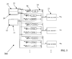
- Figure 5 shows a programming circuit of multilevel memories according to a second embodiment and globally indicated with 300, wherein components and signals shared by figure 4 will be indicated with the same reference labels.
- the first supply block 11 comprising the first charge pump 12; such charge pump 12 has an output line U, intended to supply voltage values for read operations of memory cells, as already described with reference to the circuit 200 shown in figure 4.
- the second supply block 21 comprises two separate charge pumps and, precisely, a third charge pump 23 and a fourth charge pump 24.
- the third charge pump 23 has an output line U2 PROG , for biasing of word lines WLs for programming operations of memory cells, whereas the fourth charge pump 24 has an output line U2 VER , for biasing word lines WLs for verify operations of memory cells.
- the management of the voltage sources U PROG and U VER is different from the one presented in the prior art, due to the presence of a new verify signal VER at the input of the gate 16.
- Figure 3 shows the patterns of the programming voltage V PROG , verify voltage V VER as well as the drain voltage Vdrain and gate voltages Vgi, Vv of the cell to be programmed or verified, respectively, on the basis of the multilevel programming method, according to the present invention.
- verify signal to an operative value.
- verify pulse a verify operation is required.
- Vgate starts to decrease to reach a successive programming voltage value.
- Vgate reaches a programming voltage value Vg2.
- the control signal VER is activated and deactivated by an algorithm.
- the control signal MOD in the proposed solution is activated at hardware level further to a program control signal (however it could be also managed by an algorithm).
- the voltage signals V PROG and V VER are simultaneously raised up, respectively for the programming and the verification of memory cells with transistor; such cells, in consequence, are biased with Vgate values equal to Vgi and Vv .
- the simultaneous availability of the two above sources allows to prepare the voltage level Vgi+1 of the successive cell programming voltage, once the current pulse has just ended, while the value of the verify voltage VV is constant and always available.
- the switching wait time Tvp between a verify voltage value and a programming one becomes short being the programming voltage value to be applied to the gate yet ready, similarly the switching time Tpv between a programming voltage value and a verify one is reduced, since the verify voltage is always available.
- the two circuit solutions moreover, occupy the same area on integrated circuit with respect to the prior art solutions.
- the multilevel programming described in the present invention allows an optimisation of the management of the gate voltages for programming and verify operations, being more efficient in terms of time with respect to what is described in the prior art, minimising the times of the transients between programming and verify operations.
- the manufacturing on integrated circuit does not require an area being greater with respect to the prior art to be used.
Landscapes
- Engineering & Computer Science (AREA)
- Microelectronics & Electronic Packaging (AREA)
- Computer Hardware Design (AREA)
- Read Only Memory (AREA)
Abstract
Description
- The present invention relates to a method for programming multilevel memories and to a corresponding circuit.
- More specifically, the invention relates to a method for programming multilevel memories of the flash EEPROM type wherein the memory comprises a matrix of cells organised in rows and columns and grouped in memory words.
- The invention particularly, but not exclusively, relates to a circuit of the above type for NROM flash memories with two-bit cells and the following description is made with reference to this field of application by way of illustration only.
- As it is well known in semiconductor-integrated memory electronic devices the need of a greater and greater "density" has led to the development of so-called multilevel memories, i.e. memories wherein each single flash cell memorises a number of bits greater than one.
- A fundamental operation in multilevel memories is the programming one. In fact, in the case of multilevel memories, with respect to the programming of single-level memories, it is necessary to control, in a very accurate way, the threshold voltage values of the multilevel cell.
- A first known solution to meet this need is represented by a multilevel programming method which uses a sequence of programming and verification pulses.
- Making reference, by way of non limiting example, to a memory with two bits per cell, if the distribution of the cells "00" is considered as a single-level distribution, the method can be divided in two steps: a first real multilevel step, used for constructing the distributions "10" and "01" and a subsequent quicker step for constructing the distribution "00". It should be noted that the programming of the cells "00" does not necessarily require to continuously verify the evolution of the threshold of the cells under programming.
- In a classical multilevel programming method, a programming step comprises a series of box-like voltage pulses applied to the gate terminal of the cells to be programmed, alternated by verify operations. The width of the programmed distribution is function of the voltage difference between two successive pulses and of the precision with which the cell terminals are regulated; in general, a precise regulation of the voltage implies a slowness of the regulation itself. The verify and programming operations require two different voltage levels applied to the gate terminal.
- Figure 1 shows the drain Vdrain and gate Vgate voltages of a memory cell during a multilevel programming. The gate voltage Vgate switches between different values, for controlling the programming and verify operations of a cell, employing a time Tpvi for switching from a programming voltage value (
Vgi 1=1..N) to a verify voltage value (Vv) and a time Tvpi for performing the contrary switch. - The programming Vgi and verify Vv voltage values are obtained by a same charge pump circuit.
- Figure 2, by way of example, globally and schematically shows a
programming circuit 100 of a multilevel memory cell. - In the circuit there are a
first supply block 1, comprising, for example, a charge pump 1a, intended to supply voltage values for programming and verify operations and asecond supply block 2, comprising acharge pump 2a intended to supply voltage values for read operations of memory cells. The charge pump 1a has a first output line Umod, whereas thesecond charge pump 2a, a second output line Uread. - A voltage Vxs which is regulated by the two
charge pumps 1a, 2a is brought, through aswitch 4, to the input of arow decoder 3, in turn connected to word lines WLs of the multilevel memory. Theswitch 4 selects the operation which is to be performed on a corresponding multilevel memory cell, ie. programming, verifying and reading. - The
switch 4 comprises a voltage elevator orbooster 5 which has an input connected to alogic gate 6 in turn receiving at an input an enable signal SECT_EN and an operative mode signal MOD. The signal SECT_EN enables a sector whereon an operation has to be performed, whereas the operative mode signal MOD identifies the operation which is to be performed, i.e. programming, verifying or reading. - Although advantageous under several aspects, this multilevel programming method shows various drawbacks.
- In particular, the management, by a
single supply block 1 and, in particular by the single charge pump 1a, of the switches of the voltage Vxs on the word line WLs, from a programming voltage level to the verify one and vice versa requires a considerable time. - The
circuit 100, by means of the charge pump 1a, increases the voltage Vxs for a successive programming pulse of a cell, only after the end of a verify operation; in consequence, before emitting a new pulse quite a long time Tvpi will have to be awaited. Moreover, the time required also increases when the absolute value of the difference between the verify voltage and the voltage of the pulse produced by the charge pump 1a voltage increases, as shown in figure 1 wherein Tvpi > Tvpi+1 and Tvpi > Tvpi+1. In consequence, the management of the switches tends to become slower and slower. - The technical problem underlying the present invention is that of providing a multilevel programming method, having such functional characteristics as to allow to reduce the programming times of multilevel cells, overcoming the limits and the drawbacks still affecting the known methods.
- The solution idea underlying the present invention is that of providing a simultaneous generation of programming and verify voltage values for biasing the word lines of a multilevel memory device.
- On the basis of such solution idea the technical problem is solved by a method as previously indicated and defined by the characterising part of
claim 1. - The problem is also solved by a circuit as previously indicated and defined by the characterising part of
claim 4. - The characteristics and advantages of the method and of the circuit according to the invention will be apparent from the following description of an embodiment thereof given by way of indicative and non limiting example with reference to the annexed drawings.
- In such drawings:
- figure 1 schematically shows the patterns in time of the gate and drain voltages of a multilevel memory cell, during a multilevel programming performed according to the prior art;
- figure 2 schematically shows a multilevel programming circuit realised according to the prior art;
- figure 3 schematically shows the patterns in time of the drain and gate voltages of a multilevel memory cell, during a multilevel programming performed with the method according to the present invention;
- figure 4 schematically shows a first preferred embodiment of a multilevel programming circuit, according to the present invention;
- figure 5 schematically shows a second preferred embodiment of a multilevel programming circuit, according to the invention.
- With reference to such figures, figure 4 shows a programming circuit of multilevel memories according to a first preferred embodiment, globally indicated with 200.
- The
circuit 200 is associated with a matrix of multilevel memory cells, not shown in the drawings since conventional. Only a plurality of connections WLS under the rows or word lines of the memory cells of this matrix are schematically indicated, each one being associated with a corresponding decode circuit. - In the
circuit 200 there is afirst supply block 11, comprising afirst charge pump 12 and asecond supply block 21, comprising asecond charge pump 22. - The
first charge pump 12 is intended to supply voltage values for read operations of memory cells and it has a first output line U. Thesecond charge pump 22 is intended to supply voltage values for programming and verify operations of memory cells. - Advantageously, according to the invention, the
second charge pump 22 has a second output line UPROG and a third output line UVER, respectively intended to transmit a programming voltage value VPROG and a verify voltage value VVER for the programming or verify steps of memory cells. - Advantageously, according to the invention, VPROG is regulated at various voltage levels and it is used for biasing the word lines WLs during the programming pulses, whereas VVER is set at a fixed value and it is used for biasing the word lines WLs during the verify operations.
- The two regulation voltages VPROG and VVER are suitably managed through an inner regulation of the
circuit 200 and they are connected to the row decoding through adedicated switch 14. - A voltage Vxs, having a value equal to VPROG while programming and VVER while verifying and being regulated by the two
charge pumps switch 14, at the input of arow decoder 13, in turn connected to word lines WLs of the multilevel memory. - The
switch 14 selects the operation which is to be performed on a corresponding multilevel memory cell, i.e. programming or verify. - With respect to the prior art the
switch 14, intended for the management of the voltage VXS, manages a new high voltage signal. In fact a verify signal VER, as shown in figure 4, is added, according to the present invention, to the control signals of theprior art switch 4. - The
switch 14 comprises a voltage elevator orbooster 15 which has an input connected to alogic gate 16, in turn receiving at inputs an enable signal SECT_EN, an operative mode signal MOD and a verify signal VER_N. - Figure 5 shows a programming circuit of multilevel memories according to a second embodiment and globally indicated with 300, wherein components and signals shared by figure 4 will be indicated with the same reference labels.
- In the
circuit 300 there is thefirst supply block 11, comprising thefirst charge pump 12;such charge pump 12 has an output line U, intended to supply voltage values for read operations of memory cells, as already described with reference to thecircuit 200 shown in figure 4. Advantageously, according to the invention, thesecond supply block 21, comprises two separate charge pumps and, precisely, athird charge pump 23 and afourth charge pump 24. - Advantageously, according to the present invention, the
third charge pump 23 has an output line U2PROG, for biasing of word lines WLs for programming operations of memory cells, whereas thefourth charge pump 24 has an output line U2VER, for biasing word lines WLs for verify operations of memory cells. - The operation is now described of the
circuits - In both the preferred embodiments, the management of the voltage sources UPROG and UVER is different from the one presented in the prior art, due to the presence of a new verify signal VER at the input of the
gate 16. - The use of this signal together with the operative mode signal MOD implies a method for programming the multilevel memories of the
circuits - During read operations of a memory cell, the operative mode MOD and verify VER signals will be both at a low logic value; in other words:

- During verify operations of a memory cell, the operative mode signal MOD will be at a low logic value, whereas the verify signal VER will be at a high logic value; in other words, there will be:

- During programming operations of a memory cell, the operative mode signal MOD will be at a high logic value, whereas the verify signal VER will be at a low logic value; in other words, there will be:

- Figure 3 shows the patterns of the programming voltage VPROG, verify voltage VVER as well as the drain voltage Vdrain and gate voltages Vgi, Vv of the cell to be programmed or verified, respectively, on the basis of the multilevel programming method, according to the present invention.
- More in detail,
- At time t=t0: all the signals are at a low logic value.
- At time t=t1: simultaneous initialisation of the programming and verify signals. The voltage signals VPROG and VVER switch to a high logic value simultaneously, causing the start of a variation of the gate voltage Vgate.
- At time t=t2: programming pulse; a programming operation is required. The circuit thus brings the operative mode signal MOD to a high logic value (MOD=1) and it keeps the verify signal VER at a low logic value (VER=0). The gate voltage of the memory cell to be programmed is set at a control value VPROG = Vgate = Vg1.
- At time t=t3: verify signal to an operative value. The verify signal VVER reaches its operative value VVER =VV, waiting to be used for verify operations.
- At time t=t4 : programming pulse end.
- At time t=t5 : simultaneous preparation of programming voltages for successive operations. The value of the gate voltage Vgate starts to increase for reaching the verify voltage value VV. The programming voltage VPROG starts to increase for preparing the successive programming voltage level Vg2.
- At time t=t6: gate terminal with verify value. The gate reaches a voltage value Vgate=VV, ready to be used for verify operations. Advantageously, according to the invention, the switching time interval Tvp between a programming voltage value and a verify one, such that t5<=Tpv<=t6 is lower than the solutions of the prior art, being the verify voltage value VV already available at the time t=t3.
- At time t=t7: verify pulse; a verify operation is required. The circuit thus brings the verify signal VER to a high logic value (VER=1) and it brings the operative mode signal MOD to a low logic value (MOD=0). Simultaneously a new programming pulse value Vg2 becomes available, for a successive programming operation.
- At time t=t9 : Vgate starts to decrease to reach a successive programming voltage value.
- At time t=t10 : Vgate reaches a programming voltage value Vg2. Advantageously according to the invention, the switching time interval Tvp between a verify voltage value and a programming one, such that t8<=Tvp<=t10, is lower than the solutions of the prior art, being the verify voltage value Vg2 already available at time t=t7.
- The control signal VER is activated and deactivated by an algorithm. The control signal MOD in the proposed solution is activated at hardware level further to a program control signal (however it could be also managed by an algorithm).
- Advantageously, according to the invention, the voltage signals VPROG and VVER are simultaneously raised up, respectively for the programming and the verification of memory cells with transistor; such cells, in consequence, are biased with Vgate values equal to Vgi and Vv .
- Advantageously according to the invention, the simultaneous availability of the two above sources allows to prepare the voltage
level Vgi+ 1 of the successive cell programming voltage, once the current pulse has just ended, while the value of the verify voltage VV is constant and always available. - With the proposed method, the switching wait time Tvp between a verify voltage value and a programming one, becomes short being the programming voltage value to be applied to the gate yet ready, similarly the switching time Tpv between a programming voltage value and a verify one is reduced, since the verify voltage is always available.
- The two circuit solutions, according to the two preferred embodiments, moreover, occupy the same area on integrated circuit with respect to the prior art solutions.
- In conclusion, the multilevel programming described in the present invention allows an optimisation of the management of the gate voltages for programming and verify operations, being more efficient in terms of time with respect to what is described in the prior art, minimising the times of the transients between programming and verify operations. Moreover, the manufacturing on integrated circuit does not require an area being greater with respect to the prior art to be used.
Claims (6)
- Method for programming a multilevel memory of the flash EEPROM type comprising a matrix of cells grouped in memory words and associated with a row decoder circuit (13) supplied by a first (11) and by a second (21) supply blocks associated with corresponding charge pumps, characterised in that it provides the simultaneous generation of a first programming voltage value (VPROG) and a second verify voltage value (VVER), suitable to bias word lines (WLs) of said memory matrix, respectively during programming and verify operations of the memory itself.
- Method according to claim 1, wherein said first programming voltage value (VPROG) and said second verify voltage value (VVER) are applied simultaneously, respectively on two output lines (UPROG, UVER) of a second charge pump (22) of said second supply block (21).
- Method according to claim 1, wherein said first programming voltage value (VPROG) and second verify voltage value (VVER) are applied simultaneously, respectively on an output line (U2PROG) of a third charge pump (23) and on an output line (U2VER) of a fourth charge pump (24), said third (23) and fourth (24) charge pumps being comprised in said second supply block (21).
- Programming circuit of multilevel memories comprising:- a first supply block (11) suitable to generate voltage values for read operations of memory cells;- a second supply block (21) suitable to generate voltage values for programming and verify operations of memory cells;- a row decoder (13), suitable to select the word lines of the memory cells to be selected;- a switch (14), suitable to select the programming or verify operation which is to be performed on memory cells;and characterised in that said second supply block (21) has a first output line (UPROG) and a second output line (UVER), the first one being suitable to bias word lines for programming operations, the second one being suitable to bias word lines for verify operations.
- Circuit according to claim 4, wherein said first (11) and second (21) supply blocks respectively comprise a first (12) and a second (22) charge pumps.
- Programming circuit of multilevel memories comprising:- a first supply block (11) suitable to generate voltage values for read operations of memory cells;- a second supply block (21) suitable to generate voltage values for programming and verify operations of memory cells;- a row decoder (13), suitable to select the word lines of memory cells to be programmed;- a switch (14), suitable to select the programming or verify operation which is to be performed on memory cells;and characterised in that said second supply block (21) comprises a third (23) and a fourth (24) charge pumps, the third charge pump (23) having an output line (U2PROG) suitable to bias word lines for programming operations, the fourth charge pump (24) having an output line (U2VER) suitable to bias word lines for verify operations.
Applications Claiming Priority (1)
| Application Number | Priority Date | Filing Date | Title |
|---|---|---|---|
| IT002071A ITMI20042071A1 (en) | 2004-10-29 | 2004-10-29 | METHOD OF PROGRAMMING OF MULTILEVEL MEMORIES AND RELATIVE CIRCUIT |
Publications (1)
| Publication Number | Publication Date |
|---|---|
| EP1653474A1 true EP1653474A1 (en) | 2006-05-03 |
Family
ID=35709233
Family Applications (1)
| Application Number | Title | Priority Date | Filing Date |
|---|---|---|---|
| EP05022651A Withdrawn EP1653474A1 (en) | 2004-10-29 | 2005-10-18 | Programming method of multilevel memories and corresponding circuit |
Country Status (3)
| Country | Link |
|---|---|
| US (1) | US7317637B2 (en) |
| EP (1) | EP1653474A1 (en) |
| IT (1) | ITMI20042071A1 (en) |
Families Citing this family (11)
| Publication number | Priority date | Publication date | Assignee | Title |
|---|---|---|---|---|
| US7499319B2 (en) * | 2006-03-03 | 2009-03-03 | Sandisk Corporation | Read operation for non-volatile storage with compensation for coupling |
| US7436733B2 (en) * | 2006-03-03 | 2008-10-14 | Sandisk Corporation | System for performing read operation on non-volatile storage with compensation for coupling |
| US7440331B2 (en) * | 2006-06-01 | 2008-10-21 | Sandisk Corporation | Verify operation for non-volatile storage using different voltages |
| US7457163B2 (en) * | 2006-06-01 | 2008-11-25 | Sandisk Corporation | System for verifying non-volatile storage using different voltages |
| US7310272B1 (en) * | 2006-06-02 | 2007-12-18 | Sandisk Corporation | System for performing data pattern sensitivity compensation using different voltage |
| US7450421B2 (en) * | 2006-06-02 | 2008-11-11 | Sandisk Corporation | Data pattern sensitivity compensation using different voltage |
| US7495962B2 (en) * | 2006-12-29 | 2009-02-24 | Sandisk Corporation | Alternating read mode |
| US7606070B2 (en) * | 2006-12-29 | 2009-10-20 | Sandisk Corporation | Systems for margined neighbor reading for non-volatile memory read operations including coupling compensation |
| US7440324B2 (en) * | 2006-12-29 | 2008-10-21 | Sandisk Corporation | Apparatus with alternating read mode |
| US7518923B2 (en) | 2006-12-29 | 2009-04-14 | Sandisk Corporation | Margined neighbor reading for non-volatile memory read operations including coupling compensation |
| FR3012654A1 (en) | 2013-10-25 | 2015-05-01 | St Microelectronics Rousset | METHOD OF WRITING AND READING A DELEGALLY PROGRAMMABLE AND DELEGALLY MULTI-LEVEL DEAD MEMORY AND CORRESPONDING MEMORY DEVICE |
Citations (2)
| Publication number | Priority date | Publication date | Assignee | Title |
|---|---|---|---|---|
| US20010040825A1 (en) * | 2000-04-26 | 2001-11-15 | Naoaki Sugimura | Analog voltage supply circuit for a non-volatile memory |
| US20030206469A1 (en) * | 1998-06-23 | 2003-11-06 | Wong Sau C. | High data rate write process for non-volatile flash memories |
Family Cites Families (3)
| Publication number | Priority date | Publication date | Assignee | Title |
|---|---|---|---|---|
| US5661685A (en) * | 1995-09-25 | 1997-08-26 | Xilinx, Inc. | Programmable logic device with configurable power supply |
| US6134148A (en) * | 1997-09-30 | 2000-10-17 | Hitachi, Ltd. | Semiconductor integrated circuit and data processing system |
| US6977850B2 (en) * | 2001-12-27 | 2005-12-20 | Kabushiki Kaisha Toshiba | Semiconductor device having switch circuit to supply voltage |
-
2004
- 2004-10-29 IT IT002071A patent/ITMI20042071A1/en unknown
-
2005
- 2005-10-18 EP EP05022651A patent/EP1653474A1/en not_active Withdrawn
- 2005-10-27 US US11/261,903 patent/US7317637B2/en not_active Expired - Lifetime
Patent Citations (2)
| Publication number | Priority date | Publication date | Assignee | Title |
|---|---|---|---|---|
| US20030206469A1 (en) * | 1998-06-23 | 2003-11-06 | Wong Sau C. | High data rate write process for non-volatile flash memories |
| US20010040825A1 (en) * | 2000-04-26 | 2001-11-15 | Naoaki Sugimura | Analog voltage supply circuit for a non-volatile memory |
Also Published As
| Publication number | Publication date |
|---|---|
| US20060120161A1 (en) | 2006-06-08 |
| ITMI20042071A1 (en) | 2005-01-29 |
| US7317637B2 (en) | 2008-01-08 |
Similar Documents
| Publication | Publication Date | Title |
|---|---|---|
| KR0159455B1 (en) | A semiconductor integrated circuit device | |
| KR100555243B1 (en) | Semiconductor memory device and control method thereof | |
| US7064986B2 (en) | Non-volatile semiconductor memory device using differential start programming voltage and programming method thereof | |
| US6621745B1 (en) | Row decoder circuit for use in programming a memory device | |
| US8593882B2 (en) | Semiconductor memory device and method of erasing the same | |
| US6747893B2 (en) | Storing data in non-volatile memory devices | |
| KR100586680B1 (en) | Nonvolatile semiconductor memory device | |
| US6240019B1 (en) | Non-volatile semiconductor memory device having a function for controlling the range of distribution of memory cell threshold voltages | |
| KR20120061574A (en) | Pump circuit and semiconductor memory device having the same | |
| US20090147595A1 (en) | Semiconductor integrated circuit device | |
| US8553465B2 (en) | Semiconductor memory device and method of programming the same | |
| US20100302853A1 (en) | Nonvolatile memory device and method of programming the same | |
| US7952935B2 (en) | Nonvolatile memory device and program or verification method using the same | |
| US7317637B2 (en) | Programming method of multilevel memories and corresponding circuit | |
| US6762956B2 (en) | High-speed data programmable nonvolatile semiconductor memory device | |
| US20060268619A1 (en) | Nonvolatile memory using a two-step cell verification process | |
| KR100706245B1 (en) | NOR flash memory device and its program method using bit scan method | |
| US7154785B2 (en) | Charge pump circuitry having adjustable current outputs | |
| KR20090000407A (en) | Voltage providing device and flash memory device having same | |
| CN101303893A (en) | Nonvolatile semiconductor memory device and programming method thereof | |
| KR100572302B1 (en) | A flash memory device and method for programming the same | |
| KR20090123511A (en) | Nonvolatile Memory Device and Operation Method | |
| KR100553715B1 (en) | Multi Level High Voltage Regulator | |
| KR100635195B1 (en) | Flash memory device | |
| KR20060075161A (en) | Program word line voltage generation circuit of a nonvolatile semiconductor memory device whose start and end voltages are controlled |
Legal Events
| Date | Code | Title | Description |
|---|---|---|---|
| PUAI | Public reference made under article 153(3) epc to a published international application that has entered the european phase |
Free format text: ORIGINAL CODE: 0009012 |
|
| AK | Designated contracting states |
Kind code of ref document: A1 Designated state(s): AT BE BG CH CY CZ DE DK EE ES FI FR GB GR HU IE IS IT LI LT LU LV MC NL PL PT RO SE SI SK TR |
|
| AX | Request for extension of the european patent |
Extension state: AL BA HR MK YU |
|
| 17P | Request for examination filed |
Effective date: 20061026 |
|
| 17Q | First examination report despatched |
Effective date: 20061124 |
|
| AKX | Designation fees paid |
Designated state(s): DE FR GB IT |
|
| STAA | Information on the status of an ep patent application or granted ep patent |
Free format text: STATUS: THE APPLICATION IS DEEMED TO BE WITHDRAWN |
|
| 18D | Application deemed to be withdrawn |
Effective date: 20080520 |