EP1653237A1 - System and method for measuring the specific absorption rate - Google Patents
System and method for measuring the specific absorption rate Download PDFInfo
- Publication number
- EP1653237A1 EP1653237A1 EP20050256757 EP05256757A EP1653237A1 EP 1653237 A1 EP1653237 A1 EP 1653237A1 EP 20050256757 EP20050256757 EP 20050256757 EP 05256757 A EP05256757 A EP 05256757A EP 1653237 A1 EP1653237 A1 EP 1653237A1
- Authority
- EP
- European Patent Office
- Prior art keywords
- electro
- optical
- light
- absorption rate
- biological tissue
- Prior art date
- Legal status (The legal status is an assumption and is not a legal conclusion. Google has not performed a legal analysis and makes no representation as to the accuracy of the status listed.)
- Ceased
Links
Images


Classifications
-
- G—PHYSICS
- G01—MEASURING; TESTING
- G01R—MEASURING ELECTRIC VARIABLES; MEASURING MAGNETIC VARIABLES
- G01R29/00—Arrangements for measuring or indicating electric quantities not covered by groups G01R19/00 - G01R27/00
- G01R29/08—Measuring electromagnetic field characteristics
-
- G—PHYSICS
- G01—MEASURING; TESTING
- G01R—MEASURING ELECTRIC VARIABLES; MEASURING MAGNETIC VARIABLES
- G01R29/00—Arrangements for measuring or indicating electric quantities not covered by groups G01R19/00 - G01R27/00
- G01R29/08—Measuring electromagnetic field characteristics
- G01R29/0864—Measuring electromagnetic field characteristics characterised by constructional or functional features
- G01R29/0878—Sensors; antennas; probes; detectors
- G01R29/0885—Sensors; antennas; probes; detectors using optical probes, e.g. electro-optical, luminiscent, glow discharge, or optical interferometers
-
- G—PHYSICS
- G01—MEASURING; TESTING
- G01N—INVESTIGATING OR ANALYSING MATERIALS BY DETERMINING THEIR CHEMICAL OR PHYSICAL PROPERTIES
- G01N21/00—Investigating or analysing materials by the use of optical means, i.e. using sub-millimetre waves, infrared, visible or ultraviolet light
- G01N21/17—Systems in which incident light is modified in accordance with the properties of the material investigated
- G01N21/55—Specular reflectivity
Definitions
- the present invention relates to a biological tissue equivalent phantom unit (phantom unit) used by a specific absorption rate measuring system for evaluating absorption of electromagnetic wave energy; a specific absorption rate measuring system using the phantom unit; and a method thereof.
- a SAR value is proportional to an electric field (
- 2 ), and is often used for evaluating the energy absorbed by a human body when a cellular phone is used near the human body, SAR being defined by the following Equation 1. [ Equation 1 ] SAR ⁇
- ⁇ and ⁇ represent conductivity [S/m] and density [kg/m3], respectively, of the biological tissue equivalent phantom.
- an electric-field measuring method when measuring SAR, an electric-field measuring method is used, wherein a short dipole detects an electric field generated in a medium (live body), which electric field is converted into SAR using Equation 1.
- Fig. 1 shows a conventional specific absorption rate measuring system 100 that includes a simulated body (phantom) 101 that simulates an electric constant of a human body with liquid, a container 102 into which the liquid is provided, a probe 103 for detecting an electric field, a probe scanner 104, a signal cable 105, an electric field detection apparatus 106, and a processor apparatus 107 for measurement operations and data analysis.
- the electric field generated in the phantom is measured by arranging a measuring target instrument 108, such as a cellular phone, near the specific absorption rate measuring system 100 as shown in Fig. 1.
- the probe 103 for detecting the electric field is scanned in three dimensions by the probe scanner 104, and SAR is measured.
- Fig. 2 shows another specific absorption rate measuring system 200 that includes a phantom 121 that simulates the electric constant of the human body with a solid-state object, a probe 122 for detecting the electric field, a cable 123 for signal transmissions, an electric-field detection apparatus 124, a processor apparatus 125 for measurement operations and data analysis, and a scanner 126.
- the electric field generated in the phantom is measured by arranging a measuring target instrument 127, such as a cellular phone, near the specific absorption rate measuring system 200 as shown in Fig. 2.
- a measuring target instrument 127 such as a cellular phone
- the cellular phone 127 is moved by the scanner 126, and SAR is measured.
- the probe 103 or 122 for detecting the electric field is required.
- Each of the probes 103 and 122 for detecting the electric field includes a detecting element 110 as shown in detail on the right-hand side of Fig. 1.
- an electric field is detected by short dipole elements 111 and 112.
- the electric field is detected by a Schottky diode 113 inserted in a gap, and a detected result in the form of an electrical signal is provided to the corresponding electric-field detection apparatuses 106 and 124 through high resistance wires 114. That is, the Schottky diode 113 detects a voltage generated by the short dipole elements 111, 112 formed with conductors, the length of which is about 2 to 5 mm.
- an electric-field sensor 300 using an optical waveguide type modulator and a laser beam has been developed as shown in Fig. 3.
- the electric-field sensor 300 includes a laser luminous source 131, an electric-field probe 132, an optical waveguide type modulator 133, a minute dipole 134 that consists of metal, and an optical receiving unit 135.
- the electric-field sensor 300 is configured only by dielectric materials, except for the minute dipole 134, it is capable of measuring the electric field with a precision that is higher than the electric-field detecting methods that use the high resistance wires.
- the short dipole is used according to the electric-field measuring method using the electric-field sensor 300, wherein the optical waveguide type modulator and the laser beam are used, the disturbance remains, although the disturbance becomes smaller than in the case of the electric-field measuring methods using the high resistance wires.
- the probe for detecting the electric field, or a 3-dimensional electric-field sensor is moved in the liquid phantom for measuring SAR, the liquid (a phantom solvent) is agitated, and noise is generated by vibration of the probe or sensor. If a time until the solvent settles into a steady state is waited for in order to avoid the noise, measurement will take a long time.
- the present invention provides a specific absorption rate measuring system, a biological tissue equivalent phantom unit, and a method thereof that substantially obviate one or more of the problems caused by the limitations and disadvantages of the related art.
- the invention provides a specific absorption rate measuring system, a biological tissue equivalent phantom unit, and a method thereof as follows.
- the biological tissue equivalent phantom unit includes a biological tissue equivalent phantom for absorbing an electromagnetic wave, two or more electro-optical crystals that have a dielectric constant approximately equal to the dielectric constant of the biological tissue equivalent phantom, the electro-optical crystals being arranged at two or more measurement points set up in the biological tissue equivalent phantom, and two or more optical fibers provided in the biological tissue equivalent phantom for connecting each of the electro-optical crystals to an external destination.
- a high dielectric constant material is applied to the surface of the optical fibers of the biological tissue equivalent phantom unit.
- the specific absorption rate measuring system includes a luminous source for emitting a light, a polarization regulator for adjusting a polarization state of the light emitted by the luminous source, an optical-path switcher for switching the light output by the polarization regulator to each electro-optical crystal one by one, and a specific absorption rate measuring unit for measuring a specific absorption rate by detecting the light reflected by the electro-optical crystal.
- the specific absorption rate measuring method includes a step of arranging two or more electro-optical crystals that have a dielectric constant approximately equal to that of the biological tissue equivalent phantom to two or more measuring points in the biological tissue equivalent phantom, a step of sequentially providing the light to each of the electro-optical crystals through the optical-path switcher, the light being irradiated by the luminous source, where the polarization state of the light is adjusted, a step of reflecting the light that is provided to the electro-optical crystals, a step of leading the light reflected from the electro-optical crystal to an analyzer, and a step of converting the light that passes the analyzer into an electrical signal by a photodetector, and obtaining the specific absorption rate.
- the step of reflecting the light that is provided to the electro-optical crystals of the specific absorption rate measuring method is a step of reflecting the light by a dielectric reflective film prepared on a surface countering a surface, through which the light is provided, of the electro-optical crystal.
- the step of sequentially providing the light to each of the electro-optical crystals through the optical-path switcher of the specific absorption rate measuring method is a step of sequentially providing the light to each of the electro-optical crystals by selecting an optical fiber by the optical-path switcher, wherein the optical-path switcher is connected to each of the electro-optical crystals.
- a high dielectric constant material is applied to the surface of the optical fiber such that the equivalent dielectric constant of the optical fiber becomes substantially equal to the dielectric constant of the biological tissue equivalent phantom.
- the electric-field detecting element is constituted by nonmetallic materials, it is possible to measure the SAR distribution without the disturbance that is generated in the case of the conventional technology. Further, since the electro-optical crystals having a dielectric constant approximately equal to that of the phantom are used as a sensor head, reflection due to difference of the dielectric constants is reduced, and the SAR distribution can be more accurately measured. Furthermore, since spatial resolution of the measurement is proportional to a diameter of a beam of the light that penetrates the electro-optical crystal, the spatial resolution can be raised, theoretically, to as small as the wavelength of the light (several ⁇ m). Furthermore, since a change in a refractive index of the electro-optical crystal at the measuring point depends on deviation of a dipole that follows the electromagnetic wave, the SAR measurement is available in a wide band range, from the MHz band to the THz band.
- the present invention disturbance of the electric field in the electro-optical crystal by interface reflection is reduced, and the influence of the interface reflection on the electromagnetic field near the electro-optical crystals is reduced by using the electro-optical crystal that has a dielectric constant approximately equal to that of the phantom. Therefore, the specific absorption rate measuring system capable of obtaining an accurate SAR distribution is realized.
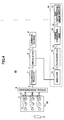
- Fig. 4 is a block diagram of a specific absorption ratio measuring system 40 according to the embodiment of the present invention.
- the specific absorption rate measuring system 40 includes a biological tissue equivalent phantom unit 42 that is constituted by a simulated human body (phantom) 1 consisting of liquid, gel, a solid-state object, etc., for simulating the electric constant of the human body, electro-optical crystals 3 that have a dielectric constant approximately equal to that of the phantom 1, and bare fibers 10.
- the specific absorption rate measuring system 40 further includes an electromagnetic wave generator 2 such as a cellular phone, a linearly polarized luminous source 4 such as DFB-LD, a polarization maintenance fiber (PMF) 5, a circulator 6, a polarization regulator 7 that includes a 1/4 wave plate and a 1/2 wave plate, single mode fibers (SMF) 8, an optical-path switcher 9 that is formed by MEMS technology and PLC technology, and a specific absorption rate measuring unit 44.
- an electromagnetic wave generator 2 such as a cellular phone
- a linearly polarized luminous source 4 such as DFB-LD
- PMF polarization maintenance fiber
- PMF polarization maintenance fiber
- circulator 6 a circulator 6
- a polarization regulator 7 that includes a 1/4 wave plate and a 1/2 wave plate
- SMF single mode fibers
- optical-path switcher 9 that is formed by MEMS technology and PLC technology
- the specific absorption rate measuring unit 44 includes an analyzer 11, a photodetector 12, an electrical signal line 13, a signal processing unit 14, and a SAR distribution image display 15.
- the specific absorption rate measuring system 40 is for measuring an electric field in the phantom 1 using the electro-optical crystals 3, the electric field being generated by the electromagnetic wave generator 2 (such as a cellular phone) arranged near the phantom 1, as shown in Fig. 4.
- the electromagnetic wave generator 2 such as a cellular phone
- the linearly polarized light irradiated by the luminous source 4 is provided to the polarization regulator 7 via the circulator 6 and the polarization maintenance fiber (PMF) 5.
- the polarization regulator 7 changes the polarization of the linearly polarized light into a predetermined polarization state, and outputs the light.
- the polarization state is determined by a crystallographic axis of the electro-optical crystal 3 arranged in the phantom 1 and a vibrating direction of the electric field generated by the electromagnetic wave generator 2.
- CdTe which is a lead marcasite type crystal
- crystallographic faces (001), (100), and (010) of CdTe are perpendicularly arranged to the y, x, and the z axes, respectively; or to the y, z, and x axes, respectively; and the polarization regulator 7 is adjusted so that the polarization axis of the linear polarization or an elliptical polarization may become parallel to the x axis or the z axis.
- the light is transmitted via the single mode fiber (SMF) 8 to the optical-path switcher 9, then to the electro-optical crystals 3.
- SMF single mode fiber
- the light is reflected by a dielectric reflective film prepared on a surface of the electro-optical crystal 3, the surface countering a surface through which the light is provided, and the light goes back along the incidence path.
- a phase difference arises between components of the predetermined polarization due to a refractive-index change (Pockels effect) that is proportional to the field strength to the first power that is applied, and the polarization state is changed, i.e., polarization modulation occurs.
- Equation 2 ( 2 ⁇ / ⁇ ) n 0 8 r 41 Ed
- ⁇ , n o , r 41 , E, and d represent the wavelength [m] of the incident light, the refractive index of the electro-optical crystal 3, the Pockels constant [m/V], field strength [v/m], and the length [m] of the electro-optical crystal 3 in a direction of the oscillation of the electric field, respectively.
- the light that is reflected and polarization-modulated reaches the circulator 6 through the optical-path switcher 9 and the polarization regulator 7; then, the light is branched to the analyzer 11 by the circulator 6.
- the modulation component of the branched light is taken out by the analyzer 11, and is converted into an electrical signal by the photodetector 12.
- the amplitude of the electrical signal is proportional to the field strength of the electromagnetic wave that is measured.
- the amplitude of the electrical signal is converted into a SAR value by the signal processing unit 14.
- Such values, with position information attached, constitute a SAR distribution that can be displayed by the SAR distribution image display 15.
- the specific absorption rate (SAR) is defined by Equation 1.
- K is a constant determined by the crystallographic axis of the electro-optical crystal 3 and the vibrating direction of the electric field irradiated by the electromagnetic wave generator 2.
- the electric-field detecting element is constituted from dielectric materials, the disturbance to the electromagnetic field to be measured is removed, the disturbance conventionally being due to the aggregate of the short dipoles, and the disturbance being the problem with the conventional electric-field measuring method.
- the dielectric constants of the phantom 1 are prescribed by ARIB.
- reflection (Fresnel reflection) of the electromagnetic wave can arise at the interface between the phantom 1 and the electro-optical crystal 3 depending on the kind of the electro-optical crystal 3 according to the difference in the dielectric constants, such reflection is very small as compared with the disturbance due to the aggregate of short dipoles.
- Fig. 6 shows the field strength in the electro-optical crystal 3 in consideration of the reflection at the interface when there is no absorption of the electromagnetic wave within the electro-optical crystal 3.
- a model is assumed wherein the electromagnetic wave is perpendicularly provided to the electro-optical crystal 3 that is semi-infinite in size, and as the relative permittivity of the phantom, a value 40.5 at 1450 MHz that is specified by ARIB is used.
- Calculation results show that a true value can be obtained by compensating for the electric field that is measured by about 10% for the reflection in the case of CdTe. Further, it is considered that the influence on the measured electromagnetic field by the reflection is proportional to an area ratio that the electro-optical crystal 3 occupies.
- the minimum spatial resolution of the SAR measurement is 1 mm
- the minimum processing size of the electro-optical crystal 3 is about 100 ⁇ m
- the reflection factor per mm 2 is converted by the area ratio, it becomes about 1% of 1/100, which can practically be disregarded.
- electro-optical crystals that have a dielectric constant value approximately equal to the dielectric constant value of the phantom are used, such electro-optical crystals including LN, LT, and KD*P.
- the electrical properties of LN, LT, and KD*P and the error in the measured electric field due to the reflection are shown in Table 1.
- the diameter of a common bare fiber is 250 ⁇ m including a covering layer, and the reflection factor per mm 2 of the cross section is 1/16 (about 1.8%).
- the covering layer is provided in consideration of a micro bend property at low temperatures.
- a clad fiber having a diameter of 80 ⁇ m without a covering layer can be used.
- the reflection factor per mm 2 can be lowered to 0.2% or less.
- the number of the bare fibers 10 on the optical-path switcher 9 side per mm 2 is N, and the reflection factor per mm 2 becomes less than 0.2xN%. If the reflection factor is tolerated to be up to 10%, the number of the electro-optical crystals 3 that can be arranged in the direction of the y-axis becomes 50. If they are arranged at intervals of 1 mm, the length wherein the electro-optical crystals 3 are arranged in the direction of the y-axis is 50 mm. Since the size of the phantom that simulates the head is about 300 mm, the reflection by the optical-path switcher 9 may become great.
Abstract
a biological tissue equivalent phantom for absorbing an electromagnetic wave; two or more electro-optical crystals (3) that are arranged at two or more measurement points in the phantom, the electro-optical crystals having a dielectric constant that is approximately equal to that of the phantom; and two or more optical fibers (10) laid in the biological tissue equivalent phantom for optically connecting each of the electro-optical crystals to an external destination. The specific absorption rate measuring system for evaluating absorption of the electromagnetic wave energy using the phantom unit includes
a luminous source (4) for irradiating a light; a polarization regulator (7) for adjusting a polarization state of the light that is output by the luminous source; an optical-path switcher (9) for providing the polarization-adjusted light to each of the electro-optical crystals one by one; and a specific absorption rate measuring unit (44) for detecting the light reflected from the electro-optical crystal, and for measuring an absorption rate.
Description
- The present invention relates to a biological tissue equivalent phantom unit (phantom unit) used by a specific absorption rate measuring system for evaluating absorption of electromagnetic wave energy; a specific absorption rate measuring system using the phantom unit; and a method thereof.
- In recent years and continuing, requirements are increasing for quantitatively evaluating a thermal effect caused by an electromagnetic wave emitted by a wireless radio transmitter; and a system that is capable of accurately and swiftly measuring a specific absorption rate (SAR), which is an index of the reaction of the electromagnetic wave on a living body, such as a human, is desired.
- A SAR value is proportional to an electric field (|E|2), and is often used for evaluating the energy absorbed by a human body when a cellular phone is used near the human body, SAR being defined by the following
Equation 1.
- Here, σ and ρ represent conductivity [S/m] and density [kg/m3], respectively, of the biological tissue equivalent phantom.
- Usually, when measuring SAR, an electric-field measuring method is used, wherein a short dipole detects an electric field generated in a medium (live body), which electric field is converted into
SAR using Equation 1. - Fig. 1 shows a conventional specific absorption
rate measuring system 100 that includes
a simulated body (phantom) 101 that simulates an electric constant of a human body with liquid,
acontainer 102 into which the liquid is provided,
aprobe 103 for detecting an electric field,
aprobe scanner 104,
asignal cable 105,
an electricfield detection apparatus 106, and
aprocessor apparatus 107 for measurement operations and data analysis. - Here, the electric field generated in the phantom is measured by arranging a
measuring target instrument 108, such as a cellular phone, near the specific absorptionrate measuring system 100 as shown in Fig. 1. Theprobe 103 for detecting the electric field is scanned in three dimensions by theprobe scanner 104, and SAR is measured. - Fig. 2 shows another specific absorption rate measuring
system 200 that includes
aphantom 121 that simulates the electric constant of the human body with a solid-state object,
aprobe 122 for detecting the electric field,
acable 123 for signal transmissions,
an electric-field detection apparatus 124,
aprocessor apparatus 125 for measurement operations and data analysis, and
ascanner 126. - The electric field generated in the phantom is measured by arranging a
measuring target instrument 127, such as a cellular phone, near the specific absorptionrate measuring system 200 as shown in Fig. 2. However, unlike the conventional example shown by Fig. 1, thecellular phone 127 is moved by thescanner 126, and SAR is measured. - In either of the conventional examples, the
probe probes element 110 as shown in detail on the right-hand side of Fig. 1. There, an electric field is detected byshort dipole elements diode 113 inserted in a gap, and a detected result in the form of an electrical signal is provided to the corresponding electric-field detection apparatuses high resistance wires 114. That is, the Schottkydiode 113 detects a voltage generated by theshort dipole elements - However, since the short dipole antenna and the high resistance wires, both being conductive, are present in the electric field to be measured, the electromagnetic field distribution near the detecting
element 110 is disturbed. This is a problem of the electric-field measuring method. Further, since it is difficult to reduce the length of thedipole elements - Then, in an attempt to reduce the disturbance to the electromagnetic field generated by the
measuring target 108, 127 (e.g. a cellular phone), the disturbance being due to theprobe field sensor 300 using an optical waveguide type modulator and a laser beam has been developed as shown in Fig. 3. - The electric-
field sensor 300 includes a laserluminous source 131, an electric-field probe 132, an opticalwaveguide type modulator 133, aminute dipole 134 that consists of metal, and anoptical receiving unit 135. - Since the electric-
field sensor 300 is configured only by dielectric materials, except for theminute dipole 134, it is capable of measuring the electric field with a precision that is higher than the electric-field detecting methods that use the high resistance wires. - Nevertheless, since the short dipole is used according to the electric-field measuring method using the electric-
field sensor 300, wherein the optical waveguide type modulator and the laser beam are used, the disturbance remains, although the disturbance becomes smaller than in the case of the electric-field measuring methods using the high resistance wires. Further, since the probe for detecting the electric field, or a 3-dimensional electric-field sensor, is moved in the liquid phantom for measuring SAR, the liquid (a phantom solvent) is agitated, and noise is generated by vibration of the probe or sensor. If a time until the solvent settles into a steady state is waited for in order to avoid the noise, measurement will take a long time. If two or more electric-field sensors are arranged in two dimensions or three dimensions in the phantom in order to shorten the measuring time, the aggregate of the sensors (short dipoles) will behave as a conductor, and will generate a great disturbance to the electromagnetic field to be measured. Consequently, a SAR distribution that is different from actual may be measured, which is a problem. - The present invention provides a specific absorption rate measuring system, a biological tissue equivalent phantom unit, and a method thereof that substantially obviate one or more of the problems caused by the limitations and disadvantages of the related art.
- Features of the present invention are set forth in the description that follows, and in part will become apparent from the description and the accompanying drawings, or may be learned by practice of the invention according to the teachings provided in the description. Problem solutions provided by the present invention will be realized and attained by a specific absorption rate measuring system, a biological tissue equivalent phantom unit, and a method thereof particularly pointed out in the specification in such full, clear, concise, and exact terms as to enable a person having ordinary skill in the art to practice the invention.
- To achieve these solutions and in accordance with the purpose of the invention, as embodied and broadly described herein, the invention provides a specific absorption rate measuring system, a biological tissue equivalent phantom unit, and a method thereof as follows.
- provides a biological tissue equivalent phantom unit that is to be used by a specific absorption rate measuring system for evaluating absorption of electromagnetic wave energy. The biological tissue equivalent phantom unit includes
a biological tissue equivalent phantom for absorbing an electromagnetic wave,
two or more electro-optical crystals that have a dielectric constant approximately equal to the dielectric constant of the biological tissue equivalent phantom, the electro-optical crystals being arranged at two or more measurement points set up in the biological tissue equivalent phantom, and
two or more optical fibers provided in the biological tissue equivalent phantom for connecting each of the electro-optical crystals to an external destination. - According to another aspect of the present invention, a high dielectric constant material is applied to the surface of the optical fibers of the biological tissue equivalent phantom unit.
- Another aspect of the present invention provides a specific absorption rate measuring system for evaluating the absorption of the electromagnetic wave energy using the biological tissue equivalent phantom unit. The specific absorption rate measuring system includes
a luminous source for emitting a light,
a polarization regulator for adjusting a polarization state of the light emitted by the luminous source,
an optical-path switcher for switching the light output by the polarization regulator to each electro-optical crystal one by one, and
a specific absorption rate measuring unit for measuring a specific absorption rate by detecting the light reflected by the electro-optical crystal. - Another aspect of the present invention provides a specific absorption rate measuring method of evaluating absorption of the electromagnetic wave energy using the biological tissue equivalent phantom that receives irradiation of the electromagnetic wave. The specific absorption rate measuring method includes
a step of arranging two or more electro-optical crystals that have a dielectric constant approximately equal to that of the biological tissue equivalent phantom to two or more measuring points in the biological tissue equivalent phantom,
a step of sequentially providing the light to each of the electro-optical crystals through the optical-path switcher, the light being irradiated by the luminous source, where the polarization state of the light is adjusted,
a step of reflecting the light that is provided to the electro-optical crystals,
a step of leading the light reflected from the electro-optical crystal to an analyzer, and
a step of converting the light that passes the analyzer into an electrical signal by a photodetector, and obtaining the specific absorption rate. - According to another aspect of the present invention, the step of reflecting the light that is provided to the electro-optical crystals of the specific absorption rate measuring method is a step of reflecting the light by a dielectric reflective film prepared on a surface countering a surface, through which the light is provided, of the electro-optical crystal.
- According to another aspect of the present invention, the step of sequentially providing the light to each of the electro-optical crystals through the optical-path switcher of the specific absorption rate measuring method is a step of sequentially providing the light to each of the electro-optical crystals by selecting an optical fiber by the optical-path switcher, wherein the optical-path switcher is connected to each of the electro-optical crystals.
- According to another aspect of the present invention, as for the specific absorption rate measuring method, a high dielectric constant material is applied to the surface of the optical fiber such that the equivalent dielectric constant of the optical fiber becomes substantially equal to the dielectric constant of the biological tissue equivalent phantom.
- As described above, according to the present invention, since the electric-field detecting element is constituted by nonmetallic materials, it is possible to measure the SAR distribution without the disturbance that is generated in the case of the conventional technology. Further, since the electro-optical crystals having a dielectric constant approximately equal to that of the phantom are used as a sensor head, reflection due to difference of the dielectric constants is reduced, and the SAR distribution can be more accurately measured. Furthermore, since spatial resolution of the measurement is proportional to a diameter of a beam of the light that penetrates the electro-optical crystal, the spatial resolution can be raised, theoretically, to as small as the wavelength of the light (several µm). Furthermore, since a change in a refractive index of the electro-optical crystal at the measuring point depends on deviation of a dipole that follows the electromagnetic wave, the SAR measurement is available in a wide band range, from the MHz band to the THz band.
- According to the present invention, disturbance of the electric field in the electro-optical crystal by interface reflection is reduced, and the influence of the interface reflection on the electromagnetic field near the electro-optical crystals is reduced by using the electro-optical crystal that has a dielectric constant approximately equal to that of the phantom. Therefore, the specific absorption rate measuring system capable of obtaining an accurate SAR distribution is realized.
-
- Fig. 1 is a schematic diagram of a conventional specific absorption
rate measuring system 100; - Fig. 2 a schematic diagram of another conventional specific absorption
rate measuring system 200; - Fig. 3 is a schematic diagram of another conventional specific absorption
rate measuring system 300 using an optical waveguide type modulator, a laser beam, and an electric-field sensor; - Fig. 4 is a block diagram of a specific absorption rate (SAR) measuring system according to an embodiment of the present invention;
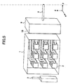
- Fig. 5 is a perspective diagram showing a phantom according to the embodiment of the present invention; and
- Fig. 6 gives a graph showing an error of field strength in an electro-optical crystal, the error being due to difference in dielectric constants.
- In the following, embodiments of the present invention are described with reference to the accompanying drawings, wherein common reference numbers are assigned to items that have the same functions, and the descriptions are not repeated.
- Fig. 4 is a block diagram of a specific absorption
ratio measuring system 40 according to the embodiment of the present invention. The specific absorptionrate measuring system 40 includes a biological tissueequivalent phantom unit 42 that is constituted by a simulated human body (phantom) 1 consisting of liquid, gel, a solid-state object, etc., for simulating the electric constant of the human body, electro-optical crystals 3 that have a dielectric constant approximately equal to that of thephantom 1, andbare fibers 10. - The specific absorption
rate measuring system 40 further includes
anelectromagnetic wave generator 2 such as a cellular phone,
a linearly polarized luminous source 4 such as DFB-LD,
a polarization maintenance fiber (PMF) 5,
acirculator 6,
a polarization regulator 7 that includes a 1/4 wave plate and a 1/2 wave plate,
single mode fibers (SMF) 8,
an optical-path switcher 9 that is formed by MEMS technology and PLC technology, and
a specific absorptionrate measuring unit 44. - The specific absorption
rate measuring unit 44 includes ananalyzer 11, aphotodetector 12, anelectrical signal line 13, asignal processing unit 14, and a SARdistribution image display 15. - The specific absorption
rate measuring system 40 is for measuring an electric field in thephantom 1 using the electro-optical crystals 3, the electric field being generated by the electromagnetic wave generator 2 (such as a cellular phone) arranged near thephantom 1, as shown in Fig. 4. - The linearly polarized light irradiated by the luminous source 4 is provided to the polarization regulator 7 via the
circulator 6 and the polarization maintenance fiber (PMF) 5. The polarization regulator 7 changes the polarization of the linearly polarized light into a predetermined polarization state, and outputs the light. - The polarization state is determined by a crystallographic axis of the electro-
optical crystal 3 arranged in thephantom 1 and a vibrating direction of the electric field generated by theelectromagnetic wave generator 2. For example, when detecting an electric field that vibrates in parallel to the y-axis using CdTe, which is a lead marcasite type crystal, crystallographic faces (001), (100), and (010) of CdTe are perpendicularly arranged to the y, x, and the z axes, respectively; or to the y, z, and x axes, respectively; and the polarization regulator 7 is adjusted so that the polarization axis of the linear polarization or an elliptical polarization may become parallel to the x axis or the z axis. - The light, the polarization of which has been adjusted, is transmitted via the single mode fiber (SMF) 8 to the optical-
path switcher 9, then to the electro-optical crystals 3. - The light is reflected by a dielectric reflective film prepared on a surface of the electro-
optical crystal 3, the surface countering a surface through which the light is provided, and the light goes back along the incidence path. When the light goes back along the incidence path within the electro-optical crystal 3, a phase difference arises between components of the predetermined polarization due to a refractive-index change (Pockels effect) that is proportional to the field strength to the first power that is applied, and the polarization state is changed, i.e., polarization modulation occurs. - When CdTe is arranged, e.g., as described above, a phase difference Γ arises between polarization components that are parallel to the x axis and the z axis, the phase difference Γ being expressed by the following
Equation 2.
- Here, λ, no, r41, E, and d represent the wavelength [m] of the incident light, the refractive index of the electro-
optical crystal 3, the Pockels constant [m/V], field strength [v/m], and the length [m] of the electro-optical crystal 3 in a direction of the oscillation of the electric field, respectively. - The light that is reflected and polarization-modulated reaches the
circulator 6 through the optical-path switcher 9 and the polarization regulator 7; then, the light is branched to theanalyzer 11 by thecirculator 6. The modulation component of the branched light is taken out by theanalyzer 11, and is converted into an electrical signal by thephotodetector 12. The amplitude of the electrical signal is proportional to the field strength of the electromagnetic wave that is measured. The amplitude of the electrical signal is converted into a SAR value by thesignal processing unit 14. Such values, with position information attached, constitute a SAR distribution that can be displayed by the SARdistribution image display 15. - According to the electric-field measuring method, the specific absorption rate (SAR) is defined by
Equation 1. According to the present embodiment, by using the specific absorptionrate measuring system 40, SAR can be defined by the followingEquation 3, based onEquations 
- Here, K is a constant determined by the crystallographic axis of the electro-
optical crystal 3 and the vibrating direction of the electric field irradiated by theelectromagnetic wave generator 2. The constant K can be expressed by the following Equation 4 when CdTe is arranged as described above.
- Further, when detecting the electric field that vibrates parallel to the x (or z) axis by using CdTe, the crystallographic faces (110), (1(1 bar) 0), and (001) of CdTe are arranged perpendicularly to the x(z), y, and z(x) axes, respectively; then the polarization regulator 7 is adjusted so that the polarization axis of the linear polarization or the elliptical polarization may become parallel to the x(z) axis. In this case, a phase difference Γ expressed by the following Equation 5 arises between the polarized components that incline 45° to the x axis and the z axis.

- Here, "1" represents the length [m] of the electro-
optical crystal 3 in the direction of the light passage. Further, when SAR is defined byEquation 3, the constant K can be expressed by the followingEquation 6.
- As described above, according to the specific absorption
rate measuring system 40 of the embodiment, since the electric-field detecting element is constituted from dielectric materials, the disturbance to the electromagnetic field to be measured is removed, the disturbance conventionally being due to the aggregate of the short dipoles, and the disturbance being the problem with the conventional electric-field measuring method. The dielectric constants of thephantom 1 are prescribed by ARIB. Although reflection (Fresnel reflection) of the electromagnetic wave can arise at the interface between thephantom 1 and the electro-optical crystal 3 depending on the kind of the electro-optical crystal 3 according to the difference in the dielectric constants, such reflection is very small as compared with the disturbance due to the aggregate of short dipoles. - Fig. 6 shows the field strength in the electro-
optical crystal 3 in consideration of the reflection at the interface when there is no absorption of the electromagnetic wave within the electro-optical crystal 3. In calculation, a model is assumed wherein the electromagnetic wave is perpendicularly provided to the electro-optical crystal 3 that is semi-infinite in size, and as the relative permittivity of the phantom, a value 40.5 at 1450 MHz that is specified by ARIB is used. Calculation results show that a true value can be obtained by compensating for the electric field that is measured by about 10% for the reflection in the case of CdTe. Further, it is considered that the influence on the measured electromagnetic field by the reflection is proportional to an area ratio that the electro-optical crystal 3 occupies. Given that the minimum spatial resolution of the SAR measurement is 1 mm, and that the minimum processing size of the electro-optical crystal 3 is about 100 µm, if the reflection factor per mm2 is converted by the area ratio, it becomes about 1% of 1/100, which can practically be disregarded. It is also possible to measure SAR without compensation if electro-optical crystals that have a dielectric constant value approximately equal to the dielectric constant value of the phantom are used, such electro-optical crystals including LN, LT, and KD*P. The electrical properties of LN, LT, and KD*P and the error in the measured electric field due to the reflection are shown in Table 1.[Table 1] Electrical properties and error in measured electric field due to interface reflection of electro-optical crystals Electro-optical crystals Pockels constant (x10-12 m/V) Relative permittivity Error in measured electric field LiNbO3 (LN) 19 28 0.8% LiTaO3 (LT) 22 43 <0.01% KD2PO4 (KD*P) 24.1 48 <0.2% - For the same reason, about 28% of reflection occurs at the
bare fiber 10 that connects the optical-path switcher 9 and the electro-optical crystal 3, which reflection may cause a disturbance to the electromagnetic field to be measured. The diameter of a common bare fiber is 250 µm including a covering layer, and the reflection factor per mm2 of the cross section is 1/16 (about 1.8%). The covering layer is provided in consideration of a micro bend property at low temperatures. However, since thebare fiber 10 of the specific absorptionrate measuring system 40 according to the embodiment is covered by thephantom 1, a clad fiber having a diameter of 80 µm without a covering layer can be used. By using the clad fiber, the reflection factor per mm2 can be lowered to 0.2% or less. - With reference to Fig. 5, if N electro-
optical crystals 3 are arranged in the direction of the y-axis, the number of thebare fibers 10 on the optical-path switcher 9 side per mm2 is N, and the reflection factor per mm2 becomes less than 0.2xN%. If the reflection factor is tolerated to be up to 10%, the number of the electro-optical crystals 3 that can be arranged in the direction of the y-axis becomes 50. If they are arranged at intervals of 1 mm, the length wherein the electro-optical crystals 3 are arranged in the direction of the y-axis is 50 mm. Since the size of the phantom that simulates the head is about 300 mm, the reflection by the optical-path switcher 9 may become great. - On the other hand, it is possible to prevent the reflection of the electromagnetic wave from occurring by applying a material having a great dielectric constant to the surface of the
bare fibers 10, making the equivalent dielectric constant equal to the phantom. Since the direction of the main axis and sintering temperature can adjust the specific inductive capacity to a range between 40 and 120, TiO2 and BaTiO3 that have a sintering temperature lower than a softening temperature (about 1500 °C) of glass are suitable as the material to be applied. - Further, the present invention is not limited to these embodiments, but variations and modifications may be made without departing from the scope of the present invention.
Claims (7)
- A biological tissue equivalent phantom unit to be used by a specific absorption rate measuring system for evaluating absorption of electromagnetic wave energy, characterized by:a biological tissue equivalent phantom for absorbing the electromagnetic wave;two or more electro-optical crystals that are arranged at two or more measurement points in the biological tissue equivalent phantom, the electro-optical crystals having a dielectric constant approximately equal to the dielectric constant of the biological tissue equivalent phantom; andtwo or more optical fibers laid in the biological tissue equivalent phantom for coupling each of the electro-optical crystals to an external destination.
- The biological tissue equivalent phantom unit as claimed in claim 1, characterized in that
a high dielectric constant material is applied to a surface of the optical fibers. - The specific absorption rate measuring system for evaluating absorption of electromagnetic wave energy using the biological tissue equivalent phantom unit as claimed in claim 1, characterized by:a luminous source for irradiating a light;a polarization regulator for adjusting a polarization state of the light;an optical-path switcher for providing the light output from the polarization regulator to each of the electro-optical crystals of the live body equivalent phantom unit one by one; anda specific absorption rate measuring unit for detecting the light reflected by the electro-optical crystal, and measuring a specific absorption rate.
- A specific absorption rate measuring method of evaluating absorption of electromagnetic wave energy using a biological tissue equivalent phantom that receives irradiation of the electromagnetic wave, characterized by:a step of arranging two or more electro-optical crystals having a dielectric constant that is approximately equal to the dielectric constant of the biological tissue equivalent phantom to two or more measuring points in the biological tissue equivalent phantom;a step of sequentially providing a light to each of the electro-optical crystals through an optical-path switcher, the light being irradiated by a luminous source, and a polarization state of the light being adjusted;a step of reflecting the light that is provided to the electro-optical crystals;a step of leading the light reflected from the electro-optical crystals to an analyzer; anda step of converting the light that passes into the analyzer into an electrical signal by a photodetector, and obtaining a specific absorption rate.
- The specific absorption rate measuring method as claimed in claim 4, characterized in that
the step of reflecting the light that is provided to the electro-optical crystals is
a step of reflecting the light that is provided to the electro-optical crystals by a dielectric reflective film prepared on a surface of the electro-optical crystals, the surface countering a surface through which the light is provided to the electro-optical crystals. - The specific absorption rate measuring method as claimed in claim 5, characterized in that
the light is sequentially provided to each of the electro-optical crystals by selecting one of a plurality of optical fibers by the optical-path switcher, characterized in that the optical-path switcher is connected to each of the electro-optical crystals by a corresponding one of the optical fibers. - The specific absorption rate measuring method as claimed in claim 6, characterized in that
a high dielectric constant material is applied to a surface of the optical fibers.
Applications Claiming Priority (1)
| Application Number | Priority Date | Filing Date | Title |
|---|---|---|---|
| JP2004319387A JP2006132970A (en) | 2004-11-02 | 2004-11-02 | System and method for measuring specific absorption rate |
Publications (1)
| Publication Number | Publication Date |
|---|---|
| EP1653237A1 true EP1653237A1 (en) | 2006-05-03 |
Family
ID=35781584
Family Applications (1)
| Application Number | Title | Priority Date | Filing Date |
|---|---|---|---|
| EP20050256757 Ceased EP1653237A1 (en) | 2004-11-02 | 2005-11-01 | System and method for measuring the specific absorption rate |
Country Status (6)
| Country | Link |
|---|---|
| US (2) | US20060114003A1 (en) |
| EP (1) | EP1653237A1 (en) |
| JP (1) | JP2006132970A (en) |
| KR (1) | KR20060052388A (en) |
| CN (1) | CN100388008C (en) |
| CA (1) | CA2525158C (en) |
Cited By (2)
| Publication number | Priority date | Publication date | Assignee | Title |
|---|---|---|---|---|
| CN101038313B (en) * | 2007-04-05 | 2011-04-06 | 中兴通讯股份有限公司 | Method for measuring RARTUT specific absorption rate in MAT |
| CN104345068A (en) * | 2013-08-08 | 2015-02-11 | 广州医科大学附属肿瘤医院 | Medical electromagnetic wave energy ratio absorption rate measurement device |
Families Citing this family (23)
| Publication number | Priority date | Publication date | Assignee | Title |
|---|---|---|---|---|
| FR2859064B1 (en) * | 2003-08-18 | 2005-12-30 | Satimo Sa | DEVICE FOR CONTROLLING THE SPECIFIC ABSORPTION RATE OF RADIANT OBJECTS MADE IN SERIES AND IN PARTICULAR PORTABLE TELEPHONES |
| JP2006132970A (en) | 2004-11-02 | 2006-05-25 | Ntt Docomo Inc | System and method for measuring specific absorption rate |
| FR2902523B1 (en) * | 2006-06-16 | 2008-09-05 | Inst Nat Polytech Grenoble | ELECTRO-OPTICAL SENSOR FOR VECTOR MEASUREMENT OF AN ELECTROMAGNETIC FIELD |
| CN101578520B (en) * | 2006-10-18 | 2015-09-16 | 哈佛学院院长等 | Based on formed pattern porous medium cross flow and through biometric apparatus, and preparation method thereof and using method |
| JP5669337B2 (en) * | 2006-10-23 | 2015-02-12 | 株式会社Nttドコモ | System and method for measuring specific absorption rate |
| JP5572281B2 (en) * | 2007-02-28 | 2014-08-13 | 株式会社Nttドコモ | Specific absorption rate measuring apparatus and method |
| JP5376619B2 (en) * | 2008-02-06 | 2013-12-25 | 日本電気株式会社 | Electromagnetic field measuring device |
| US9182434B2 (en) * | 2008-06-10 | 2015-11-10 | University Of Maryland - Office Of Technology | Fast SAR assessment and certification system for wireless device certification |
| JP5221752B2 (en) * | 2009-03-03 | 2013-06-26 | 株式会社エヌ・ティ・ティ・ドコモ | Local average absorbed power measurement method, local average absorbed power calculation device, local average absorbed power calculation program |
| US9468492B2 (en) | 2010-06-03 | 2016-10-18 | Covidien Lp | Specific absorption rate measurement and energy-delivery device characterization using image analysis |
| US9377367B2 (en) | 2010-06-03 | 2016-06-28 | Covidien Lp | Specific absorption rate measurement and energy-delivery device characterization using thermal phantom and image analysis |
| US9241762B2 (en) | 2010-06-03 | 2016-01-26 | Covidien Lp | Specific absorption rate measurement and energy-delivery device characterization using image analysis |
| US8188435B2 (en) | 2010-06-03 | 2012-05-29 | Tyco Healthcare Group Lp | Specific absorption rate measurement and energy-delivery device characterization using thermal phantom and image analysis |
| JP5933030B2 (en) * | 2011-12-29 | 2016-06-08 | インテル・コーポレーション | Display backlight modulation |
| US20150105031A1 (en) * | 2012-04-19 | 2015-04-16 | Telefonaktiebolaget L M Ericsson(Publ) | Efficient Whole-Body SAR Estimation |
| JP6936560B2 (en) * | 2015-06-29 | 2021-09-15 | 国立大学法人大阪大学 | Electromagnetic wave measuring device and electromagnetic wave measuring method |
| CN105974208B (en) * | 2016-05-10 | 2019-02-12 | 上海理工大学 | The measuring system of specific absorption rate under Nuclear Magnetic Resonance |
| CN106333657B (en) * | 2016-10-09 | 2017-12-08 | 京东方科技集团股份有限公司 | A kind of photoelectric sensor and its control method, pulse detector |
| JP6764022B2 (en) * | 2017-04-19 | 2020-09-30 | 学校法人 関西大学 | Biometric information estimation device |
| KR102006666B1 (en) * | 2017-08-24 | 2019-08-02 | 한국표준과학연구원 | Method for acquiring specific absorption rate during MRI scans |
| JP7240995B2 (en) * | 2019-09-17 | 2023-03-16 | 株式会社アドバンテスト | Phantom and fluorescence detector |
| KR102379732B1 (en) * | 2021-03-30 | 2022-03-28 | 한국표준과학연구원 | Method of detecting temperature change and sar of hip joint implant due to mri |
| CN113702715A (en) * | 2021-08-30 | 2021-11-26 | 维沃移动通信有限公司 | Detection device and electronic equipment |
Citations (2)
| Publication number | Priority date | Publication date | Assignee | Title |
|---|---|---|---|---|
| WO2001086311A1 (en) * | 2000-05-05 | 2001-11-15 | Integra Antennas Ltd | A head phantom arrangement and method of measuring of affect of electromagnetic waves by means of this head phantom |
| JP2004012468A (en) * | 2003-08-29 | 2004-01-15 | Nippon Telegr & Teleph Corp <Ntt> | Electric field sensor |
Family Cites Families (18)
| Publication number | Priority date | Publication date | Assignee | Title |
|---|---|---|---|---|
| JP2866912B2 (en) * | 1989-12-15 | 1999-03-08 | 日本電信電話株式会社 | Obstacle Detector for Civil Excavation Propulsion Machine |
| JPH0560818A (en) * | 1991-08-31 | 1993-03-12 | Nippon Dempa Kogyo Co Ltd | Optical electric field measuring instrument |
| JP3192467B2 (en) * | 1992-03-18 | 2001-07-30 | イー・アンド・シー・エンジニアリング株式会社 | Radio wave reflector, anechoic chamber |
| JP2737661B2 (en) * | 1994-09-21 | 1998-04-08 | 日本電気株式会社 | SAR measuring method and SAR measuring device |
| JPH08129054A (en) * | 1994-10-28 | 1996-05-21 | Sumitomo Metal Mining Co Ltd | Apparatus for testing integrated circuit |
| US20010000930A1 (en) * | 1996-08-27 | 2001-05-10 | Kim Roland Y. | Crush-resistant polymeric microcellular wire coating |
| JP3094975B2 (en) * | 1997-11-13 | 2000-10-03 | 日本電気株式会社 | SAR measuring device |
| JP2001324525A (en) * | 2000-05-12 | 2001-11-22 | Nippon Telegr & Teleph Corp <Ntt> | Electric field sensor |
| JP3459394B2 (en) * | 2000-05-31 | 2003-10-20 | 日本電信電話株式会社 | Electric field probe |
| JP2002216998A (en) * | 2001-01-23 | 2002-08-02 | Nisshin:Kk | Plasma density information measuring method and its equipment, and probe for plasma density information measurement, plasma processing method and its equipment |
| JP3727051B2 (en) * | 2001-03-02 | 2005-12-14 | Necトーキン株式会社 | Optical electric field sensor |
| EP2199811B1 (en) * | 2001-08-08 | 2013-01-09 | NTT DoCoMo, Inc. | Apparatus for measuring the specific absorption rate (SAR) of a radio transmitter, in particular a mobile phone, by scanning the transmitter along a dry, solid phantom containing an embedded field probe |
| JP4471583B2 (en) * | 2002-04-22 | 2010-06-02 | パナソニック株式会社 | SAR measuring device |
| EP1359428B1 (en) * | 2002-04-22 | 2005-04-06 | Matsushita Electric Industrial Co., Ltd. | Apparatus for measuring specific absorption rate based on near magnetic field for use in radio apparatus |
| JP3695591B2 (en) * | 2002-10-10 | 2005-09-14 | 株式会社ファインラバー研究所 | Mobile phone |
| CN1419129A (en) * | 2002-12-12 | 2003-05-21 | 华中科技大学 | Optical fibre electric field sensor |
| CN100365420C (en) * | 2003-02-26 | 2008-01-30 | 松下电器产业株式会社 | Apparatus for measuring specific absorption rate of radio communication apparatus |
| JP2006132970A (en) | 2004-11-02 | 2006-05-25 | Ntt Docomo Inc | System and method for measuring specific absorption rate |
-
2004
- 2004-11-02 JP JP2004319387A patent/JP2006132970A/en active Pending
-
2005
- 2005-11-01 EP EP20050256757 patent/EP1653237A1/en not_active Ceased
- 2005-11-01 KR KR20050103779A patent/KR20060052388A/en active Search and Examination
- 2005-11-01 CA CA 2525158 patent/CA2525158C/en not_active Expired - Fee Related
- 2005-11-02 US US11/263,946 patent/US20060114003A1/en not_active Abandoned
- 2005-11-02 CN CNB2005101174872A patent/CN100388008C/en not_active Expired - Fee Related
-
2007
- 2007-05-29 US US11/754,683 patent/US7511511B2/en not_active Expired - Fee Related
Patent Citations (2)
| Publication number | Priority date | Publication date | Assignee | Title |
|---|---|---|---|---|
| WO2001086311A1 (en) * | 2000-05-05 | 2001-11-15 | Integra Antennas Ltd | A head phantom arrangement and method of measuring of affect of electromagnetic waves by means of this head phantom |
| JP2004012468A (en) * | 2003-08-29 | 2004-01-15 | Nippon Telegr & Teleph Corp <Ntt> | Electric field sensor |
Non-Patent Citations (4)
| Title |
|---|
| BERWICK M ET AL: "High precision electromagnetic field sensors for monitoring communications devices", SINGAPORE ICCS '94. CONFERENCE PROCEEDINGS. SINGAPORE 14-18 NOV. 1994, NEW YORK, NY, USA,IEEE, US, vol. 3, 14 November 1994 (1994-11-14), pages 944 - 948, XP010150094, ISBN: 0-7803-2046-8 * |
| HOMBACH ET AL: "The dependence of EM energy absorption upon human head modeling at 900Mhz", IEEE TRANSACTIONS ON MICROWAVE THEORY AND TECHNIQUES, IEEE SERVICE CENTER, PISCATAWAY, NJ, US, vol. 44, no. 10, October 1996 (1996-10-01), pages 1865 - 1873, XP002125147, ISSN: 0018-9480 * |
| PATENT ABSTRACTS OF JAPAN vol. 2003, no. 12 5 December 2003 (2003-12-05) * |
| WAKANA S ET AL INSTITUTE OF ELECTRICAL AND ELECTRONICS ENGINEERS: "NOVEL ELECTROMAGNETIC FIELD PROBE USING ELECTRO/MAGNETO-OPTICAL CRYSTALS MOUNTED ON OPTICAL-FIBER FACETS FOR MICROWAVE CIRCUIT DIAGNOSIS", 2000 IEEE MTT-S INTERNATIONAL MICROWAVE SYMPOSIUM DIGEST. IMS 2000. BOSTON, MA, JUNE 11-16, 2000, IEEE MTT-S INTERNATIONAL MICROWAVE SYMPOSIUM, NEW YORK, NY : IEEE, US, vol. VOL. 3 OF 3, 11 June 2000 (2000-06-11), pages 1615 - 1618, XP000967537, ISBN: 0-7803-5688-8 * |
Cited By (2)
| Publication number | Priority date | Publication date | Assignee | Title |
|---|---|---|---|---|
| CN101038313B (en) * | 2007-04-05 | 2011-04-06 | 中兴通讯股份有限公司 | Method for measuring RARTUT specific absorption rate in MAT |
| CN104345068A (en) * | 2013-08-08 | 2015-02-11 | 广州医科大学附属肿瘤医院 | Medical electromagnetic wave energy ratio absorption rate measurement device |
Also Published As
| Publication number | Publication date |
|---|---|
| US20070236229A1 (en) | 2007-10-11 |
| KR20060052388A (en) | 2006-05-19 |
| US20060114003A1 (en) | 2006-06-01 |
| CA2525158C (en) | 2011-04-19 |
| CA2525158A1 (en) | 2006-05-02 |
| CN1769926A (en) | 2006-05-10 |
| CN100388008C (en) | 2008-05-14 |
| JP2006132970A (en) | 2006-05-25 |
| US7511511B2 (en) | 2009-03-31 |
Similar Documents
| Publication | Publication Date | Title |
|---|---|---|
| EP1653237A1 (en) | System and method for measuring the specific absorption rate | |
| EP0664460B1 (en) | Electric field sensor | |
| CN106093599B (en) | Optical probe and electromagnetic field measuring equipment and measuring method thereof | |
| Togo et al. | Near-field mapping system using fiber-based electro-optic probe for specific absorption rate measurement | |
| Chu et al. | Optical voltage sensors based on integrated optical polarization-rotated reflection interferometry | |
| Togo et al. | Sensitivity-stabilized fiber-mounted electrooptic probe for electric field mapping | |
| Lee et al. | An optical-fiber-scale electro-optic probe for minimally invasive high-frequency field sensing | |
| Kobayashi et al. | Optical bias angle control method for electric field sensor using Mach–Zehnder interferometer | |
| Cecelja et al. | Optimised CdTe sensors for measurement of electric and magnetic fields in the near field region | |
| Dakin et al. | A passive all-dielectric field probe for RF measurement using the electro-optic effect | |
| Togo et al. | Universal optical electric-field sensor covering frequencies from 10 to 100 GHz | |
| JP2013101140A (en) | Specific absorption rate measurement system and method | |
| Euphrasie et al. | Electro-optic sensor for specific absorption rate measurements | |
| Cecelja | Experimental dosimetry for high frequencies | |
| WO2014066384A1 (en) | Shg imaging technique for assessing hybrid eo polymer/silicon photonic integrated circuits | |
| Takahashi et al. | High speed system for measuring electromagnetic field distribution | |
| Auchterlonie et al. | Design features and realisation of a new form of microwave power detector using optical fibres | |
| Ikenaga et al. | Simulated characteristics of optical electric field probe | |
| Cecelja et al. | RF dosimetry using optical techniques | |
| Domański et al. | An optical fiber loop sensor for vibration monitoring | |
| Bassen et al. | An RF field strength measurement system using unintegrated optical linear modulator | |
| Gaborit et al. | Packaged optical sensors for the electric field characterization in harsh environments | |
| Kijima et al. | Electro-optical field sensor using single total internal reflection in electro-optical crystals | |
| Holloway et al. | Development of a new atom-based SI traceable electric-field metrology technique | |
| Ku | Experimental EMF Exposure Assessment |
Legal Events
| Date | Code | Title | Description |
|---|---|---|---|
| PUAI | Public reference made under article 153(3) epc to a published international application that has entered the european phase |
Free format text: ORIGINAL CODE: 0009012 |
|
| 17P | Request for examination filed |
Effective date: 20051108 |
|
| AK | Designated contracting states |
Kind code of ref document: A1 Designated state(s): AT BE BG CH CY CZ DE DK EE ES FI FR GB GR HU IE IS IT LI LT LU LV MC NL PL PT RO SE SI SK TR |
|
| AX | Request for extension of the european patent |
Extension state: AL BA HR MK YU |
|
| 17Q | First examination report despatched |
Effective date: 20061106 |
|
| AKX | Designation fees paid |
Designated state(s): CH DE FI FR GB LI SE |
|
| APBK | Appeal reference recorded |
Free format text: ORIGINAL CODE: EPIDOSNREFNE |
|
| APBN | Date of receipt of notice of appeal recorded |
Free format text: ORIGINAL CODE: EPIDOSNNOA2E |
|
| APBR | Date of receipt of statement of grounds of appeal recorded |
Free format text: ORIGINAL CODE: EPIDOSNNOA3E |
|
| APAF | Appeal reference modified |
Free format text: ORIGINAL CODE: EPIDOSCREFNE |
|
| APBT | Appeal procedure closed |
Free format text: ORIGINAL CODE: EPIDOSNNOA9E |
|
| STAA | Information on the status of an ep patent application or granted ep patent |
Free format text: STATUS: THE APPLICATION HAS BEEN REFUSED |
|
| 18R | Application refused |
Effective date: 20161209 |